WO2023047461A1 - 量子ビット、量子演算装置及び量子ビットの製造方法 - Google Patents
量子ビット、量子演算装置及び量子ビットの製造方法 Download PDFInfo
- Publication number
- WO2023047461A1 WO2023047461A1 PCT/JP2021/034578 JP2021034578W WO2023047461A1 WO 2023047461 A1 WO2023047461 A1 WO 2023047461A1 JP 2021034578 W JP2021034578 W JP 2021034578W WO 2023047461 A1 WO2023047461 A1 WO 2023047461A1
- Authority
- WO
- WIPO (PCT)
- Prior art keywords
- hinge
- insulator layer
- helical channel
- layer
- region
- Prior art date
- Legal status (The legal status is an assumption and is not a legal conclusion. Google has not performed a legal analysis and makes no representation as to the accuracy of the status listed.)
- Ceased
Links
Images







Definitions
- the present disclosure relates to a quantum bit, a quantum computing device, and a method of manufacturing a quantum bit.
- a structure combining a two-dimensional topological insulator and an s-wave superconductor has been proposed as a structure for generating Majorana particles.
- a two-dimensional topological insulator a single-layer film of WTe2 , which is a layered material of transition metal dichalcogenide, is used.
- An object of the present disclosure is to provide a quantum bit, a quantum computing device, and a method for manufacturing a quantum bit that can stably generate Majorana particles.
- an s-wave superconductor layer a higher-order topological insulator layer provided on the s-wave superconductor layer, and a second topological insulator layer provided on the higher-order topological insulator layer a ferromagnetic insulator layer and a first gate electrode overlying the first ferromagnetic insulator layer, the higher-order topological insulator layer comprising a first hinge-helical channel with a first hinge-helical channel; and a second region with a second hinge helical channel spaced from the first hinge helical channel, wherein the first ferromagnetic insulator layer comprises the first hinge helical channel and the second hinge.
- a qubit covering a helical channel is provided.
- Majorana particles can be stably expressed.
- FIG. 1 is a top view showing a quantum bit according to the first embodiment.
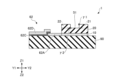
- FIG. FIG. 2 is a cross-sectional view (Part 1) showing the quantum bit according to the first embodiment.
- FIG. 3 is a cross-sectional view (Part 2) showing the quantum bit according to the first embodiment.
- FIG. 4 is a perspective view showing a higher-order topological insulator layer.
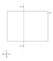
- FIG. 5 is a top view (No. 1) showing the method of manufacturing the quantum bit according to the first embodiment.
- FIG. 6 is a top view (Part 2) showing the method of manufacturing the quantum bit according to the first embodiment.
- FIG. 7 is a top view (No. 3) showing the method of manufacturing the quantum bit according to the first embodiment.
- FIG. 8 is a top view (No.
- FIG. 9 is a top view (No. 5) showing the method of manufacturing the quantum bit according to the first embodiment.
- FIG. 10 is a top view (No. 6) showing the method of manufacturing the quantum bit according to the first embodiment.
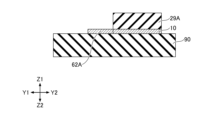
- FIG. 11 is a cross-sectional view (Part 1) showing the method of manufacturing the quantum bit according to the first embodiment.
- FIG. 12 is a cross-sectional view (Part 2) showing the method of manufacturing the quantum bit according to the first embodiment.
- FIG. 13 is a cross-sectional view (No. 3) showing the method of manufacturing the quantum bit according to the first embodiment.
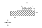
- FIG. 14 is a cross-sectional view (No. 4) showing the method of manufacturing the quantum bit according to the first embodiment.
- FIG. 15 is a cross-sectional view (No. 5) showing the method of manufacturing the quantum bit according to the first embodiment.
- FIG. 16 is a cross-sectional view (No. 6) showing the method of manufacturing the quantum bit according to the first embodiment.
- FIG. 17 is a diagram showing a quantum arithmetic device according to the second embodiment.
- the X1-X2 direction, the Y1-Y2 direction, and the Z1-Z2 direction are mutually orthogonal directions.
- a plane including the X1-X2 direction and the Y1-Y2 direction is referred to as the XY plane
- a plane including the Y1-Y2 direction and the Z1-Z2 direction is referred to as the YZ plane
- a plane including the Z1-Z2 direction and the X1-X2 direction. is described as the ZX plane.
- the Z1-Z2 direction is the vertical direction
- the Z1 side is the upper side
- the Z2 side is the lower side.
- the term “planar view” refers to viewing the object from the Z1 side
- the term “planar shape” refers to the shape of the object viewed from the Z1 side.
- FIG. 1 is a top view showing a quantum bit according to the first embodiment.
- FIG. 2 and 3 are cross-sectional views showing the quantum bit according to the first embodiment.
- FIG. 2 corresponds to a cross-sectional view taken along line II-II in FIG.
- FIG. 3 corresponds to a cross-sectional view taken along line III-III in FIG.
- the qubit 1 includes a substrate 90, an s-wave superconductor layer 10, a high-order topological insulator layer 20, a first ferromagnetic insulator layer 31, and a second ferromagnetic insulator layer. 32 and a third ferromagnetic insulator layer 33 .
- the quantum bit 1 further includes a first gate electrode 41, a second gate electrode 42, a third gate electrode 43, a first superconducting quantum interference device (SQUID) 61, a second SQUID 62, and a third SQUID 63 .
- SQUID superconducting quantum interference device
- the substrate 90 is, for example, a single crystal substrate whose surface has a Miller index of (100).
- Materials for substrate 90 include MgO, mica, sapphire, and SiC.
- the s-wave superconductor layer 10 is provided on part of the surface of the substrate 90 .
- the s-wave superconductor layer 10 is, for example, a Nb layer with a surface Miller index of (110).
- the thickness of the s-wave superconductor layer 10 is, for example, about 100 nm to 200 nm.
- the planar shape of the s-wave superconductor layer 10 is a rectangle having two sides parallel to the X1-X2 direction and two sides parallel to the Y1-Y2 direction.
- a high-order topological insulator layer 20 is provided on the s-wave superconductor layer 10 .
- Higher-order topological insulator layer 20 is, for example, multi-layer WTe 2 .
- multilayer WTe 2 has 5 to 100 layers, preferably 10 to 50 layers of WTe 2 which is a two-dimensional material. Since the thickness of a single layer of WTe 2 is 0.7 nm, the thickness of the high-order topological insulator layer 20 is about 10 nm when the high-order topological insulator layer 20 contains 14 layers of WTe 2 .
- FIG. 4 is a perspective view showing the high-order topological insulator layer 20.
- the shape of the high-order topological insulator layer 20 is a substantially rectangular parallelepiped.
- the a-axis direction of the high-order topological insulator layer 20 is parallel to the Y1-Y2 direction, the b-axis direction is parallel to the X1-X2 direction, and the c-axis direction is parallel to the Z1-Z2 direction.
- the Miller index of the top surface of the high-order topological insulator layer 20 is (001), the Miller index of the side surface on the Y2 side is (100), and the Miller index of the side surface on the X2 side is (010).
- a T-shaped groove 50 is formed in the surface of the high-order topological insulator layer 20 in plan view.
- the groove 50 has a first groove 51 , a second groove 52 and a third groove 53 .
- the width of the first groove 51, the second groove 52 and the third groove 53 is 20 nm, and the depth is 5 nm.
- the first groove 51 and the third groove 53 extend parallel to the X1-X2 direction, and the second groove 52 extends parallel to the Y1-Y2 direction.
- the first groove 51 is provided near the center of the high-order topological insulator layer 20 in the Y1-Y2 direction, and extends from the end of the high-order topological insulator layer 20 on the X2 side to the center in the X1-X2 direction.
- the third groove 53 is provided near the center of the high-order topological insulator layer 20 in the Y1-Y2 direction, and extends from the end of the high-order topological insulator layer 20 on the X1 side to the center in the X1-X2 direction. Therefore, the first groove 51 and the third groove 53 are formed in a straight line.
- the second groove 52 is provided near the center of the high-order topological insulator layer 20 in the X1-X2 direction and extends from the Y1-side end of the high-order topological insulator layer 20 to the center in the Y1-Y2 direction. Therefore, the second groove 52 is perpendicular to the first groove 51 and the third groove 53 .
- the high-order topological insulator layer 20 has the first region 21 on the Y2 side of the first groove 51 and the third groove 53 .
- the high-order topological insulator layer 20 has a second region 22 on the Y1 side of the first groove 51 and on the X2 side of the second groove 52 .
- the high-order topological insulator layer 20 has a third region 23 on the Y1 side of the third groove 53 and on the X1 side of the second groove 52 .
- Each of the first region 21, the second region 22 and the third region 23 has a hinge helical channel on one of two intersection lines of a plane perpendicular to the a-axis direction and a plane perpendicular to the c-axis direction.
- the hinge-helical channel is parallel to the b-axis.
- the first region 21 includes the first hinge helical channel 11 at the line of intersection (ridge line) between the top surface and the side surface on the Y1 side.
- the second region 22 has the second hinge helical channel 12 at the line of intersection between the side surface on the Y2 side and the bottom surface of the first groove 51 .
- the third region 23 has the third hinge helical channel 13 at the line of intersection between the side surface on the Y2 side and the bottom surface of the third groove 53 .
- the first hinge helical channel 11 is located at the line of intersection between the Y1 side surface of the first region 21 and the bottom surface of the groove 50
- the second hinge helical channel 12 is located between the upper surface of the second region 22 and the Y2 side surface. It may be on the line of intersection
- the third hinge-helical channel 13 may be on the line of intersection between the upper surface of the third region 23 and the side surface on the Y2 side.
- the first ferromagnetic insulator layer 31 is provided over part of the first region 21 , the second region 22 and the groove 50 and covers part of the first hinge helical channel 11 and the second hinge helical channel 12 . cover.
- a second ferromagnetic insulator layer 32 is provided over portions of the second region 22 , the third region 23 and the grooves 50 and partially overlies the second hinge helical channel 12 and the third hinge helical channel 13 . cover.
- a third ferromagnetic insulator layer 33 is provided over part of the third region 23 , the first region 21 and the groove 50 and covers part of the third hinge helical channel 13 and the first hinge helical channel 11 . cover.
- Examples of materials for the first ferromagnetic insulator layer 31, the second ferromagnetic insulator layer 32, and the third ferromagnetic insulator layer 33 include Cr2Ga2Te6 .
- the materials of the first ferromagnetic insulator layer 31, the second ferromagnetic insulator layer 32 and the third ferromagnetic insulator layer 33 may be other diluted magnetic semiconductors.
- the thicknesses of the first ferromagnetic insulator layer 31, the second ferromagnetic insulator layer 32, and the third ferromagnetic insulator layer 33 are, for example, about 30 nm.
- the second ferromagnetic insulator layer 32 is separated from the first ferromagnetic insulator layer 31 to the X1 side on the second hinge-helical channel 12 in the X1-X2 direction.
- the third ferromagnetic insulator layer 33 is separated from the second ferromagnetic insulator layer 32 to the X1 side on the third hinge-helical channel 13 in the X1-X2 direction.
- the third ferromagnetic insulator layer 33 is separated from the first ferromagnetic insulator layer 31 to the X1 side on the first hinge-helical channel 11 in the X1-X2 direction.
- the first gate electrode 41 is provided on the first ferromagnetic insulator layer 31 .
- a second gate electrode 42 is provided on the second ferromagnetic insulator layer 32 .
- a third gate electrode 43 is provided on the third ferromagnetic insulator layer 33 .
- Materials for the first gate electrode 41, the second gate electrode 42, and the third gate electrode 43 include Au.
- the thicknesses of the first gate electrode 41, the second gate electrode 42, and the third gate electrode 43 are, for example, about 100 nm.
- the first SQUID 61 has a lower superconductor layer 61A, a lower superconductor layer 61B, a tunnel barrier layer 61C, and an upper superconductor layer 61D.
- the lower superconductor layer 61A and the lower superconductor layer 61B protrude from the side surface of the s-wave superconductor layer 10 on the X2 side to the X2 side.
- the lower superconductor layer 61A is on the Y2 side of the lower superconductor layer 61B.
- the lower superconductor layer 61A protrudes from the first region 21 toward the X2 side
- the lower superconductor layer 61B protrudes from the second region 22 toward the X2 side.
- the lower superconductor layer 61 A and the lower superconductor layer 61 B are formed integrally with the s-wave superconductor layer 10 from the same material as the s-wave superconductor layer 10 .
- the lower superconductor layer 61 A and the lower superconductor layer 61 B are connected to the s-wave superconductor layer 10 .
- the lower superconductor layer 61A and the lower superconductor layer 61B are, for example, Nb layers with a thickness of about 100 nm to 200 nm.
- the tunnel barrier layer 61C and the upper superconductor layer 61D have a U-shaped planar shape.
- a material for the tunnel barrier layer 61C is NbOx
- a material for the upper superconductor layer 61D is Nb.
- the thickness of the tunnel barrier layer 61C is, for example, about 1 nm to 5 nm
- the thickness of the upper superconductor layer 61D is, for example, about 100 nm to 200 nm.
- One end of the tunnel barrier layer 61C contacts the lower superconductor layer 61A and the other end contacts the lower superconductor layer 61B.
- An upper superconductor layer 61D is provided on the tunnel barrier layer 61C.
- a tunnel barrier layer 61C is sandwiched between the lower superconductor layer 61A and the upper superconductor layer 61D and between the lower superconductor layer 61B and the upper superconductor layer 61D.
- the first SQUID 61 is composed of such a Josephson junction.
- the first SQUID 61 detects changes in magnetic flux between the first hinge helical channel 11 and the second hinge helical channel 12 .
- the second SQUID 62 has a lower superconductor layer 62A, a lower superconductor layer 62B, a tunnel barrier layer 62C, and an upper superconductor layer 62D.
- the lower superconductor layer 62A and the lower superconductor layer 62B protrude from the side surface of the s-wave superconductor layer 10 on the Y1 side to the Y1 side.
- the lower superconductor layer 62A is on the X2 side of the lower superconductor layer 62B.
- the lower superconductor layer 62A protrudes from the second region 22 toward the Y1 side
- the lower superconductor layer 62B protrudes from the third region 23 toward the Y1 side.
- the lower superconductor layer 62A and the lower superconductor layer 62B are formed integrally with the s-wave superconductor layer 10 from the same material as the s-wave superconductor layer 10.
- Lower superconductor layer 62 A and lower superconductor layer 62 B are connected to s-wave superconductor layer 10 .
- the lower superconductor layer 62A and the lower superconductor layer 62B are, for example, Nb layers with a thickness of about 100 nm to 200 nm.
- the tunnel barrier layer 62C and the upper superconductor layer 62D have a U-shaped planar shape.
- a material for the tunnel barrier layer 62C is NbOx
- a material for the upper superconductor layer 62D is Nb.
- the thickness of the tunnel barrier layer 62C is, for example, about 1 nm to 5 nm
- the thickness of the upper superconductor layer 62D is, for example, about 100 nm to 200 nm.
- One end of the tunnel barrier layer 62C contacts the lower superconductor layer 62A and the other end contacts the lower superconductor layer 62B.
- An upper superconductor layer 62D is provided over the tunnel barrier layer 62C.
- a tunnel barrier layer 62C is sandwiched between the lower superconductor layer 62A and the upper superconductor layer 62D and between the lower superconductor layer 62B and the upper superconductor layer 62D.
- the second SQUID 62 is composed of such a Josephson junction.
- the second SQUID 62 detects changes in magnetic flux between the second hinge-helical channel 12 and the third hinge-helical channel 13 .
- the third SQUID 63 has a lower superconductor layer 63A, a lower superconductor layer 63B, a tunnel barrier layer 63C, and an upper superconductor layer 63D.
- the lower superconductor layer 63A and the lower superconductor layer 63B protrude from the side surface of the s-wave superconductor layer 10 on the X1 side to the X1 side.
- the lower superconductor layer 63A is on the Y1 side of the lower superconductor layer 63B.
- the lower superconductor layer 63A protrudes from the third region 23 toward the X1 side
- the lower superconductor layer 63B protrudes from the first region 21 toward the X1 side.
- the lower superconductor layer 63 A and the lower superconductor layer 63 B are formed integrally with the s-wave superconductor layer 10 from the same material as the s-wave superconductor layer 10 .
- the lower superconductor layer 63 A and the lower superconductor layer 63 B are connected to the s-wave superconductor layer 10 .
- the lower superconductor layer 63A and the lower superconductor layer 63B are, for example, Nb layers with a thickness of about 100 nm to 200 nm.
- the tunnel barrier layer 63C and the upper superconductor layer 63D have a U-shaped planar shape.
- a material for the tunnel barrier layer 63C is NbOx
- a material for the upper superconductor layer 63D is Nb.
- the thickness of the tunnel barrier layer 63C is, for example, about 1 nm to 5 nm
- the thickness of the upper superconductor layer 63D is, for example, about 100 nm to 200 nm.
- One end of the tunnel barrier layer 63C contacts the lower superconductor layer 63A and the other end contacts the lower superconductor layer 63B.
- An upper superconductor layer 63D is provided on the tunnel barrier layer 63C.
- a tunnel barrier layer 63C is sandwiched between the lower superconductor layer 63A and the upper superconductor layer 63D and between the lower superconductor layer 63B and the upper superconductor layer 63D.
- the third SQUID 63 is composed of such a Josephson junction.
- the third SQUID 63 detects changes in magnetic flux between the third hinge helical channel 13 and the first hinge helical channel 11 .
- the Majorana particle ⁇ 1 is stably expressed near the first gate electrode 41 of the first hinge-helical channel 11
- the Majorana particle ⁇ 4 is stably expressed near the third gate electrode 43 of the first hinge-helical channel 11.
- the Majorana particle ⁇ 2 is stably expressed between the first gate electrode 41 and the second gate electrode 42 of the second hinge-helical channel 12
- the Majorana particle ⁇ 3 is stably expressed in the third hinge-helical channel 13. It is stably developed between the second gate electrode 42 and the third gate electrode 43 .
- Exchange of the Majorana particles ⁇ 1 to ⁇ 4 is carried out by a change in electrostatic potential caused by application of gate voltages to the first gate electrode 41, the second gate electrode 42, and the third gate electrode 43.
- the first gate electrode 41 when the Majorana particles ⁇ 1 and ⁇ 2 are exchanged, an electric field is applied from the first gate electrode 41, and the first SQUID 61 detects a minute change in magnetic flux as a minute change in voltage signal when the Majorana particles ⁇ 1 and ⁇ 2 are exchanged. detected.
- the second SQUID 62 detects minute changes in the magnetic flux during the exchange of the Majorana particles ⁇ 2 and ⁇ 3 as minute voltage signal changes.
- a monolayer film of WTe2 which is a layered material of transition metal dichalcogenide, is easily oxidized, and its properties change when exposed to the atmosphere. It is possible to suppress oxidation by sandwiching a single layer of WTe 2 between hexagonal boron nitride (h-BN), graphene, or other chemically stable substances. It complicates the process. It is also difficult to adjust the size of the WTe2 monolayer film.
- the high-order topological insulator layer 20 such as multilayer WTe 2 is used, a structure for suppressing oxidation is not required.
- adjusting the size of the high-order topological insulator layer 20 is easier than adjusting the size of a single layer film of WTe 2 .
- 5 to 10 are top views showing the manufacturing method of the quantum bit 1 according to the first embodiment.
- 11 to 16 are cross-sectional views showing the manufacturing method of the quantum bit 1 according to the first embodiment.
- FIGS. 5 and 11 corresponds to a cross-sectional view taken along line XI-XI in FIG.
- the s-wave superconductor layer 19 is formed on the substrate 90 , and the high-order topological insulator layer 29 is formed on the s-wave superconductor layer 19 .
- an Nb layer is formed as the s-wave superconductor layer 19 and a multi-layered WTe 2 is formed as the high-order topological insulator layer 29 .
- the s-wave superconductor layer 19 and the high-order topological insulator layer 29 can be epitaxially grown in situ in the same vacuum chamber, for example by pulse laser deposition (PLD).
- PLD pulse laser deposition
- the basic degree of vacuum when forming the s-wave superconductor layer 19 and the high-order topological insulator layer 29 is, for example, 5 ⁇ 10 ⁇ 6 Pa or less.
- the s-wave superconductor layer 19 and the high-order topological insulator layer 29 may be formed by, for example, a molecular beam epitaxy method, a sputtering method, a co-evaporation method, or the like.
- a Nb pure metal target can be used as the target.
- the temperature of the substrate 90 is maintained at about 400° C.
- the laser energy density is 2.0 J/cm 2 to 5.0 J/cm 2
- the irradiation frequency is 10 Hz.
- the distance between the substrate 90 and the target is about 5 cm
- the deposition rate is 0.5 nm/min to 1.0 nm/min.
- the Nb layer is epitaxially grown while being oriented in the [110] direction on the substrate 90 kept at about 400.degree.
- a WTe2 sintered body target can be used as the target.
- the temperature of the substrate 90 is maintained at 250° C. to 350° C.
- the laser energy density is 1.0 J/cm 2 to 2.0 J/cm 2
- the irradiation frequency is The frequency is 1 Hz
- the distance between the substrate 90 and the target is about 5 cm
- the deposition rate is 0.1 nm/min to 0.5 nm/min.
- the higher-order topological insulator layer 29 (multilayer WTe 2 ) is oriented in the c-axis direction on the s-wave superconductor layer 19 (Nb layer), and the crystal structure of the higher-order topological insulator layer 29 is the T d structure (space group : Pmm2 1 ).
- FIG. 12 corresponds to a cross-sectional view taken along line XII-XII in FIG.
- the high-order topological insulator layer 29 is spin-coated with a first electron beam resist.
- a first mask pattern is formed from the first electron beam resist.
- the first mask pattern is the s-wave superconductor layer 10, the lower superconductor layer 61A, the lower superconductor layer 61B, the lower superconductor layer 62A, and the lower superconductor layer 62B of the s-wave superconductor layer 19.
- the portion where the lower superconductor layer 63A and the lower superconductor layer 63B are to be formed are covered from above the high-order topological insulator layer 29, and other portions are exposed.
- the first electron beam resist for example, a resist obtained by diluting ZEP 520A (manufactured by Nippon Zeon Co., Ltd.) with ZEP-A (manufactured by Nippon Zeon Co., Ltd.) at a ratio of 1:1 can be used.
- the s-wave superconductor layer 19 and the high-order topological insulator layer 29 are processed by Ar ion milling.
- Ar ion milling for example, the beam acceleration voltage is 280 V and the beam current is 150 mA.
- FIG. 13 corresponds to a cross-sectional view taken along line XIII-XIII in FIG.
- the second electron beam resist is spin-coated on the high-order topological insulator layer 29 and the substrate 90 .
- a second mask pattern is formed from a second electron beam resist by electron beam lithography.
- the second mask pattern covers the portion of the high-order topological insulator layer 29 on the s-wave superconductor layer 10, the lower superconductor layer 61A, the lower superconductor layer 61B, the lower superconductor layer 62A, the lower superconductor layer 62A, and the lower superconductor layer 62A.
- the conductor layer 62B, the lower superconductor layer 63A and the upper portions of the lower superconductor layer 63B are exposed.
- the second electron beam resist for example, a resist obtained by diluting ZEP 520A (manufactured by Nippon Zeon Co., Ltd.) with ZEP-A (manufactured by Nippon Zeon Co., Ltd.) at a ratio of 1:1 can be used.
- the high-order topological insulator layer 29 is processed by Ar ion milling.
- a higher-order topological insulator layer 29A is formed, including a lower superconductor layer 61A, a lower superconductor layer 61B, a lower superconductor layer 62A, a lower superconductor layer 62B, a lower superconductor layer 63A and a lower superconductor layer 63A.
- Superconductor layer 63B is exposed from higher topological insulator layer 29A.
- the beam acceleration voltage is 280 V and the beam current is 150 mA.
- FIG. 14 corresponds to a cross-sectional view taken along line XIV-XIV in FIG.
- the high-order topological insulator layer 29A When processing the high-order topological insulator layer 29A, first, the high-order topological insulator layer 29A, the substrate 90, the lower superconductor layer 61A, the lower superconductor layer 61B, the lower superconductor layer 62A, the lower superconductor layer A third electron beam resist is spin-coated on the conductor layer 62B, the lower superconductor layer 63A and the lower superconductor layer 63B. Next, by electron beam lithography, a third mask pattern is formed from a third electron beam resist. The third mask pattern exposes the portion of the high-order topological insulator layer 29A where the trench 50 is to be formed and covers the other portion.
- the third electron beam resist for example, a resist obtained by diluting ZEP 520A (manufactured by Nippon Zeon Co., Ltd.) with ZEP-A (manufactured by Nippon Zeon Co., Ltd.) at a ratio of 1:1 can be used.
- the high-order topological insulator layer 29A is processed by Ar ion milling. As a result, a trench 50 comprising a first trench 51, a second trench 52 and a third trench 53 is formed, and a high-order topological insulator layer 20 comprising a first region 21, a second region 22 and a third region 23 is formed. is obtained.
- the first region 21 comprises the first hinge-helical channel 11
- the second region 22 comprises the second hinge-helical channel 12
- the third region 23 comprises the third hinge-helical channel 13 (see Figure 4).
- the beam acceleration voltage is 280 V and the beam current is 150 mA.
- FIG. 15 corresponds to a cross-sectional view taken along line XV-XV in FIG.
- the first ferromagnetic insulator layer 31 When forming the first ferromagnetic insulator layer 31, the second ferromagnetic insulator layer 32, the third ferromagnetic insulator layer 33, the first gate electrode 41, the second gate electrode 42 and the third gate electrode 43, First, the higher-order topological insulator layer 20, the substrate 90, the lower superconductor layer 61A, the lower superconductor layer 61B, the lower superconductor layer 62A, the lower superconductor layer 62B, the lower superconductor layer 63A and the lower A fourth electron beam resist is spin-coated on the superconductor layer 63B. Next, a fourth mask pattern is formed from a fourth electron beam resist by electron beam lithography.
- the fourth mask pattern includes a first ferromagnetic insulator layer 31, a second ferromagnetic insulator layer 32, a third ferromagnetic insulator layer 33, a first gate electrode 41, a second gate electrode 42 and a third gate electrode 43. It exposes the part that is to form the , and covers the other part.
- the fourth electron beam resist for example, a resist obtained by diluting ZEP 520A (manufactured by Nippon Zeon Co., Ltd.) with ZEP-A (manufactured by Nippon Zeon Co., Ltd.) at a ratio of 1:1 can be used.
- a Cr 2 Ga 2 Te 6 layer and an Au layer are formed by the PLD method.
- the temperature of the substrate 90 is maintained at 150° C. to 250° C. and the laser energy density is 1.0 J/cm 2 to 2.0 J/cm 2 .
- the irradiation frequency is 1 Hz
- the distance between the substrate 90 and the target is about 5 cm
- the deposition rate is 1.0 nm/min to 2.0 nm/min.
- the temperature of the substrate 90 is kept at room temperature, the laser energy density is 1.0 J/cm 2 to 2.0 J/cm 2 , the irradiation frequency is 5 Hz, and the substrate 90 is The distance from the target is about 5 cm, and the deposition rate is 5.0 nm/min to 10.0 nm/min.
- the fourth mask pattern is removed together with the Cr 2 Ga 2 Te 6 layer and the Au layer deposited thereon. That is, liftoff is performed.
- a first ferromagnetic insulator layer 31 a second ferromagnetic insulator layer 32, a third ferromagnetic insulator layer 33, a first gate electrode 41, a second gate electrode 42 and a third gate electrode 43 are obtained.
- four Majorana particles ⁇ 1, ⁇ 2, ⁇ 3 and ⁇ 4 are expressed.
- FIG. 16 corresponds to a cross-sectional view taken along line XVI-XVI in FIG.
- the tunnel barrier layers 61C-63C and the upper superconductor layers 61D-63D When forming the tunnel barrier layers 61C-63C and the upper superconductor layers 61D-63D, first, the higher-order topological insulator layer 20, the substrate 90, the lower superconductor layer 61A, the lower superconductor layer 61B, the lower fifth electrons on superconductor layer 62A, lower superconductor layer 62B, lower superconductor layer 63A, lower superconductor layer 63B, first gate electrode 41, second gate electrode 42 and third gate electrode 43; Spin coat the line resist. Next, by electron beam lithography, a fifth mask pattern is formed from a fifth electron beam resist.
- the fifth mask pattern exposes portions where the tunnel barrier layers 61C-63C and upper superconductor layers 61D-63D are to be formed, and covers other portions.
- the fifth electron beam resist for example, a resist obtained by diluting ZEP 520A (manufactured by Nippon Zeon Co., Ltd.) with ZEP-A (manufactured by Nippon Zeon Co., Ltd.) at a ratio of 1:1 can be used.
- an NbOx layer and an Nb layer are formed by the PLD method.
- the temperature of the substrate 90 is maintained at room temperature, and the oxygen partial pressure in the vacuum chamber is adjusted to about 50 Pa to 55 Pa.
- the Nb layer can be formed under the same conditions as the s-wave superconductor layer 19 .
- the fifth mask pattern is removed together with the NbOx and Nb layers deposited thereon. That is, liftoff is performed. As a result, tunnel barrier layers 61C-63C and upper superconductor layers 61D-63D are obtained, and a first SQUID 61, a second SQUID 62 and a third SQUID 63 are formed.
- the quantum bit 1 according to the first embodiment can be manufactured.
- the material of the higher topological insulator layer 20 is not limited to multi-layer WTe2 , but may be multi-layer Bi4Br4 , for example. Also, the material of the s-wave superconductor layer 10 is not limited to Nb, and may be Al or Pd, for example.
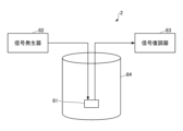
- FIG. 17 is a diagram showing a quantum arithmetic device according to the second embodiment.
- the quantum arithmetic device 2 has a quantum bit chip 81, a signal generator 82, a signal demodulator 83, and a cryogenic dilution refrigerator 84, as shown in FIG.
- a qubit chip 81 includes a plurality of qubits 1 according to the first embodiment.
- a qubit chip 81 is housed in a cryogenic dilution refrigerator 84 and cooled to a temperature of 10 mK or less.
- a signal generator 82 generates a microwave pulse signal, and the microwave pulse signal is input to the qubit chip 81 .
- the quantum bit chip 81 outputs a signal corresponding to the microwave pulse signal, and the signal demodulator 83 demodulates the signal output from the quantum bit chip 81 .
- the signal generator 82 and signal demodulator 83 are used, for example, at room temperature.
- the quantum arithmetic device 2 according to the second embodiment includes the quantum bit 1 according to the first embodiment, the Majorana particles can be stably expressed, and stable computation can be performed.
- Quantum bit 2 Quantum arithmetic device 10: s-wave superconductor layer 11: First hinge helical channel 12: Second hinge helical channel 13: Third hinge helical channel 20: Higher order topological insulator layer 21: First Region 22: Second region 23: Third region 31: First ferromagnetic insulator layer 32: Second ferromagnetic insulator layer 33: Third ferromagnetic insulator layer 41: First gate electrode 42: Second gate electrode 43: Third gate electrode 50: Groove 51: First groove 52: Second groove 53: Third groove 61: First SQUID 62: Second SQUID 63: Third SQUID
Landscapes
- Superconductor Devices And Manufacturing Methods Thereof (AREA)
Priority Applications (2)
| Application Number | Priority Date | Filing Date | Title |
|---|---|---|---|
| JP2023549195A JP7666617B2 (ja) | 2021-09-21 | 2021-09-21 | 量子ビット、量子演算装置及び量子ビットの製造方法 |
| PCT/JP2021/034578 WO2023047461A1 (ja) | 2021-09-21 | 2021-09-21 | 量子ビット、量子演算装置及び量子ビットの製造方法 |
Applications Claiming Priority (1)
| Application Number | Priority Date | Filing Date | Title |
|---|---|---|---|
| PCT/JP2021/034578 WO2023047461A1 (ja) | 2021-09-21 | 2021-09-21 | 量子ビット、量子演算装置及び量子ビットの製造方法 |
Publications (2)
| Publication Number | Publication Date |
|---|---|
| WO2023047461A1 true WO2023047461A1 (ja) | 2023-03-30 |
| WO2023047461A9 WO2023047461A9 (ja) | 2024-02-08 |
Family
ID=85720255
Family Applications (1)
| Application Number | Title | Priority Date | Filing Date |
|---|---|---|---|
| PCT/JP2021/034578 Ceased WO2023047461A1 (ja) | 2021-09-21 | 2021-09-21 | 量子ビット、量子演算装置及び量子ビットの製造方法 |
Country Status (2)
| Country | Link |
|---|---|
| JP (1) | JP7666617B2 (https=) |
| WO (1) | WO2023047461A1 (https=) |
Families Citing this family (1)
| Publication number | Priority date | Publication date | Assignee | Title |
|---|---|---|---|---|
| JPWO2023181247A1 (https=) * | 2022-03-24 | 2023-09-28 |
Citations (2)
| Publication number | Priority date | Publication date | Assignee | Title |
|---|---|---|---|---|
| JP2020511780A (ja) * | 2017-03-20 | 2020-04-16 | フォルシュングスツェントルム・ユーリッヒ・ゲゼルシャフト・ミット・ベシュレンクテル・ハフツング | マヨラナ材料と超伝導体のハイブリッド網構造のインサイチュによる製造方法及びその方法により製造されたハイブリッド構造 |
| JP2020096107A (ja) * | 2018-12-13 | 2020-06-18 | 株式会社日立製作所 | 量子ビット及びその制御方法 |
-
2021
- 2021-09-21 WO PCT/JP2021/034578 patent/WO2023047461A1/ja not_active Ceased
- 2021-09-21 JP JP2023549195A patent/JP7666617B2/ja active Active
Patent Citations (2)
| Publication number | Priority date | Publication date | Assignee | Title |
|---|---|---|---|---|
| JP2020511780A (ja) * | 2017-03-20 | 2020-04-16 | フォルシュングスツェントルム・ユーリッヒ・ゲゼルシャフト・ミット・ベシュレンクテル・ハフツング | マヨラナ材料と超伝導体のハイブリッド網構造のインサイチュによる製造方法及びその方法により製造されたハイブリッド構造 |
| JP2020096107A (ja) * | 2018-12-13 | 2020-06-18 | 株式会社日立製作所 | 量子ビット及びその制御方法 |
Non-Patent Citations (2)
| Title |
|---|
| FEI ZAIYAO, PALOMAKI TAUNO, WU SANFENG, ZHAO WENJIN, CAI XINGHAN, SUN BOSONG, NGUYEN PAUL, FINNEY JOSEPH, XU XIAODONG, COBDEN DAVI: "Edge conduction in monolayer WTe2", NATURE PHYSICS, NATURE PUBLISHING GROUP, LONDON, GB, vol. 13, no. 7, 1 July 2017 (2017-07-01), GB , pages 677 - 682, XP093053561, ISSN: 1745-2473, DOI: 10.1038/nphys4091 * |
| HSU CHEN-HSUAN, STANO PETER, KLINOVAJA JELENA, LOSS DANIEL: "Majorana Kramers Pairs in Higher-Order Topological Insulators", PHYSICAL REVIEW LETTERS, AMERICAN PHYSICAL SOCIETY, US, vol. 121, no. 19, 1 November 2018 (2018-11-01), US , XP093053563, ISSN: 0031-9007, DOI: 10.1103/PhysRevLett.121.196801 * |
Also Published As
| Publication number | Publication date |
|---|---|
| JP7666617B2 (ja) | 2025-04-22 |
| WO2023047461A9 (ja) | 2024-02-08 |
| JPWO2023047461A1 (https=) | 2023-03-30 |
Similar Documents
| Publication | Publication Date | Title |
|---|---|---|
| US20030042481A1 (en) | Trilayer heterostructure josephson junctions | |
| US20030107033A1 (en) | Trilayer heterostructure junctions | |
| Kneiß et al. | Suppression of Grain Boundary Scattering in Multifunctional p‐Type Transparent γ‐CuI Thin Films due to Interface Tunneling Currents | |
| JP2025135013A (ja) | 量子ビット及び量子演算装置 | |
| CN106784279A (zh) | 一种高性能掺杂钛酸锶氧化物热电薄膜的制备方法 | |
| WO2022137421A1 (ja) | 量子ビット回路、量子コンピュータ及び量子ビット回路の製造方法 | |
| JP7666617B2 (ja) | 量子ビット、量子演算装置及び量子ビットの製造方法 | |
| JP2016097599A (ja) | 層状物質の積層構造及びその製造方法 | |
| JP2006237304A (ja) | 強磁性伝導体材料およびその製造方法、並びに磁気抵抗素子、電界効果トランジスタ | |
| WO2024023967A1 (ja) | 構造体、量子ビット、量子演算装置及び構造体の製造方法 | |
| JP2009302219A (ja) | 超伝導配線構造 | |
| WO2018100837A1 (ja) | 磁化反転素子、磁気抵抗効果素子、集積素子及び集積素子の製造方法 | |
| WO2024127469A1 (ja) | 積層構造体、量子ビットデバイス、積層構造体の製造方法及び量子ビットデバイスの製造方法 | |
| JP7698225B2 (ja) | トポロジカル絶縁体、量子ビット、トポロジカル絶縁体の製造方法、および量子ビットの製造方法 | |
| JP2025129796A (ja) | 構造体、量子ビット、量子演算装置、構造体の製造方法及び量子ビットの製造方法 | |
| JP2024017592A (ja) | 電子スピン伝送素子、発光装置、発光アレイ装置及びセンサ装置 | |
| JP7679884B2 (ja) | マヨラナ量子ビット及び量子コンピュータ | |
| JP4818614B2 (ja) | 超電導積層体およびその製造方法、ジョセフソン接合素子、電子装置 | |
| JP4795671B2 (ja) | 超伝導体積層構造及びその作製方法 | |
| JP3186035B2 (ja) | 電界効果素子用積層薄膜および該積層薄膜を用いた電界効果トランジスター | |
| JPH0278282A (ja) | ジヨセフソン素子 | |
| JP2786827B2 (ja) | 超電導素子 | |
| Stepantsov | Growth of YBa2Cu3O7 Films with a Packet of Parallel Grain Boundaries Spaced by Nanometer Distances | |
| JP5054463B2 (ja) | ジョセフソン接合素子、その形成方法、および超電導接合回路 | |
| Satoh | A potential in thermoelectric oxide phononic crystal |
Legal Events
| Date | Code | Title | Description |
|---|---|---|---|
| WWE | Wipo information: entry into national phase |
Ref document number: 2023549195 Country of ref document: JP |
|
| NENP | Non-entry into the national phase |
Ref country code: DE |
|
| 122 | Ep: pct application non-entry in european phase |
Ref document number: 21958338 Country of ref document: EP Kind code of ref document: A1 |