WO2023042022A1 - Dispositif à semi-conducteurs et dispositif de stockage - Google Patents
Dispositif à semi-conducteurs et dispositif de stockage Download PDFInfo
- Publication number
- WO2023042022A1 WO2023042022A1 PCT/IB2022/058239 IB2022058239W WO2023042022A1 WO 2023042022 A1 WO2023042022 A1 WO 2023042022A1 IB 2022058239 W IB2022058239 W IB 2022058239W WO 2023042022 A1 WO2023042022 A1 WO 2023042022A1
- Authority
- WO
- WIPO (PCT)
- Prior art keywords
- conductor
- insulator
- oxide
- transistor
- semiconductor device
- Prior art date
Links
- 239000004065 semiconductor Substances 0.000 title claims abstract description 322
- 238000003860 storage Methods 0.000 title claims description 50
- 239000004020 conductor Substances 0.000 claims abstract description 801
- 239000012212 insulator Substances 0.000 claims abstract description 692
- 229910044991 metal oxide Inorganic materials 0.000 claims abstract description 91
- 150000004706 metal oxides Chemical class 0.000 claims abstract description 90
- 230000010354 integration Effects 0.000 abstract description 4
- 239000010408 film Substances 0.000 description 362
- 238000000034 method Methods 0.000 description 198
- 239000010410 layer Substances 0.000 description 159
- IJGRMHOSHXDMSA-UHFFFAOYSA-N Atomic nitrogen Chemical compound N#N IJGRMHOSHXDMSA-UHFFFAOYSA-N 0.000 description 137
- 229910052760 oxygen Inorganic materials 0.000 description 125
- 239000001301 oxygen Substances 0.000 description 125
- QVGXLLKOCUKJST-UHFFFAOYSA-N atomic oxygen Chemical compound [O] QVGXLLKOCUKJST-UHFFFAOYSA-N 0.000 description 122
- 239000000758 substrate Substances 0.000 description 120
- 230000006870 function Effects 0.000 description 119
- 239000000463 material Substances 0.000 description 72
- 238000004544 sputter deposition Methods 0.000 description 72
- 230000015654 memory Effects 0.000 description 67
- 229910052739 hydrogen Inorganic materials 0.000 description 66
- 239000001257 hydrogen Substances 0.000 description 66
- 229910052757 nitrogen Inorganic materials 0.000 description 64
- UFHFLCQGNIYNRP-UHFFFAOYSA-N Hydrogen Chemical compound [H][H] UFHFLCQGNIYNRP-UHFFFAOYSA-N 0.000 description 63
- 230000015572 biosynthetic process Effects 0.000 description 60
- 150000004767 nitrides Chemical class 0.000 description 57
- 239000012535 impurity Substances 0.000 description 54
- 229910052782 aluminium Inorganic materials 0.000 description 51
- 238000000231 atomic layer deposition Methods 0.000 description 51
- 229910052715 tantalum Inorganic materials 0.000 description 50
- GUVRBAGPIYLISA-UHFFFAOYSA-N tantalum atom Chemical compound [Ta] GUVRBAGPIYLISA-UHFFFAOYSA-N 0.000 description 50
- XAGFODPZIPBFFR-UHFFFAOYSA-N aluminium Chemical compound [Al] XAGFODPZIPBFFR-UHFFFAOYSA-N 0.000 description 49
- 239000013078 crystal Substances 0.000 description 48
- XUIMIQQOPSSXEZ-UHFFFAOYSA-N Silicon Chemical compound [Si] XUIMIQQOPSSXEZ-UHFFFAOYSA-N 0.000 description 46
- 229910052710 silicon Inorganic materials 0.000 description 46
- 239000010703 silicon Substances 0.000 description 46
- VYPSYNLAJGMNEJ-UHFFFAOYSA-N Silicium dioxide Chemical compound O=[Si]=O VYPSYNLAJGMNEJ-UHFFFAOYSA-N 0.000 description 45
- 239000003990 capacitor Substances 0.000 description 44
- 229910052735 hafnium Inorganic materials 0.000 description 43
- 238000004519 manufacturing process Methods 0.000 description 41
- VBJZVLUMGGDVMO-UHFFFAOYSA-N hafnium atom Chemical compound [Hf] VBJZVLUMGGDVMO-UHFFFAOYSA-N 0.000 description 40
- 229910052814 silicon oxide Inorganic materials 0.000 description 40
- 238000010438 heat treatment Methods 0.000 description 38
- 239000007789 gas Substances 0.000 description 37
- 238000005229 chemical vapour deposition Methods 0.000 description 35
- 229910052581 Si3N4 Inorganic materials 0.000 description 33
- 229910052751 metal Inorganic materials 0.000 description 33
- HQVNEWCFYHHQES-UHFFFAOYSA-N silicon nitride Chemical compound N12[Si]34N5[Si]62N3[Si]51N64 HQVNEWCFYHHQES-UHFFFAOYSA-N 0.000 description 33
- 239000011701 zinc Substances 0.000 description 33
- 239000002184 metal Substances 0.000 description 30
- 238000012545 processing Methods 0.000 description 30
- 229910052738 indium Inorganic materials 0.000 description 28
- 238000009792 diffusion process Methods 0.000 description 26
- APFVFJFRJDLVQX-UHFFFAOYSA-N indium atom Chemical compound [In] APFVFJFRJDLVQX-UHFFFAOYSA-N 0.000 description 25
- 239000010936 titanium Substances 0.000 description 25
- XLYOFNOQVPJJNP-UHFFFAOYSA-N water Substances O XLYOFNOQVPJJNP-UHFFFAOYSA-N 0.000 description 25
- 229910001868 water Inorganic materials 0.000 description 25
- RTAQQCXQSZGOHL-UHFFFAOYSA-N Titanium Chemical compound [Ti] RTAQQCXQSZGOHL-UHFFFAOYSA-N 0.000 description 24
- 229910052719 titanium Inorganic materials 0.000 description 24
- 238000005530 etching Methods 0.000 description 22
- OKTJSMMVPCPJKN-UHFFFAOYSA-N Carbon Chemical compound [C] OKTJSMMVPCPJKN-UHFFFAOYSA-N 0.000 description 21
- 239000012298 atmosphere Substances 0.000 description 21
- 239000000203 mixture Substances 0.000 description 21
- 229910052721 tungsten Inorganic materials 0.000 description 21
- 239000010937 tungsten Substances 0.000 description 21
- PXHVJJICTQNCMI-UHFFFAOYSA-N Nickel Chemical compound [Ni] PXHVJJICTQNCMI-UHFFFAOYSA-N 0.000 description 20
- 229910052799 carbon Inorganic materials 0.000 description 20
- WFKWXMTUELFFGS-UHFFFAOYSA-N tungsten Chemical compound [W] WFKWXMTUELFFGS-UHFFFAOYSA-N 0.000 description 20
- 230000008569 process Effects 0.000 description 19
- 238000004549 pulsed laser deposition Methods 0.000 description 19
- 229910052733 gallium Inorganic materials 0.000 description 18
- 238000001451 molecular beam epitaxy Methods 0.000 description 18
- 125000004429 atom Chemical group 0.000 description 17
- -1 element M Chemical compound 0.000 description 17
- 238000000059 patterning Methods 0.000 description 17
- 230000007547 defect Effects 0.000 description 16
- 238000001312 dry etching Methods 0.000 description 16
- 229910052707 ruthenium Inorganic materials 0.000 description 16
- NRTOMJZYCJJWKI-UHFFFAOYSA-N Titanium nitride Chemical compound [Ti]#N NRTOMJZYCJJWKI-UHFFFAOYSA-N 0.000 description 15
- TWNQGVIAIRXVLR-UHFFFAOYSA-N oxo(oxoalumanyloxy)alumane Chemical compound O=[Al]O[Al]=O TWNQGVIAIRXVLR-UHFFFAOYSA-N 0.000 description 15
- 239000002356 single layer Substances 0.000 description 15
- XKRFYHLGVUSROY-UHFFFAOYSA-N Argon Chemical compound [Ar] XKRFYHLGVUSROY-UHFFFAOYSA-N 0.000 description 14
- RYGMFSIKBFXOCR-UHFFFAOYSA-N Copper Chemical group [Cu] RYGMFSIKBFXOCR-UHFFFAOYSA-N 0.000 description 14
- GYHNNYVSQQEPJS-UHFFFAOYSA-N Gallium Chemical compound [Ga] GYHNNYVSQQEPJS-UHFFFAOYSA-N 0.000 description 14
- 238000004140 cleaning Methods 0.000 description 14
- MWUXSHHQAYIFBG-UHFFFAOYSA-N Nitric oxide Chemical compound O=[N] MWUXSHHQAYIFBG-UHFFFAOYSA-N 0.000 description 12
- KJTLSVCANCCWHF-UHFFFAOYSA-N Ruthenium Chemical compound [Ru] KJTLSVCANCCWHF-UHFFFAOYSA-N 0.000 description 12
- 238000002441 X-ray diffraction Methods 0.000 description 12
- 238000010586 diagram Methods 0.000 description 12
- 229910001882 dioxygen Inorganic materials 0.000 description 12
- 229910000449 hafnium oxide Inorganic materials 0.000 description 12
- WIHZLLGSGQNAGK-UHFFFAOYSA-N hafnium(4+);oxygen(2-) Chemical compound [O-2].[O-2].[Hf+4] WIHZLLGSGQNAGK-UHFFFAOYSA-N 0.000 description 12
- MYMOFIZGZYHOMD-UHFFFAOYSA-N Dioxygen Chemical compound O=O MYMOFIZGZYHOMD-UHFFFAOYSA-N 0.000 description 11
- KRHYYFGTRYWZRS-UHFFFAOYSA-N Fluorane Chemical compound F KRHYYFGTRYWZRS-UHFFFAOYSA-N 0.000 description 11
- 229910001873 dinitrogen Inorganic materials 0.000 description 11
- 239000011229 interlayer Substances 0.000 description 11
- 238000007254 oxidation reaction Methods 0.000 description 11
- 230000002093 peripheral effect Effects 0.000 description 11
- 239000011347 resin Substances 0.000 description 11
- 229920005989 resin Polymers 0.000 description 11
- 238000001039 wet etching Methods 0.000 description 11
- 229910052725 zinc Inorganic materials 0.000 description 11
- PXGOKWXKJXAPGV-UHFFFAOYSA-N Fluorine Chemical compound FF PXGOKWXKJXAPGV-UHFFFAOYSA-N 0.000 description 10
- ZOKXTWBITQBERF-UHFFFAOYSA-N Molybdenum Chemical compound [Mo] ZOKXTWBITQBERF-UHFFFAOYSA-N 0.000 description 10
- 230000004888 barrier function Effects 0.000 description 10
- 229910052802 copper Inorganic materials 0.000 description 10
- 239000010949 copper Substances 0.000 description 10
- 230000000694 effects Effects 0.000 description 10
- 239000011737 fluorine Substances 0.000 description 10
- 229910052731 fluorine Inorganic materials 0.000 description 10
- 229910052746 lanthanum Inorganic materials 0.000 description 10
- FZLIPJUXYLNCLC-UHFFFAOYSA-N lanthanum atom Chemical compound [La] FZLIPJUXYLNCLC-UHFFFAOYSA-N 0.000 description 10
- 230000004048 modification Effects 0.000 description 10
- 238000012986 modification Methods 0.000 description 10
- 229910052750 molybdenum Inorganic materials 0.000 description 10
- 239000011733 molybdenum Substances 0.000 description 10
- 229910052759 nickel Inorganic materials 0.000 description 10
- 230000003647 oxidation Effects 0.000 description 10
- RVTZCBVAJQQJTK-UHFFFAOYSA-N oxygen(2-);zirconium(4+) Chemical compound [O-2].[O-2].[Zr+4] RVTZCBVAJQQJTK-UHFFFAOYSA-N 0.000 description 10
- 229910001928 zirconium oxide Inorganic materials 0.000 description 10
- 238000010894 electron beam technology Methods 0.000 description 9
- 229910001925 ruthenium oxide Inorganic materials 0.000 description 9
- WOCIAKWEIIZHES-UHFFFAOYSA-N ruthenium(iv) oxide Chemical compound O=[Ru]=O WOCIAKWEIIZHES-UHFFFAOYSA-N 0.000 description 9
- MZLGASXMSKOWSE-UHFFFAOYSA-N tantalum nitride Chemical compound [Ta]#N MZLGASXMSKOWSE-UHFFFAOYSA-N 0.000 description 9
- 238000000151 deposition Methods 0.000 description 8
- 230000008021 deposition Effects 0.000 description 8
- 238000005516 engineering process Methods 0.000 description 8
- 239000000126 substance Substances 0.000 description 8
- JBQYATWDVHIOAR-UHFFFAOYSA-N tellanylidenegermanium Chemical compound [Te]=[Ge] JBQYATWDVHIOAR-UHFFFAOYSA-N 0.000 description 8
- 229910052786 argon Inorganic materials 0.000 description 7
- 238000013461 design Methods 0.000 description 7
- 239000002243 precursor Substances 0.000 description 7
- 238000001004 secondary ion mass spectrometry Methods 0.000 description 7
- 238000001228 spectrum Methods 0.000 description 7
- 239000010409 thin film Substances 0.000 description 7
- ZOXJGFHDIHLPTG-UHFFFAOYSA-N Boron Chemical compound [B] ZOXJGFHDIHLPTG-UHFFFAOYSA-N 0.000 description 6
- XEEYBQQBJWHFJM-UHFFFAOYSA-N Iron Chemical compound [Fe] XEEYBQQBJWHFJM-UHFFFAOYSA-N 0.000 description 6
- FYYHWMGAXLPEAU-UHFFFAOYSA-N Magnesium Chemical compound [Mg] FYYHWMGAXLPEAU-UHFFFAOYSA-N 0.000 description 6
- OAICVXFJPJFONN-UHFFFAOYSA-N Phosphorus Chemical compound [P] OAICVXFJPJFONN-UHFFFAOYSA-N 0.000 description 6
- HCHKCACWOHOZIP-UHFFFAOYSA-N Zinc Chemical compound [Zn] HCHKCACWOHOZIP-UHFFFAOYSA-N 0.000 description 6
- XLOMVQKBTHCTTD-UHFFFAOYSA-N Zinc monoxide Chemical compound [Zn]=O XLOMVQKBTHCTTD-UHFFFAOYSA-N 0.000 description 6
- QCWXUUIWCKQGHC-UHFFFAOYSA-N Zirconium Chemical compound [Zr] QCWXUUIWCKQGHC-UHFFFAOYSA-N 0.000 description 6
- 229910052796 boron Inorganic materials 0.000 description 6
- 239000003795 chemical substances by application Substances 0.000 description 6
- AJNVQOSZGJRYEI-UHFFFAOYSA-N digallium;oxygen(2-) Chemical compound [O-2].[O-2].[O-2].[Ga+3].[Ga+3] AJNVQOSZGJRYEI-UHFFFAOYSA-N 0.000 description 6
- 230000005669 field effect Effects 0.000 description 6
- 229910001195 gallium oxide Inorganic materials 0.000 description 6
- 229910052732 germanium Inorganic materials 0.000 description 6
- GNPVGFCGXDBREM-UHFFFAOYSA-N germanium atom Chemical compound [Ge] GNPVGFCGXDBREM-UHFFFAOYSA-N 0.000 description 6
- 229910052749 magnesium Inorganic materials 0.000 description 6
- 239000011777 magnesium Substances 0.000 description 6
- 239000011574 phosphorus Substances 0.000 description 6
- 229910052698 phosphorus Inorganic materials 0.000 description 6
- 229910052712 strontium Inorganic materials 0.000 description 6
- CIOAGBVUUVVLOB-UHFFFAOYSA-N strontium atom Chemical compound [Sr] CIOAGBVUUVVLOB-UHFFFAOYSA-N 0.000 description 6
- 229910052726 zirconium Inorganic materials 0.000 description 6
- VHUUQVKOLVNVRT-UHFFFAOYSA-N Ammonium hydroxide Chemical compound [NH4+].[OH-] VHUUQVKOLVNVRT-UHFFFAOYSA-N 0.000 description 5
- 229910052784 alkaline earth metal Inorganic materials 0.000 description 5
- 235000011114 ammonium hydroxide Nutrition 0.000 description 5
- 239000007864 aqueous solution Substances 0.000 description 5
- 238000003491 array Methods 0.000 description 5
- 239000000969 carrier Substances 0.000 description 5
- 239000000460 chlorine Substances 0.000 description 5
- 230000002349 favourable effect Effects 0.000 description 5
- 229910003437 indium oxide Inorganic materials 0.000 description 5
- PJXISJQVUVHSOJ-UHFFFAOYSA-N indium(iii) oxide Chemical compound [O-2].[O-2].[O-2].[In+3].[In+3] PJXISJQVUVHSOJ-UHFFFAOYSA-N 0.000 description 5
- 238000001459 lithography Methods 0.000 description 5
- 230000001590 oxidative effect Effects 0.000 description 5
- 125000004430 oxygen atom Chemical group O* 0.000 description 5
- 239000000376 reactant Substances 0.000 description 5
- 238000002230 thermal chemical vapour deposition Methods 0.000 description 5
- 229910052727 yttrium Inorganic materials 0.000 description 5
- VWQVUPCCIRVNHF-UHFFFAOYSA-N yttrium atom Chemical compound [Y] VWQVUPCCIRVNHF-UHFFFAOYSA-N 0.000 description 5
- ZAMOUSCENKQFHK-UHFFFAOYSA-N Chlorine atom Chemical compound [Cl] ZAMOUSCENKQFHK-UHFFFAOYSA-N 0.000 description 4
- 229910052779 Neodymium Inorganic materials 0.000 description 4
- 229910000577 Silicon-germanium Inorganic materials 0.000 description 4
- LEVVHYCKPQWKOP-UHFFFAOYSA-N [Si].[Ge] Chemical compound [Si].[Ge] LEVVHYCKPQWKOP-UHFFFAOYSA-N 0.000 description 4
- 229910052783 alkali metal Inorganic materials 0.000 description 4
- 150000001340 alkali metals Chemical class 0.000 description 4
- 150000001342 alkaline earth metals Chemical class 0.000 description 4
- 239000000956 alloy Substances 0.000 description 4
- 229910052801 chlorine Inorganic materials 0.000 description 4
- 150000001875 compounds Chemical class 0.000 description 4
- 238000001341 grazing-angle X-ray diffraction Methods 0.000 description 4
- 125000004435 hydrogen atom Chemical group [H]* 0.000 description 4
- AMGQUBHHOARCQH-UHFFFAOYSA-N indium;oxotin Chemical compound [In].[Sn]=O AMGQUBHHOARCQH-UHFFFAOYSA-N 0.000 description 4
- MRELNEQAGSRDBK-UHFFFAOYSA-N lanthanum(3+);oxygen(2-) Chemical compound [O-2].[O-2].[O-2].[La+3].[La+3] MRELNEQAGSRDBK-UHFFFAOYSA-N 0.000 description 4
- 239000007788 liquid Substances 0.000 description 4
- 238000005259 measurement Methods 0.000 description 4
- 239000002159 nanocrystal Substances 0.000 description 4
- QEFYFXOXNSNQGX-UHFFFAOYSA-N neodymium atom Chemical compound [Nd] QEFYFXOXNSNQGX-UHFFFAOYSA-N 0.000 description 4
- PLDDOISOJJCEMH-UHFFFAOYSA-N neodymium(3+);oxygen(2-) Chemical compound [O-2].[O-2].[O-2].[Nd+3].[Nd+3] PLDDOISOJJCEMH-UHFFFAOYSA-N 0.000 description 4
- 125000004433 nitrogen atom Chemical group N* 0.000 description 4
- 230000003071 parasitic effect Effects 0.000 description 4
- BASFCYQUMIYNBI-UHFFFAOYSA-N platinum Chemical compound [Pt] BASFCYQUMIYNBI-UHFFFAOYSA-N 0.000 description 4
- 230000009467 reduction Effects 0.000 description 4
- JBRZTFJDHDCESZ-UHFFFAOYSA-N AsGa Chemical compound [As]#[Ga] JBRZTFJDHDCESZ-UHFFFAOYSA-N 0.000 description 3
- 229910001218 Gallium arsenide Inorganic materials 0.000 description 3
- BPQQTUXANYXVAA-UHFFFAOYSA-N Orthosilicate Chemical compound [O-][Si]([O-])([O-])[O-] BPQQTUXANYXVAA-UHFFFAOYSA-N 0.000 description 3
- MUBZPKHOEPUJKR-UHFFFAOYSA-N Oxalic acid Chemical compound OC(=O)C(O)=O MUBZPKHOEPUJKR-UHFFFAOYSA-N 0.000 description 3
- ATJFFYVFTNAWJD-UHFFFAOYSA-N Tin Chemical compound [Sn] ATJFFYVFTNAWJD-UHFFFAOYSA-N 0.000 description 3
- GWEVSGVZZGPLCZ-UHFFFAOYSA-N Titan oxide Chemical compound O=[Ti]=O GWEVSGVZZGPLCZ-UHFFFAOYSA-N 0.000 description 3
- 238000004833 X-ray photoelectron spectroscopy Methods 0.000 description 3
- 229910045601 alloy Inorganic materials 0.000 description 3
- 238000006243 chemical reaction Methods 0.000 description 3
- 238000004891 communication Methods 0.000 description 3
- 239000000470 constituent Substances 0.000 description 3
- 238000007865 diluting Methods 0.000 description 3
- 238000002003 electron diffraction Methods 0.000 description 3
- 238000007667 floating Methods 0.000 description 3
- 125000005843 halogen group Chemical group 0.000 description 3
- 150000002431 hydrogen Chemical class 0.000 description 3
- 239000011261 inert gas Substances 0.000 description 3
- 229910052742 iron Inorganic materials 0.000 description 3
- CPLXHLVBOLITMK-UHFFFAOYSA-N magnesium oxide Inorganic materials [Mg]=O CPLXHLVBOLITMK-UHFFFAOYSA-N 0.000 description 3
- 239000000395 magnesium oxide Substances 0.000 description 3
- AXZKOIWUVFPNLO-UHFFFAOYSA-N magnesium;oxygen(2-) Chemical compound [O-2].[Mg+2] AXZKOIWUVFPNLO-UHFFFAOYSA-N 0.000 description 3
- 239000011159 matrix material Substances 0.000 description 3
- QGLKJKCYBOYXKC-UHFFFAOYSA-N nonaoxidotritungsten Chemical compound O=[W]1(=O)O[W](=O)(=O)O[W](=O)(=O)O1 QGLKJKCYBOYXKC-UHFFFAOYSA-N 0.000 description 3
- 239000007800 oxidant agent Substances 0.000 description 3
- 239000011148 porous material Substances 0.000 description 3
- 239000002994 raw material Substances 0.000 description 3
- 239000000523 sample Substances 0.000 description 3
- HBMJWWWQQXIZIP-UHFFFAOYSA-N silicon carbide Chemical compound [Si+]#[C-] HBMJWWWQQXIZIP-UHFFFAOYSA-N 0.000 description 3
- 229910010271 silicon carbide Inorganic materials 0.000 description 3
- 229910052718 tin Inorganic materials 0.000 description 3
- OGIDPMRJRNCKJF-UHFFFAOYSA-N titanium oxide Inorganic materials [Ti]=O OGIDPMRJRNCKJF-UHFFFAOYSA-N 0.000 description 3
- 229910001930 tungsten oxide Inorganic materials 0.000 description 3
- YVTHLONGBIQYBO-UHFFFAOYSA-N zinc indium(3+) oxygen(2-) Chemical compound [O--].[Zn++].[In+3] YVTHLONGBIQYBO-UHFFFAOYSA-N 0.000 description 3
- 239000011787 zinc oxide Substances 0.000 description 3
- 229910052984 zinc sulfide Inorganic materials 0.000 description 3
- QGZKDVFQNNGYKY-UHFFFAOYSA-N Ammonia Chemical compound N QGZKDVFQNNGYKY-UHFFFAOYSA-N 0.000 description 2
- 229910052684 Cerium Inorganic materials 0.000 description 2
- VYZAMTAEIAYCRO-UHFFFAOYSA-N Chromium Chemical compound [Cr] VYZAMTAEIAYCRO-UHFFFAOYSA-N 0.000 description 2
- GPXJNWSHGFTCBW-UHFFFAOYSA-N Indium phosphide Chemical compound [In]#P GPXJNWSHGFTCBW-UHFFFAOYSA-N 0.000 description 2
- 239000004677 Nylon Substances 0.000 description 2
- CBENFWSGALASAD-UHFFFAOYSA-N Ozone Chemical compound [O-][O+]=O CBENFWSGALASAD-UHFFFAOYSA-N 0.000 description 2
- NBIIXXVUZAFLBC-UHFFFAOYSA-N Phosphoric acid Chemical compound OP(O)(O)=O NBIIXXVUZAFLBC-UHFFFAOYSA-N 0.000 description 2
- 239000004952 Polyamide Substances 0.000 description 2
- 239000004642 Polyimide Substances 0.000 description 2
- BQCADISMDOOEFD-UHFFFAOYSA-N Silver Chemical compound [Ag] BQCADISMDOOEFD-UHFFFAOYSA-N 0.000 description 2
- 229910001080 W alloy Inorganic materials 0.000 description 2
- NIXOWILDQLNWCW-UHFFFAOYSA-N acrylic acid group Chemical group C(C=C)(=O)O NIXOWILDQLNWCW-UHFFFAOYSA-N 0.000 description 2
- 239000004760 aramid Substances 0.000 description 2
- 229920003235 aromatic polyamide Polymers 0.000 description 2
- 229910052790 beryllium Inorganic materials 0.000 description 2
- ATBAMAFKBVZNFJ-UHFFFAOYSA-N beryllium atom Chemical compound [Be] ATBAMAFKBVZNFJ-UHFFFAOYSA-N 0.000 description 2
- 230000005540 biological transmission Effects 0.000 description 2
- 229910052800 carbon group element Inorganic materials 0.000 description 2
- ZMIGMASIKSOYAM-UHFFFAOYSA-N cerium Chemical compound [Ce][Ce][Ce][Ce][Ce][Ce][Ce][Ce][Ce][Ce][Ce][Ce][Ce][Ce][Ce][Ce][Ce][Ce][Ce][Ce][Ce][Ce][Ce][Ce][Ce][Ce][Ce][Ce][Ce][Ce][Ce][Ce][Ce][Ce][Ce][Ce][Ce][Ce] ZMIGMASIKSOYAM-UHFFFAOYSA-N 0.000 description 2
- 230000008859 change Effects 0.000 description 2
- 229910052804 chromium Inorganic materials 0.000 description 2
- 239000011651 chromium Substances 0.000 description 2
- 229910017052 cobalt Inorganic materials 0.000 description 2
- 239000010941 cobalt Substances 0.000 description 2
- GUTLYIVDDKVIGB-UHFFFAOYSA-N cobalt atom Chemical compound [Co] GUTLYIVDDKVIGB-UHFFFAOYSA-N 0.000 description 2
- 238000011109 contamination Methods 0.000 description 2
- PMHQVHHXPFUNSP-UHFFFAOYSA-M copper(1+);methylsulfanylmethane;bromide Chemical compound Br[Cu].CSC PMHQVHHXPFUNSP-UHFFFAOYSA-M 0.000 description 2
- 230000002950 deficient Effects 0.000 description 2
- 230000006866 deterioration Effects 0.000 description 2
- 238000000605 extraction Methods 0.000 description 2
- YBMRDBCBODYGJE-UHFFFAOYSA-N germanium oxide Inorganic materials O=[Ge]=O YBMRDBCBODYGJE-UHFFFAOYSA-N 0.000 description 2
- 239000011521 glass Substances 0.000 description 2
- PCHJSUWPFVWCPO-UHFFFAOYSA-N gold Chemical compound [Au] PCHJSUWPFVWCPO-UHFFFAOYSA-N 0.000 description 2
- 229910052737 gold Inorganic materials 0.000 description 2
- 239000010931 gold Substances 0.000 description 2
- 230000012447 hatching Effects 0.000 description 2
- 238000010884 ion-beam technique Methods 0.000 description 2
- WPBNNNQJVZRUHP-UHFFFAOYSA-L manganese(2+);methyl n-[[2-(methoxycarbonylcarbamothioylamino)phenyl]carbamothioyl]carbamate;n-[2-(sulfidocarbothioylamino)ethyl]carbamodithioate Chemical compound [Mn+2].[S-]C(=S)NCCNC([S-])=S.COC(=O)NC(=S)NC1=CC=CC=C1NC(=S)NC(=O)OC WPBNNNQJVZRUHP-UHFFFAOYSA-L 0.000 description 2
- MGRWKWACZDFZJT-UHFFFAOYSA-N molybdenum tungsten Chemical compound [Mo].[W] MGRWKWACZDFZJT-UHFFFAOYSA-N 0.000 description 2
- RUFLMLWJRZAWLJ-UHFFFAOYSA-N nickel silicide Chemical compound [Ni]=[Si]=[Ni] RUFLMLWJRZAWLJ-UHFFFAOYSA-N 0.000 description 2
- 229910021334 nickel silicide Inorganic materials 0.000 description 2
- 229910052758 niobium Inorganic materials 0.000 description 2
- 239000010955 niobium Substances 0.000 description 2
- GUCVJGMIXFAOAE-UHFFFAOYSA-N niobium atom Chemical compound [Nb] GUCVJGMIXFAOAE-UHFFFAOYSA-N 0.000 description 2
- QJGQUHMNIGDVPM-UHFFFAOYSA-N nitrogen group Chemical group [N] QJGQUHMNIGDVPM-UHFFFAOYSA-N 0.000 description 2
- 229920001778 nylon Polymers 0.000 description 2
- SIWVEOZUMHYXCS-UHFFFAOYSA-N oxo(oxoyttriooxy)yttrium Chemical compound O=[Y]O[Y]=O SIWVEOZUMHYXCS-UHFFFAOYSA-N 0.000 description 2
- PVADDRMAFCOOPC-UHFFFAOYSA-N oxogermanium Chemical compound [Ge]=O PVADDRMAFCOOPC-UHFFFAOYSA-N 0.000 description 2
- BPUBBGLMJRNUCC-UHFFFAOYSA-N oxygen(2-);tantalum(5+) Chemical compound [O-2].[O-2].[O-2].[O-2].[O-2].[Ta+5].[Ta+5] BPUBBGLMJRNUCC-UHFFFAOYSA-N 0.000 description 2
- 230000000704 physical effect Effects 0.000 description 2
- 238000005268 plasma chemical vapour deposition Methods 0.000 description 2
- 238000009832 plasma treatment Methods 0.000 description 2
- 229910052697 platinum Inorganic materials 0.000 description 2
- 229910052696 pnictogen Inorganic materials 0.000 description 2
- 229920002647 polyamide Polymers 0.000 description 2
- 229920000515 polycarbonate Polymers 0.000 description 2
- 239000004417 polycarbonate Substances 0.000 description 2
- 229910021420 polycrystalline silicon Inorganic materials 0.000 description 2
- 229920000728 polyester Polymers 0.000 description 2
- 229920001721 polyimide Polymers 0.000 description 2
- 229920000098 polyolefin Polymers 0.000 description 2
- 239000010453 quartz Substances 0.000 description 2
- 238000001552 radio frequency sputter deposition Methods 0.000 description 2
- 239000010980 sapphire Substances 0.000 description 2
- 229910052594 sapphire Inorganic materials 0.000 description 2
- 238000000682 scanning probe acoustic microscopy Methods 0.000 description 2
- 229910021332 silicide Inorganic materials 0.000 description 2
- FVBUAEGBCNSCDD-UHFFFAOYSA-N silicide(4-) Chemical compound [Si-4] FVBUAEGBCNSCDD-UHFFFAOYSA-N 0.000 description 2
- 229910052709 silver Inorganic materials 0.000 description 2
- 239000004332 silver Substances 0.000 description 2
- 238000009751 slip forming Methods 0.000 description 2
- 238000012916 structural analysis Methods 0.000 description 2
- 229910001936 tantalum oxide Inorganic materials 0.000 description 2
- 238000004506 ultrasonic cleaning Methods 0.000 description 2
- 229910052720 vanadium Inorganic materials 0.000 description 2
- GPPXJZIENCGNKB-UHFFFAOYSA-N vanadium Chemical compound [V]#[V] GPPXJZIENCGNKB-UHFFFAOYSA-N 0.000 description 2
- 238000005406 washing Methods 0.000 description 2
- 229910002601 GaN Inorganic materials 0.000 description 1
- 229910000530 Gallium indium arsenide Inorganic materials 0.000 description 1
- JMASRVWKEDWRBT-UHFFFAOYSA-N Gallium nitride Chemical compound [Ga]#N JMASRVWKEDWRBT-UHFFFAOYSA-N 0.000 description 1
- DGAQECJNVWCQMB-PUAWFVPOSA-M Ilexoside XXIX Chemical compound C[C@@H]1CC[C@@]2(CC[C@@]3(C(=CC[C@H]4[C@]3(CC[C@@H]5[C@@]4(CC[C@@H](C5(C)C)OS(=O)(=O)[O-])C)C)[C@@H]2[C@]1(C)O)C)C(=O)O[C@H]6[C@@H]([C@H]([C@@H]([C@H](O6)CO)O)O)O.[Na+] DGAQECJNVWCQMB-PUAWFVPOSA-M 0.000 description 1
- WHXSMMKQMYFTQS-UHFFFAOYSA-N Lithium Chemical compound [Li] WHXSMMKQMYFTQS-UHFFFAOYSA-N 0.000 description 1
- 240000007594 Oryza sativa Species 0.000 description 1
- 235000007164 Oryza sativa Nutrition 0.000 description 1
- 238000003917 TEM image Methods 0.000 description 1
- KXNLCSXBJCPWGL-UHFFFAOYSA-N [Ga].[As].[In] Chemical compound [Ga].[As].[In] KXNLCSXBJCPWGL-UHFFFAOYSA-N 0.000 description 1
- 230000001133 acceleration Effects 0.000 description 1
- 238000009825 accumulation Methods 0.000 description 1
- 230000009471 action Effects 0.000 description 1
- FTWRSWRBSVXQPI-UHFFFAOYSA-N alumanylidynearsane;gallanylidynearsane Chemical compound [As]#[Al].[As]#[Ga] FTWRSWRBSVXQPI-UHFFFAOYSA-N 0.000 description 1
- 229910000147 aluminium phosphate Inorganic materials 0.000 description 1
- 229910021529 ammonia Inorganic materials 0.000 description 1
- 238000004458 analytical method Methods 0.000 description 1
- 229910052787 antimony Inorganic materials 0.000 description 1
- WATWJIUSRGPENY-UHFFFAOYSA-N antimony atom Chemical compound [Sb] WATWJIUSRGPENY-UHFFFAOYSA-N 0.000 description 1
- 229910052785 arsenic Inorganic materials 0.000 description 1
- RQNWIZPPADIBDY-UHFFFAOYSA-N arsenic atom Chemical compound [As] RQNWIZPPADIBDY-UHFFFAOYSA-N 0.000 description 1
- 238000004380 ashing Methods 0.000 description 1
- 230000000903 blocking effect Effects 0.000 description 1
- 229910052795 boron group element Inorganic materials 0.000 description 1
- BRPQOXSCLDDYGP-UHFFFAOYSA-N calcium oxide Chemical compound [O-2].[Ca+2] BRPQOXSCLDDYGP-UHFFFAOYSA-N 0.000 description 1
- ODINCKMPIJJUCX-UHFFFAOYSA-N calcium oxide Inorganic materials [Ca]=O ODINCKMPIJJUCX-UHFFFAOYSA-N 0.000 description 1
- 239000000292 calcium oxide Substances 0.000 description 1
- 230000015556 catabolic process Effects 0.000 description 1
- 239000000919 ceramic Substances 0.000 description 1
- 239000011248 coating agent Substances 0.000 description 1
- 238000000576 coating method Methods 0.000 description 1
- 230000003247 decreasing effect Effects 0.000 description 1
- 238000007599 discharging Methods 0.000 description 1
- 238000006073 displacement reaction Methods 0.000 description 1
- 238000009826 distribution Methods 0.000 description 1
- 230000005684 electric field Effects 0.000 description 1
- 238000002524 electron diffraction data Methods 0.000 description 1
- 229910002804 graphite Inorganic materials 0.000 description 1
- 239000010439 graphite Substances 0.000 description 1
- 239000001307 helium Substances 0.000 description 1
- 229910052734 helium Inorganic materials 0.000 description 1
- SWQJXJOGLNCZEY-UHFFFAOYSA-N helium atom Chemical compound [He] SWQJXJOGLNCZEY-UHFFFAOYSA-N 0.000 description 1
- 238000002173 high-resolution transmission electron microscopy Methods 0.000 description 1
- 229910000040 hydrogen fluoride Inorganic materials 0.000 description 1
- 238000003384 imaging method Methods 0.000 description 1
- 238000007654 immersion Methods 0.000 description 1
- 238000009616 inductively coupled plasma Methods 0.000 description 1
- 239000011810 insulating material Substances 0.000 description 1
- 229910052741 iridium Inorganic materials 0.000 description 1
- GKOZUEZYRPOHIO-UHFFFAOYSA-N iridium atom Chemical compound [Ir] GKOZUEZYRPOHIO-UHFFFAOYSA-N 0.000 description 1
- 238000010030 laminating Methods 0.000 description 1
- 239000004973 liquid crystal related substance Substances 0.000 description 1
- 229910052744 lithium Inorganic materials 0.000 description 1
- 230000005389 magnetism Effects 0.000 description 1
- 230000014759 maintenance of location Effects 0.000 description 1
- 239000007769 metal material Substances 0.000 description 1
- 239000013081 microcrystal Substances 0.000 description 1
- 229910000476 molybdenum oxide Inorganic materials 0.000 description 1
- 229910052754 neon Inorganic materials 0.000 description 1
- GKAOGPIIYCISHV-UHFFFAOYSA-N neon atom Chemical compound [Ne] GKAOGPIIYCISHV-UHFFFAOYSA-N 0.000 description 1
- 239000012299 nitrogen atmosphere Substances 0.000 description 1
- 229910052756 noble gas Inorganic materials 0.000 description 1
- 230000001151 other effect Effects 0.000 description 1
- 235000006408 oxalic acid Nutrition 0.000 description 1
- PQQKPALAQIIWST-UHFFFAOYSA-N oxomolybdenum Chemical compound [Mo]=O PQQKPALAQIIWST-UHFFFAOYSA-N 0.000 description 1
- DOVLZBWRSUUIJA-UHFFFAOYSA-N oxotin;silicon Chemical compound [Si].[Sn]=O DOVLZBWRSUUIJA-UHFFFAOYSA-N 0.000 description 1
- 239000002245 particle Substances 0.000 description 1
- 230000000737 periodic effect Effects 0.000 description 1
- 235000011007 phosphoric acid Nutrition 0.000 description 1
- 238000001020 plasma etching Methods 0.000 description 1
- 238000000623 plasma-assisted chemical vapour deposition Methods 0.000 description 1
- 238000007747 plating Methods 0.000 description 1
- 238000005498 polishing Methods 0.000 description 1
- 238000003672 processing method Methods 0.000 description 1
- 238000011002 quantification Methods 0.000 description 1
- 230000005855 radiation Effects 0.000 description 1
- 238000005546 reactive sputtering Methods 0.000 description 1
- 230000006798 recombination Effects 0.000 description 1
- 230000000717 retained effect Effects 0.000 description 1
- 230000002441 reversible effect Effects 0.000 description 1
- 235000009566 rice Nutrition 0.000 description 1
- 229910052708 sodium Inorganic materials 0.000 description 1
- 239000011734 sodium Substances 0.000 description 1
- 239000007787 solid Substances 0.000 description 1
- 239000000243 solution Substances 0.000 description 1
- 229910002076 stabilized zirconia Inorganic materials 0.000 description 1
- 238000006467 substitution reaction Methods 0.000 description 1
- XOLBLPGZBRYERU-UHFFFAOYSA-N tin dioxide Chemical compound O=[Sn]=O XOLBLPGZBRYERU-UHFFFAOYSA-N 0.000 description 1
- 229910001887 tin oxide Inorganic materials 0.000 description 1
- 229910052723 transition metal Inorganic materials 0.000 description 1
- 150000003624 transition metals Chemical class 0.000 description 1
- 238000009966 trimming Methods 0.000 description 1
- 239000011800 void material Substances 0.000 description 1
- 235000012431 wafers Nutrition 0.000 description 1
- 229910001233 yttria-stabilized zirconia Inorganic materials 0.000 description 1
Images


Classifications
-
- H—ELECTRICITY
- H01—ELECTRIC ELEMENTS
- H01L—SEMICONDUCTOR DEVICES NOT COVERED BY CLASS H10
- H01L29/00—Semiconductor devices adapted for rectifying, amplifying, oscillating or switching, or capacitors or resistors with at least one potential-jump barrier or surface barrier, e.g. PN junction depletion layer or carrier concentration layer; Details of semiconductor bodies or of electrodes thereof ; Multistep manufacturing processes therefor
- H01L29/66—Types of semiconductor device ; Multistep manufacturing processes therefor
- H01L29/68—Types of semiconductor device ; Multistep manufacturing processes therefor controllable by only the electric current supplied, or only the electric potential applied, to an electrode which does not carry the current to be rectified, amplified or switched
- H01L29/76—Unipolar devices, e.g. field effect transistors
- H01L29/772—Field effect transistors
- H01L29/78—Field effect transistors with field effect produced by an insulated gate
- H01L29/786—Thin film transistors, i.e. transistors with a channel being at least partly a thin film
Definitions
- One embodiment of the present invention relates to transistors, semiconductor devices, memory devices, and electronic devices. Alternatively, one embodiment of the present invention relates to a method for manufacturing a transistor and a method for manufacturing a semiconductor device. Alternatively, one aspect of the present invention relates to semiconductor wafers and modules.
- a semiconductor device refers to all devices that can function by utilizing semiconductor characteristics.
- a semiconductor element such as a transistor, a semiconductor circuit, an arithmetic device, and a memory device are examples of semiconductor devices.
- Display devices liquid crystal display devices, light-emitting display devices, etc.
- projection devices lighting devices, electro-optic devices, power storage devices, storage devices, semiconductor circuits, imaging devices, electronic devices, and the like can be said to include semiconductor devices in some cases. be.
- One aspect of the present invention is not limited to the above technical field.
- One embodiment of the invention disclosed in this specification and the like relates to a product, a method, or a manufacturing method.
- One aspect of the invention also relates to a process, machine, manufacture, or composition of matter.
- a DRAM Dynamic Random Access Memory
- one capacitor and one transistor (also called a cell transistor) is widely used as a representative memory device.
- an oxide semiconductor has attracted attention as a semiconductor material capable of forming a transistor during a BEOL (Back-end-of-line) process for forming wiring of a semiconductor device.
- the technology also called BEOL-Tr technology
- OS transistor transistor with metal oxide in the channel formation region
- Si transistor transistor with silicon in the channel formation region
- Patent Document 1 discloses a vertical transistor in which side surfaces of an oxide semiconductor are covered with a word line with a gate insulating layer interposed therebetween.
- An object of one embodiment of the present invention is to provide a transistor that can be miniaturized or highly integrated. Another object is to provide a transistor with favorable electrical characteristics. Another object is to provide a transistor with little variation in electrical characteristics. Another object is to provide a transistor with high on-state current. Another object is to provide a highly reliable transistor. Another object is to provide a novel transistor. Another object is to provide a semiconductor device including the transistor. Another object is to provide a semiconductor device with low power consumption.
- One embodiment of the present invention provides a first conductor, a metal oxide over the first conductor, a second conductor over the metal oxide, a first insulator, and the first insulator
- a transistor having a second insulator on top and a third conductor on the second insulator.
- the first conductor has a region that overlaps the metal oxide.
- the metal oxide has a first opening.
- the second conductor has a second opening. The first opening and the second opening overlap.
- a first insulator is disposed inside each of the first opening and the second opening.
- a second insulator is disposed in the recess of the first insulator.
- a third conductor is disposed in the recess of the second insulator.
- the metal oxide and the second conductor preferably have a hollow cylindrical shape.
- the center of the first conductor preferably does not coincide with the center of the hollow cylindrical shape of the metal oxide.
- the side surface on the first opening side and the side surface on the second opening side preferably have a tapered shape.
- the top of the second insulator preferably has the same or substantially the same height as the top of the first insulator.
- the first insulator preferably has a region whose thickness is thinner than that of the second insulator.
- Another embodiment of the present invention is a memory device including the transistor and a capacitor.
- the transistor is provided above the capacitor.
- Another embodiment of the present invention includes a first insulator, a first conductor embedded in the first insulator, a metal oxide over the first conductor, and a metal oxide.
- a second conductor on the object a third conductor on the second conductor, a second insulator, a third insulator on the second insulator, and a third insulator
- a semiconductor device having a fourth conductor on the top and a fifth conductor on the fourth conductor.
- the first conductor has a region that overlaps the metal oxide.
- the metal oxide has a first opening.
- the second conductor has a second opening. The first opening and the second opening overlap.
- a second insulator is disposed inside each of the first opening and the second opening.
- a third insulator is disposed in the recess of the second insulator.
- a fourth conductor is disposed in the recess of the third insulator.
- the third conductor is arranged in contact with at least a portion of the upper surface of the second conductor.
- the fifth conductor is arranged in contact with the upper surface of the fourth conductor. In a top view of the semiconductor device, the third conductor and the fifth conductor do not overlap.
- a fourth insulator is provided between the second insulator, the third insulator, and the fifth conductor, and the fourth insulator is connected to the fifth conductor.
- the top surface of the third conductor is located between the bottom and top surfaces of the fourth insulator, having a region in contact with the bottom surface.
- the metal oxide and the second conductor preferably have a hollow cylindrical shape.
- the center of the first conductor does not coincide with the center of the hollow cylindrical shape of the metal oxide.
- the side surface on the first opening side and the side surface on the second opening side preferably have a tapered shape.
- the top of the third insulator preferably has the same or substantially the same height as the top of the second insulator.
- the second insulator preferably has a region whose film thickness is thinner than that of the third insulator.
- the direction in which the fifth conductor extends is preferably a direction orthogonal to the direction in which the third conductor extends.
- Another embodiment of the present invention is a memory device including the above semiconductor device and a capacitor.
- the semiconductor device is provided above the capacitor.
- a transistor that can be miniaturized or highly integrated can be provided.
- a transistor with favorable electrical characteristics can be provided.
- a transistor with little variation in electrical characteristics can be provided.
- a transistor with high on-state current can be provided.
- a highly reliable transistor can be provided.
- a novel transistor can be provided.
- a semiconductor device including the transistor can be provided.
- a semiconductor device with low power consumption can be provided.
- FIG. 1A is a schematic top view showing a configuration example of a semiconductor device.
- 1B and 1C are cross-sectional perspective views showing configuration examples of a transistor.
- 2A and 2B are cross-sectional perspective views showing configuration examples of a transistor.
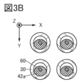
- 3A to 3E are schematic top views showing configuration examples of the semiconductor device.
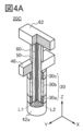
- 4A to 4C are cross-sectional perspective views showing configuration examples of transistors.
- 5A and 5D are top views showing configuration examples of the semiconductor device.
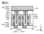
- 5B, 5C, and 5E are cross-sectional views showing configuration examples of the semiconductor device.
- 6A to 6C are cross-sectional views showing configuration examples of semiconductor devices.
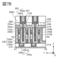
- 7A and 7B are cross-sectional views showing configuration examples of the semiconductor device.
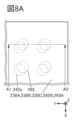
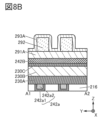
- 8A and 8C are top views showing an example of a method for manufacturing a semiconductor device.
- 8B and 8D are cross-sectional views illustrating an example of a method for manufacturing a semiconductor device.
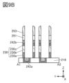
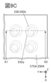
- 9A and 9C are top views showing an example of a method for manufacturing a semiconductor device.
- 9B and 9D are cross-sectional views illustrating an example of a method for manufacturing a semiconductor device.
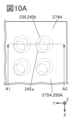
- 10A and 10C are top views illustrating an example of a method for manufacturing a semiconductor device.
- 10B and 10D are cross-sectional views illustrating an example of a method for manufacturing a semiconductor device.
- 11A and 11C are top views illustrating an example of a method for manufacturing a semiconductor device.
- FIG. 11B and 11D are cross-sectional views illustrating an example of a method for manufacturing a semiconductor device.
- FIG. 12A is a top view illustrating an example of a method for manufacturing a semiconductor device; 12B1 and 12B2 are cross-sectional views illustrating an example of a method for manufacturing a semiconductor device.
- 13A and 13C are top views illustrating an example of a method for manufacturing a semiconductor device.
- 13B and 13D are cross-sectional views illustrating an example of a method for manufacturing a semiconductor device.
- 14A and 14C are top views illustrating an example of a method for manufacturing a semiconductor device.
- 14B and 14D are cross-sectional views illustrating an example of a method for manufacturing a semiconductor device.
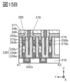
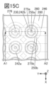
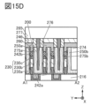
- 15A and 15C are top views illustrating an example of a method for manufacturing a semiconductor device.
- 15B and 15D are cross-sectional views illustrating an example of a method for manufacturing a semiconductor device.
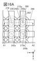
- FIG. 16A is a top view illustrating an example of a method for manufacturing a semiconductor device;
- 16B is a cross-sectional view illustrating an example of a method for manufacturing a semiconductor device;
- FIG. 17A is a cross-sectional view showing a configuration example of a storage device.
- 17B to 17D are cross-sectional views showing configuration examples of capacitive elements.
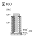
- 18A to 18E are cross-sectional views showing configuration examples of capacitive elements.
- FIG. 19A is a block diagram showing a configuration example of a storage device.
- FIG. 19B is a perspective view showing a configuration example of a storage device
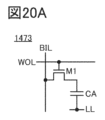
- FIG. FIG. 20A is a circuit diagram showing a configuration example of a memory cell.
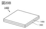
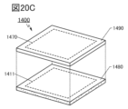
- 20B and 20C are perspective views showing configuration examples of the storage device.
- FIG. 21 is a cross-sectional view showing a configuration example of a storage device.
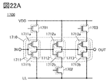
- FIG. 22A is a circuit diagram showing a configuration example of a semiconductor device.
- FIG. 22B is a perspective view showing a configuration example of a semiconductor device.
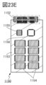
- 23A to 23E are diagrams for explaining an example of a storage device.
- 24A to 24G are diagrams for explaining an example of an electronic device.
- FIG. 25 is a cross-sectional view showing a configuration example of a storage device.
- top views also called “plan views”
- perspective views descriptions of some components may be omitted in order to facilitate understanding of the invention. Also, description of some hidden lines may be omitted.
- the ordinal numbers such as first and second are used for convenience and do not indicate the order of steps or the order of stacking. Therefore, for example, “first” can be appropriately replaced with “second” or “third”. Also, the ordinal numbers described in this specification and the like may not match the ordinal numbers used to specify one aspect of the present invention.
- connection relationships other than the connection relationships shown in the drawings or the text are not limited to the predetermined connection relationships, for example, the connection relationships shown in the drawings or the text.
- X and Y are objects (for example, devices, elements, circuits, wiring, electrodes, terminals, conductive films, layers, etc.).
- a transistor is an element having at least three terminals including a gate, a drain, and a source.
- a region in which a channel is formed (hereinafter also referred to as a channel formation region) is provided between the drain (drain terminal, drain region, or drain electrode) and the source (source terminal, source region, or source electrode).
- a current can flow between the source and the drain through the formation region.
- a channel formation region means a region where current mainly flows.
- the function of the source or drain may be switched when using transistors of different polarities or when the direction of current changes in circuit operation. Therefore, in this specification and the like, the terms “source” and “drain” may be used interchangeably.
- Impurities in a semiconductor refer to, for example, substances other than the main components that constitute the semiconductor.
- an element whose concentration is less than 0.1 atomic percent can be said to be an impurity.
- the inclusion of impurities may cause, for example, an increase in defect level density of a semiconductor, a decrease in crystallinity, and the like.
- impurities that change the characteristics of the semiconductor include, for example, group 1 elements, group 2 elements, group 13 elements, group 14 elements, group 15 elements, and oxide semiconductors.
- transition metals other than the main component such as hydrogen, lithium, sodium, silicon, boron, phosphorus, carbon, and nitrogen. Note that water may also function as an impurity.
- oxygen vacancies also referred to as V 2 O 3
- silicon oxynitride contains more oxygen than nitrogen as its composition.
- Silicon nitride oxide contains more nitrogen than oxygen in its composition.
- aluminum oxynitride has a higher content of oxygen than nitrogen as its composition.
- aluminum oxynitride has a composition in which the content of nitrogen is higher than that of oxygen.
- hafnium oxynitride has a higher content of oxygen than nitrogen as its composition.
- hafnium oxynitride has a composition in which the content of nitrogen is higher than that of oxygen.
- insulator can be replaced with an insulating film or an insulating layer.
- conductor can be replaced with a conductive film or a conductive layer.
- semiconductor can be interchanged with a semiconductor film or a semiconductor layer.
- parallel means a state in which two straight lines are arranged at an angle of -10 degrees or more and 10 degrees or less. Therefore, the case of ⁇ 5 degrees or more and 5 degrees or less is also included.
- substantially parallel means a state in which two straight lines are arranged at an angle of -30 degrees or more and 30 degrees or less.
- Perfect means that two straight lines are arranged at an angle of 80 degrees or more and 100 degrees or less. Therefore, the case of 85 degrees or more and 95 degrees or less is also included.
- substantially perpendicular means a state in which two straight lines are arranged at an angle of 60 degrees or more and 120 degrees or less.
- a metal oxide is a metal oxide in a broad sense.
- Metal oxides are classified into oxide insulators, oxide conductors (including transparent oxide conductors), oxide semiconductors (also referred to as oxide semiconductors or simply OSs), and the like.
- oxide semiconductors also referred to as oxide semiconductors or simply OSs
- an OS transistor can be referred to as a transistor including a metal oxide or an oxide semiconductor.
- the term “normally-off” means that the drain current per 1 ⁇ m of the channel width flowing through the transistor when no potential is applied to the gate or when a ground potential is applied to the gate is 1 ⁇ 10 ⁇ 1 at room temperature. 20 A or less, 1 ⁇ 10 ⁇ 18 A or less at 85° C., or 1 ⁇ 10 ⁇ 16 A or less at 125° C.
- Voltage is a potential difference from a reference potential.
- the reference potential is ground potential
- “voltage” can be replaced with “potential”. Note that the ground potential does not necessarily mean 0V.
- the potential is relative, and when the reference potential changes, the potential applied to the wiring, the potential applied to the circuit, etc., and the potential output from the circuit etc. also change.
- the heights are the same or approximately the same” refers to a configuration in which the heights from a reference surface (for example, a flat surface such as a substrate surface) are equal in cross-sectional view.
- planarization processing typically CMP processing
- CMP processing may expose the surface of a single layer or multiple layers.
- the surfaces to be planarized have the same height from the reference surface.
- the heights of the multiple layers may differ depending on the processing apparatus, processing method, or material of the surface to be processed in the planarization process. In this specification and the like, this case is also treated as "the height matches or roughly matches".
- the height of the top surface of the first layer and the height of the second layer When the difference in height from the upper surface of the layer is 20 nm or less, it is also said that the heights are the same or approximately the same.
- the ends match or roughly match means that at least part of the outline overlaps between the laminated layers when viewed from the top.
- the upper layer and the lower layer may be processed by the same mask pattern, or partially by the same mask pattern.
- the contours do not overlap, and the upper contour may be positioned inside the lower contour, or the upper contour may be positioned outside the lower contour. “match or approximate match”.
- FIG. 1A is a top view of a semiconductor device having a plurality of transistors 20.
- arrows indicating the X direction, Y direction, and Z direction may be attached in the drawings.
- "X direction” means a direction along the X axis, and there are cases where the forward direction and the reverse direction are not distinguished. The same applies to the "Y direction” and the "Z direction”.
- the X direction, the Y direction, and the Z direction are directions that cross each other. More specifically, the X-direction, Y-direction, and Z-direction are directions orthogonal to each other.
- first direction or “first direction”
- second direction or a “second direction”
- third direction or “third direction”.
- a semiconductor device of one embodiment of the present invention has a plurality of transistors 20 .
- FIG. 1A shows an example in which a semiconductor device has a plurality of transistors 20 arranged in a matrix of m rows and n columns (m and n are each independently an integer of 2 or more).
- rows and columns extend in directions orthogonal to each other.
- the X direction is defined as “row” and the Y direction is defined as “column”. Note that the X direction may be defined as “columns” and the Y direction may be defined as “rows.”
- the transistor 20 in row 1, column 1 is denoted by transistor 20[1,1]
- the transistor 20 in row m, column 1 is denoted by transistor 20[m,1]
- the transistor 20 in row 1 column n is denoted by transistor 20[m,1].
- transistor 20[1,n] the transistor 20 in the m-th row and n-th column is denoted as transistor 20[m,n].
- an arbitrary row may be indicated as i row.
- it may be described as j column. Therefore, i is an integer of 1 or more and m or less, and j is an integer of 1 or more and n or less.
- the transistor 20 in the i-th row and the j-th column is indicated as a transistor 20[i,j].
- i+ ⁇ ⁇ is a positive or negative integer
- i+ ⁇ does not fall below 1 and does not exceed m.
- j+ ⁇ when denoting "j+ ⁇ ", "j+ ⁇ " is not less than 1 and does not exceed n.
- the semiconductor device of one embodiment of the present invention includes m conductors 62 extending in the row direction and n conductors 46 extending in the column direction.
- the first (first row) conductor 62 is indicated as conductor 62[1]
- the m-th (m-th row) conductor 62 is indicated as conductor 62[m].
- the first (first column) conductor 46 is denoted as conductor 46[1]
- the nth (nth column) conductor 46 is denoted as conductor 46[n].
- the transistor 20[i,j] is located below the region where the i-th row conductor 62 (conductor 62[i]) and the j-th row conductor 46 (conductor 46[j]) intersect. Transistor 20[i,j] is also electrically connected to conductor 62[i] and conductor 46[j]. Transistor 20[i,j] also has an oxide 30[i,j] in which the channel is formed.
- the conductors 62 described hereinafter refer to any one or more of the conductors 62[1] to 62[m].
- the conductors 46 described hereinafter refer to any one or more of the conductors 46[1] to 46[n].
- the transistor 20 described hereinafter refers to one or more of the transistors 20[1,1] to 20[m,n].
- a conductor 46 is provided above the transistor 20 and a conductor 62 is provided above the conductor 46 .
- the conductors 62 and 46 are orthogonal because the conductors 62 extend in the row direction and the conductors 46 extend in the column direction.
- the conductors 62 and 46 function as wiring.
- FIG. 1B is a perspective view of transistor 20 including a cross section corresponding to the portion indicated by the dashed line L1-L2 in FIG. 1A. Note that in perspective views including cross sections such as FIG. 1B, a hatching pattern is applied only to the cross sections for the sake of clarity. A perspective view including a cross section as shown in FIG. 1B may be referred to as a cross-sectional perspective view.
- transistors 20[1,1] to 20[m,n] have the same configuration, they are denoted as the transistor 20 in FIG.
- the transistor 20 illustrated in FIG. 1B includes a conductor 42a, an oxide 30 over the conductor 42a, a conductor 42b over the oxide 30, an insulator 50, and a conductor 60.
- the conductor 42a, the oxide 30, and the conductor 42b have a circular shape when viewed from above. Also, the conductor 42a, the oxide 30, and the conductor 42b extend in the Z direction. Therefore, as shown in FIG. 1B, the conductor 42a, the oxide 30, and the conductor 42b have a cylindrical shape (also referred to as a columnar shape). Note that the cylindrical shape of the conductor 42a, the oxide 30, and the conductor 42b extends in the Z direction. Also, the conductor 42a has a recess.
- oxide 30 and the conductor 42b have openings in regions overlapping with the recesses of the conductor 42a when viewed from above. That is, as shown in FIG. 1A, the top surfaces of oxide 30 and conductor 42b have a hollow circular shape. In other words, oxide 30 and conductor 42b have a hollow cylindrical shape. Note that the openings of the oxide 30 and the conductor 42b are sometimes referred to as openings, hollows, hollows, and the like. A cylindrical shape provided with a hollow portion may be called a hollow cylindrical shape.
- the present invention is not limited to this.
- the top surface of the oxide 30 may have a hollow elliptical shape, a hollow polygonal shape, or a hollow polygonal shape with rounded corners.
- polygonal shapes refer to triangles, quadrilaterals, pentagons, hexagons, and the like.
- the conductor 42a when the conductor 42a has a recess and the oxide 30 and the conductor 42b have an opening, it is expressed as a laminate of the conductor 42a, the oxide 30, and the conductor 42b having a recess. There is Note that the conductor 42a may have an opening. At this time, the laminate of the conductor 42a, the oxide 30, and the conductor 42b may be described as having an opening.
- the insulator 50 and the conductor 60 are arranged inside the recess of the conductor 42a and inside the opening of the oxide 30 and the conductor 42b.
- the insulator 50 has a region in contact with the side surface of the conductor 60 and a region in contact with the bottom surface of the conductor 60 .
- the conductor 60 functions as a gate electrode.
- Insulator 50 also functions as a gate insulator.
- the gate insulator is sometimes called a gate insulating layer or a gate insulating film.
- the conductor 42a functions as one of the source electrode and the drain electrode, and the conductor 42b functions as the other of the source electrode and the drain electrode.
- At least part of the region of the oxide 30 overlapping with the conductor 60 functions as a channel formation region. Note that the region of the oxide 30 overlapping with the conductor 60 can be rephrased as a region of the oxide 30 facing the conductor 60 with the insulator 50 interposed therebetween.
- the transistor 20 is a so-called vertical transistor in which one of the source electrode and the drain electrode is positioned below the channel formation region and the other of the source electrode and the drain electrode is positioned above the channel formation region so that current flows vertically. is.
- Vertical transistors can be formed at crosspoints where minimum-pitch wiring intersects. Specifically, transistor 20 is formed below the region where conductor 62 and conductor 46 intersect. Therefore, miniaturization or high integration of the semiconductor device can be achieved. Specifically, it becomes possible to minimize the design rule from 6F2 to 4F2 .
- the channel length of the transistor 20 is the region where the semiconductor (or the portion of the semiconductor in which current flows when the transistor is on) overlaps with the gate electrode in a cross-sectional view, or the source in the channel formation region. region or source electrode) and the drain (drain region or drain electrode). That is, the channel length of transistor 20 corresponds to the thickness of oxide 30 . Therefore, since the channel length of the transistor 20 can be adjusted by changing the thickness of the oxide 30, the transistor 20 with a short channel length can be manufactured by reducing the thickness of the oxide 30.
- the channel length of the transistor 20 is, for example, 30 nm or less, 20 nm or less, 15 nm or less, 10 nm or less, 8 nm or less, or 5 nm or less. be able to. That is, it is preferable to form the oxide 30 so that the film thickness is, for example, 3 nm or more and 30 nm or less. Since the OS transistor has extremely low off-state current, the off-state current of the transistor 20 can be reduced even with the above channel length.
- the channel length of the transistor may be lengthened in order to improve electrical characteristics in the saturation region. Since the transistor 20 is a vertical transistor, the area occupied by the transistor 20 in top view does not depend on the film thickness of the oxide 30 . Therefore, the film thickness of the oxide 30 corresponding to the channel length may be thick. For example, the thickness of the oxide 30 may be greater than 30 nm and less than or equal to 100 nm.
- the film thickness of the oxide 30 is set to 3 nm or more and 100 nm or less, preferably 3 nm or more and 30 nm or less, more preferably 5 nm or more and 30 nm or less, further preferably 5 nm or more and 15 nm or less.
- the channel width of the transistor 20 is the region in which the semiconductor (or the portion of the semiconductor in which current flows when the transistor is on) and the gate electrode overlap each other, or the channel length direction in the channel formation region when viewed from the top.
- the channel width does not always have the same value in all regions of one transistor. That is, the channel width of one transistor may not be fixed to one value. Therefore, in this specification, the channel width is any one value, maximum value, minimum value, or average value in the channel forming region.
- the values of the channel length and channel width can be determined by, for example, analyzing a cross-sectional TEM image.
- the transistor 20 preferably uses a metal oxide functioning as a semiconductor (hereinafter also referred to as an oxide semiconductor) for the oxide 30 including the channel formation region.
- a metal oxide functioning as a semiconductor hereinafter also referred to as an oxide semiconductor
- the bandgap of the metal oxide that functions as a semiconductor is preferably 2 eV or more, more preferably 2.5 eV or more.
- the off-state current of the transistor can be reduced by using a metal oxide with a large bandgap.
- the oxide 30 preferably contains at least indium or zinc. In particular, it preferably contains indium and zinc. In addition, it preferably contains one or more selected from aluminum, gallium, yttrium, and tin. It may also contain one or more selected from boron, silicon, titanium, iron, nickel, germanium, zirconium, molybdenum, lanthanum, cerium, neodymium, hafnium, tantalum, tungsten, magnesium, cobalt, and the like. .
- the element M is aluminum, gallium, yttrium, or tin.
- Other applicable elements for element M include boron, silicon, titanium, iron, nickel, germanium, zirconium, molybdenum, lanthanum, cerium, neodymium, hafnium, tantalum, tungsten, magnesium, or cobalt.
- the element M there are cases where a plurality of the above elements may be combined.
- the element M is preferably one or more selected from gallium, aluminum, yttrium, and tin.
- an In--Ga oxide, an In--Zn oxide, or an indium oxide may be used as the oxide 30.
- the neighboring composition includes a range of ⁇ 30% of the desired atomic number ratio.
- an oxide also referred to as IGZO
- IGZO oxide containing indium (In), gallium (Ga), and zinc (Zn)
- an oxide containing indium (In), aluminum (Al), and zinc (Zn) also referred to as IAZO
- IAGZO oxide containing indium (In), aluminum (Al), gallium (Ga), and zinc (Zn)
- nitrogen-containing metal oxides may also be collectively referred to as metal oxides.
- a metal oxide containing nitrogen may also be referred to as a metal oxynitride.
- the electrical characteristics of the vertical transistor become unstable due to the substrate floating effect.
- metal oxides such as IGZO, IAZO, and IAGZO have large hole effective masses. Therefore, by using the metal oxide for the channel formation region, it is possible to suppress the accumulation of holes in the channel formation region and manufacture a vertical transistor with little or substantially no substrate floating effect. can. That is, by using the above metal oxide for the oxide 30, the transistor 20 can have stable electrical characteristics. Therefore, a transistor with favorable electrical characteristics can be provided. Further, a transistor with little variation in electrical characteristics can be provided.
- the oxide 30 preferably has crystallinity.
- CAAC-OS c-axis aligned crystal oxide semiconductor
- CAAC-OS is a metal oxide that has a dense structure with high crystallinity and few impurities and defects (such as oxygen vacancies).
- heat treatment is performed at a temperature at which the metal oxide does not become polycrystalline (for example, 400° C. or higher and 600° C. or lower), so that the CAAC-OS has a dense structure with higher crystallinity.
- a temperature at which the metal oxide does not become polycrystalline for example, 400° C. or higher and 600° C. or lower
- the oxide 30 by using a crystalline metal oxide such as CAAC-OS as the oxide 30, extraction of oxygen from the oxide 30 by the source electrode or the drain electrode can be suppressed. As a result, the extraction of oxygen from the oxide 30 can be reduced even if heat treatment is performed, so the transistor 20 is stable against high temperatures (so-called thermal budget) in the manufacturing process.
- a crystalline metal oxide such as CAAC-OS
- the c-axis of the crystal of the CAAC-OS is oriented in a direction perpendicular or substantially perpendicular to the formation surface or upper surface of the metal oxide film to be the oxide 30.
- the crystals of CAAC-OS are c-axis oriented with respect to the formation surface or top surface of the metal oxide film to be the oxide 30 . That is, the crystals of the oxide 30 are c-axis oriented with respect to the substrate surface.
- the crystal structure of the oxide 30 may be, for example, a YbFe2O4 type structure or a Yb2Fe3O7 structure . type structures, and variations of these structures.
- the film formation of the oxide 30 is performed by a sputtering method, a chemical vapor deposition (CVD) method, a molecular beam epitaxy (MBE) method, a pulsed laser deposition (PLD) method, or an atomic It can be carried out using a layer deposition (ALD: Atomic Layer Deposition) method or the like.
- the film formation of the oxide 30 is preferably performed using a sputtering method.
- a sputtering method By using a sputtering method, a crystalline metal oxide can be formed.
- the sputtering method is a film formation method capable of forming a thin film, it can be suitably used for film formation of the oxide 30 .
- a recess or an opening is formed in the stack of the conductor 42a, the oxide 30, and the conductor 42b, and the insulator 50 and the conductor 60 are formed inside the recess or the opening. produced.
- the oxide 30 may be formed on the conductor 42a, and high step coverage is not required when the oxide 30 is formed. Therefore, the film formation method of the oxide 30 can be freely applied. For example, a sputtering method can be used to form the oxide 30, and a crystalline metal oxide can be formed.
- the formation of the recess or the opening includes double patterning such as LELE (Litho-Etch-Litho-Etch) and SADP (Self-Aligned Double Patterning), quadruple patterning such as SAQP (Self-Aligned Quadruple Patterning),
- multi-patterning techniques such as octal patterning may be used. By using the multi-patterning technique, fine recesses or fine openings can be formed.
- the opening of the resist pattern may be reduced by using a shrink agent for the resist pattern.
- a shrink agent for the resist pattern.
- heat treatment is performed.
- the resist reacts with the shrink agent to form a reaction layer on the surface of the resist.
- the opening can be reduced.
- the shrink agent is sometimes called a pattern shrink agent or a hole shrink agent.
- a fine pattern may be directly formed by exposure using EUV (Extreme Ultraviolet) light or the like.
- patterning may be performed by combining the above methods.
- a cylindrical channel having a hollow portion is formed using a multi-patterning technique such as SAQP.
- a multi-patterning technique such as SAQP.
- a vertical transistor structure in which the gate electrode is provided in the hollow portion a transistor that can be miniaturized can be provided.
- a memory cell with a minimum feature size (F) of, for example, 15 nm or less can be realized.
- the minimum processing dimension (F) is, for example, the width of the conductor 46 in the X direction or the width of the conductor 62 in the Y direction.
- the conductor 42 a is provided in contact with the bottom surface of the oxide 30
- the conductor 42 b is provided in contact with the top surface of the oxide 30 .
- the conductor 42a and the conductor 42b may be collectively referred to as the conductor 42 below.
- a nitride containing tantalum for example, a nitride containing tantalum, a nitride containing titanium, a nitride containing molybdenum, a nitride containing tungsten, a nitride containing tantalum and aluminum, a nitride containing titanium and aluminum, or the like is used. It is preferable to use In one aspect of the present invention, nitrides containing tantalum are particularly preferred. Alternatively, for example, ruthenium oxide, ruthenium nitride, an oxide containing strontium and ruthenium, an oxide containing lanthanum and nickel, or the like may be used. These materials are preferable because they are conductive materials that are difficult to oxidize or materials that maintain conductivity even after absorbing oxygen.
- the conductive film to be the conductor 42a and the conductive film to be the conductor 42b are formed in different steps. Therefore, the conductors 42a and 42b may be made of different materials or may be made of the same material.
- hydrogen contained in the oxide 30 and the like may diffuse into the conductor 42a.
- hydrogen contained in the oxide 30 or the like easily diffuses into the conductor 42a, and the diffused hydrogen can be bonded to nitrogen included in the conductor 42a. be. That is, hydrogen contained in the oxide 30 or the like may be absorbed by the conductor 42a.
- hydrogen contained in the oxide 30 or the like may diffuse into the conductor 42b.
- hydrogen contained in the oxide 30 or the like easily diffuses into the conductor 42b, and the diffused hydrogen can be bonded to nitrogen included in the conductor 42b. be. In other words, hydrogen contained in the oxide 30 or the like may be absorbed by the conductor 42b.
- the sheet resistance of the oxide 30 near the conductor 42a may decrease.
- the carrier concentration may increase. Therefore, the resistance of the oxide 30 in the vicinity of the conductor 42a can be reduced in a self-aligning manner.
- the sheet resistance of the oxide 30 near the conductor 42b may decrease.
- the carrier concentration may increase. Therefore, the resistance of the oxide 30 in the vicinity of the conductor 42b can be reduced in a self-aligned manner.
- FIG. 1C is a cross-sectional perspective view of the transistor 20.
- a region 30n1 is a low-resistance region of the oxide 30 near the conductor 42a
- a region 30n2 is a low-resistance region of the oxide 30 near the conductor 42b.
- Region 30n1 and region 30n2 function as a source region or a drain region.
- a region of oxide 30 that functions as a channel forming region is denoted as region 30i. Note that it may be difficult to clearly detect boundaries between regions in the oxide 30 .
- region 30n1 may not be formed depending on the material used for the conductor 42a.
- the oxide 30 now has a region 30i and a region 30n2.
- region 30n2 may not be formed.
- the oxide 30 has a region 30n1 and a region 30i.
- the insulator 50 is preferably formed using an insulator having a function of suppressing diffusion of oxygen.
- diffusion of oxygen contained in the oxide 30 to the conductor 60 can be suppressed. That is, the formation of oxygen vacancies in the oxide 30 can be suppressed.
- oxidation of the conductor 60 by oxygen contained in the oxide 30 can be suppressed. Therefore, the electrical characteristics of the transistor 20 can be improved, and the reliability can be improved.
- the insulator 50 it is preferable to use an insulator containing oxides of one or both of aluminum and hafnium, for example.
- an insulator aluminum oxide, hafnium oxide, an oxide containing aluminum and hafnium (hafnium aluminate), an oxide containing hafnium and silicon (hafnium silicate), or the like can be used.
- the insulator 50 may use a high dielectric constant (high-k) material.
- high-k high dielectric constant
- EOT equivalent oxide thickness
- High dielectric constant materials include gallium oxide, hafnium oxide, zirconium oxide, oxides with aluminum and hafnium, oxynitrides with aluminum and hafnium, oxides with silicon and hafnium, oxynitrides with silicon and hafnium, Or there are nitrides with silicon and hafnium.
- the insulator 50 extends in the Z direction so that the upper surface of the insulator 50 is positioned above the conductor 42b. This prevents the conductor 42b and the conductor 62 from coming into contact with each other, thereby preventing leakage current and short circuit between the conductor 42b and the conductor 62. FIG. Similarly, contact between the conductors 46 and 62 can be prevented to prevent leakage currents and short circuits between the conductors 46 and 62 .
- FIG. 1B shows a structure in which the insulator 50 is a single layer
- the present invention is not limited to this, and a laminated structure of two or more layers may be used.
- the insulator 50 has a two-layer structure
- the insulator provided on the oxide 30 side is formed using an insulator having a function of suppressing diffusion of oxygen, and the insulator provided on the conductor 60 side is used.
- the conductor 60 preferably uses a conductive material that has a function of suppressing the diffusion of impurities such as hydrogen atoms, hydrogen molecules, water molecules, nitrogen atoms, nitrogen molecules, nitrogen oxide molecules, and copper atoms.
- a conductive material having a function of suppressing diffusion of oxygen eg, at least one of oxygen atoms and oxygen molecules is preferably used.
- the conductor 60 has a function of suppressing the diffusion of oxygen, it is possible to suppress the oxidation of the conductor 60 due to the oxygen contained in the insulator 50 and the decrease in conductivity.
- the conductive material having a function of suppressing diffusion of oxygen titanium, titanium nitride, tantalum, tantalum nitride, ruthenium, ruthenium oxide, or the like is preferably used, for example.
- the conductor 46 has a region in contact with the conductor 42 b, and the conductor 62 has a region in contact with the conductor 60 .
- the conductors 46 and 62 function as wiring.
- the conductor 46 has an opening. Also, an insulator 50 and a conductor 60 are provided in the opening.
- the conductor 46 extends in the Y direction as a continuous conductor.
- the conductor 46 is divided by the insulator 50. .
- the separated conductors 46 are electrically connected via the conductor 42b. Therefore, since the conductor 46 extends in the Y direction via the conductor 42b, it can be regarded as extending in the Y direction.
- the conductor 46 may or may not have a region overlapping the conductor 62 .
- the conductors 46 and 62 preferably use a conductive material containing tungsten, copper, or aluminum as a main component. Also, one or both of the conductor 46 and the conductor 62 may have a laminated structure, for example, a laminated structure of titanium or titanium nitride and the above conductive material.
- FIG. 1B shows a configuration in which the oxide 30 is a single layer
- the present invention is not limited to this.
- the oxide 30 may have a laminated structure of two or more layers.
- FIG. 2A is a cross-sectional perspective view of transistor 20A.
- Transistor 20A shown in FIG. 2A is a variation of transistor 20 shown in FIG. 1B.
- the transistor 20A shown in FIG. 2A differs from the transistor 20 shown in FIG. 1B in that the oxide 30 has a three-layer structure of oxides 30a, 30b, and 30c.
- Oxide 30b functions as a channel forming region of transistor 20A
- oxide 30a functions as one of the source and drain regions of transistor 20A
- oxide 30c functions as the other of the source and drain regions of transistor 20A. Function.
- a metal oxide that can be used for the oxide 30 described above may be used as the oxide 30b.
- the oxides 30a and 30c are preferably made of materials with higher electrical conductivity than the oxide 30b.
- a degenerate oxide semiconductor is preferably used for the oxides 30a and 30c.
- the oxide 30a and the oxide 30c a material obtained by adding nitrogen to the metal oxide that can be used for the oxide 30b can be used.
- a metal oxide also referred to as a metal oxynitride
- indium, the above element M, zinc, and nitrogen is preferably used.
- an oxide containing indium (In), gallium (Ga), zinc (Zn), and nitrogen also referred to as an oxynitride containing In, Ga, and Zn, or IGZO to which nitrogen is added
- oxides containing indium (In), aluminum (Al), zinc (Zn), and nitrogen also called oxynitrides containing In, Al, and Zn, or nitrogen-added IAZO
- indium ( In) aluminum (Al), gallium (Ga), zinc (Zn)
- oxides containing nitrogen oxygen (oxynitrides with In, Al, Ga, and Zn, nitrogen-added IAGZO, nitrogen-added (also referred to as IGAZO or nitrogen-added AGIZO) can be used.
- nitrogen-doped IGZO tends to have a wurtzite crystal structure.
- the wurtzite crystal structure has high lattice matching with the crystal structure of the In-M-Zn oxide. Therefore, by using a metal oxynitride having a wurtzite crystal structure as the oxide 30a, the crystallinity of the oxide 30b can be improved. That is, it becomes easy to form a metal oxide having a CAAC structure as the oxide 30b.
- CAAC-OS when CAAC-OS is used as the oxide 30b, crystals of the oxide 30b are c-axis oriented with respect to the substrate surface. Note that impurities in the CAAC-OS tend to be difficult to diffuse in the c-axis direction. That is, by using CAAC-OS as the oxide 30b, entry of impurities into the oxide 30b can be suppressed. For example, nitrogen can be suppressed from entering the oxide 30b. Therefore, it is possible to suppress an increase in the conductivity of the oxide 30b.
- any element that enhances the Examples of such elements include hydrogen, group 15 elements (typically nitrogen (N), phosphorus (P), arsenic (As), and antimony (Sb)), boron (B), aluminum (Al), argon ( Ar), helium (He), neon (Ne), indium (In), fluorine (F), chlorine (Cl), titanium (Ti), and zinc (Zn).
- group 15 elements typically nitrogen (N), phosphorus (P), arsenic (As), and antimony (Sb)
- Al aluminum
- Ar argon
- He helium
- neon Ne
- In indium
- F fluorine
- F chlorine
- Ti titanium
- Zn zinc
- the metal oxides used for the oxides 30a and 30c should have higher conductivity than the oxide 30b.
- the oxide 30a and the oxide 30c may be metal oxides having a common element other than oxygen as the main component of the oxide 30b and having different chemical compositions.
- the oxide 30 preferably has a laminated structure of multiple oxide layers with different chemical compositions.
- the atomic ratio of indium to the metal element which is the main component in the metal oxide used for the oxide 30a or the oxide 30c is equal to that of the metal used for the oxide 30b. It is preferably larger than the atomic ratio of indium to the metal element which is the main component in the oxide.
- the atomic ratio of indium to the element M in the metal oxide used for the oxide 30a or the oxide 30c is higher than the atomic ratio of indium to the element M in the metal oxide used for the oxide 30b.
- the defect level density at the interface between the oxide 30a or the oxide 30c and the oxide 30b can be reduced. can do. Since the defect level density at the interface between the oxide 30a or the oxide 30c and the oxide 30b can be reduced, the effect of interface scattering on carrier conduction is small, and a high on-current can be obtained.
- oxide 30a and oxide 30c titanium oxide, molybdenum oxide, zinc oxide, indium oxide, tungsten oxide, magnesium oxide, calcium oxide, tin oxide, indium zinc oxide, indium tin oxide, or indium containing silicon Tin oxide or the like may also be used.
- FIG. 2A shows a configuration in which the contour of the conductor 42a matches or roughly matches the outer contour of the oxide 30 when viewed from above
- the present invention is not limited to this.
- the contour of the conductor 42a does not have to match the outer contour of the oxide 30 when viewed from above.
- FIG. 2B is a cross-sectional perspective view of transistor 20B.
- the transistor 20B shown in FIG. 2B is a modification of the transistor 20A shown in FIG. 2A.
- the transistor 20B shown in FIG. 2B differs from the transistor 20A shown in FIG. 2A in that the center of the conductor 42a does not coincide with the center of the hollow cylindrical shape of the oxide 30 when viewed from above.
- the diameter of the conductor 42a and the diameter of the hollow portion of the oxide 30 In order to miniaturize the semiconductor device, it is necessary to reduce the diameter of the conductor 42a and the diameter of the hollow portion of the oxide 30 when viewed from above.
- the diameter of the conductor 42a and the diameter of the hollow portion of the oxide 30 match or approximately match.
- the conductor 42a and the oxide 30 may not overlap each other, and the conductor 42a and the oxide 30 may not contact each other.
- the conductor 42a is arranged at a position offset from the center of the hollow cylindrical shape of the oxide 30 and the conductor 42b when viewed from above, and the oxide 30 and the conductor 42b It is preferable to have a region overlapping with .
- the conductor 42a can have a region in contact with the oxide 30a.
- the conductor 42a, the oxide 30 and the conductor 42b can be formed independently. Therefore, the degree of freedom in layout of the semiconductor device can be increased.
- 3A-3E are top views of transistor 20B.
- the conductor 60, the oxide 30, and the conductor 42a are illustrated and some elements are omitted for clarity of illustration.
- the conductor 42a may have a region that overlaps with the oxide 30, and may be arranged at a position shifted in the X direction from the center of the hollow cylindrical shape of the oxide 30. Also, the outline of the conductor 42 a is located inside the outer circumference of the hollow cylindrical shape of the oxide 30 .
- the conductor 42a may have a region that overlaps with the oxide 30 and may be arranged at a position shifted in the Y direction from the center of the hollow cylindrical shape of the oxide 30. . Also, the outline of the conductor 42 a is located inside the outer circumference of the hollow cylindrical shape of the oxide 30 .
- a part of the outline of the conductor 42a is larger than the outer periphery of the hollow cylindrical shape of the oxide 30. May be located outside.
- the conductor 42a has a region that overlaps with the oxide 30, and is arranged at a position shifted in the X direction and the Y direction from the center of the hollow cylindrical shape of the oxide 30. may Note that, as shown in FIG. 3C, a portion of the outline of the conductor 42a may be located outside the outer periphery of the hollow cylindrical shape of the oxide 30.
- the upper surface of the oxide 30 has a hollow circular shape, but the present invention is not limited to this.
- the top surface of the oxide 30 may have a hollow elliptical shape, a hollow polygonal shape, or a hollow polygonal shape with rounded corners.
- the top surface of oxide 30 has a hollow square shape with rounded corners
- the top surface of conductor 42a and conductor 60 has a square shape with rounded corners.
- the conductor 42a has a region that overlaps with the oxide 30, and is arranged at a position shifted from the center of the hollow cylindrical shape of the oxide 30 in the X and Y directions. 3D, a part of the outline of the conductor 42a may be located outside the outer circumference of the hollow cylindrical shape of the oxide 30. As shown in FIG.
- 3A to 3D show a configuration in which the diameter of the conductor 42a and the diameter of the hollow portion of the oxide 30 are the same. A similar configuration can also be used when the distance is small.
- the conductor 42a and the oxide 30 can be formed independently; therefore, the top surface shape of the conductor 42a and the top surface shape of the hollow portion of the oxide 30 may be different.
- the top surface of the oxide 30 may have a hollow circular shape
- the top surface of the conductor 42a may have a polygonal shape (sometimes referred to as a substantially polygonal shape) with rounded corners.
- the center of the conductor 42a is aligned with the center of the hollow cylinder of the oxide 30. good too.
- the conductor 42a has a region that overlaps with the oxide 30, and the outline of the conductor 42a is located inside the outer periphery of the hollow cylindrical shape of the oxide 30.
- the outline of the conductor 42a may be located inside the outer circumference of the hollow cylindrical shape of the oxide 30. may be arranged at positions shifted to one or both of
- Transistor 20C A configuration example different from the transistor 20A described above is shown in FIG. 4A.
- FIG. 4A is a cross-sectional perspective view of transistor 20C.
- Transistor 20C shown in FIG. 4A is a modification of transistor 20A shown in FIG. 2A.
- the transistor 20C shown in FIG. 4A differs from the transistor 20A shown in FIG. 2A in that it does not have a conductor 42b.
- the conductor 46 also has the function of the conductor 42b. That is, the conductor 46 has a function as a wiring and a function as the other of the source electrode and the drain electrode.
- Transistor 20D A configuration example different from the transistor 20A described above is shown in FIG. 4B.
- FIG. 4B is a cross-sectional perspective view of transistor 20D.
- Transistor 20D shown in FIG. 4B is a modification of transistor 20A shown in FIG. 2A.
- a transistor 20D shown in FIG. 4B has a different shape of the conductor 46 from the transistor 20A shown in FIG. 2A.
- a region 64a shown in FIG. 4B is a region where the conductor 46 and the conductor 42b overlap when viewed from above. Note that the region 64 a does not overlap the conductor 62 .
- a region 64b shown in FIG. 4B is a region where the conductor 46, the conductor 42b, and the conductor 62 overlap each other when viewed from above.
- the conductor 46 has a convex shaped portion 46a in a region overlapping the regions 64a and 64b.
- the conductor 46 is in contact with the conductor 42b at the convex shaped portion 46a.
- the convex shaped portion 46a is formed when the conductor 46 is formed on an insulator (not shown in FIG. 4B) having an opening in a region overlapping the conductor 42b. A method of forming the conductor 46 having the convex shaped portion will be described in the second embodiment.
- FIG. 4B shows a configuration in which the conductor 46 has the convex shape portion 46a in the region overlapping the regions 64a and 64b
- the present invention is not limited to this, and the convex shape portion 46a is It may be in contact with at least part of the upper surface of the conductor 42b.
- FIG. 4C is a cross-sectional perspective view of transistor 20E.
- Transistor 20E shown in FIG. 4C is a modification of transistor 20D shown in FIG. 4B.
- the transistor 20E shown in FIG. 4C has a different shape of the conductor 46 from the transistor 20D shown in FIG. 4B.
- the conductor 46 of the transistor 20E does not overlap the conductor 62 when viewed from above.
- the conductor 46 has a convex shaped portion 46a in a region overlapping with the region 64a.
- the convex shaped portion 46a does not overlap the region 64b shown in FIG. 4B.
- the conductor 46 may have a region in contact with the insulator 50 or may not be in contact with the insulator 50. .
- the distance between the conductor 62 and the conductor 46 can be increased. Therefore, leakage current and short circuit between the conductor 62 and the conductor 46 can be prevented. Note that if leakage current and short-circuiting between the conductor 62 and the conductor 46 can be prevented, the conductor 62 and the conductor 46 have overlapping regions as shown in FIGS. You may
- a semiconductor device that can be miniaturized or highly integrated can be provided.
- a highly reliable semiconductor device can be provided.
- a semiconductor device with favorable electrical characteristics can be provided.
- a semiconductor device with large on-current can be provided.
- a semiconductor device of one embodiment of the present invention includes a plurality of transistors.
- FIGS. 5A to 5E are a top view and cross-sectional views of a semiconductor device of one embodiment of the present invention.
- 5A and 5D are top views of the semiconductor device.
- 5B, 5C, and 5E are cross-sectional views of the semiconductor device.
- FIG. 5B is a cross-sectional view of the portion indicated by the dashed-dotted line A1-A2 in FIG. 5A.
- FIG. 5C is sectional drawing of the site
- FIG. 5D is a top view of the area surrounded by the two-dot chain line in FIG. 5A including the cross section of the portion indicated by the one-dot chain line C1-C2 in FIG. 5B.
- FIG. 5E is a cross-sectional view of the portion indicated by the dashed-dotted line B3-B4 in FIG. 5A. Note that some elements are omitted from the top views of FIGS. 5
- FIGS. 5A to 5E includes a plurality of transistors 200.
- FIG. FIG. 5A shows an example in which a semiconductor device has a plurality of transistors 200 arranged in a matrix. It should be noted that four transistors 200 are illustrated in the area surrounded by the two-dot chain line in FIG. 5A.
- the semiconductor device shown in FIGS. 5A-5E includes insulator 216 on a substrate (not shown), transistor 200, insulator 275b, insulator 250b, and insulator 274 on substrate and insulator 216, and transistor 200, insulator 275b, insulator 250b, and insulator 274, and insulator 277 and insulator 278 over insulator 277 and insulator 278;
- the insulator 216, the insulator 274, the insulator 277, the insulator 278, and the insulator 285 function as interlayer films.
- the semiconductor device also includes a conductor 246 and a conductor 262 .
- a conductor 246 that is electrically connected to the transistor 200 and functions as a wiring is provided over the transistor 200, the insulator 275b, the insulator 250b, and the insulator 274.
- a conductor 262 (a conductor 262 a and a conductor 262 b ) which is electrically connected to the transistor 200 and functions as a wiring is provided over the insulator 276 , the insulator 278 , and the transistor 200 .
- the conductor 262 extends in the X direction. Also, the conductor 246 extends in the Y direction. Therefore, it can be said that the direction in which the conductor 262 extends is perpendicular to the direction in which the conductor 246 extends.
- the conductor 246 and the conductor 262 do not overlap.
- the transistor 200 is located below the region where the conductor 262 and the region between the conductors 246 adjacent in the Y direction intersect.
- transistor 200 corresponds to the transistor 20 described in Embodiment 1 or its modification. Therefore, for the structure of the transistor 200, the contents of the transistor 20 and its modification described in Embodiment 1 can be taken into consideration. Note that FIGS. 5B to 5E illustrate the transistor 200 to which the configuration of the transistor 20E is applied.
- the transistor 200 includes a conductor 242a (a conductor 242a1 and a conductor 242a2) embedded in the insulator 216 and an oxide layer on the insulator 216 and the conductor 242a.
- a conductor 242a a conductor 242a1 and a conductor 242a2
- the transistor 200 includes a conductor 242a (a conductor 242a1 and a conductor 242a2) embedded in the insulator 216 and an oxide layer on the insulator 216 and the conductor 242a.
- the oxide 230a, the oxide 230b, and the oxide 230c may be collectively referred to as the oxide 230.
- the oxide 230 and conductor 242b have a cylindrical shape extending in the Z direction and have openings. That is, the oxide 230 and the conductor 242b have a cylindrical shape with a hollow portion (also referred to as a hollow cylindrical shape). In other words, the top surfaces of oxide 230 and conductor 242b have a hollow circular shape. In addition, the opening of the oxide 230 and the opening of the conductor 242b overlap.
- the insulator 275a, the insulator 250a, and the conductor 260 are arranged inside openings provided in the oxide 230 and the conductor 242b.
- the insulator 250 a has a region in contact with the side surface of the conductor 260 and a region in contact with the bottom surface of the conductor 260 .
- the insulator 275a has a region in contact with the side surface of the insulator 250a, a region in contact with the bottom surface of the insulator 250a, a region in contact with the side surface of the opening of the oxide 230, and a region in contact with the side surface of the opening of the conductor 242b. have. In such a configuration, insulator 275a and insulator 250a can be said to each have a recess.
- FIG. 5D corresponds to the XY plane at or near the center of the oxide 230b.
- the insulator 250a is provided concentrically outside the conductor 260, and the insulator 275a is provided concentrically outside the insulator 250a.
- the material 230b is provided concentrically outside the insulator 275a, and the insulator 275b is provided concentrically outside the oxide 230b.
- the width of the oxide 230b in the direction from the center of the hollow portion of the oxide 230b toward the outer periphery of the cylindrical shape is defined as the width H1.
- the width H1 is half the difference between the outer diameter and the inner diameter of the hollow cylindrical shape.
- the width H1 must be smaller than half the minimum feature size (F) so that the adjacent oxides 230b do not touch each other.
- the width H1 is preferably 1 nm or more and 7 nm or less, more preferably 1.5 nm or more and 6 nm or less, and more preferably 2 nm or more and 5 nm or less.
- the adjacent oxides 230b are not in contact with each other, and at least the insulator 275b can be provided between the adjacent oxides 230b.
- the preferable range of the width H1 is not limited to the above.
- the width H1 may be appropriately set in consideration of the minimum processing dimension, the film thickness of the insulator 275b, and the like.
- the present invention is not limited to this.
- the top surfaces of the oxide 230 and the conductor 242b may have a hollow elliptical shape, a hollow polygonal shape, or a hollow polygonal shape with rounded corners. good too.
- the oxide 230 has a region that overlaps with the conductor 242a. More specifically, oxide 230a has a region that contacts the top surface of conductor 242a. In addition, the oxide 230 overlaps with the conductor 242b. More specifically, oxide 230c contacts the bottom surface of conductor 242b. In addition, the conductor 242 b has a region in contact with the conductor 246 . Also, the conductor 260 has a region in contact with the conductor 262 .
- the top of the insulator 250a matches or substantially matches the top of the insulator 275a, the top of the insulator 275b, and the top of the insulator 250b.
- An insulator 276 is provided on the insulator 275a and the insulator 250a.
- a conductor 262 is located on the insulator 276 . That is, the insulator 276 is provided between the insulator 275 a and the insulator 250 a and the conductor 262 .
- the insulator 276 has regions that overlap with the insulators 275a and 250a. Insulator 276 also has a region in contact with the lower surface of conductor 262 . In other words, at least part of the lower surface of conductor 262 is in contact with the upper surface of insulator 276 .
- the insulator 276 functions as an interlayer film.
- the insulator 276 has a cylindrical shape and has an opening. That is, insulator 276 has a cylindrical shape with a hollow portion. In other words, the upper surface of insulator 276 has a hollow circular shape.
- a conductor 260 is provided in a hollow portion of the insulator 276 . Further, when the conductor 260 has a circular cross-sectional shape, the insulator 276 is provided concentrically outside the conductor 260 .
- the outer periphery of the hollow portion of the insulator 276 is preferably the same as or larger than the outer periphery of the region of the conductor 260 overlapping the oxide 230b. With such a configuration, the conductor 260 can be more reliably embedded in the recess of the insulator 250a.
- the cylindrical contour of the insulator 276 preferably matches or roughly matches the contour of the insulator 275a.
- the contact area between the conductors 242b and 246 can be increased compared to a structure in which the cylindrical contour of the insulator 276 is larger than the contour of the insulator 275a.
- the distance between the conductor 262 and the conductor 246 can be increased compared to a structure in which the cylindrical contour of the insulator 276 is smaller than the contour of the insulator 275a. can. Therefore, leakage current and short circuit between the conductor 262 and the conductor 246 can be prevented.
- the insulator 276 preferably extends in the Z direction so that the upper surface of the conductor 246 is positioned between the lower and upper surfaces of the insulator 276 .
- the insulator 276 extends in the Z direction so that the top surface of the conductor 246 is positioned above the bottom surface of the insulator 276 and below the top surface of the insulator 276. preferably.
- An insulator 277 is provided on the conductor 246 . As shown in FIG. 5E, insulator 277 and conductor 246 are coincident or nearly coincident at the ends.
- the conductor 260 functions as a gate electrode.
- the insulator 275a and the insulator 250a function as gate insulators.
- the conductor 242a functions as one of the source and drain electrodes
- the conductor 242b functions as the other of the source and drain electrodes.
- At least part of the region of the oxide 230 overlapping with the conductor 260 functions as a channel formation region.
- a region of the oxide 230 overlapping with the conductor 260 can be referred to as a region of the oxide 230 facing the conductor 260 with the insulator 275a and the insulator 250a interposed therebetween.
- oxide 230b functions as a channel-forming region
- oxide 230a functions as one of the source and drain regions
- oxide 230c functions as the other of the source and drain regions.
- a metal oxide functioning as a semiconductor is preferably used for the oxide 230b including the channel formation region. Note that part of the regions of the oxides 230a and 230c, which overlap with the conductor 260, functions as a channel formation region in some cases.
- the oxide 230 has a layered structure of the oxide 230a, the oxide 230b, and the oxide 230c in the transistor 200 illustrated in FIG. 5B, the present invention is not limited to this.
- the oxide 230 may be a single layer, or a laminated structure of two, four or more layers.
- the oxide 230 corresponds to the oxide 30 described in the first embodiment.
- the oxide 230a corresponds to the oxide 30a described in Embodiment 1
- the oxide 230b corresponds to the oxide 30b described in Embodiment 1
- the oxide 230c corresponds to the oxide 30c described in Embodiment 1.
- the material, structure, and the like of oxides 230 are the same as oxides 30 (oxides 30a, 30b, and 30c) described in Embodiment 1. ) can be considered.
- the insulator 216, the insulator 274, the insulator 276, the insulator 277, the insulator 278, and the insulator 285 preferably have a low dielectric constant.
- the parasitic capacitance generated between wirings can be reduced.
- the insulator 216, the insulator 274, the insulator 276, the insulator 277, the insulator 278, and the insulator 285 include silicon oxide, silicon oxynitride, silicon nitride oxide, silicon nitride, silicon oxide to which fluorine is added, and carbon.
- silicon oxide to which carbon and nitrogen are added, silicon oxide having pores, a resin, or the like may be used as appropriate.
- resin include polyester, polyolefin, polyamide (nylon, aramid, etc.), polyimide, polycarbonate, acrylic, and the like.
- the conductor 242 a has a region overlapping with the oxide 230 . More specifically, the conductor 242a is placed in contact with at least part of the oxide 230a. Here, the conductor 242a is preferably embedded in an opening formed in the insulator 216 . Further, as shown in FIG. 5A, the center of the conductor 242a does not coincide with the center of the hollow cylindrical shape of the oxide 230 when viewed from above. Note that the center of the conductor 242 a may coincide with the center of the hollow cylindrical shape of the oxide 230 .
- the conductor 242a has a conductor 242a1 and a conductor 242a2.
- Conductor 242 a 1 is provided in contact with the bottom and side walls of the opening formed in insulator 216 .
- the conductor 242a2 is provided so as to be embedded in a recess formed in the conductor 242a1.
- the height of the top surface of the conductor 242 a 2 matches or substantially matches the height of the top surface of the conductor 242 a 1 and the height of the top surface of the insulator 216 .
- a conductive material having a function of suppressing diffusion of oxygen eg, at least one of oxygen atoms, oxygen molecules, etc.
- the conductor 242a1 has a function of suppressing diffusion of impurities such as hydrogen atoms, hydrogen molecules, water molecules, nitrogen atoms, nitrogen molecules, nitrogen oxide molecules (such as N 2 O, NO, NO 2 ), and copper atoms. It is preferred to use a conductive material.
- the conductor 242a1 By using a conductive material having a function of suppressing the diffusion of oxygen for the conductor 242a1, it is possible to prevent the conductor 242a2 from being oxidized and reducing its conductivity.
- a conductive material having a function of suppressing diffusion of oxygen titanium, titanium nitride, tantalum, tantalum nitride, ruthenium, ruthenium oxide, or the like is preferably used, for example. Therefore, the conductor 242a1 may be a single layer or a laminate of the above conductive materials.
- the conductor 242a1 may be titanium nitride.
- the conductor 242a2 preferably uses a conductive material containing tungsten, copper, or aluminum as its main component.
- tungsten may be used for the conductor 242a2.
- the electric resistivity of the conductor 242a is designed in consideration of the potential applied to the conductor 242a, and the film thickness of the conductor 242a is set according to the electric resistivity.
- the film thickness of the insulator 216 is almost the same as that of the conductor 242a.
- FIG. 5B shows a configuration in which the conductor 242a is a laminate of conductors 242a1 and 242a2, but the present invention is not limited to this.
- the conductor 242a may be provided as a single layer or a laminated structure of three or more layers.
- the conductor 242a corresponds to the conductor 42a described in the first embodiment. Therefore, for the material, structure, and the like of the conductor 242a, the contents of the conductor 42a described in Embodiment 1 can be referred to.
- the conductor 242b overlaps with the oxide 230. More specifically, conductor 242b is provided in contact with the top surface of oxide 230c.
- a nitride containing tantalum, a nitride containing titanium, a nitride containing molybdenum, a nitride containing tungsten, a nitride containing tantalum and aluminum, a nitride containing titanium and aluminum, or the like is used. is preferred. In one aspect of the present invention, nitrides containing tantalum are particularly preferred. Alternatively, for example, ruthenium oxide, ruthenium nitride, an oxide containing strontium and ruthenium, an oxide containing lanthanum and nickel, or the like may be used. These materials are preferable because they are conductive materials that are difficult to oxidize or materials that maintain conductivity even after absorbing oxygen.
- FIG. 5B shows a configuration in which the conductor 242b is a single layer, but the present invention is not limited to this, and the conductor 242b may have a laminated structure of two or more layers.
- the conductor 242b may have a two-layer laminate structure of a lower layer of the conductor 242b on the oxide 230c and an upper layer of the conductor 242b.
- the lower layer of the conductor 242b is preferably made of a conductive material that is resistant to oxidation. Accordingly, it is possible to prevent the lower layer of the conductor 242b from being oxidized and the conductivity of the conductor 242b from decreasing. Note that the lower layer of the conductor 242b may have a property of easily absorbing (easily extracting) hydrogen. As a result, hydrogen in the oxide 230 diffuses to the lower layer of the conductor 242b, so that the hydrogen concentration in the oxide 230 can be reduced. Therefore, the transistor 200 can have stable electrical characteristics.
- the upper layer of the conductor 242b is preferably made of a conductive material with higher conductivity than the lower layer of the conductor 242b. In this case, at least part of the upper layer of the conductor 242b should have a region with higher conductivity than the lower layer of the conductor 242b. Moreover, the upper layer of the conductor 242b is preferably made of a conductive material having a lower resistivity than the lower layer of the conductor 242b. Accordingly, a semiconductor device in which wiring delay is suppressed can be manufactured.
- the upper layer of the conductor 242b may have a characteristic of easily absorbing hydrogen. Accordingly, hydrogen absorbed in the lower layer of the conductor 242b diffuses into the upper layer of the conductor 242b, so that the hydrogen concentration in the oxide 230 can be further reduced. Therefore, the transistor 200 can have stable electrical characteristics.
- the lower layer of the conductor 242b and the upper layer of the conductor 242b preferably have the same constituent elements and different chemical compositions.
- the lower layer of the conductor 242b and the upper layer of the conductor 242b can be continuously formed without being exposed to the atmospheric environment.
- impurities or moisture from the atmospheric environment can be prevented from adhering to the surface of the lower layer of the conductor 242b. can be kept clean.
- a nitride containing tantalum having a high nitrogen to tantalum atomic ratio is used for the lower layer of the conductor 242b
- a tantalum containing nitride having a low nitrogen to tantalum atomic ratio is used for the upper layer of the conductor 242b.
- tantalum with an atomic ratio of nitrogen to tantalum of 1.0 to 2.0, preferably 1.1 to 1.8, more preferably 1.2 to 1.5 Use a nitride containing
- the upper layer of the conductor 242b has an atomic ratio of nitrogen to tantalum of 0.3 to 1.5, preferably 0.5 to 1.3, more preferably 0.6 to 1.0. of tantalum-containing nitride is used.
- oxidation of the nitride containing tantalum can be suppressed.
- the oxidation resistance of the nitride containing tantalum can be enhanced.
- diffusion of oxygen into the nitride containing tantalum can be suppressed. Therefore, it is preferable to use a nitride containing tantalum, which has a high atomic ratio of nitrogen to tantalum, for the lower layer of the conductor 242b. This can prevent the formation of an oxide layer between the lower layer of the conductor 242b and the oxide 230, or can reduce the thickness of the oxide layer.
- a nitride containing tantalum by lowering the atomic ratio of nitrogen to tantalum, the resistivity of the nitride can be lowered. Therefore, it is preferable to use a nitride containing tantalum, which has a low atomic ratio of nitrogen to tantalum, for the upper layer of the conductor 242b. Accordingly, a semiconductor device in which wiring delay is suppressed can be manufactured.
- the concentrations of tantalum and nitrogen detected in each layer are not limited to stepwise changes in each layer, but are continuously changed in the region between the upper layer and the lower layer ( (also called gradation). That is, the closer the region of the conductor 242b to the oxide 230, the higher the atomic ratio of nitrogen to tantalum. Therefore, the atomic ratio of nitrogen to tantalum in the region below conductor 242b is preferably higher than the atomic ratio of nitrogen to tantalum in the region above conductor 242b.
- the film thickness of the lower layer of the conductor 242b is 0.1 nm or more and 5.0 nm or less, preferably 0.5 nm or more and 3.0 nm or less, more preferably 1.0 nm or more and 3.0 nm or less. In this case, at least a part of the lower layer of the conductor 242b should have a region having the film thickness as described above. Moreover, the film thickness of the lower layer of the conductor 242b is preferably thinner than the film thickness of the upper layer of the conductor 242b. In this case, at least a portion of the lower layer of the conductor 242b may have a region thinner than the upper layer of the conductor 242b.
- the present invention is not limited to this.
- the lower layer of 242b and the upper layer of conductor 242b may be formed using different conductive materials.
- a nitride containing tantalum may be used as the lower layer of the conductor 242b
- a nitride containing titanium may be used as the upper layer of the conductor 242b.
- the conductor 242b corresponds to the conductor 42b described in the first embodiment. Therefore, the description of the conductor 42b in Embodiment 1 can be referred to for the material, structure, and the like of the conductor 242b.
- the insulator 275a is arranged inside the opening of the oxide 230 and the opening of the conductor 242b (hollow portion of the oxide 230 and the conductor 242b) when viewed from above. Insulator 275a functions as part of the gate insulator.
- the insulator 275b is arranged outside the cylindrical shape of the oxide 230 and the conductor 242b when viewed from above.
- insulator 275a and 275b are formed in the same process. Therefore, insulator 275a and insulator 275b have the same material.
- a barrier insulating film against oxygen is preferably used as the insulator 275a and the insulator 275b.
- an insulator containing oxide of one or both of aluminum and hafnium is preferably used, for example.
- aluminum oxide, hafnium oxide, an oxide containing aluminum and hafnium (hafnium aluminate), an oxide containing hafnium and silicon (hafnium silicate), or the like can be used.
- aluminum oxide is used for the insulators 275a and 275b.
- the insulators 275a and 275b contain at least oxygen and aluminum.
- the insulator 275a is provided on the sides of the oxide 230 opening. Insulator 275 b is also provided in contact with the outer side surface of oxide 230 . That is, the oxide 230 is covered with insulators 275a and 275b.
- the insulators 275a and 275b having a barrier property against oxygen can block the release of oxygen from the oxide 230 when heat treatment or the like is performed. Therefore, formation of oxygen vacancies in the oxide 230 can be reduced. Thereby, oxygen vacancies and VOH formed in the oxide 230 can be reduced. Therefore, the electrical characteristics of the transistor 200 can be improved and the reliability can be improved.
- the insulator 274, the insulator 250a, and the like contain an excessive amount of oxygen, excessive supply of the oxygen to the oxide 230 can be suppressed. Therefore, excessive oxidation of the oxides 230a and 230c and reduction in on-state current or reduction in field-effect mobility of the transistor 200 can be suppressed.
- the insulator 275a is provided in contact with the side surface of the opening of the conductor 242b, and the insulator 275b is provided in contact with the outer side surface of the conductor 242b. That is, the conductor 242b is covered with the insulators 275a and 275b. Accordingly, the side surfaces of the conductor 242b are oxidized, and formation of an oxide film on the side surfaces can be reduced. Accordingly, a decrease in on-state current or a decrease in field-effect mobility of the transistor 200 can be suppressed.
- aluminum oxide When aluminum oxide is used for the insulators 275a and 275b, aluminum may be added to a region in contact with the insulator 275a and its vicinity and a region in contact with the insulator 275b and its vicinity in the oxide 230b.
- a region in contact with the insulator 275a and its vicinity and a region in contact with the insulator 275b and its vicinity in the oxide 230b include indium, gallium, aluminum, zinc, may have
- the interface between the oxide 230b and the insulator 275a and its vicinity can be Indium contained in the oxide 230b may be unevenly distributed.
- the vicinity of the surface of the oxide 230b on the opening side has an atomic ratio close to that of indium oxide or an atomic ratio close to that of In—Zn oxide.
- the field-effect mobility of the transistor 200 can be improved by increasing the atomic ratio of indium in the oxide 230b, particularly in the vicinity of the surface of the oxide 230b on the opening side.
- the insulator 275a must be provided in the opening formed in the conductor 242b and the oxide 230, along with the insulator 250a and the conductor 260.
- the thickness of the insulator 275a is preferably thin.
- the thickness of the insulator 275a is from 0.1 nm to 5.0 nm, preferably from 0.5 nm to 3.0 nm, more preferably from 1.0 nm to less than 3.0 nm. In this case, at least part of the insulator 275a may have a region with the thickness as described above. Further, the thickness of the insulator 275a is preferably thinner than that of the insulator 250a. In this case, at least part of the insulator 275a may have a region thinner than the insulator 250a.
- the insulator 275a is preferably formed using the ALD method.
- the ALD method includes a thermal ALD (thermal ALD) method in which a precursor and a reactant react with only thermal energy, a PEALD (plasma enhanced ALD) method using a plasma-excited reactant, and the like.
- thermal ALD thermal ALD
- PEALD plasma enhanced ALD
- film formation can be performed at a lower temperature by using plasma, which is preferable in some cases.
- the ALD method can deposit atoms one layer at a time, it is possible to form extremely thin films, to form structures with a high aspect ratio, to form films with few defects such as pinholes, and to improve coverage. There are effects such as excellent film formation and low temperature film formation. Therefore, the insulator 275a can be formed with a thin film thickness as described above with good coverage on the side surfaces of the opening formed in the conductor 242b and the oxide 230, and the like.
- a film formed by the ALD method may contain more impurities such as carbon than films formed by other film forming methods.
- quantification of impurities can be performed using secondary ion mass spectrometry (SIMS: Secondary Ion Mass Spectrometry), X-ray photoelectron spectroscopy (XPS: X-ray Photoelectron Spectroscopy), or Auger electron spectroscopy (AES: Auger Electron Spectroscopy) can be performed using
- the insulators 275a and 275b are formed in the same process. Therefore, the thickness of the insulator 275b is equal to the thickness of the insulator 275a.
- the insulator 250a is arranged in the recess of the insulator 275a. Insulator 250a functions as part of the gate insulator.
- the insulator 250b is arranged in contact with the upper surface of the insulator 275b.
- insulator 250a and the insulator 250b are formed in the same process. Therefore, insulator 250a and insulator 250b have the same material.
- an insulator having a function of suppressing diffusion of oxygen is preferably used for the insulator 250a and the insulator 250b.
- the insulators 250a and 250b may be insulators containing oxides of one or both of aluminum and hafnium.
- the insulator aluminum oxide, hafnium oxide, an oxide containing aluminum and hafnium (hafnium aluminate), an oxide containing hafnium and silicon (hafnium silicate), or the like can be used.
- the insulator 250a and the insulator 250b may be made of a high dielectric constant (high-k) material. At this time, the equivalent oxide thickness (EOT) of the insulator functioning as the gate insulator can be reduced. Therefore, the withstand voltage of the gate insulator can be increased.
- high-k high dielectric constant
- the insulators 250a and 250b are formed of silicon oxide, silicon oxynitride, silicon nitride oxide, silicon nitride, silicon oxide to which fluorine is added, silicon oxide to which carbon is added, silicon oxide to which carbon and nitrogen are added, or an empty silicon oxide. Silicon oxide or the like having pores may also be used.
- hafnium oxide is used for the insulators 250a and 250b.
- the insulators 250a and 250b contain at least oxygen and hafnium.
- the insulators 250a and 250b are formed in the same process. Therefore, the thickness of the insulator 250b is equal to the thickness of the insulator 250a.
- the insulator 250a and the insulator 275a correspond to the insulator 50 having the two-layer laminated structure described in the first embodiment. Therefore, the details of the insulator 50 described in Embodiment 1 can be referred to for materials, structures, and the like of the insulator 250a and the insulator 275a.
- the conductor 260 is arranged in the recess of the insulator 250a. Conductor 260 functions as the gate electrode of transistor 200 .
- Conductor 260 may be, for example, a nitride containing tantalum, a nitride containing titanium, a nitride containing molybdenum, a nitride containing tungsten, a nitride containing tantalum and aluminum, a nitride containing titanium and aluminum, or a nitride containing titanium. It is preferable to use ruthenium or the like. Alternatively, for example, ruthenium oxide, an oxide containing strontium and ruthenium, an oxide containing lanthanum and nickel, or the like may be used. These materials are conductive materials that are difficult to oxidize or materials that maintain conductivity even after absorbing oxygen. is.
- the conductor 260 is self-aligned to fill the openings formed in the oxide 230 and the conductor 242b.
- FIG. 5B shows a configuration in which the conductor 260 is a single layer
- the present invention is not limited to this.
- the conductor 260 may have a laminated structure of two or more layers.
- the conductor 260 corresponds to the conductor 60 described in the first embodiment. Therefore, for the material, structure, and the like of the conductor 260, the contents of the conductor 60 described in Embodiment 1 can be taken into consideration.
- the conductor 246 is arranged on the conductor 242b. Also, the conductor 246 is arranged in contact with at least part of the upper surface of the conductor 242b. In addition, the conductor 246 has a convex portion in a region overlapping with the conductor 242b. The conductor 246 functions as wiring.
- the conductor 246 preferably uses a conductive material containing tungsten, copper, or aluminum as its main component. Further, the conductor 246 may have a layered structure, for example, a layered structure of titanium or titanium nitride and any of the above conductive materials.
- the conductor 246 corresponds to the conductor 46 described in the first embodiment. Therefore, for the material, structure, and the like of the conductor 246, the contents of the conductor 46 described in Embodiment 1 can be referred to.
- the conductor 262 is arranged on the conductor 260 . Also, the conductor 262 is arranged in contact with the upper surface of the conductor 260 . The conductor 262 functions as wiring.
- the conductor 262 preferably has a conductor 262a and a conductor 262b arranged on the conductor 262a.
- conductor 262a is preferably arranged to wrap the bottom and side surfaces of conductor 262b.
- the top surface of the conductor 262 is substantially level with the top surface of the insulator 285 .
- the conductor 262 has a two-layer structure of the conductor 262a and the conductor 262b in FIG. 5B, it may have a single-layer structure or a laminated structure of three or more layers.
- a conductive material that has a function of suppressing the diffusion of impurities such as hydrogen atoms, hydrogen molecules, water molecules, nitrogen atoms, nitrogen molecules, nitrogen oxide molecules, and copper atoms.
- impurities such as hydrogen atoms, hydrogen molecules, water molecules, nitrogen atoms, nitrogen molecules, nitrogen oxide molecules, and copper atoms.
- a conductive material having a function of suppressing diffusion of oxygen eg, at least one of oxygen atoms and oxygen molecules is preferably used.
- the conductor 262a has a function of suppressing the diffusion of oxygen
- oxygen contained in the insulator 285 can suppress oxidation of the conductor 262b and a decrease in conductivity.
- the conductive material having a function of suppressing diffusion of oxygen titanium, titanium nitride, tantalum, tantalum nitride, ruthenium, ruthenium oxide, or the like is preferably used, for example.
- the conductor 262 functions as wiring, it is preferable to use a conductor with high conductivity.
- the conductor 262b can use a conductive material containing tungsten, copper, or aluminum as its main component.
- the conductor 262b may have a layered structure, for example, a layered structure of titanium or titanium nitride and any of the above conductive materials.
- the conductor 262 corresponds to the conductor 62 described in the first embodiment. Therefore, for the material, structure, and the like of the conductor 262, the contents of the conductor 62 described in Embodiment 1 can be referred to.
- an insulator substrate, a semiconductor substrate, or a conductor substrate may be used, for example.
- insulator substrates include glass substrates, quartz substrates, sapphire substrates, stabilized zirconia substrates (yttria stabilized zirconia substrates, etc.), and resin substrates.
- Semiconductor substrates include, for example, semiconductor substrates made of silicon or germanium, or compound semiconductor substrates made of silicon carbide, silicon germanium, gallium arsenide, indium phosphide, zinc oxide, or gallium oxide. Further, there is a semiconductor substrate having an insulator region inside the semiconductor substrate, such as an SOI (Silicon On Insulator) substrate.
- SOI Silicon On Insulator
- Examples of conductive substrates include graphite substrates, metal substrates, alloy substrates, and conductive resin substrates. Alternatively, there are a substrate having a metal nitride, a substrate having a metal oxide, and the like. Furthermore, there are substrates in which an insulator substrate is provided with a conductor or a semiconductor, a substrate in which a semiconductor substrate is provided with a conductor or an insulator, a substrate in which a conductor substrate is provided with a semiconductor or an insulator, and the like. Alternatively, these substrates provided with elements may be used. Elements provided on the substrate include a capacitor element, a resistance element, a switch element, a light emitting element, a memory element, and the like.
- Insulator there are insulating oxides, nitrides, oxynitrides, nitride oxides, metal oxides, metal oxynitrides, metal nitride oxides, and the like.
- Insulators with a high relative dielectric constant include gallium oxide, hafnium oxide, zirconium oxide, oxides containing aluminum and hafnium, oxynitrides containing aluminum and hafnium, oxides containing silicon and hafnium, and silicon and hafnium. oxynitrides with silicon, or nitrides with silicon and hafnium.
- Insulators with a low relative dielectric constant include silicon oxide, silicon oxynitride, silicon nitride oxide, silicon nitride, silicon oxide to which fluorine is added, silicon oxide to which carbon is added, silicon oxide to which carbon and nitrogen are added, and an empty silicon oxide. There are silicon oxide with pores, resin, and the like.
- insulators having a function of suppressing permeation of impurities such as hydrogen and oxygen include boron, carbon, nitrogen, oxygen, fluorine, magnesium, aluminum, silicon, phosphorus, chlorine, argon, gallium, germanium, yttrium, and zirconium. Insulators including lanthanum, neodymium, hafnium, or tantalum may be used in single layers or in stacks.
- insulators having a function of suppressing permeation of impurities such as hydrogen and oxygen
- Metal oxides such as tantalum oxide, and metal nitrides such as aluminum nitride, silicon nitride oxide, and silicon nitride can be used.
- An insulator that functions as a gate insulator preferably has a region containing oxygen that is released by heating. For example, by forming a structure in which silicon oxide or silicon oxynitride having a region containing oxygen released by heating is in contact with the oxide 230, oxygen vacancies in the oxide 230 can be compensated.
- Conductors include aluminum, chromium, copper, silver, gold, platinum, tantalum, nickel, titanium, molybdenum, tungsten, hafnium, vanadium, niobium, manganese, magnesium, zirconium, beryllium, indium, ruthenium, iridium, strontium, and lanthanum. It is preferable to use a metal element selected from among the above, an alloy containing the above-described metal elements as a component, or an alloy or the like in which the above-described metal elements are combined.
- tantalum nitride, titanium nitride, tungsten, nitride containing titanium and aluminum, nitride containing tantalum and aluminum, ruthenium oxide, ruthenium nitride, oxide containing strontium and ruthenium, oxide containing lanthanum and nickel, and the like are used. is preferred. Also, tantalum nitride, titanium nitride, nitrides containing titanium and aluminum, nitrides containing tantalum and aluminum, ruthenium oxide, ruthenium nitride, oxides containing strontium and ruthenium, and oxides containing lanthanum and nickel are difficult to oxidize.
- a conductive material or a material that maintains conductivity even after absorbing oxygen.
- a semiconductor with high electrical conductivity typified by polycrystalline silicon containing an impurity element such as phosphorus, or a silicide such as nickel silicide may be used.
- a plurality of conductive layers formed of the above materials may be laminated and used.
- a laminated structure in which the material containing the metal element described above and the conductive material containing oxygen are combined may be used.
- a laminated structure may be employed in which the material containing the metal element described above and the conductive material containing nitrogen are combined.
- a laminated structure may be employed in which the material containing the metal element described above, the conductive material containing oxygen, and the conductive material containing nitrogen are combined.
- a stacked-layer structure in which the above-described material containing the metal element and a conductive material containing oxygen are combined is used for a conductor functioning as a gate electrode.
- a conductive material containing oxygen is preferably provided on the channel formation region side.
- a conductor functioning as a gate electrode it is preferable to use a conductive material containing oxygen and a metal element contained in a metal oxide in which a channel is formed.
- a conductive material containing the metal element and nitrogen described above may be used.
- a conductive material containing nitrogen such as titanium nitride or tantalum nitride may be used.
- indium tin oxide, indium oxide containing tungsten oxide, indium zinc oxide containing tungsten oxide, indium oxide containing titanium oxide, indium tin oxide containing titanium oxide, indium zinc oxide, and silicon were added.
- Indium tin oxide may also be used.
- indium gallium zinc oxide containing nitrogen may be used.
- Metal oxide A metal oxide (oxide semiconductor) that functions as a semiconductor is preferably used as the oxide 230 . Metal oxides applicable to the oxide 230 according to the present invention are described below.
- Crystal structures of oxide semiconductors include amorphous (including completely amorphous), CAAC (c-axis-aligned crystalline), nc (nanocrystalline), single crystal, and polycrystalline. .
- the crystal structure of the film or substrate can be evaluated using an X-ray diffraction (XRD) spectrum.
- XRD X-ray diffraction
- it can be evaluated using an XRD spectrum obtained by GIXD (Grazing-Incidence XRD) measurement.
- GIXD Gram-Incidence XRD
- the GIXD method is also called a thin film method or a Seemann-Bohlin method.
- the XRD spectrum obtained by the GIXD measurement may be simply referred to as the XRD spectrum.
- the shape of the peak of the XRD spectrum is almost bilaterally symmetrical.
- the shape of the peak of the XRD spectrum is left-right asymmetric.
- the asymmetric shape of the peaks in the XRD spectra demonstrates the presence of crystals in the film or substrate. In other words, the film or substrate cannot be said to be in an amorphous state unless the shape of the peaks in the XRD spectrum is symmetrical.
- the crystal structure of the film or substrate can be evaluated by a diffraction pattern (also referred to as a nano beam electron diffraction pattern) observed by nano beam electron diffraction (NBED).
- a diffraction pattern also referred to as a nano beam electron diffraction pattern
- NBED nano beam electron diffraction
- a halo is observed in the diffraction pattern of a quartz glass substrate, and it can be confirmed that the quartz glass is in an amorphous state.
- a spot-like pattern is observed instead of a halo. Therefore, it cannot be concluded that the In--Ga--Zn oxide film formed at room temperature is in an intermediate state, neither single crystal nor polycrystal, nor amorphous state, and is in an amorphous state. Presumed.
- oxide semiconductors may be classified differently from the above when focusing on their structure.
- oxide semiconductors are classified into single-crystal oxide semiconductors and non-single-crystal oxide semiconductors.
- non-single-crystal oxide semiconductors include the above CAAC-OS and nc-OS.
- Non-single-crystal oxide semiconductors include polycrystalline oxide semiconductors, amorphous-like oxide semiconductors (a-like OS), amorphous oxide semiconductors, and the like.
- a CAAC-OS is an oxide semiconductor that includes a plurality of crystal regions, and the c-axes of the plurality of crystal regions are oriented in a specific direction. Note that the specific direction is the thickness direction of the CAAC-OS film, the normal direction to the formation surface of the CAAC-OS film, or the normal direction to the surface of the CAAC-OS film.
- a crystalline region is a region having periodicity in atomic arrangement. If the atomic arrangement is regarded as a lattice arrangement, the crystalline region is also a region with a uniform lattice arrangement.
- CAAC-OS has a region where a plurality of crystal regions are connected in the a-b plane direction, and the region may have strain.
- the strain refers to a portion where the orientation of the lattice arrangement changes between a region with a uniform lattice arrangement and another region with a uniform lattice arrangement in a region where a plurality of crystal regions are connected. That is, CAAC-OS is an oxide semiconductor that is c-axis oriented and has no obvious orientation in the ab plane direction.
- each of the plurality of crystal regions is composed of one or more microcrystals (crystals having a maximum diameter of less than 10 nm).
- the maximum diameter of the crystalline region is less than 10 nm.
- the maximum diameter of the crystal region may be about several tens of nanometers.
- the CAAC-OS includes a layer containing indium (In) and oxygen (hereinafter referred to as an In layer) and a layer containing gallium (Ga), zinc (Zn), and oxygen (
- In layer a layer containing indium (In) and oxygen
- Ga gallium
- Zn zinc
- oxygen oxygen
- it tends to have a layered crystal structure (also referred to as a layered structure) in which (Ga, Zn) layers are laminated.
- the (Ga, Zn) layer may contain indium.
- the In layer may contain gallium.
- the In layer may contain zinc.
- the layered structure is observed as a lattice image in, for example, a high-resolution TEM (Transmission Electron Microscope) image.
- a plurality of bright points are observed in the electron beam diffraction pattern of the CAAC-OS film.
- a certain spot and another spot are observed at point-symmetrical positions with respect to the spot of the incident electron beam that has passed through the sample (also referred to as a direct spot) as the center of symmetry.
- the lattice arrangement in the crystal region is basically a hexagonal lattice, but the unit cell is not always a regular hexagon and may be a non-regular hexagon. Moreover, the distortion may have a lattice arrangement such as a pentagon or a heptagon. Note that in CAAC-OS, no clear crystal grain boundary can be observed even near the strain. That is, it can be seen that the distortion of the lattice arrangement suppresses the formation of grain boundaries. This is because the CAAC-OS can tolerate strain due to the fact that the arrangement of oxygen atoms is not dense in the ab plane direction and the bond distance between atoms changes due to the substitution of metal atoms. it is conceivable that.
- a crystal structure in which clear grain boundaries are confirmed is called a polycrystal.
- a grain boundary becomes a recombination center, traps carriers, and is highly likely to cause a decrease in on-current of a transistor, a decrease in field-effect mobility, and the like. Therefore, a CAAC-OS in which no clear grain boundaries are observed is one of crystalline oxides having a crystal structure suitable for a semiconductor layer of a transistor.
- a structure containing Zn is preferable for forming a CAAC-OS.
- In--Zn oxide and In--Ga--Zn oxide are preferable because they can suppress the generation of grain boundaries more than In oxide.
- CAAC-OS is an oxide semiconductor with high crystallinity and no clear crystal grain boundaries. Therefore, it can be said that the decrease in electron mobility due to grain boundaries is less likely to occur in CAAC-OS.
- CAAC-OS since the crystallinity of an oxide semiconductor may be deteriorated due to contamination of impurities, generation of defects, or the like, CAAC-OS can be said to be an oxide semiconductor with few impurities and defects (such as oxygen vacancies). Therefore, an oxide semiconductor including CAAC-OS has stable physical properties. Therefore, an oxide semiconductor including CAAC-OS is resistant to heat and has high reliability.
- CAAC-OS is also stable against high temperatures (so-called thermal budget) in the manufacturing process. Therefore, when a CAAC-OS is used for a transistor including a metal oxide in a channel formation region (sometimes referred to as an OS transistor), the degree of freedom in the manufacturing process can be increased.
- nc-OS has periodic atomic arrangement in a minute region (eg, a region of 1 nm to 10 nm, particularly a region of 1 nm to 3 nm).
- the nc-OS has minute crystals.
- the size of the minute crystal is, for example, 1 nm or more and 10 nm or less, particularly 1 nm or more and 3 nm or less, the minute crystal is also called a nanocrystal.
- nc-OS does not show regularity in crystal orientation between different nanocrystals. Therefore, no orientation is observed in the entire film.
- an nc-OS may be indistinguishable from an a-like OS or an amorphous oxide semiconductor depending on the analysis method.
- an nc-OS film is subjected to structural analysis using an XRD apparatus, out-of-plane XRD measurement using ⁇ /2 ⁇ scanning does not detect a peak indicating crystallinity.
- an nc-OS film is subjected to electron beam diffraction (also referred to as selected area electron beam diffraction) using an electron beam with a probe diameter larger than that of nanocrystals (for example, 50 nm or more), a diffraction pattern like a halo pattern is obtained. Observed.
- an nc-OS film is subjected to electron diffraction (also referred to as nanobeam electron diffraction) using an electron beam with a probe diameter close to or smaller than the nanocrystal size (for example, 1 nm or more and 30 nm or less)
- electron diffraction also referred to as nanobeam electron diffraction
- an electron beam with a probe diameter close to or smaller than the nanocrystal size for example, 1 nm or more and 30 nm or less
- An a-like OS is an oxide semiconductor having a structure between an nc-OS and an amorphous oxide semiconductor.
- An a-like OS has void or low density regions. That is, the a-like OS has lower crystallinity than the nc-OS and CAAC-OS. In addition, the a-like OS has a higher hydrogen concentration in the film than the nc-OS and the CAAC-OS.
- Oxide semiconductors have a variety of structures, each with different characteristics.
- An oxide semiconductor of one embodiment of the present invention may include two or more of an amorphous oxide semiconductor, a polycrystalline oxide semiconductor, an a-like OS, an nc-OS, and a CAAC-OS.
- an oxide semiconductor with low carrier concentration is preferably used for a transistor.
- the carrier concentration of the oxide semiconductor is 1 ⁇ 10 17 cm ⁇ 3 or less, preferably 1 ⁇ 10 15 cm ⁇ 3 or less, more preferably 1 ⁇ 10 13 cm ⁇ 3 or less, more preferably 1 ⁇ 10 11 cm ⁇ 3 or less . 3 or less, more preferably less than 1 ⁇ 10 10 cm ⁇ 3 and 1 ⁇ 10 ⁇ 9 cm ⁇ 3 or more.
- the impurity concentration in the oxide semiconductor film may be lowered to lower the defect level density.
- a low impurity concentration and a low defect level density are referred to as high-purity intrinsic or substantially high-purity intrinsic.
- an oxide semiconductor with a low carrier concentration is sometimes referred to as a highly purified intrinsic or substantially highly purified intrinsic oxide semiconductor.
- the trap level density may also be low.
- the charge trapped in the trap level of the oxide semiconductor takes a long time to disappear, and may behave as if it were a fixed charge. Therefore, a transistor whose channel formation region is formed in an oxide semiconductor with a high trap level density might have unstable electrical characteristics.
- Impurities include hydrogen, nitrogen, alkali metals, alkaline earth metals, iron, nickel, silicon, and the like.
- the impurities in the oxide semiconductor refer to, for example, substances other than the main components of the oxide semiconductor.
- an element whose concentration is less than 0.1 atomic percent can be said to be an impurity.
- a main component in an oxide semiconductor refers to, for example, an element contained in the oxide semiconductor at 1 atomic % or more.
- the concentration of silicon or carbon in the oxide semiconductor is 2 ⁇ 10 atoms/cm or less, preferably 2 ⁇ 10 17 atoms/cm 3 or less.
- the concentration of alkali metal or alkaline earth metal in the oxide semiconductor obtained by SIMS is set to 1 ⁇ 10 18 atoms/cm 3 or less, preferably 2 ⁇ 10 16 atoms/cm 3 or less.
- the nitrogen concentration in the oxide semiconductor obtained by SIMS is less than 5 ⁇ 10 19 atoms/cm 3 , preferably 5 ⁇ 10 18 atoms/cm 3 or less, more preferably 1 ⁇ 10 18 atoms/cm 3 or less. , more preferably 5 ⁇ 10 17 atoms/cm 3 or less.
- the oxide semiconductor reacts with oxygen that bonds to a metal atom to form water, which may cause oxygen vacancies.
- oxygen vacancies When hydrogen enters the oxygen vacancies, electrons, which are carriers, may be generated.
- part of hydrogen may bond with oxygen that bonds with a metal atom to generate an electron, which is a carrier. Therefore, a transistor including an oxide semiconductor containing hydrogen is likely to have normally-on characteristics. Therefore, hydrogen in the oxide semiconductor is preferably reduced as much as possible.
- the hydrogen concentration in the oxide semiconductor obtained by SIMS is less than 1 ⁇ 10 20 atoms/cm 3 , preferably less than 1 ⁇ 10 19 atoms/cm 3 , more preferably less than 5 ⁇ 10 18 atoms/cm. Less than 3 , more preferably less than 1 ⁇ 10 18 atoms/cm 3 .
- FIG. 6A is a cross-sectional view of a semiconductor device having transistor 200A.
- Transistor 200A shown in FIG. 6A is a variation of transistor 200 shown in FIG. 5B.
- a transistor 200A illustrated in FIG. 6A is different from the transistor 200 illustrated in FIG. 5B in that an oxide 230 has a two-layer structure of oxides 230a and 230b.
- the oxide 230a functions as one of the source and drain regions.
- Oxide 230b has a channel forming region and a region 230bc that functions as the other of the source and drain regions.
- the sheet resistance of the oxide 230b near the conductor 242b may decrease. Also, the carrier concentration may increase. Therefore, the oxide 230b in the vicinity of the conductor 242b is made low in resistance in a self-aligning manner, forming a region 230bc.
- FIG. 6B is a cross-sectional view of a semiconductor device having a transistor 200B
- FIG. 6C is an enlarged cross-sectional view of a region including an oxide 230b and its periphery included in the transistor 200B.
- Transistor 200B shown in FIGS. 6B and 6C is a variation of transistor 200 shown in FIG. 5B.
- Transistor 200B shown in FIG. 6B differs from transistor 200 shown in FIG. 5B in the shape of oxide 230 and conductor 242b. Specifically, transistor 200B shown in FIG. 6B differs from transistor 200 shown in FIG. 5B in that the side surfaces of oxide 230 and conductor 242b are tapered.
- a tapered shape refers to a shape in which at least a part of the side surface of the structure is inclined with respect to the substrate surface.
- it refers to a shape having a region in which the angle between the inclined side surface and the substrate surface (also called taper angle) is less than 90 degrees.
- the side surfaces of the structure and the substrate surface are not necessarily completely flat, and may be substantially planar with a fine curvature or substantially planar with fine unevenness.
- the side surface of the oxide 230 on the opening side may have a tapered shape with a taper angle ⁇ .
- the taper angle ⁇ is the angle between the side surface of the oxide 230 on the opening side and the substrate surface.
- one of the two sides extending from the vertex of the taper angle ⁇ is not limited to the substrate surface, and may be the upper surface of the insulator 216, the lower surface of the oxide 230a, or the like. That is, the taper angle ⁇ may be the angle between the side surface of the oxide 230 and the top surface of the insulator 216 or the bottom surface of the oxide 230a.
- the side surface of the oxide 230 on the insulator 275b side also has a tapered shape with a taper angle ⁇ .
- the taper angle ⁇ is 80 degrees or more, 85 degrees or more, or 87 degrees or more and less than 90 degrees.
- the top surface of the oxide 230 has a hollow circular shape. That is, in the above configuration, the oxide 230 has a hollow truncated cone shape. That is, the area of the truncated cone-shaped top surface (surface on the conductor 242b side) of the oxide 230 is smaller than the area of the truncated cone-shaped bottom surface (surface on the insulator 216 side) of the oxide 230 .
- the channel width does not have the same value in all regions of the transistor. That is, the channel width of the transistor may not be fixed to one value. Therefore, in this specification and the like, the channel width is defined as any one value, maximum value, minimum value, or average value in the channel forming region.
- the side surface of the conductor 242b on the opening side (insulator 275a side) and the side surface of the conductor 242b on the outside (insulator 275b side) have a tapered shape.
- the angle formed between the side surface of the opening of the conductor 242b and the substrate surface and the angle formed between the outer side surface of the conductor 242b and the substrate surface match or substantially match the taper angle ⁇ .
- the angle between the side surface of the opening of the conductor 242b and the substrate surface may not match the taper angle ⁇ .
- the conductor 242b has a hollow truncated cone shape. That is, the area of the truncated cone-shaped upper bottom surface (surface on the conductor 246 side) of the conductor 242b is smaller than the area of the truncated cone-shaped lower surface (surface on the oxide 230 side) of the conductor 242b.
- FIG. 7A is a cross-sectional view of a semiconductor device having transistor 200C.
- Transistor 200C shown in FIG. 7A is a variation of transistor 200 shown in FIG. 5B.
- a transistor 200C shown in FIG. 7A differs from the transistor 200 shown in FIG. 5B in that it has an insulator 254a and an insulator 254b.
- the insulator 254 a is positioned between the insulator 250 a and the conductor 260 . Specifically, the insulator 254a is provided in the recess of the insulator 250a. It is also provided in contact with part of the side surface and the bottom surface of the conductor 260 . In such a configuration, the insulator 254a can be said to have a recess. Also, the top of the insulator 254a has the same or substantially the same height as the top of the insulator 275a and the top of the insulator 250a.
- the insulator 254a functions as part of the gate insulator.
- a barrier insulating film against hydrogen is preferably used as the insulator 254a. Accordingly, impurities such as hydrogen contained in the conductor 260 can be prevented from diffusing into the oxide 230b.
- an insulator that can be used for the insulator 277 described above may be used.
- silicon nitride deposited by a PEALD method may be used as the insulator 254a. In this case, the insulator 254a contains at least nitrogen and silicon.
- the insulator 254a may further have a barrier property against oxygen. Accordingly, diffusion of oxygen contained in the insulator 250 a to the conductor 260 can be suppressed.
- the insulator 254a along with the insulator 275a, the insulator 250a, and the conductor 260, must be provided in an opening formed in the oxide 230 or the like.
- the thickness of the insulator 254a is preferably thin in order to miniaturize the transistor.
- the insulator 254a has a thickness of 0.1 nm to 5.0 nm, preferably 0.5 nm to 3.0 nm, more preferably 1.0 nm to 3.0 nm. In this case, at least part of the insulator 254a may have a region with the thickness as described above. Further, the thickness of the insulator 254a is preferably thinner than that of the insulator 250a. In this case, at least part of the insulator 254a may have a region thinner than the insulator 250a.
- the insulator 254b is arranged outside (on the insulator 275b side) the oxide 230 and the conductor 242b when viewed from above. Also, the insulator 254b is positioned between the insulator 250b and the insulator 274 . Specifically, the insulator 254b is provided in contact with the upper surface of the insulator 250b. Moreover, it is provided in contact with the side surface and the bottom surface of the insulator 274 .
- the insulator 254a and the insulator 254b are formed in the same process. Therefore, insulator 254a and insulator 254b have the same material. In addition, the insulator 254a and the insulator 254b have the same film thickness.
- an insulator may be provided so as to be in contact with the side surface of the conductor 262 . Further, an insulator may be provided below the conductor 242a and the insulator 216. FIG.
- FIG. 7B is a cross-sectional view of a semiconductor device having a transistor 200C.
- the semiconductor device shown in FIG. 7B differs from the semiconductor device shown in FIG. 7A in that insulators 247 and 212 are provided.
- Insulator 247 is located between conductor 262 and insulators 277 , 278 (not shown in FIG. 7B), and insulator 285 . Also, the insulator 247 is provided so as to be in contact with the side surface of the conductor 262 .
- the insulator 247 preferably functions as a barrier insulating film that suppresses diffusion of impurities such as water and hydrogen into the conductor 262 . Accordingly, impurities such as hydrogen contained in the insulator 285 can be prevented from diffusing into the oxide 230 b through the conductor 262 .
- an insulator that can be used for the insulator 277 described above may be used.
- silicon nitride deposited by a PEALD method may be used as the insulator 247 .
- the insulator 247 contains at least nitrogen and silicon.
- an insulator made of the same material as the insulator 247 may be formed so as to cover the side surface of the region of the conductor 260 exposed from the insulator 276 .
- the insulator 212 is provided on a substrate (not shown) and below the insulator 216 and the conductor 242a.
- the insulator 212 functions as an interlayer film.
- the insulator 212 preferably functions as a barrier insulating film that prevents impurities such as water and hydrogen from diffusing into the transistor 200 from the substrate side.
- an insulator that can be used for the insulator 277 described above may be used.
- the insulator 212 is preferably a nitride containing silicon such as silicon nitride or silicon nitride oxide.
- silicon nitride deposited by a sputtering method may be used as the insulator 212 .
- silicon nitride with high density can be formed.
- silicon nitride deposited by a PEALD method or a CVD method may be stacked over silicon nitride deposited by a sputtering method.
- FIG. 12B1 is a cross-sectional view corresponding to the portion indicated by the dashed-dotted line A1-A2 in FIG. 12A.
- FIG. 12B2 is a cross-sectional view corresponding to the portion indicated by the dashed-dotted line A3-A4 in FIG. 12A.
- D in each figure is a cross-sectional view corresponding to a portion indicated by a dashed-dotted line A1-A2 in C in each figure.
- some elements are omitted for clarity of illustration.
- an insulating material for forming an insulator, a conductive material for forming a conductor, or a semiconductor material for forming a semiconductor is a sputtering method, a CVD method, an MBE method, a PLD method, or an ALD method.
- a film can be formed by using a method or the like as appropriate.
- the sputtering method includes an RF sputtering method using a high frequency power supply as a sputtering power supply and a DC sputtering method using a direct current power supply.
- the DC sputtering method further includes a pulse DC sputtering method in which the voltage applied to the electrodes is changed in pulses.
- the RF sputtering method is mainly used for forming an insulating film
- the DC sputtering method is mainly used for forming a metal conductive film.
- the pulse DC sputtering method is mainly used when forming a film of a compound such as an oxide, a nitride, or a carbide by a reactive sputtering method.
- the CVD method can be classified into a plasma CVD (PECVD) method using plasma, a thermal CVD (TCVD) method using heat, a photo CVD (Photo CVD) method using light, and the like. Further, the method can be classified into a metal CVD (MCVD) method or a metal organic CVD (MOCVD) method depending on the raw material gas used.
- PECVD plasma CVD
- TCVD thermal CVD
- Photo CVD Photo CVD
- MCVD metal CVD
- MOCVD metal organic CVD
- the plasma CVD method can obtain high-quality films at relatively low temperatures.
- the thermal CVD method since the thermal CVD method does not use plasma, it is a film formation method capable of reducing plasma damage to the object to be processed. For example, wiring, electrodes, and elements (transistors, capacitive elements, etc.) included in a semiconductor device may be charged up by receiving charges from plasma. At this time, wirings, electrodes, elements, and the like included in the semiconductor device may be destroyed by the accumulated charges.
- a thermal CVD method that does not use plasma does not cause such plasma damage, so that the yield of semiconductor devices can be increased.
- the thermal CVD method does not cause plasma damage during film formation, a film with few defects can be obtained.
- the ALD method a thermal ALD method in which the reaction of the precursor and the reactant is performed only by thermal energy, or a PEALD method using a plasma-excited reactant can be used.
- the CVD method and ALD method are different from the sputtering method, in which particles emitted from a target or the like are deposited. Therefore, it is a film forming method which is not easily affected by the shape of the object to be processed and which has good step coverage.
- the ALD method has excellent step coverage and excellent thickness uniformity, and is therefore suitable for coating the surface of an opening with a high aspect ratio.
- the ALD method since the ALD method has a relatively slow film formation rate, it may be preferable to use it in combination with another film formation method, such as the CVD method, which has a high film formation rate.
- a film of any composition can be deposited depending on the flow rate ratio of the raw material gases.
- the CVD method it is possible to form a film whose composition is continuously changed by changing the flow rate ratio of the source gas while forming the film.
- the time required for film formation is reduced compared to the case where film is formed using multiple film formation chambers, because the time required for transportation or pressure adjustment is not required. can do. Therefore, productivity of semiconductor devices can be improved in some cases.
- a film of any composition can be formed by simultaneously introducing different types of precursors.
- a film of any composition can be formed by controlling the number of cycles for each precursor.
- a substrate (not shown) is prepared, and an insulator 216 is formed on the substrate.
- the insulator 216 is preferably deposited by a sputtering method.
- the hydrogen concentration in the insulator 216 can be reduced by using a sputtering method that does not require molecules containing hydrogen in the deposition gas.
- the deposition of the insulator 216 is not limited to the sputtering method, and a CVD method, an MBE method, a PLD method, an ALD method, or the like may be used as appropriate.
- a silicon oxide film is formed as the insulator 216 by a pulse DC sputtering method using a silicon target in an atmosphere containing oxygen gas.
- the pulse DC sputtering method the film thickness distribution can be made more uniform, and the sputtering rate and film quality can be improved.
- the insulator 212 illustrated in FIG. 7B is provided, the insulator 212 and the insulator 216 are preferably formed continuously without being exposed to the atmosphere.
- a multi-chamber film deposition apparatus may be used. Accordingly, the insulator 212 and the insulator 216 can be formed while reducing hydrogen in the film, and further, entry of hydrogen into the film between film formation steps can be reduced.
- Openings also include, for example, grooves and slits. Also, an area in which an opening is formed may be referred to as an opening. Wet etching may be used to form the openings, but dry etching is preferable for fine processing.
- a capacitively coupled plasma (CCP) etching device having parallel plate electrodes can be used as a dry etching device.
- a capacitively coupled plasma etching apparatus having parallel plate electrodes may be configured to apply a high frequency voltage to one electrode of the parallel plate electrodes. Alternatively, a plurality of different high-frequency voltages may be applied to one of the parallel plate electrodes. Alternatively, a high-frequency voltage having the same frequency may be applied to each of the parallel plate electrodes. Alternatively, high-frequency voltages having different frequencies may be applied to parallel plate electrodes.
- a dry etching apparatus having a high density plasma source can be used.
- a dry etching apparatus having a high-density plasma source can be, for example, an inductively coupled plasma (ICP) etching apparatus.
- ICP inductively coupled plasma
- an insulator that functions as an etching stopper film when the insulator 216 is etched to form an opening is preferably provided in contact with the lower surface of the insulator 216 .
- silicon oxide or silicon oxynitride is used for the insulator 216 forming the opening
- silicon nitride, aluminum oxide, or hafnium oxide is preferably used for the insulator.
- the insulator 212 shown in FIG. 7B may be provided as the insulator. In other words, the insulator 212 preferably has this function.
- the conductive film preferably contains a conductor having a function of suppressing permeation of oxygen.
- a conductor having a function of suppressing permeation of oxygen for example, tantalum nitride, tungsten nitride, titanium nitride, or the like can be used.
- a stacked film of a conductor having a function of suppressing permeation of oxygen and tantalum, tungsten, titanium, molybdenum, aluminum, copper, or a molybdenum-tungsten alloy can be used.
- the conductive film can be formed by a sputtering method, a CVD method, an MBE method, a PLD method, an ALD method, or the like.
- a titanium nitride film is formed as a conductive film to be the conductor 242a1.
- a metal nitride as a lower layer of the conductor 242a2
- oxidation of the conductor 242a2 by the insulator 216 or the like can be suppressed.
- the metal can be prevented from diffusing out from the conductor 242a1.
- a conductive film to be the conductor 242a2 is formed.
- tantalum, tungsten, titanium, molybdenum, aluminum, copper, a molybdenum-tungsten alloy, or the like can be used.
- the conductive film can be formed by a plating method, a sputtering method, a CVD method, an MBE method, a PLD method, an ALD method, or the like. In this embodiment mode, a tungsten film is formed as the conductive film.
- a CMP process is performed to remove part of the conductive film that will be the conductor 242a1 and the conductive film that will be the conductor 242a2, thereby exposing the insulator 216 (see FIGS. 8A and 8B).
- the conductors 242a1 and 242a2 remain only in the openings formed in the insulator 216, so that the conductors 242a (the conductors 242a1 and 242a2) are formed. Note that part of the insulator 216 is removed by the CMP treatment in some cases.
- an oxide film 230A, an oxide film 230B, and an oxide film 230C are formed in this order over the insulator 216 and the conductor 242a (see FIGS. 8A and 8B).
- the oxide film 230A, the oxide film 230B, and the oxide film 230C are preferably formed continuously without being exposed to the atmospheric environment. By forming the films without exposure to the atmosphere, it is possible to prevent impurities or moisture from the atmospheric environment from adhering to the oxide film 230A, the oxide film 230B, and the oxide film 230C.
- the interface with 230B and its vicinity and the interface between oxide film 230B and oxide film 230C and its vicinity can be kept clean.
- the oxide films 230A, 230B, and 230C can be formed by sputtering, CVD, MBE, PLD, ALD, or the like.
- the oxide film 230A, the oxide film 230B, and the oxide film 230C are formed by a sputtering method
- oxygen or a mixed gas of oxygen and noble gas is used as the sputtering gas.
- a target such as the above In-M-Zn oxide can be used.
- a metal oxide film to which nitrogen is added is formed by a sputtering method as the oxide film 230A
- nitrogen gas is included in the sputtering gas to form the film.
- a metal oxide film to which is added can be formed.
- the carrier mobility of the metal oxide film can be increased as the nitrogen flow rate ratio increases.
- the nitrogen flow ratio can be appropriately set within a range of 10% or more and 100% or less in accordance with the properties required for the oxides 230a and 230c.
- the sputtering gas can be a mixed gas of nitrogen gas and argon gas.
- the sputtering gas may be a mixed gas of nitrogen gas and oxygen gas, or a mixed gas of nitrogen gas, oxygen gas and argon gas.
- the percentage of oxygen contained in the sputtering gas may be 70% or more, preferably 80% or more, and more preferably 100%.
- the above sputtering gas is preferably highly purified.
- oxygen gas, nitrogen gas, or argon gas used as a sputtering gas has a dew point of ⁇ 40° C. or less, preferably ⁇ 80° C. or less, more preferably ⁇ 100° C. or less, and more preferably ⁇ 120° C. or less.
- argon gas used as a sputtering gas has a dew point of ⁇ 40° C. or less, preferably ⁇ 80° C. or less, more preferably ⁇ 100° C. or less, and more preferably ⁇ 120° C. or less.
- the oxide film 230B In the case of forming the oxide film 230B by a sputtering method, if the oxygen content in the sputtering gas is more than 30% and 100% or less, preferably 70% or more and 100% or less, an oxygen-excessive oxide semiconductor can be formed. is formed. A transistor in which an oxygen-excess oxide semiconductor is used for a channel formation region has relatively high reliability. However, one embodiment of the present invention is not limited to this.
- an oxygen-deficient oxide semiconductor is formed by setting the oxygen content in the sputtering gas to 1% to 30%, preferably 5% to 20%. be.
- a transistor in which an oxygen-deficient oxide semiconductor is used for a channel formation region has relatively high field-effect mobility.
- the crystallinity of the oxide film can be improved by forming the film while heating the substrate.
- the method for forming the oxide film 230C can be referred to the method for forming the oxide film 230A.
- the oxide film 230A, the oxide film 230B, and the oxide film 230C are preferably formed by a sputtering method without being exposed to the atmosphere.
- a multi-chamber film deposition apparatus may be used.
- the oxide films 230A, 230B, and 230C can be prevented from being mixed with hydrogen between the film formation steps.
- the oxide film 230B is formed by switching the type of gas introduced into the sputtering apparatus, that is, by stopping the introduction of nitrogen.
- the oxide film 230C is formed by switching the type of gas introduced into the sputtering apparatus, that is, by introducing nitrogen.
- the oxide film 230A, the oxide film 230B, and the oxide film 230C may be formed using the ALD method.
- a film having a uniform thickness can be formed by using the ALD method.
- the oxide films 230A, 230B, and 230C can be formed at a lower temperature than the thermal ALD method.
- nitrogen-added metal oxide films are formed by a sputtering method as the oxide films 230A and 230C.
- an oxide target of In:Ga:Zn 1:1:1.2 [atomic ratio]
- the heat treatment may be performed within a temperature range in which the oxide films 230A, 230B, and 230C are not polycrystallized, and may be performed at 250° C. to 650° C., preferably 400° C. to 600° C.
- the heat treatment is performed in a nitrogen gas atmosphere, an inert gas atmosphere, or an atmosphere containing 10 ppm or more, 1% or more, or 10% or more of an oxidizing gas.
- oxygen gas may be about 20%.
- heat treatment is performed in an atmosphere of nitrogen gas or an inert gas, and then heat treatment is performed in an atmosphere containing 10 ppm or more, 1% or more, or 10% or more of an oxidizing gas in order to compensate for desorbed oxygen.
- the gas used in the heat treatment is preferably highly purified.
- the amount of water contained in the gas used in the heat treatment may be 1 ppb or less, preferably 0.1 ppb or less, more preferably 0.05 ppb or less.
- the heat treatment is performed at a temperature of 400° C. for 1 hour with a flow rate ratio of nitrogen gas and oxygen gas of 4:1.
- Impurities such as carbon, water, and hydrogen in the oxide film 230B can be reduced by such heat treatment including oxygen gas.
- the crystallinity of the oxide film 230B can be improved, and a denser structure can be obtained.
- the crystal region in the oxide film 230B can be increased, and the in-plane variation of the crystal region in the oxide film 230B can be reduced. Therefore, in-plane variations in electrical characteristics of the transistor 200 can be reduced.
- the hydrogen concentration in each of the insulator 216 and the oxide film 230B can be reduced.
- the oxide film 230B functions as a channel formation region of the transistor 200.
- FIG. Therefore, the transistor 200 including the oxide film 230B with reduced hydrogen concentration is preferable because it has high reliability.
- a conductive film 242B is formed on the oxide film 230C (see FIGS. 8A and 8B).
- the conductive film 242B can be formed by a sputtering method, a CVD method, an MBE method, a PLD method, an ALD method, or the like.
- a tantalum nitride film may be formed by a sputtering method.
- heat treatment may be performed before the conductive film 242B is formed. The heat treatment may be performed under reduced pressure to continuously form the conductive film 242B without exposure to the air.
- the temperature of the heat treatment is preferably 100° C. or higher and 400° C. or lower. In this embodiment mode, the temperature of the heat treatment is set to 200.degree.
- an insulating film 291A is formed on the conductive film 242B (see FIGS. 8A and 8B).
- the insulating film 291A can be formed using a sputtering method, a CVD method, an MBE method, a PLD method, an ALD method, or the like.
- the insulating film 291A is preferably an insulating film having a function of suppressing permeation of oxygen.
- an aluminum oxide film or a silicon nitride film may be formed by a sputtering method.
- the conductive film 242B and the insulating film 291A are preferably formed by a sputtering method without being exposed to the air.
- a multi-chamber film deposition apparatus may be used. Accordingly, the conductive film 242B and the insulating film 291A can be formed with reduced hydrogen in the films, and further, entry of hydrogen into the films between film formation steps can be reduced. Further, in the case of providing a hard mask over the insulating film 291A, a film to be the hard mask may be formed continuously without being exposed to the atmosphere.
- the oxide film 230A, the oxide film 230B, the oxide film 230C, the conductive film 242B, and the insulating film 291A are processed into a hollow cylindrical shape using a lithography method, and the oxide 230 (the oxide 230a, the oxide 230b, and oxide 230c), conductor 242b, and insulator 291 are formed.
- the oxide 230a, the oxide 230b, the oxide 230c, the conductor 242b, and the insulator 291 are formed so that at least part of them overlaps with the conductor 242a.
- a dry etching method or a wet etching method can be used for the above processing.
- the resist is first exposed through a mask.
- the exposed regions are then removed or left behind using a developer to form a resist mask.
- a conductor, a semiconductor, an insulator, or the like can be processed into a desired shape by etching treatment through the resist mask.
- a resist mask may be formed by exposing a resist using KrF excimer laser light, ArF excimer laser light, EUV light, or the like.
- a liquid immersion technique may be used in which a liquid (for example, water) is filled between the substrate and the projection lens for exposure.
- an electron beam or an ion beam may be used instead of the light described above. Note that a mask is not required when an electron beam or an ion beam is used.
- the resist mask can be removed by dry etching treatment such as ashing, wet etching treatment, dry etching treatment followed by wet etching treatment, or wet etching treatment followed by dry etching treatment.
- a hard mask made of an insulator or conductor may be used under the resist mask.
- an insulating film or a conductive film serving as a hard mask material is formed over the conductive film 242B, a resist mask is formed thereover, and the hard mask material is etched to form a hard mask having a desired shape. can do.
- the etching of the conductive film 242B or the like may be performed after the resist mask is removed or may be performed with the resist mask left. In the latter case, the resist mask may disappear during etching.
- the hard mask may be removed by etching after etching the conductive film 242B or the like.
- the insulator 291 is used as a hard mask.
- the oxides 230 (the oxides 230a, 230b, and 230c), the conductor 242b, and the insulator 291 having a hollow cylindrical shape using a lithography method will be described.
- a resist mask 292 is formed on the insulating film 291A (see FIGS. 8A and 8B).
- the resist mask 292 is provided in a region where at least part of the resist mask 292 overlaps with the conductor 242a.
- the present invention is not limited to this. Moreover, when the upper surface is polygonal, the polygonal shape may have rounded corners.
- the resist mask 292 can be formed, for example, by exposing a resist through a mask and removing or leaving the exposed region using a developer. Note that the resist mask 292 may be shrunk by isotropic etching using oxygen plasma. Shrinking of a resist mask is sometimes called resist slimming or resist trimming. By shrinking the resist mask 292, the resist mask 292 can be miniaturized.
- the resist mask 292 for example, the resist is exposed through a mask capable of forming a line pattern, the resist is exposed again through the mask rotated 90 degrees about the Z axis, and the exposed region is It may be formed by removing or remaining with a developer.
- the top surface of the resist mask 292 has rounded corners or a circular shape.
- the resist mask 292 it is preferable to use double patterning techniques such as LELE and SADP, quadruple patterning techniques such as SAQP, and multi-patterning techniques such as octal patterning.
- double patterning techniques such as LELE and SADP
- quadruple patterning techniques such as SAQP
- multi-patterning techniques such as octal patterning.
- a multi-patterning technique is used to form a resist mask with a line pattern extending in the X direction
- a multi-patterning technique is used to form a resist mask with a line pattern extending in the Y direction to form a resist mask with a line pattern extending in the X direction.
- the resist mask 292 may be formed by processing a line pattern resist mask. Through the processing, the top surface of the resist mask 292 has rounded corners or a circular shape.
- an insulating film 293A is formed on the resist mask 292 (see FIGS. 8A and 8B).
- the insulating film 293A can be formed by a sputtering method, a CVD method, an MBE method, a PLD method, an ALD method, or the like.
- the film thickness of the insulating film 293A corresponds to the width H1 shown in FIG. 5D. Therefore, the thickness of the insulating film 293A may be appropriately set according to the design of the transistor 200.
- the insulating film 293A is anisotropically etched to form the insulator 293 (see FIGS. 8C and 8D).
- the anisotropic etching of the insulating film 293A for example, a dry etching method may be used.
- An insulator 293 is provided on the side surface of the resist mask 292 by anisotropically etching the insulating film 293A. In other words, the insulator 293 can be rephrased as a sidewall.
- the resist mask 292 is removed (see FIGS. 8C and 8D).
- an insulator 293 remains over the insulating film 291A.
- the top surface shape of the opening of the insulator 293 corresponds to the top surface shape of the resist mask 292 .
- the insulator 293 has a hollow cylindrical top surface as shown in FIG. 8C.
- the upper surface shape of the resist mask 292 is the above-described elliptical shape
- the upper surface of the insulator 293 has a hollow elliptical shape.
- the upper surface shape of the resist mask 292 is the aforementioned polygonal shape with rounded corners
- the upper surface of the insulator 293 has a hollow polygonal shape with rounded corners.
- part of the insulating film 291A, part of the conductive film 242B, part of the oxide film 230C, part of the oxide film 230B, and part of the oxide film 230A are covered with the insulator. 216 and the top surfaces of the conductors 242a are exposed (see FIGS. 9A and 9B).
- a dry etching method or a wet etching method can be used for the above processing. Processing by the dry etching method is suitable for fine processing.
- the insulating film 291A, conductive film 242B, oxide film 230C, oxide film 230B, and oxide film 230A may be processed under different conditions.
- an insulator 291, a conductor 242b, an oxide 230c, an oxide 230b, and an oxide 230a whose top surface shape is the same as or substantially the same as that of the insulator 293 are formed (FIGS. 9A and 9B). 9B). That is, the insulator 291, the conductor 242b, the oxide 230c, the oxide 230b, and the oxide 230a have matching or substantially matching ends. Moreover, each of the oxide 230 (the oxide 230a, the oxide 230b, and the oxide 230c), the conductor 242b, and the insulator 291 has a hollow cylindrical shape.
- the top surface shape of the insulator 291 , the oxide 230 , the conductor 242 b , and the insulator 291 correspond to the top surface shape of the resist mask 292 as described above. Therefore, the above-described hollow cylindrical shape can be appropriately rephrased according to the upper surface shape of the resist mask 292 .
- the above is an example of a method for forming the hollow cylindrical oxides 230 (the oxides 230a, 230b, and 230c), the conductor 242b, and the insulator 291 using a lithography method.
- side surfaces of the oxide 230 and the conductor 242 b are preferably perpendicular to the top surface of the insulator 216 .
- the configuration is not limited to the above, and the cross sections of the oxide 230 and the conductor 242b may be tapered as shown in FIGS. 6B and 6C.
- the cross section By tapering the cross section, the coverage of an insulating film or the like that becomes the insulator 275a is improved in subsequent steps, and defects such as voids can be reduced.
- the impurities may adhere to the side surfaces of the oxide 230a, the oxide 230b, the oxide 230c, the conductor 242b, and the insulator 291 or diffuse into the interior thereof.
- a step of removing such impurities may be performed.
- Such impurities include, for example, hafnium, aluminum, silicon, tantalum, fluorine, and chlorine.
- a cleaning process is performed to remove impurities adhered to the surface of the oxide 230b in the above etching process.
- a cleaning method there are wet cleaning using a cleaning solution (which can also be referred to as wet etching treatment), plasma treatment using plasma, cleaning by heat treatment, and the like, and the above cleaning may be performed in combination as appropriate.
- Wet cleaning may be performed using an aqueous solution obtained by diluting ammonia water, oxalic acid, phosphoric acid, or hydrofluoric acid with carbonated water or pure water, pure water, or carbonated water.
- aqueous solution obtained by diluting ammonia water, oxalic acid, phosphoric acid, or hydrofluoric acid with carbonated water or pure water, pure water, or carbonated water.
- ultrasonic cleaning may be performed using these aqueous solutions, pure water, or carbonated water.
- these washings may be appropriately combined.
- an aqueous solution obtained by diluting hydrofluoric acid with pure water is sometimes referred to as diluted hydrofluoric acid
- an aqueous solution obtained by diluting ammonia water with pure water is sometimes referred to as diluted ammonia water.
- concentration, temperature, and the like of the aqueous solution may be adjusted as appropriate depending on impurities to be removed, the configuration of the semiconductor device to be cleaned, and the like.
- the ammonia concentration of the diluted ammonia water should be 0.01% or more and 5% or less, preferably 0.1% or more and 0.5% or less.
- the concentration of hydrogen fluoride in the diluted hydrofluoric acid should be 0.01 ppm or more and 100 ppm or less, preferably 0.1 ppm or more and 10 ppm or less.
- a frequency of 200 kHz or higher, preferably 900 kHz or higher is preferably used for ultrasonic cleaning. By using the frequency, damage to the oxide 230b and the like can be reduced.
- the cleaning treatment may be performed multiple times, and the cleaning liquid may be changed for each cleaning treatment.
- a treatment using diluted hydrofluoric acid or diluted ammonia water may be performed as the first cleaning treatment
- a treatment using pure water or carbonated water may be performed as the second cleaning treatment.
- a heat treatment may be performed after the above etching or after the above cleaning.
- the heat treatment may be performed at 100° C. or higher and 450° C. or lower, preferably 350° C. or higher and 400° C. or lower.
- the heat treatment is performed in a nitrogen gas atmosphere, an inert gas atmosphere, or an atmosphere containing 10 ppm or more, 1% or more, or 10% or more of an oxidizing gas.
- heat treatment is preferably performed in an oxygen atmosphere. Accordingly, oxygen can be supplied to the oxides 230a, 230b, and 230c to reduce oxygen vacancies. Further, by performing such heat treatment, the crystallinity of the oxide 230b can be improved.
- after heat treatment in an oxygen atmosphere heat treatment may be continuously performed in a nitrogen atmosphere without exposure to the air.
- an insulating film 275A is formed over the insulator 216, the conductor 242a, and the insulator 291 (see FIGS. 9C and 9D).
- the insulating film 275A is formed to cover the oxide 230a, the oxide 230b, the oxide 230c, the conductor 242b, and the insulator 291.
- the insulating film 275A can be formed by a sputtering method, a CVD method, an MBE method, a PLD method, an ALD method, or the like.
- the insulating film 275A is preferably formed using the ALD method. As described above, the insulating film 275A is preferably formed with a thin film thickness, and it is necessary to reduce variations in film thickness.
- the ALD method is a method of forming a film by alternately introducing a precursor and a reactant (for example, an oxidizing agent). Film thickness can be adjusted. 9C and 9D, the insulating film 275A is formed on the side surfaces of the openings formed in the oxide 230, the conductor 242b, and the insulator 291, and the upper surfaces of the conductor 242a and the insulator 216. It is necessary to form a film with good coverage.
- the side surfaces of the oxide 230 and the side surface of the conductor 242b be coated with good coverage. Since the ALD method can deposit atomic layers one by one on the bottom and side surfaces of the opening, the insulating film 275A can be formed with good coverage over the opening.
- ozone (O 3 ), oxygen (O 2 ), water (H 2 O), or the like can be used as an oxidant.
- ozone (O 3 ), oxygen (O 2 ), or the like that does not contain hydrogen as an oxidant entry of hydrogen into the oxide 230 can be suppressed.
- the insulating film 275A preferably uses an insulating film having a function of suppressing permeation of oxygen.
- an aluminum oxide film may be formed using an ALD method.
- the oxide 230 the oxide 230a, the oxide 230b, and the oxide 230c
- the conductor 242b can be covered with the insulating film 275A having a function of suppressing diffusion of oxygen. Accordingly, direct diffusion of oxygen from the insulator 274 or the like to the oxide 230 and the conductor 242b in a later step can be suppressed.
- microwave treatment may be performed in an atmosphere containing oxygen.
- the microwave treatment refers to treatment using an apparatus having a power supply for generating high-density plasma using microwaves, for example.
- microwaves refer to electromagnetic waves having a frequency of 300 MHz or more and 300 GHz or less.
- the frequency of the microwave processing device may be 300 MHz or more and 300 GHz or less, preferably 2.4 GHz or more and 2.5 GHz or less, for example, 2.45 GHz.
- High-density oxygen radicals can be generated by using high-density plasma.
- the power of the power source for applying microwaves in the microwave processing apparatus may be 1000 W or more and 10000 W or less, preferably 2000 W or more and 5000 W or less.
- the microwave processing apparatus may have a power supply for applying RF to the substrate side. Further, by applying RF to the substrate side, oxygen ions generated by high-density plasma can be efficiently guided into the oxide 230b.
- the above microwave treatment is preferably performed under reduced pressure, and the pressure should be 10 Pa or more and 1000 Pa or less, preferably 300 Pa or more and 700 Pa or less.
- the treatment temperature may be 750°C or lower, preferably 500°C or lower, for example, about 400°C.
- heat treatment may be continuously performed without exposure to the outside air.
- the temperature may be 100° C. or higher and 750° C. or lower, preferably 300° C. or higher and 500° C. or lower.
- the microwave treatment may be performed using oxygen gas and argon gas.
- the oxygen flow rate ratio (O 2 /(O 2 +Ar)) is greater than 0% and 100% or less, preferably greater than 0% and 50% or less, more preferably 10% or more and 40% or less, further preferably 10%. % or more and 30% or less.
- oxygen gas can be converted to plasma using microwaves or high frequencies such as RF, and the oxygen plasma can act on the oxide 230b.
- the oxide 230b can also be irradiated with microwaves or high frequencies such as RF. That is, the oxide 230b can be exposed to microwaves, high frequencies such as RF, oxygen plasma, or the like.
- Hydrogen can be removed from the oxide 230b by disrupting the V OH of the oxide 230b by action such as plasma or microwaves. That is, VOH contained in the oxide 230b can be reduced. Therefore, oxygen vacancies and VOH in the oxide 230b can be reduced, and the carrier concentration can be lowered.
- the oxygen vacancies in the oxide 230b are further reduced and the carriers are reduced. Concentration can be reduced.
- An insulating film 275A having a barrier property against oxygen is provided in contact with the side surface of the conductor 242b. Accordingly, formation of an oxide film on the side surface of the conductor 242b due to microwave treatment can be suppressed.
- the film quality of the insulating film 275A can be improved, the reliability of the transistor 200 is improved.
- an insulating film 250A is formed on the insulating film 275A (see FIGS. 9C and 9D).
- the insulating film 250A can be formed using a sputtering method, a CVD method, an MBE method, a PLD method, an ALD method, or the like.
- the insulating film 250A is preferably formed using an insulator having a function of suppressing diffusion of oxygen. With such a structure, oxidation of the conductor 260 due to oxygen contained in the oxide 230 can be suppressed.
- a hafnium oxide film may be formed using a thermal ALD method.
- a high dielectric constant (high-k) material may be used for the insulating film 250A.
- the equivalent oxide thickness (EOT) of the insulator functioning as the gate insulator can be reduced. Therefore, the withstand voltage of the gate insulator can be increased.
- the insulating film 275A and the insulating film 250A are preferably formed continuously without being exposed to the atmospheric environment. By forming the film without exposure to the atmosphere, it is possible to prevent impurities or moisture from the atmospheric environment from adhering to the insulating film 275A and the insulating film 250A. The neighborhood can be kept clean.
- an insulating film 274A is formed on the insulating film 250A (see FIGS. 10A and 10B).
- the insulating film 274A can be formed by a sputtering method, a CVD method, an MBE method, a PLD method, an ALD method, or the like.
- a silicon oxide film may be formed using a sputtering method.
- the hydrogen concentration in the insulating film 274A can be reduced by using a sputtering method that does not require the use of molecules containing hydrogen in the deposition gas. Note that heat treatment may be performed before the insulating film 274A is formed.
- a silicon oxide film is formed by a CVD method as the insulating film 274A.
- the insulating film 274A, the insulating film 250A, and the insulating film 275A are processed by CMP processing until the insulator 291 is exposed.
- insulators 274 and 274c are formed from the insulating film 274A
- insulators 250a and 250b are formed from the insulating film 250A
- insulators 275a and 275b are formed from the insulating film 275A. (See Figures 10C and 10D).
- each of oxide 230, conductor 242b, and insulator 291 has a hollow cylindrical shape. That is, the stack of the oxide 230, the conductor 242b, and the insulator 291 has a hollow cylindrical shape.
- the insulator 275a is provided in contact with the inner wall of the hollow portion of the stack, part of the top surface of the insulator 216, and at least part of the top surface of the conductor 242a.
- the insulator 274c is provided in contact with the inner wall of the recess, and the insulator 274c is provided so as to fill the recess formed in the insulator 250a.
- the insulator 275b is provided so as to be in contact with the outer side surface of the laminate and part of the upper surface of the insulator 216 .
- the insulator 275b may have a region in contact with the conductor 242a.
- the insulator 250b is provided so as to be in contact with the top surface of the insulator 275b, and the insulator 274 is provided so as to be in contact with the top surface of the insulator 250b.
- a part of the upper surface of the insulator 291 may be removed by the CMP process.
- the top surface of the insulator 274 matches or substantially matches the top surface of the insulator 291 and the top surface of the insulator 274c.
- the insulator 250a, the insulator 250b, the insulator 275a, and the insulator 275b have the same or substantially the same height at the top.
- the insulator 291 is removed to expose the upper surface of the conductor 242b (see FIGS. 11A and 11B).
- a dry etching method or a wet etching method is preferably used for removing the insulator 291 .
- the conductor 246 to be formed later can be reliably arranged so as to be in contact with the conductor 242b without alignment.
- etching conditions with a high selectivity are preferably used so that the insulator 274c is not removed by the etching.
- the insulator 274c can remain after the insulator 291 is removed.
- a conductive film to be the conductor 246 and an insulating film to be the insulator 277 are formed in this order.
- the conductive film and the insulating film can be formed by a sputtering method, a CVD method, an MBE method, a PLD method, an ALD method, or the like.
- a part of the conductive film that becomes the conductor 246 and a part of the insulating film that becomes the insulator 277 are processed by lithography (see FIGS. 11C and 11D). Through the processing, the conductor 246 and the insulator 277 can be formed. In addition, the conductor 246 has a convex portion in a region overlapping with the conductor 242b. Although wet etching may be used for the processing, dry etching is preferably used for fine processing.
- an insulating film to be the insulator 278 is formed over the insulator 277, the insulator 274, and the like.
- the insulating film can be formed by a sputtering method, a CVD method, an MBE method, a PLD method, an ALD method, or the like.
- the insulating film may be formed using the same material as the insulating film forming the insulator 277, or may be formed using a different material.
- the insulating film to be the insulator 278 is processed by CMP processing until the insulator 277 is exposed.
- the CMP process forms an insulator 278 with a planarized top surface.
- a part of the upper surface of the insulator 277 may be removed by the CMP process.
- openings are formed in regions of the insulator 278 which overlap with the insulator 274c, the insulator 250a, and the insulator 275a (see FIGS. 12A to 12B2).
- the resist mask 292 is formed using the above-described multi-patterning technique
- the above-described multi-patterning technique is also used when forming an opening in the insulator 278 .
- an insulating film 276A is formed over the insulators 277 and 278 (see FIGS. 13A and 13B).
- the insulating film 276A can be formed by a sputtering method, a CVD method, an MBE method, a PLD method, an ALD method, or the like.
- the insulating film 276A is preferably formed using the ALD method.
- the insulating film 276A needs to be deposited on the bottom and side surfaces of the opening formed in the insulator 278 with good coverage. Since the ALD method can deposit atomic layers one by one on the bottom and side surfaces of the opening, the insulating film 276A can be formed with good coverage over the opening.
- a silicon nitride film is formed as the insulating film 276A by a PEALD method.
- the insulating film 276A is anisotropically etched to form the insulator 276 (see FIGS. 13C and 13D).
- a dry etching method may be used as the anisotropic etching.
- the anisotropic etching By providing the insulator 276 on the sidewall of the opening, the physical distance between the conductor 246 and the conductor 260 to be formed later can be maintained. Therefore, it is possible to prevent the conductor 246 and the conductor 260 from conducting. In other words, electrical connection between the conductor 246 and the conductor 260 can be prevented.
- the insulator 274c is removed (see FIGS. 14A and 14B).
- a dry etching method or a wet etching method is preferably used for removing the insulator 274c.
- etching conditions with a high selectivity are preferably used so that the insulator 250a and the insulator 276 are not removed by the etching.
- the insulator 250a and the insulator 276 can remain after the insulator 274c is removed.
- a conductive film 260A and a conductive film 261A are formed in order (see FIGS. 14C and 14D).
- the conductive films 260A and 261A can be formed by a sputtering method, a CVD method, an MBE method, a PLD method, an ALD method, or the like.
- a titanium nitride film is formed by an ALD method as the conductive film 260A
- a tungsten film is formed by a CVD method as the conductive film 261A.
- the conductive film 260A and the conductive film 261A are processed by CMP processing until the insulators 277 and 278 are exposed, thereby forming the conductor 260 (see FIGS. 15A and 15B).
- the conductor 260 is arranged so as to fill the opening of the insulator 276 and the recess of the insulator 250a. That is, the conductor 260 is arranged to fill the opening formed in the oxide 230 with the insulators 275a and 250a interposed therebetween.
- the conductor 260 is formed by partially remaining the conductive film 260A in the opening of the insulator 276 and the recess of the insulator 250a; however, the present invention is not limited to this. Part of the conductive film 260A and part of the conductive film 261A remain in the opening of the insulator 276 and the recess of the insulator 250a depending on the conditions of the CMP process, the size or depth of the opening of the insulator 276, and the like. sometimes. At this time, the conductor 260 has a laminated structure of a conductor formed from the conductive film 260A and a conductor formed from the conductive film 261A. Further, as shown in FIG. 15B, when only the conductive film 260A is left in the opening of the insulator 276 and the concave portion of the insulator 250a, the conductive film 261A does not have to be formed.
- a part of the insulator 277 and a part of the insulator 278 may be removed by the CMP process. Further, part of the conductive film 261A may remain in the opening of the insulator 276 in some cases.
- an insulator 285 is formed over the insulator 276, the insulator 277, the insulator 278, and the conductor 260 (see FIGS. 15C and 15D).
- the insulator 285 can be deposited by a sputtering method, a CVD method, an MBE method, a PLD method, an ALD method, or the like.
- the insulator 285 is preferably deposited by a sputtering method.
- the concentration of hydrogen in the insulator 285 can be reduced by using a sputtering method that does not require molecules containing hydrogen in the deposition gas.
- silicon oxide is deposited as the insulator 285 by a sputtering method.
- an opening is formed in the insulator 285 (see FIGS. 16A and 16B).
- the opening By forming the opening, the top surface of the insulator 276 and the top surface of the conductor 260 are exposed. Wet etching may be used to form the openings, but dry etching is preferable for fine processing.
- part of the insulator 276 may be removed, as shown in FIG. 16B.
- a conductive film to be the conductor 262a and a conductive film to be the conductor 262b are formed in this order. Process until exposed. Thus, conductors 262 (conductors 262a and 262b) are formed (see FIGS. 16A and 16B).
- the conductive film to be the conductor 262a and the conductive film to be the conductor 262b can be formed by a sputtering method, a CVD method, an MBE method, a PLD method, an ALD method, or the like.
- a titanium nitride film is formed by an ALD method as the conductive film to be the conductor 262a, and a tungsten film is formed by a CVD method as the conductive film to be the conductor 262b.
- a semiconductor device including the transistor 200 illustrated in FIGS. 5A to 5C can be manufactured.
- the transistor 200 can be manufactured by using the method for manufacturing the semiconductor device described in this embodiment.
- a semiconductor device that can be miniaturized or highly integrated can be provided.
- a semiconductor device with little variation in electrical characteristics of transistors can be provided.
- a highly reliable semiconductor device can be provided.
- a semiconductor device with favorable electrical characteristics can be provided.
- a semiconductor device with large on-current can be provided.
- a memory device 400 includes a transistor 200 and a capacitor 100 .
- the transistor 200 is provided above the capacitor 100 . Note that as the transistor 200, the transistor 20 described in Embodiment 1 or the transistor 200 described in Embodiment 2 can be used.
- the memory device 400 illustrated in FIG. 17A includes conductors 246 and 262 electrically connected to the transistor 200 .
- the conductor 246 corresponds to the conductor 46 described in Embodiment 1 or the conductor 246 described in Embodiment 2.
- the conductor 262 corresponds to the conductor 62 described in the first embodiment or the conductor 262 described in the second embodiment. That is, it can be said that the memory device 400 illustrated in FIG. 17A includes the semiconductor device described in Embodiment 1 or the semiconductor device described in Embodiment 2, and the capacitor 100 . The semiconductor device is provided above the capacitor 100 .
- a transistor 200 is a transistor in which a channel is formed in a semiconductor layer including an oxide semiconductor. Since the transistor 200 has a low off-state current, when it is used for a memory device, stored data can be retained for a long time. That is, since the refresh operation is not required or the frequency of the refresh operation is extremely low, the power consumption of the memory device can be sufficiently reduced.
- a memory device 400 shown in FIG. 17A is composed of one transistor 200 and one capacitive element 100 . By arranging the memory devices 400 in a matrix, a memory cell array can be formed.
- a DRAM using a 1 OS transistor 1 capacitive element type memory cell may be referred to as a DOSRAM (Dynamic Oxide Semiconductor Random Access Memory).
- DOSRAM Dynamic Oxide Semiconductor Random Access Memory
- the conductor 242 a is electrically connected to the capacitor 100 .
- the conductor 242a can be arranged at a position offset from the center of the hollow cylindrical shape that the oxide 230 has.
- the transistor 200 since the transistor 200 is provided above the capacitor 100, the transistor 200 is not affected by thermal history during manufacturing of the capacitor 100. Therefore, it is possible to suppress the deterioration of the electrical characteristics of the transistor 200, such as the variation in the threshold voltage and the increase in the parasitic resistance, and the increase in the variation of the electrical characteristics due to the deterioration of the electrical characteristics.
- the structure above the transistor 200 (the conductor 246, the conductor 262, the insulator 276, the insulator 277, the insulator 285, and the like) shown in FIG. 17A is the same as the structure of the semiconductor device described in Embodiment 2. is. Therefore, the description in Embodiment 2 is referred to for the structure above the transistor 200 illustrated in FIG. 17A. Further, in the memory device 400 illustrated in FIG. 17A, it can be considered that the semiconductor device described in Embodiment 2 is provided above the capacitor 100 .
- a substrate having heat resistance that can withstand at least subsequent heat treatment can be used.
- a glass substrate, a quartz substrate, a sapphire substrate, a ceramic substrate, an organic resin substrate, or the like can be used.
- a semiconductor substrate such as a single crystal semiconductor substrate made of silicon, silicon carbide, or the like, a polycrystalline semiconductor substrate, a compound semiconductor substrate such as silicon germanium, or an SOI substrate can be used.
- the substrate 101 it is preferable to use a substrate in which a semiconductor circuit including a semiconductor element such as a transistor is formed on the above semiconductor substrate or insulating substrate.
- the semiconductor circuit preferably constitutes, for example, a pixel circuit, a gate line driver circuit (gate driver), a source line driver circuit (source driver), and the like.
- gate driver gate line driver
- source driver source driver
- an arithmetic circuit, a memory circuit, and the like may be configured.
- the capacitor 100 is provided below the transistor 200 .
- the capacitive element 100 shown in FIG. 17A has a cylindrical shape.
- Capacitance element 100 shown in FIG. and a conductor 120 of are placed in openings formed in insulator 140 and insulator 142 .
- the conductor 110 functions as the lower electrode of the capacitor 100
- the conductor 120 functions as the upper electrode of the capacitor 100
- the insulator 130 functions as the dielectric of the capacitor 100 .
- the capacitive element 100 has a configuration in which the upper electrode and the lower electrode are opposed to each other with a dielectric sandwiched therebetween not only on the bottom surface but also on the side surfaces in the openings of the insulator 140 and the insulator 142. Capacity can be increased. Therefore, the capacitance of the capacitive element 100 can be increased as the depth of the opening is increased. By increasing the capacitance per unit area of the capacitive element 100 in this manner, miniaturization or high integration of the semiconductor device can be promoted.
- the insulator 142 preferably functions as an etching stopper when forming an opening in the insulator 140, and an insulator that can be used for the insulator 212 described in Embodiment 2 may be used.
- the shape of the openings formed in the insulators 140 and 142 when viewed from above may be a circular shape including an ellipse, a square shape, a polygonal shape other than a square shape, or a polygonal shape with corners. It is good also as a shape which curved the part.
- the conductor 110 is arranged in contact with the insulator 142 , the opening formed in the insulator 140 , and the upper surface of the substrate 101 .
- the conductor 110 is preferably formed by an ALD method, a CVD method, or the like.
- a conductor that can be used for the conductor 242a described in Embodiment 2 may be used.
- the conductor 110 may be provided in common to adjacent capacitors 100 .
- the conductor 110 may be provided for each capacitor 100 . That is, the conductors 110 may be separated at positions between adjacent capacitive elements 100 .
- the insulator 130 is arranged to cover the conductor 110 .
- the insulator 130 is preferably formed using an ALD method, a CVD method, or the like.
- the insulator 130 is made of, for example, silicon oxide, silicon oxynitride, silicon oxynitride, silicon nitride, zirconium oxide, aluminum oxide, aluminum oxynitride, aluminum oxynitride, aluminum nitride, hafnium oxide, hafnium oxynitride, hafnium oxynitride, nitridation. Hafnium or the like may be used, and a stacked layer or a single layer can be provided.
- an insulating film in which zirconium oxide, aluminum oxide, and zirconium oxide are stacked in this order can be used.
- a material with high dielectric strength such as silicon oxynitride or a high dielectric constant (high-k) material for the insulator 130 .
- a laminated structure of a material with high dielectric strength and a high dielectric constant (high-k) material may be used.
- high dielectric constant (high-k) materials include gallium oxide, hafnium oxide, zirconium oxide, oxides containing aluminum and hafnium, oxynitrides containing aluminum and hafnium, oxides containing silicon and hafnium, silicon and There are oxynitrides with hafnium, nitrides with silicon and hafnium, and the like.
- materials with high dielectric strength include silicon oxide, silicon oxynitride, silicon nitride oxide, silicon nitride, silicon oxide to which fluorine is added, silicon oxide to which carbon is added, silicon oxide to which carbon and nitrogen are added, and vacancies. silicon oxide, resin, etc.
- an insulating film in which zirconium oxide, silicon oxide deposited by an ALD method, and zirconium oxide are stacked in this order can be used.
- the conductor 120 is arranged to fill the openings formed in the insulator 142 and the insulator 140 . Also, the conductor 120 is electrically connected to the conductor 242a.
- the conductor 120 is preferably formed by an ALD method, a CVD method, or the like. For example, a conductor that can be used for the conductor 242a described in Embodiment 2 may be used.
- FIG. 17A shows a structure in which the side surfaces of the openings formed in the insulators 140 and 142 are perpendicular to the substrate 101
- the present invention is not limited to this.
- the sides of the openings formed in insulator 140 and insulator 142 may be tapered. By tapering the side surface of the opening, coverage with the conductor 110 and the insulator 130 is improved in subsequent steps, and defects such as voids can be reduced.
- the conductor 120 may have a laminated structure of two or more layers.
- the conductor 120 may have a two-layer laminate structure of a conductor 120a and a conductor 120b on the conductor 120a.
- a conductor that can be used for the conductor 242a1 described in Embodiment 2 may be used.
- the conductor 120b any conductor that can be used for the conductor 242a2 described in Embodiment 2 may be used, for example.
- the lowermost portion of the conductor 120b is located closer to the transistor 200 than the top surface of the insulator 140 or the insulator 142.
- the upper surface of the insulator 140 or the insulator 142 may be positioned closer to the substrate.
- FIG. 18A is a cross-sectional view of the capacitive element 100A.
- a capacitive element 100A shown in FIG. 18A is a modification of the capacitive element 100 shown in FIG. 17C.
- a capacitive element 100A shown in FIG. 18A differs from the capacitive element 100 shown in FIG. 17C in that it has an insulator 141a and an insulator 141b.
- the insulator 141a is provided in contact with the inner wall of the opening formed in the insulator 140 and the insulator 142, and the insulator 141b is provided in contact with the side surface of the insulator 141a. Note that the insulator 141a and the insulator 141b are collectively referred to as the insulator 141 in some cases below.
- the conductor 110 is provided in contact with the side surface of the insulator 141 b and the upper surface of the substrate 101 . Also, the insulator 130 is provided inside the conductor 110 . Further, the conductor 120 is provided inside the insulator 130 so as to fill the openings formed in the insulators 140 and 142 .
- the barrier insulating film which can be used for the insulator 275a or the like described in Embodiment 2 may be used.
- an insulator such as silicon nitride, aluminum oxide, or silicon nitride oxide may be used as the insulator 141 . Since the insulator 141 is provided in contact with the insulator 142 , impurities such as water and hydrogen contained in the insulator 140 and the like can be prevented from entering the oxide 230 through the conductor 110 .
- silicon nitride is suitable because it has a high blocking property against hydrogen.
- oxygen contained in the insulator 140 can be prevented from being absorbed by the conductor 110 .
- the insulator 141a in contact with the inner wall of the opening such as the insulator 140 and the insulator 141b inside the insulator 141 are a barrier insulating film against oxygen and a barrier insulating film against hydrogen. It is preferable to use a combination of insulating films.
- insulator 141a aluminum oxide deposited by ALD may be used as the insulator 141a, and silicon nitride deposited by PEALD may be used as the insulator 141b.
- ALD atomic layer deposition
- PEALD silicon nitride deposited by PEALD
- the capacitor element 100A shows a configuration in which the insulators 141a and 141b are stacked, the present invention is not limited to this.
- the insulator 141 may be provided as a single layer or a stacked structure of three or more layers.
- FIG. 18B is a cross-sectional view of the capacitive element 100B.
- a capacitive element 100B shown in FIG. 18B is a modification of the capacitive element 100 shown in FIG. 17A.
- a capacitive element 100B shown in FIG. 18B differs from the capacitive element 100 shown in FIG. 17A in the shapes of the insulator 130 and the conductor 120 .
- the insulator 130 is in contact with the inner side of the recess of the conductor 110 and the upper surface of the conductor 110 . Furthermore, insulator 130 has a region that contacts a portion of the outer side surface of conductor 110 . Insulator 130 also has a region in contact with insulator 142 .
- the conductor 120 is provided so as to fill the opening of the conductor 110 . Further, the conductor 120 has a region overlapping with a part of the outer side surface of the conductor 110 with the insulator 130 interposed therebetween.
- the capacitance per unit area can be increased.
- FIG. 18C is a cross-sectional view of the capacitive element 100C.
- a capacitive element 100C shown in FIG. 18C is a modification of the capacitive element 100 shown in FIG. 17A.
- a capacitive element 100C shown in FIG. 18C differs from the capacitative element 100 shown in FIG. 17A in the shape of the conductor 110 .
- the conductor 110 has a conductor 110a on the substrate 101 and a conductor 110b on the conductor 110a.
- Conductor 110b has a cylindrical shape with a hollow portion. Note that the cylindrical conductor 110b having a hollow portion can be manufactured with reference to the method for manufacturing the conductor 242b described in Embodiment 2.
- the insulator 130 is provided so as to be in contact with the side surface and top surface of the conductor 110b and the top surface of the conductor 110a.
- the conductor 120 is provided so as to fill the hollow portion of the conductor 110b with the insulator 130 interposed therebetween.
- the same mask can be used when manufacturing the transistor 200 and when manufacturing the capacitor 100C, and the manufacturing cost of the memory device 400 can be reduced.
- FIG. 18D is a cross-sectional view of the capacitive element 100D.
- a capacitive element 100D shown in FIG. 18D is a modification of the capacitive element 100 shown in FIG. 17A.
- a capacitive element 100D shown in FIG. 18D differs from the capacitive element 100 shown in FIG. 17A in the shape of the conductor 110 .
- the conductor 110 has a conductor 110a on the substrate 101 and a conductor 110b on the conductor 110a.
- Conductor 110b has a cylindrical shape.
- the insulator 130 is provided so as to be in contact with the side surface and top surface of the conductor 110b and the top surface of the conductor 110a.
- the conductor 120 is provided so as to cover the top and side surfaces of the conductor 110b with the insulator 130 interposed therebetween.
- FIG. 18D shows a configuration in which the side surface of the conductor 110b is perpendicular to the substrate 101
- the present invention is not limited to this.
- the side surfaces of conductor 110b may be tapered. By tapering the side surface of the opening, the coverage of the insulator 130 and the conductor 120 is improved in subsequent steps, and defects such as voids can be reduced.
- any one of below the layer including the capacitor 100, between the layer including the transistor 200 and the layer including the capacitor 100, and above the layer including the transistor 200 may be provided with a wiring layer provided with an interlayer film, a wiring, a plug, and the like.
- an OS transistor a transistor using an oxide as a semiconductor
- a capacitor according to one embodiment of the present invention
- a storage device (hereinafter sometimes referred to as an OS memory device) in which the OS is installed will be described.
- An OS memory device is a memory device that includes at least a capacitor and an OS transistor that controls charging and discharging of the capacitor. Since the off-state current of the OS transistor is extremely small, the OS memory device has excellent retention characteristics and can function as a nonvolatile memory. Note that the transistor 20 described in Embodiment 1 or the transistor 200 described in Embodiment 2 can be used as the OS transistor.
- FIG. 19A shows an example of the configuration of the OS memory device.
- a memory device 1400 has a peripheral circuit 1411 and a memory cell array 1470 .
- Peripheral circuitry 1411 includes row circuitry 1420 , column circuitry 1430 , output circuitry 1440 and control logic circuitry 1460 .
- the column circuit 1430 has, for example, a column decoder, precharge circuit, sense amplifier, write circuit, and the like.
- the precharge circuit has a function of precharging the wiring.
- a sense amplifier has a function of amplifying a data signal read from a memory cell. Note that the above wirings are wirings connected to memory cells included in the memory cell array 1470, and will be described later in detail.
- the amplified data signal is output to the outside of memory device 1400 via output circuit 1440 as data signal RDATA.
- the row circuit 1420 has, for example, a row decoder, a word line driver circuit, etc., and can select a row to be accessed.
- the storage device 1400 is externally supplied with a low power supply voltage (VSS), a high power supply voltage (VDD) for the peripheral circuit 1411, and a high power supply voltage (VIL) for the memory cell array 1470 as power supply voltages.
- Control signals (CE, WE, RES), an address signal ADDR, and a data signal WDATA are input to the storage device 1400 from the outside.
- the address signal ADDR is input to the row and column decoders, and the data signal WDATA is input to the write circuit.
- the control logic circuit 1460 processes externally input control signals (CE, WE, RES) to generate control signals for the row decoder and column decoder.
- Control signal CE is a chip enable signal
- control signal WE is a write enable signal
- control signal RES is a read enable signal.
- the signal processed by the control logic circuit 1460 is not limited to this, and other control signals may be input as needed.
- the memory cell array 1470 has a plurality of memory cells MC arranged in rows and columns and a plurality of wirings.
- the number of wirings connecting the memory cell array 1470 and the row circuit 1420 is determined by the configuration of the memory cells MC, the number of memory cells MC in one column, and the like.
- the number of wires connecting the memory cell array 1470 and the column circuit 1430 is determined by the configuration of the memory cells MC, the number of memory cells MC in one row, and the like.
- FIG. 19A shows an example in which the peripheral circuit 1411 and the memory cell array 1470 are formed on the same plane, this embodiment is not limited to this.
- a memory cell array 1470 may be provided over part of the peripheral circuit 1411 .
- a structure in which a sense amplifier is provided under the memory cell array 1470 may be employed.
- a plurality of memory cell arrays 1470 may be stacked. By stacking a plurality of memory cell arrays 1470 , memory cells can be integrated and arranged without increasing the area occupied by the memory cell arrays 1470 . That is, a 3D cell array can be constructed. In this way, the memory cells can be highly integrated, and a semiconductor device with a large storage capacity can be provided.
- FIG. 20A A configuration example of a memory cell that can be applied to the memory cell MC described above will be described with reference to FIG. 20A.
- FIG. 20A shows a circuit configuration example of a DOSRAM memory cell.
- a memory cell 1473 illustrated in FIG. 20A includes a transistor M1 and a capacitor CA. Note that the transistor M1 is a transistor with a single gate structure.
- a first terminal of the transistor M1 is connected to the first terminal of the capacitive element CA, a second terminal of the transistor M1 is connected to the wiring BIL, and a gate of the transistor M1 is connected to the wiring WOL.
- a second terminal of the capacitive element CA is connected to the wiring LL.
- the wiring BIL functions as a bit line
- the wiring WOL functions as a word line.
- the wiring LL functions as a wiring for applying a predetermined potential to the second terminal of the capacitive element CA.
- the wiring LL may be at a ground potential or a low-level potential when writing and reading data.
- the memory cell 1473 shown in FIG. 20A corresponds to the memory device 400 shown in FIG. 17A. That is, the transistor M1 corresponds to the transistor 200 and the capacitor CA corresponds to the capacitor 100. FIG. Also, the wiring BIL corresponds to the conductor 246 and the wiring WOL corresponds to the conductor 262 .
- the memory cell MC is not limited to the memory cell 1473, and the circuit configuration can be changed.
- the transistor 200 can be used as the transistor M1 and the capacitor 100 can be used as the capacitor CA.
- the off-state current of the transistor M1 can be significantly reduced. In other words, since written data can be held for a long time by the transistor M1, the frequency of refreshing the memory cell can be reduced. Alternatively, the refresh operation of the memory cells can be made unnecessary. In addition, since the off current is very low, multilevel data or analog data can be held in the memory cell 1473 .
- the bit line can be shortened. As a result, the bit line capacity is reduced, and the storage capacity of the memory cell can be reduced.
- the transistor M1 can be formed during the BEOL process for forming the wiring of the memory device. Further, when Si transistors are used for the peripheral circuit 1411 which overlaps with the memory cell array 1470, a technique of forming an OS transistor directly above the Si transistors can be applied. By using this technology, 3D functional circuits can be constructed while maintaining design rules, and high functionality can be achieved with low power consumption and low cost.
- FIG. 20B A perspective view of the storage device 1400 is shown in FIG. 20B.
- Storage device 1400 has layers 1480 and 1490 .
- FIG. 20C is a perspective view for explaining the structure of the memory device 1400, showing the layers 1480 and 1490 separately.
- a layer 1480 is a layer including transistors.
- a semiconductor layer including a channel formation region of the transistor may be formed using a semiconductor material such as a single crystal semiconductor, a polycrystalline semiconductor, a microcrystalline semiconductor, or an amorphous semiconductor alone or in combination.
- a semiconductor material such as a single crystal semiconductor, a polycrystalline semiconductor, a microcrystalline semiconductor, or an amorphous semiconductor alone or in combination.
- silicon, germanium, or the like can be used, for example.
- Compound semiconductors such as silicon germanium, silicon carbide, gallium arsenide, oxide semiconductors, and nitride semiconductors may also be used.
- gallium arsenide aluminum gallium arsenide, indium gallium arsenide, gallium nitride, indium phosphide, silicon germanium, or the like, which is applicable to HEMTs (High Electron Mobility Transistors), may be used.
- HEMTs High Electron Mobility Transistors
- a layer 1490 is a layer including transistors.
- a semiconductor layer including a channel formation region of the transistor may be formed using a semiconductor material capable of forming a thin film, such as an oxide semiconductor or silicon.
- Layer 1490 can be provided over layer 1480 using BEOL-Tr technology. Therefore, a miniaturized memory device 1400 can be realized.
- the transistor included in the layer 1480 be a Si transistor.
- the layer 1480 can be provided with the peripheral circuit 1411 .
- the transistor included in the layer 1490 is an OS transistor.
- a structure in which the memory cell array 1470 is provided in the layer 1480 can be employed.
- the storage device 1400 can be manufactured using the BEOL-Tr technology. Therefore, the area occupied by the storage device 1400 can be reduced.
- peripheral circuit 1411 the memory cell array 1470, and the like described in this embodiment are not limited to those described above. Arrangements or functions of these circuits and wiring, circuit elements, etc. connected to the circuits may be changed, deleted, or added as necessary.
- FIG. 21 shows a cross-sectional configuration example of the storage device 1400 shown in FIG. 19A.
- FIG. 21 shows part of the storage device 1400 shown in FIG. 19A.
- the storage device 1400 has a layer 1480 and a layer 1490 above the layer 1480 .
- Peripheral circuitry 1411 is provided on layer 1480 .
- a memory cell array 1470 is also provided in layer 1490 .
- FIG. 21 shows the transistor 300 included in layer 1480 .
- Transistor 300 functions as part of the sense amplifier described above.
- the layer 1480 can be regarded as a substrate over which a semiconductor circuit including transistors is formed. That is, the layer 1480 corresponds to the substrate 101 described in Embodiment Mode 3.
- FIG. 21 also shows part of the memory cell array 1470 provided in the layer 1490.
- FIG. 21 illustrates three memory cells MC provided in layer 1490 .
- the capacitive element 100 included in the memory cell MC may be provided in the layer 1490 as shown in FIG. 21 or may be provided in the layer 1480.
- FIG. 21 illustrates three memory cells MC provided in layer 1490 . Note that the capacitive element 100 included in the memory cell MC may be provided in the layer 1490 as shown in FIG. 21 or may be provided in the layer 1480.
- the conductor 262 corresponds to the wiring WOL. Also, the conductor 246 corresponds to the wiring BIL. Also, the conductor 110 corresponds to the wiring LL. Note that the conductor 110 also functions as a lower electrode of the capacitor 100 .
- FIG. 25 shows an example of a memory device having a structure in which a plurality of memory cell arrays 1470 are stacked.
- layers 1490 (layers 1490[1] to 1490[n]) are provided. Note that layers 1490[1] and 1490[2] are illustrated in FIG. 25, and layers 1490[3] to 1490[n] and a layer 1480 are omitted.
- Each of the layers 1490[1] to 1490[n] has a plurality of memory cells MC. Further, each of the plurality of memory cells MC has a transistor 200 and a capacitor 100 . A memory cell array 1470 is formed of each of the layers 1490[1] to 1490[n].
- the memory density of the memory cells can be improved.
- Layer 1490 can also be made using the same manufacturing process repeated vertically. In the memory device 1400 shown in FIG. 25, the manufacturing cost of the memory cell array 1470 can be reduced.
- Transistor 300 is provided over a substrate 311 and includes a conductor 316 functioning as a gate, an insulator 315 functioning as a gate insulator, a semiconductor region 313 formed of part of the substrate 311, and functioning as a source region or a drain region. and a low resistance region 314a and a low resistance region 314b.
- Transistor 300 can be either p-channel or n-channel.
- the semiconductor region 313 (part of the substrate 311) in which the channel is formed has a convex shape.
- a conductor 316 is provided to cover the side and top surfaces of the semiconductor region 313 with an insulator 315 interposed therebetween.
- the conductor 316 may be made of a material that adjusts the work function.
- Such a transistor 300 is also called a FIN transistor because it utilizes the projections of the semiconductor substrate.
- an insulator that functions as a mask for forming the protrusion may be provided in contact with the upper portion of the protrusion.
- a semiconductor film having a convex shape may be formed by processing an SOI substrate.
- transistor 300 illustrated in FIG. 21 is an example, and the structure thereof is not limited, and an appropriate transistor may be used depending on the circuit configuration or driving method.
- a wiring layer provided with an interlayer film, a wiring, a plug, and the like may be provided between the structures.
- the wiring layer can be provided in a plurality of layers depending on the design.
- a plurality of structures may be grouped together and given the same reference numerals.
- the wiring and the plug electrically connected to the wiring may be integrated. That is, there are cases where a part of the conductor functions as a wiring and a part of the conductor functions as a plug.
- an insulator 320, an insulator 322, an insulator 324, and an insulator 326 are stacked in this order over the transistor 300 as interlayer films.
- conductors 328, 330, and the like electrically connected to the capacitor 100 or the transistor 200 are embedded in the insulators 320, 322, 324, and 326, respectively. Note that the conductors 328 and 330 function as plugs or wirings.
- the insulator functioning as an interlayer film may function as a planarization film covering the uneven shape thereunder.
- the top surface of the insulator 322 may be planarized by a chemical mechanical polishing (CMP) method or the like to improve planarity.
- CMP chemical mechanical polishing
- a wiring layer may be provided over the insulator 326 and the conductor 330 .
- an insulator 350, an insulator 352, and an insulator 354 are stacked in this order.
- a conductor 356 is formed over the insulators 350 , 352 , and 354 .
- Conductor 356 functions as a plug or wiring.
- Insulators that can be used as interlayer films include insulating oxides, nitrides, oxynitrides, nitride oxides, metal oxides, metal oxynitrides, and metal nitride oxides.
- the material should be selected according to the function of the insulator.
- the insulator 322, the insulator 352, the insulator 354, and the like preferably have an insulator with a low dielectric constant.
- the insulator preferably contains silicon oxide to which fluorine is added, silicon oxide to which carbon is added, silicon oxide to which carbon and nitrogen are added, silicon oxide having holes, resin, or the like.
- the insulator is silicon oxide, silicon oxynitride, silicon nitride oxide, silicon nitride, silicon oxide to which fluorine is added, silicon oxide to which carbon is added, silicon oxide to which carbon and nitrogen are added, or silicon oxide having vacancies. and resin.
- silicon oxide and silicon oxynitride are thermally stable, by combining them with a resin, a laminated structure that is thermally stable and has a low dielectric constant can be obtained.
- resin include polyester, polyolefin, polyamide (nylon, aramid, etc.), polyimide, polycarbonate, acrylic, and the like.
- an insulator having a function of suppressing permeation of impurities such as hydrogen and oxygen may be used for the insulator 350 and the like.
- Examples of insulators having a function of suppressing permeation of impurities such as hydrogen and oxygen include boron, carbon, nitrogen, oxygen, fluorine, magnesium, aluminum, silicon, phosphorus, chlorine, argon, gallium, germanium, yttrium, and zirconium. Insulators including lanthanum, neodymium, hafnium, or tantalum may be used in single layers or stacks.
- an insulator having a function of suppressing permeation of impurities such as hydrogen and oxygen
- a metal oxide such as tantalum oxide, silicon nitride oxide, silicon nitride, or the like can be used.
- Conductors that can be used for wiring and plugs include aluminum, chromium, copper, silver, gold, platinum, tantalum, nickel, titanium, molybdenum, tungsten, hafnium, vanadium, niobium, manganese, magnesium, zirconium, beryllium, and indium. , ruthenium and the like can be used.
- a semiconductor with high electrical conductivity typified by polycrystalline silicon containing an impurity element such as phosphorus, or a silicide such as nickel silicide may be used.
- the conductor 328, the conductor 330, the conductor 356, and the like are formed of a single layer of a conductive material such as a metal material, an alloy material, a metal nitride material, or a metal oxide material formed of any of the above materials.
- a conductive material such as a metal material, an alloy material, a metal nitride material, or a metal oxide material formed of any of the above materials.
- it can be used by laminating.
- a high-melting-point material such as tungsten or molybdenum that has both heat resistance and conductivity, and it is preferable to use tungsten.
- it is preferably formed using a low-resistance conductive material such as aluminum or copper. Wiring resistance can be reduced by using a low-resistance conductive material.
- FIGS. 22A and 22B a semiconductor device including an OS transistor according to one embodiment of the present invention will be described with reference to FIGS. 22A and 22B.
- the semiconductor device has an OS transistor between a logic circuit and a power supply line. Since the off-state current of the OS transistor is extremely low, the power consumption of the semiconductor device can be reduced.
- logic circuits include combinational circuits such as OR circuits, AND circuits, NAND circuits, and NOR circuits; sequential circuits such as flip-flop circuits, latch circuits, counter circuits, register circuits, and shift register circuits; and buffer circuits. mentioned.
- a buffer circuit is a circuit whose logic is fixed in a standby state (also called a non-operating state or a non-selected state). Therefore, when a buffer circuit is used as a logic circuit included in the semiconductor device, power consumption of the semiconductor device can be further reduced.
- a semiconductor device according to one embodiment of the present invention will be described using a buffer circuit as an example of a logic circuit. Note that the logic circuit included in the semiconductor device is not limited to the buffer circuit, and any of the above logic circuits may be used.
- FIG. 22A shows a configuration example of a semiconductor device in which an OS transistor is provided between a buffer circuit and a power supply line.
- a semiconductor device 1700 illustrated in FIG. 22A includes transistors 1701 to 1703, a buffer circuit 1710, a wiring VDD, a wiring LL, an input terminal IN, and an output terminal OUT.
- the number of transistors electrically connected to the buffer circuit 1710 is the same as the number of inverter circuits included in the buffer circuit 1710.
- 22A includes three inverter circuits (inverter circuits 1711 to 1713), the semiconductor device 1700 in FIG. 22A has three transistors (transistors 1701 to 1703). Note that the number of inverter circuits included in the buffer circuit 1710 may be one, two, or four or more. At this time, the number of transistors electrically connected to the buffer circuit 1710 may be set as appropriate.
- Each of the inverter circuits 1711 to 1713 shown in FIG. 22A is composed of CMOS.
- the inverter circuits 1711 to 1713 can also be called CMOS inverter circuits.
- the inverter circuit 1711 has a transistor 1711a and a transistor 1711b.
- the inverter circuit 1712 also includes a transistor 1712a and a transistor 1712b.
- the inverter circuit 1713 includes a transistor 1713a and a transistor 1713b. Note that the transistors 1711a, 1712a, and 1713a are p-channel transistors.
- the transistors 1711b, 1712b, and 1713b are n-channel transistors.
- the gate of the transistor 1711a is electrically connected to the gate of the transistor 1711b and the input terminal IN.
- One of the source and drain of the transistor 1711a is electrically connected to one of the source and drain of the transistor 1711b, the gate of the transistor 1712a, and the gate of the transistor 1712b.
- the other of the source and the drain of the transistor 1711a is electrically connected to one of the source and the drain of the transistor 1701a.
- the other of the source and the drain of the transistor 1711b is electrically connected to the wiring LL.
- One of the source and drain of the transistor 1712a is electrically connected to one of the source and drain of the transistor 1712b, the gate of the transistor 1713a, and the gate of the transistor 1713b.
- the other of the source and the drain of the transistor 1712a is electrically connected to the wiring VDD.
- the other of the source and drain of the transistor 1712b is electrically connected to one of the source and drain of the transistor 1702.
- One of the source and drain of the transistor 1713a is electrically connected to one of the source and drain of the transistor 1712b and the output terminal OUT.
- the other of the source and the drain of the transistor 1713b is electrically connected to one of the source and the drain of the transistor 1703b.
- the other of the source and the drain of the transistor 1713b is electrically connected to the wiring LL.
- the other of the source and the drain of the transistor 1701 and the other of the source and the drain of the transistor 1703 are electrically connected to the wiring VDD.
- the other of the source and the drain of the transistor 1702 is electrically connected to the wiring LL.
- a potential H is supplied to the wiring VDD.
- a potential L is supplied to the wiring LL.
- the potential H is preferably higher than the potential L.
- a “potential H” is input to the gate of an n-channel transistor to turn on the transistor, and is input to the gate of a p-channel transistor to turn on the transistor. is turned off.
- the “potential L” is a potential that turns off an n-channel transistor when input to the gate and turns on a p-channel transistor when input to the gate.
- transistors 1701 to 1703 transistors whose off-state current is lower than that of the transistors included in the buffer circuit 1710 are used. With such a structure, when the potential of the input terminal IN is H and a potential capable of turning off the transistors 1701 to 1703 is supplied to the gates of the transistors 1701 to 1703, the transistors 1711a, 1712b, and 1712b are supplied. Also, leakage current of the transistor 1713a can be suppressed. Therefore, the power consumption of the semiconductor device 1700 can be reduced when it is not in operation.
- OS transistors are preferably used as the transistors 1701 to 1703.
- An OS transistor is preferable because it has extremely low off-state current. Note that the transistor 20 described in Embodiment 1 or the transistor 200 described in Embodiment 2 can be used as the OS transistor.
- the BEOL-Tr technology can be applied to the semiconductor device 1700 having Si transistors and OS transistors.
- FIG. 22B is a perspective view of the semiconductor device 1700.
- FIG. In the case where Si transistors are used as transistors included in the buffer circuit and OS transistors are used as the transistors 1701 to 1703 , the transistor 1701 can be formed above the inverter circuit 1711 . Similarly, transistor 1702 can be formed above inverter circuit 1712 . Similarly, transistor 1703 can be formed above inverter circuit 1713 .
- the semiconductor device 1700 can have a structure in which a layer including a buffer circuit and layers including the transistors 1701 to 1703 are stacked. With such a structure, the area occupied by the semiconductor device 1700 can be reduced.
- the layer having the buffer circuit can be said to be the layer having the Si transistor.
- a layer including the transistors 1701 to 1703 can be said to include an OS transistor.
- the semiconductor device 1700 may be applied to the memory device 1400 described in Embodiment Mode 4.
- the structure of the semiconductor device 1700 may be applied to logic circuits included in peripheral circuits included in the memory device 1400 . That is, the layer 1490 described in Embodiment Mode 4 is provided with a transistor provided between the logic circuit and the power supply line. This makes it possible to provide a memory device that is miniaturized and consumes less power.
- Embodiment 6 In this embodiment, an application example of a semiconductor device using the memory device described in any of the above embodiments will be described.
- the storage devices described in the previous embodiments can be applied to various removable storage devices such as memory cards (for example, SD cards), USB memories, and SSDs (solid state drives).
- 23A to 23E schematically show some configuration examples of the removable storage device.
- the semiconductor devices described in the previous embodiments are processed into packaged memory chips and used for various storage devices and removable memories.
- FIG. 23A is a schematic diagram of a USB memory.
- USB memory 1100 has housing 1101 , cap 1102 , USB connector 1103 and substrate 1104 .
- a substrate 1104 is housed in a housing 1101 .
- a memory chip 1105 and a controller chip 1106 are attached to the substrate 1104 .
- the memory device or semiconductor device described in any of the above embodiments can be incorporated into the memory chip 1105 or the like.
- FIG. 23B is a schematic diagram of the appearance of the SD card
- FIG. 23C is a schematic diagram of the internal structure of the SD card.
- SD card 1110 has housing 1111 , connector 1112 and substrate 1113 .
- a substrate 1113 is housed in a housing 1111 .
- a memory chip 1114 and a controller chip 1115 are attached to the substrate 1113 .
- a wireless chip having a wireless communication function may be provided on the substrate 1113 .
- data can be read from and written to the memory chip 1114 by wireless communication between the host device and the SD card 1110 .
- the memory device or semiconductor device described in any of the above embodiments can be incorporated into the memory chip 1114 or the like.
- FIG. 23D is a schematic diagram of the appearance of the SSD
- FIG. 23E is a schematic diagram of the internal structure of the SSD.
- SSD 1150 has housing 1151 , connector 1152 and substrate 1153 .
- a substrate 1153 is housed in a housing 1151 .
- substrate 1153 has memory chip 1154 , memory chip 1155 and controller chip 1156 attached thereto.
- a memory chip 1155 is a work memory for the controller chip 1156, and may be a DOSRAM chip, for example.
- the capacity of the SSD 1150 can be increased.
- the memory device or semiconductor device described in any of the above embodiments can be incorporated into the memory chip 1154 or the like.
- (Embodiment 7) 24A to 24G illustrate specific examples of electronic devices including a memory device or a semiconductor device according to one embodiment of the present invention.
- a memory device or a semiconductor device can be mounted in various electronic devices.
- electronic devices include information terminals, computers, smartphones, electronic book terminals, television devices, digital signage (digital signage), large game machines such as pachinko machines, digital cameras, digital video cameras, digital Examples include photo frames, mobile phones, portable game machines, recording/reproducing devices, navigation systems, and sound reproducing devices.
- the computer includes a tablet computer, a notebook computer, a desktop computer, and a large computer such as a server system.
- the electronic device of one embodiment of the present invention may have an antenna. Images, information, and the like can be displayed on the display portion by receiving signals with the antenna. Moreover, when an electronic device has an antenna and a secondary battery, the antenna may be used for contactless power transmission.
- the electronic device of one embodiment of the present invention includes sensors (force, displacement, position, speed, acceleration, angular velocity, number of rotations, distance, light, liquid, magnetism, temperature, chemical substances, sound, time, hardness, electric field, current, voltage, power, radiation, flow rate, humidity, gradient, vibration, odor or infrared).
- An electronic device of one embodiment of the present invention can have various functions. For example, functions to display various information (still images, moving images, text images, etc.) on the display, touch panel functions, functions to display calendars, dates or times, functions to execute various software (programs), wireless communication function, a function of reading a program or data recorded on a recording medium, and the like.
- a memory device for storing a program of a microcontroller can be formed using the memory device or the semiconductor device according to one embodiment of the present invention. Therefore, according to one aspect of the present invention, the size of the microcontroller chip can be reduced.
- FIG. 24A shows a mobile phone (smartphone), which is a type of information terminal.
- the information terminal 5100 has a housing 5101 and a display unit 5102.
- the display unit 5102 is provided with a touch panel
- the housing 5101 is provided with buttons.
- the storage device according to one embodiment of the present invention may be used for storage of a mobile phone. Thereby, the storage capacity per unit area of the storage can be increased.
- a notebook information terminal 5200 is illustrated in FIG. 24B.
- the notebook information terminal 5200 has an information terminal main body 5201 , a display section 5202 , and a keyboard 5203 .
- the storage device according to one embodiment of the present invention may be used for storage of a notebook information terminal. Thereby, the storage capacity per unit area of the storage can be increased.
- a smartphone and a notebook information terminal are shown as examples of electronic devices in FIGS. 24A and 24B, respectively, but information terminals other than smartphones and notebook information terminals can be applied.
- Examples of information terminals other than smartphones and notebook information terminals include PDAs (Personal Digital Assistants), desktop information terminals, and workstations.
- FIG. 24C shows a portable game machine 5300, which is an example of a game machine.
- a portable game machine 5300 includes a housing 5301, a housing 5302, a housing 5303, a display portion 5304, a connection portion 5305, operation keys 5306, and the like.
- Housing 5302 and housing 5303 can be removed from housing 5301 .
- the connection portion 5305 provided in the housing 5301 to another housing (not shown)
- the video output to the display portion 5304 can be output to another video device (not shown). can.
- the housing 5302 and the housing 5303 can each function as an operation unit. This allows multiple players to play the game at the same time.
- a memory device, a semiconductor device, or the like according to one embodiment of the present invention can be incorporated in chips or the like provided over substrates of the housings 5301 , 5302 , and 5303 .
- FIG. 24D shows a stationary game machine 5400, which is an example of a game machine.
- a controller 5402 is wirelessly or wiredly connected to the stationary game machine 5400 .
- the limited space inside the game machine can be effectively used.
- the storage device, the semiconductor device, or the like according to one embodiment of the present invention may be used for storage of a portable game machine. Thereby, the storage capacity per unit area of the storage can be increased.
- FIGS. 24C and 24D illustrate a portable game machine and a stationary game machine as examples of game machines
- game machines to which the microcontroller of one embodiment of the present invention is applied are not limited to these.
- Examples of game machines to which the microcontroller of one embodiment of the present invention is applied include arcade game machines installed in amusement facilities (game centers, amusement parks, etc.), batting practice pitching machines installed in sports facilities, and the like. mentioned.
- a storage device, a semiconductor device, or the like of one embodiment of the present invention can be applied to a large-scale computer.
- FIG. 24E is a diagram showing a supercomputer 5500, which is an example of a large computer.
- FIG. 24F is a diagram showing a rack-mounted computer 5502 that the supercomputer 5500 has.
- a supercomputer 5500 has a rack 5501 and a plurality of rack-mount computers 5502 .
- a plurality of computers 5502 are stored in the rack 5501 .
- the computer 5502 is provided with a plurality of substrates 5504, and the microcontroller according to one embodiment of the present invention can be mounted over the substrates.
- the storage device, the semiconductor device, or the like according to one embodiment of the present invention may be used for storage of a large-sized computer. Thereby, the storage capacity per unit area of the storage can be increased.
- FIGS. 24E and 24F illustrate a supercomputer as an example of a large computer
- the large computer to which the microcontroller according to one aspect of the present invention is applied is not limited to this.
- Examples of large computers to which the microcontroller according to one aspect of the present invention is applied include computers that provide services (servers), large general-purpose computers (mainframes), and the like.
- FIG. 24G shows an electric refrigerator-freezer 5800, which is an example of an appliance.
- the electric freezer-refrigerator 5800 has a housing 5801, a refrigerator compartment door 5802, a freezer compartment door 5803, and the like.
- a storage device, a semiconductor device, or the like according to one embodiment of the present invention can also be applied to the electric refrigerator-freezer 5800 .
- the miniaturized microcontroller according to one embodiment of the present invention to the electric refrigerator-freezer 5800, the limited space of the electric refrigerator-freezer can be effectively used.
- Electric refrigerators and freezers have been described as an example of electrical appliances, but other electrical appliances include, for example, vacuum cleaners, microwave ovens, electric ovens, rice cookers, water heaters, IH cookers, water servers, and air conditioners. Examples include washing machines, dryers, and audiovisual equipment.
Abstract
L'invention concerne un dispositif à semi-conducteurs qui permet une microfabrication ou une intégration élevée. Ce dispositif à semi-conducteurs comprend : un premier conducteur électrique; un oxyde métallique disposé sur le premier conducteur électrique; un deuxième conducteur électrique disposé sur l'oxyde métallique; un premier isolant; un second isolant disposé sur le premier isolant; et un troisième conducteur électrique disposé sur le second isolant. Le premier conducteur électrique a une région qui chevauche l'oxyde métallique. L'oxyde métallique a une première ouverture. Le deuxième conducteur électrique a une seconde ouverture. La première ouverture et la seconde ouverture se chevauchent mutuellement. Le premier isolant est disposé à l'intérieur de chacune de la première ouverture et de la seconde ouverture. Le second isolant est disposé dans une partie évidée du premier isolant. Le troisième conducteur électrique est disposé dans une partie évidée du second isolant.
Applications Claiming Priority (2)
| Application Number | Priority Date | Filing Date | Title |
|---|---|---|---|
| JP2021151971 | 2021-09-17 | ||
| JP2021-151971 | 2021-09-17 |
Publications (1)
| Publication Number | Publication Date |
|---|---|
| WO2023042022A1 true WO2023042022A1 (fr) | 2023-03-23 |
Family
ID=85602489
Family Applications (1)
| Application Number | Title | Priority Date | Filing Date |
|---|---|---|---|
| PCT/IB2022/058239 WO2023042022A1 (fr) | 2021-09-17 | 2022-09-02 | Dispositif à semi-conducteurs et dispositif de stockage |
Country Status (2)
| Country | Link |
|---|---|
| TW (1) | TW202320239A (fr) |
| WO (1) | WO2023042022A1 (fr) |
Citations (8)
| Publication number | Priority date | Publication date | Assignee | Title |
|---|---|---|---|---|
| US20100244140A1 (en) * | 2009-03-25 | 2010-09-30 | Fujio Masuoka | Semiconductor device and production method therefor |
| US20120161228A1 (en) * | 2010-12-22 | 2012-06-28 | Chunghwa Picture Tubes, Ltd. | Vertical transistor structure |
| JP2015026782A (ja) * | 2013-07-29 | 2015-02-05 | マイクロン テクノロジー, インク. | 半導体装置及びその製造方法 |
| JP2016063027A (ja) * | 2014-09-17 | 2016-04-25 | 株式会社東芝 | 不揮発性半導体記憶装置及びその製造方法 |
| JP2019134077A (ja) * | 2018-01-31 | 2019-08-08 | 東芝メモリ株式会社 | トランジスタ及び半導体記憶装置並びにトランジスタの製造方法 |
| US20200227429A1 (en) * | 2020-03-26 | 2020-07-16 | Intel Corporation | Vertical string driver with extended gate junction structure |
| JP2020150282A (ja) * | 2011-03-10 | 2020-09-17 | 株式会社半導体エネルギー研究所 | メモリ装置 |
| JP2021114563A (ja) * | 2020-01-20 | 2021-08-05 | キオクシア株式会社 | 半導体記憶装置 |
-
2022
- 2022-09-02 WO PCT/IB2022/058239 patent/WO2023042022A1/fr active Application Filing
- 2022-09-08 TW TW111134109A patent/TW202320239A/zh unknown
Patent Citations (8)
| Publication number | Priority date | Publication date | Assignee | Title |
|---|---|---|---|---|
| US20100244140A1 (en) * | 2009-03-25 | 2010-09-30 | Fujio Masuoka | Semiconductor device and production method therefor |
| US20120161228A1 (en) * | 2010-12-22 | 2012-06-28 | Chunghwa Picture Tubes, Ltd. | Vertical transistor structure |
| JP2020150282A (ja) * | 2011-03-10 | 2020-09-17 | 株式会社半導体エネルギー研究所 | メモリ装置 |
| JP2015026782A (ja) * | 2013-07-29 | 2015-02-05 | マイクロン テクノロジー, インク. | 半導体装置及びその製造方法 |
| JP2016063027A (ja) * | 2014-09-17 | 2016-04-25 | 株式会社東芝 | 不揮発性半導体記憶装置及びその製造方法 |
| JP2019134077A (ja) * | 2018-01-31 | 2019-08-08 | 東芝メモリ株式会社 | トランジスタ及び半導体記憶装置並びにトランジスタの製造方法 |
| JP2021114563A (ja) * | 2020-01-20 | 2021-08-05 | キオクシア株式会社 | 半導体記憶装置 |
| US20200227429A1 (en) * | 2020-03-26 | 2020-07-16 | Intel Corporation | Vertical string driver with extended gate junction structure |
Also Published As
| Publication number | Publication date |
|---|---|
| TW202320239A (zh) | 2023-05-16 |
Similar Documents
| Publication | Publication Date | Title |
|---|---|---|
| JP7264894B2 (ja) | 半導体装置 | |
| JP7442997B2 (ja) | 半導体装置 | |
| JP7374918B2 (ja) | 半導体装置 | |
| JP7235418B2 (ja) | 半導体装置の作製方法 | |
| US20230047805A1 (en) | Semiconductor Device and Method For Manufacturing Semiconductor Device | |
| US20220271168A1 (en) | Semiconductor device | |
| JP7395488B2 (ja) | 半導体装置 | |
| KR20220020831A (ko) | 반도체 장치 및 반도체 장치의 제작 방법 | |
| JP2022183244A (ja) | 半導体装置 | |
| US20230329002A1 (en) | Semiconductor device, capacitor, and manufacturing method thereof | |
| CN111373515A (zh) | 半导体材料及半导体装置 | |
| US11711922B2 (en) | Memory device with memory cells comprising multiple transistors | |
| US20220376113A1 (en) | Transistor and electronic device | |
| US20220302312A1 (en) | Semiconductor Device | |
| US20220375938A1 (en) | Semiconductor device and manufacturing method thereof | |
| JP7322008B2 (ja) | 半導体装置 | |
| WO2023042022A1 (fr) | Dispositif à semi-conducteurs et dispositif de stockage | |
| WO2023203426A1 (fr) | Dispositif à semi-conducteur et dispositif de stockage | |
| WO2023166374A1 (fr) | Dispositif à semi-conducteur et procédé de fabrication de dispositif à semi-conducteur | |
| JP7462712B2 (ja) | 半導体装置 | |
| JP7417596B2 (ja) | 半導体装置 | |
| JP7287970B2 (ja) | 半導体装置、および半導体装置の作製方法 | |
| US20240063028A1 (en) | Manufacturing Method Of Semiconductor Device | |
| US20230326751A1 (en) | Manufacturing method of metal oxide | |
| WO2022238794A1 (fr) | Dispositif à semi-conducteur |
Legal Events
| Date | Code | Title | Description |
|---|---|---|---|
| 121 | Ep: the epo has been informed by wipo that ep was designated in this application |
Ref document number: 22869491 Country of ref document: EP Kind code of ref document: A1 |
|
| WWE | Wipo information: entry into national phase |
Ref document number: 2023547933 Country of ref document: JP |