WO2023032002A1 - 表示装置 - Google Patents
表示装置 Download PDFInfo
- Publication number
- WO2023032002A1 WO2023032002A1 PCT/JP2021/031744 JP2021031744W WO2023032002A1 WO 2023032002 A1 WO2023032002 A1 WO 2023032002A1 JP 2021031744 W JP2021031744 W JP 2021031744W WO 2023032002 A1 WO2023032002 A1 WO 2023032002A1
- Authority
- WO
- WIPO (PCT)
- Prior art keywords
- display
- light
- pixels
- emitting
- pixel
- Prior art date
- Legal status (The legal status is an assumption and is not a legal conclusion. Google has not performed a legal analysis and makes no representation as to the accuracy of the status listed.)
- Ceased
Links
Images





Classifications
-
- H—ELECTRICITY
- H10—SEMICONDUCTOR DEVICES; ELECTRIC SOLID-STATE DEVICES NOT OTHERWISE PROVIDED FOR
- H10K—ORGANIC ELECTRIC SOLID-STATE DEVICES
- H10K59/00—Integrated devices, or assemblies of multiple devices, comprising at least one organic light-emitting element covered by group H10K50/00
- H10K59/70—OLEDs integrated with inorganic light-emitting elements, e.g. with inorganic electroluminescent elements
-
- G—PHYSICS
- G09—EDUCATION; CRYPTOGRAPHY; DISPLAY; ADVERTISING; SEALS
- G09F—DISPLAYING; ADVERTISING; SIGNS; LABELS OR NAME-PLATES; SEALS
- G09F9/00—Indicating arrangements for variable information in which the information is built-up on a support by selection or combination of individual elements
- G09F9/30—Indicating arrangements for variable information in which the information is built-up on a support by selection or combination of individual elements in which the desired character or characters are formed by combining individual elements
-
- G—PHYSICS
- G09—EDUCATION; CRYPTOGRAPHY; DISPLAY; ADVERTISING; SEALS
- G09G—ARRANGEMENTS OR CIRCUITS FOR CONTROL OF INDICATING DEVICES USING STATIC MEANS TO PRESENT VARIABLE INFORMATION
- G09G3/00—Control arrangements or circuits, of interest only in connection with visual indicators other than cathode-ray tubes
- G09G3/20—Control arrangements or circuits, of interest only in connection with visual indicators other than cathode-ray tubes for presentation of an assembly of a number of characters, e.g. a page, by composing the assembly by combination of individual elements arranged in a matrix no fixed position being assigned to or needed to be assigned to the individual characters or partial characters
-
- G—PHYSICS
- G09—EDUCATION; CRYPTOGRAPHY; DISPLAY; ADVERTISING; SEALS
- G09G—ARRANGEMENTS OR CIRCUITS FOR CONTROL OF INDICATING DEVICES USING STATIC MEANS TO PRESENT VARIABLE INFORMATION
- G09G3/00—Control arrangements or circuits, of interest only in connection with visual indicators other than cathode-ray tubes
- G09G3/20—Control arrangements or circuits, of interest only in connection with visual indicators other than cathode-ray tubes for presentation of an assembly of a number of characters, e.g. a page, by composing the assembly by combination of individual elements arranged in a matrix no fixed position being assigned to or needed to be assigned to the individual characters or partial characters
- G09G3/22—Control arrangements or circuits, of interest only in connection with visual indicators other than cathode-ray tubes for presentation of an assembly of a number of characters, e.g. a page, by composing the assembly by combination of individual elements arranged in a matrix no fixed position being assigned to or needed to be assigned to the individual characters or partial characters using controlled light sources
- G09G3/30—Control arrangements or circuits, of interest only in connection with visual indicators other than cathode-ray tubes for presentation of an assembly of a number of characters, e.g. a page, by composing the assembly by combination of individual elements arranged in a matrix no fixed position being assigned to or needed to be assigned to the individual characters or partial characters using controlled light sources using electroluminescent panels
-
- G—PHYSICS
- G09—EDUCATION; CRYPTOGRAPHY; DISPLAY; ADVERTISING; SEALS
- G09G—ARRANGEMENTS OR CIRCUITS FOR CONTROL OF INDICATING DEVICES USING STATIC MEANS TO PRESENT VARIABLE INFORMATION
- G09G3/00—Control arrangements or circuits, of interest only in connection with visual indicators other than cathode-ray tubes
- G09G3/20—Control arrangements or circuits, of interest only in connection with visual indicators other than cathode-ray tubes for presentation of an assembly of a number of characters, e.g. a page, by composing the assembly by combination of individual elements arranged in a matrix no fixed position being assigned to or needed to be assigned to the individual characters or partial characters
- G09G3/22—Control arrangements or circuits, of interest only in connection with visual indicators other than cathode-ray tubes for presentation of an assembly of a number of characters, e.g. a page, by composing the assembly by combination of individual elements arranged in a matrix no fixed position being assigned to or needed to be assigned to the individual characters or partial characters using controlled light sources
- G09G3/30—Control arrangements or circuits, of interest only in connection with visual indicators other than cathode-ray tubes for presentation of an assembly of a number of characters, e.g. a page, by composing the assembly by combination of individual elements arranged in a matrix no fixed position being assigned to or needed to be assigned to the individual characters or partial characters using controlled light sources using electroluminescent panels
- G09G3/32—Control arrangements or circuits, of interest only in connection with visual indicators other than cathode-ray tubes for presentation of an assembly of a number of characters, e.g. a page, by composing the assembly by combination of individual elements arranged in a matrix no fixed position being assigned to or needed to be assigned to the individual characters or partial characters using controlled light sources using electroluminescent panels semiconductive, e.g. using light-emitting diodes [LED]
-
- G—PHYSICS
- G09—EDUCATION; CRYPTOGRAPHY; DISPLAY; ADVERTISING; SEALS
- G09G—ARRANGEMENTS OR CIRCUITS FOR CONTROL OF INDICATING DEVICES USING STATIC MEANS TO PRESENT VARIABLE INFORMATION
- G09G3/00—Control arrangements or circuits, of interest only in connection with visual indicators other than cathode-ray tubes
- G09G3/20—Control arrangements or circuits, of interest only in connection with visual indicators other than cathode-ray tubes for presentation of an assembly of a number of characters, e.g. a page, by composing the assembly by combination of individual elements arranged in a matrix no fixed position being assigned to or needed to be assigned to the individual characters or partial characters
- G09G3/22—Control arrangements or circuits, of interest only in connection with visual indicators other than cathode-ray tubes for presentation of an assembly of a number of characters, e.g. a page, by composing the assembly by combination of individual elements arranged in a matrix no fixed position being assigned to or needed to be assigned to the individual characters or partial characters using controlled light sources
- G09G3/30—Control arrangements or circuits, of interest only in connection with visual indicators other than cathode-ray tubes for presentation of an assembly of a number of characters, e.g. a page, by composing the assembly by combination of individual elements arranged in a matrix no fixed position being assigned to or needed to be assigned to the individual characters or partial characters using controlled light sources using electroluminescent panels
- G09G3/32—Control arrangements or circuits, of interest only in connection with visual indicators other than cathode-ray tubes for presentation of an assembly of a number of characters, e.g. a page, by composing the assembly by combination of individual elements arranged in a matrix no fixed position being assigned to or needed to be assigned to the individual characters or partial characters using controlled light sources using electroluminescent panels semiconductive, e.g. using light-emitting diodes [LED]
- G09G3/3208—Control arrangements or circuits, of interest only in connection with visual indicators other than cathode-ray tubes for presentation of an assembly of a number of characters, e.g. a page, by composing the assembly by combination of individual elements arranged in a matrix no fixed position being assigned to or needed to be assigned to the individual characters or partial characters using controlled light sources using electroluminescent panels semiconductive, e.g. using light-emitting diodes [LED] organic, e.g. using organic light-emitting diodes [OLED]
- G09G3/3225—Control arrangements or circuits, of interest only in connection with visual indicators other than cathode-ray tubes for presentation of an assembly of a number of characters, e.g. a page, by composing the assembly by combination of individual elements arranged in a matrix no fixed position being assigned to or needed to be assigned to the individual characters or partial characters using controlled light sources using electroluminescent panels semiconductive, e.g. using light-emitting diodes [LED] organic, e.g. using organic light-emitting diodes [OLED] using an active matrix
- G09G3/3233—Control arrangements or circuits, of interest only in connection with visual indicators other than cathode-ray tubes for presentation of an assembly of a number of characters, e.g. a page, by composing the assembly by combination of individual elements arranged in a matrix no fixed position being assigned to or needed to be assigned to the individual characters or partial characters using controlled light sources using electroluminescent panels semiconductive, e.g. using light-emitting diodes [LED] organic, e.g. using organic light-emitting diodes [OLED] using an active matrix with pixel circuitry controlling the current through the light-emitting element
-
- G—PHYSICS
- G09—EDUCATION; CRYPTOGRAPHY; DISPLAY; ADVERTISING; SEALS
- G09G—ARRANGEMENTS OR CIRCUITS FOR CONTROL OF INDICATING DEVICES USING STATIC MEANS TO PRESENT VARIABLE INFORMATION
- G09G3/00—Control arrangements or circuits, of interest only in connection with visual indicators other than cathode-ray tubes
- G09G3/20—Control arrangements or circuits, of interest only in connection with visual indicators other than cathode-ray tubes for presentation of an assembly of a number of characters, e.g. a page, by composing the assembly by combination of individual elements arranged in a matrix no fixed position being assigned to or needed to be assigned to the individual characters or partial characters
- G09G3/34—Control arrangements or circuits, of interest only in connection with visual indicators other than cathode-ray tubes for presentation of an assembly of a number of characters, e.g. a page, by composing the assembly by combination of individual elements arranged in a matrix no fixed position being assigned to or needed to be assigned to the individual characters or partial characters by control of light from an independent source
- G09G3/3406—Control of illumination source
- G09G3/3413—Details of control of colour illumination sources
-
- G—PHYSICS
- G09—EDUCATION; CRYPTOGRAPHY; DISPLAY; ADVERTISING; SEALS
- G09G—ARRANGEMENTS OR CIRCUITS FOR CONTROL OF INDICATING DEVICES USING STATIC MEANS TO PRESENT VARIABLE INFORMATION
- G09G3/00—Control arrangements or circuits, of interest only in connection with visual indicators other than cathode-ray tubes
- G09G3/20—Control arrangements or circuits, of interest only in connection with visual indicators other than cathode-ray tubes for presentation of an assembly of a number of characters, e.g. a page, by composing the assembly by combination of individual elements arranged in a matrix no fixed position being assigned to or needed to be assigned to the individual characters or partial characters
- G09G3/34—Control arrangements or circuits, of interest only in connection with visual indicators other than cathode-ray tubes for presentation of an assembly of a number of characters, e.g. a page, by composing the assembly by combination of individual elements arranged in a matrix no fixed position being assigned to or needed to be assigned to the individual characters or partial characters by control of light from an independent source
- G09G3/36—Control arrangements or circuits, of interest only in connection with visual indicators other than cathode-ray tubes for presentation of an assembly of a number of characters, e.g. a page, by composing the assembly by combination of individual elements arranged in a matrix no fixed position being assigned to or needed to be assigned to the individual characters or partial characters by control of light from an independent source using liquid crystals
-
- G—PHYSICS
- G09—EDUCATION; CRYPTOGRAPHY; DISPLAY; ADVERTISING; SEALS
- G09G—ARRANGEMENTS OR CIRCUITS FOR CONTROL OF INDICATING DEVICES USING STATIC MEANS TO PRESENT VARIABLE INFORMATION
- G09G3/00—Control arrangements or circuits, of interest only in connection with visual indicators other than cathode-ray tubes
- G09G3/20—Control arrangements or circuits, of interest only in connection with visual indicators other than cathode-ray tubes for presentation of an assembly of a number of characters, e.g. a page, by composing the assembly by combination of individual elements arranged in a matrix no fixed position being assigned to or needed to be assigned to the individual characters or partial characters
- G09G3/34—Control arrangements or circuits, of interest only in connection with visual indicators other than cathode-ray tubes for presentation of an assembly of a number of characters, e.g. a page, by composing the assembly by combination of individual elements arranged in a matrix no fixed position being assigned to or needed to be assigned to the individual characters or partial characters by control of light from an independent source
- G09G3/36—Control arrangements or circuits, of interest only in connection with visual indicators other than cathode-ray tubes for presentation of an assembly of a number of characters, e.g. a page, by composing the assembly by combination of individual elements arranged in a matrix no fixed position being assigned to or needed to be assigned to the individual characters or partial characters by control of light from an independent source using liquid crystals
- G09G3/3607—Control arrangements or circuits, of interest only in connection with visual indicators other than cathode-ray tubes for presentation of an assembly of a number of characters, e.g. a page, by composing the assembly by combination of individual elements arranged in a matrix no fixed position being assigned to or needed to be assigned to the individual characters or partial characters by control of light from an independent source using liquid crystals for displaying colours or for displaying grey scales with a specific pixel layout, e.g. using sub-pixels
-
- H—ELECTRICITY
- H05—ELECTRIC TECHNIQUES NOT OTHERWISE PROVIDED FOR
- H05B—ELECTRIC HEATING; ELECTRIC LIGHT SOURCES NOT OTHERWISE PROVIDED FOR; CIRCUIT ARRANGEMENTS FOR ELECTRIC LIGHT SOURCES, IN GENERAL
- H05B33/00—Electroluminescent light sources
- H05B33/12—Light sources with substantially two-dimensional [2D] radiating surfaces
-
- H—ELECTRICITY
- H10—SEMICONDUCTOR DEVICES; ELECTRIC SOLID-STATE DEVICES NOT OTHERWISE PROVIDED FOR
- H10K—ORGANIC ELECTRIC SOLID-STATE DEVICES
- H10K59/00—Integrated devices, or assemblies of multiple devices, comprising at least one organic light-emitting element covered by group H10K50/00
- H10K59/10—OLED displays
- H10K59/12—Active-matrix OLED [AMOLED] displays
-
- H—ELECTRICITY
- H10—SEMICONDUCTOR DEVICES; ELECTRIC SOLID-STATE DEVICES NOT OTHERWISE PROVIDED FOR
- H10K—ORGANIC ELECTRIC SOLID-STATE DEVICES
- H10K59/00—Integrated devices, or assemblies of multiple devices, comprising at least one organic light-emitting element covered by group H10K50/00
- H10K59/30—Devices specially adapted for multicolour light emission
- H10K59/32—Stacked devices having two or more layers, each emitting at different wavelengths
-
- H—ELECTRICITY
- H10—SEMICONDUCTOR DEVICES; ELECTRIC SOLID-STATE DEVICES NOT OTHERWISE PROVIDED FOR
- H10K—ORGANIC ELECTRIC SOLID-STATE DEVICES
- H10K59/00—Integrated devices, or assemblies of multiple devices, comprising at least one organic light-emitting element covered by group H10K50/00
- H10K59/30—Devices specially adapted for multicolour light emission
- H10K59/35—Devices specially adapted for multicolour light emission comprising red-green-blue [RGB] subpixels
-
- G—PHYSICS
- G09—EDUCATION; CRYPTOGRAPHY; DISPLAY; ADVERTISING; SEALS
- G09G—ARRANGEMENTS OR CIRCUITS FOR CONTROL OF INDICATING DEVICES USING STATIC MEANS TO PRESENT VARIABLE INFORMATION
- G09G2300/00—Aspects of the constitution of display devices
- G09G2300/04—Structural and physical details of display devices
- G09G2300/0439—Pixel structures
- G09G2300/0452—Details of colour pixel setup, e.g. pixel composed of a red, a blue and two green components
-
- G—PHYSICS
- G09—EDUCATION; CRYPTOGRAPHY; DISPLAY; ADVERTISING; SEALS
- G09G—ARRANGEMENTS OR CIRCUITS FOR CONTROL OF INDICATING DEVICES USING STATIC MEANS TO PRESENT VARIABLE INFORMATION
- G09G2310/00—Command of the display device
- G09G2310/08—Details of timing specific for flat panels, other than clock recovery
-
- G—PHYSICS
- G09—EDUCATION; CRYPTOGRAPHY; DISPLAY; ADVERTISING; SEALS
- G09G—ARRANGEMENTS OR CIRCUITS FOR CONTROL OF INDICATING DEVICES USING STATIC MEANS TO PRESENT VARIABLE INFORMATION
- G09G2320/00—Control of display operating conditions
- G09G2320/02—Improving the quality of display appearance
- G09G2320/0242—Compensation of deficiencies in the appearance of colours
-
- G—PHYSICS
- G09—EDUCATION; CRYPTOGRAPHY; DISPLAY; ADVERTISING; SEALS
- G09G—ARRANGEMENTS OR CIRCUITS FOR CONTROL OF INDICATING DEVICES USING STATIC MEANS TO PRESENT VARIABLE INFORMATION
- G09G2340/00—Aspects of display data processing
- G09G2340/04—Changes in size, position or resolution of an image
- G09G2340/0407—Resolution change, inclusive of the use of different resolutions for different screen areas
- G09G2340/0435—Change or adaptation of the frame rate of the video stream
-
- G—PHYSICS
- G09—EDUCATION; CRYPTOGRAPHY; DISPLAY; ADVERTISING; SEALS
- G09G—ARRANGEMENTS OR CIRCUITS FOR CONTROL OF INDICATING DEVICES USING STATIC MEANS TO PRESENT VARIABLE INFORMATION
- G09G2360/00—Aspects of the architecture of display systems
- G09G2360/12—Frame memory handling
Definitions
- the present invention relates to a display device that achieves both a high frame rate and high resolution.
- Patent Document 1 a display device in which a first light-emitting layer and a second light-emitting layer are stacked.
- the display device described in Patent Document 1 can display a full-color image using three or more colors with only the first light-emitting layer or only the second light-emitting layer.
- the resolution of the light-emitting elements of the first to third colors in the first light-emitting layer and the resolution of the light-emitting elements of the first to third colors in the second light-emitting layer are the same, images with different resolutions can be produced. cannot be displayed.
- An object of one aspect of the present invention is to provide a display device capable of displaying images with various resolutions.
- a display device includes a transparent light-emitting layer provided on a viewing surface side, and a display layer provided on the side opposite to the viewing surface, wherein the transparent light-emitting layer has first and second light-emitting pixels adjacent to each other along a first direction parallel to the viewing surface for emitting respective first and second colors different from each other, the display layer comprising: first display pixels arranged corresponding to the first light-emitting pixels and the second light-emitting pixels for emitting light of a third color different from the first color and the second color; and light emitting the first color.
- the transparent light-emitting layer is adapted to emit light of the second color and the third color, respectively. It further has a third light-emitting pixel and a fourth light-emitting pixel arranged corresponding to the two display pixels.
- images can be displayed with various resolutions.
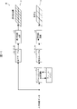
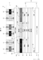
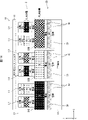
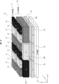
- FIG. 1 is a cross-sectional view of a display device according to Embodiment 1; FIG. It is the top view which looked at the said display apparatus from the viewing surface side. It is a principal part perspective view of the said display apparatus. It is a top view which shows the pixel structure of the said display apparatus.
- FIG. 4 is a plan view showing another pixel structure of the display device;
- FIG. 9 is a plan view showing still another pixel structure of the display device;
- 2 is a system block diagram of the display device;
- FIG. It is a timing chart showing the operation of the display device.
- 10 is a system block diagram of a display device according to Embodiment 2; FIG. It is a timing chart showing the operation of the display device.
- FIG. 4 is a plan view showing another pixel structure of the display device
- FIG. 9 is a plan view showing still another pixel structure of the display device
- 2 is a system block diagram of the display device
- FIG. 10 is a system block diagram of a display
- FIG. 10 is a system block diagram of a display device according to Embodiment 3; It is a timing chart showing the operation of the display device.
- FIG. 11 is a cross-sectional view of a display device according to Embodiment 4;
- FIG. 11 is a cross-sectional view of a display device according to Embodiment 5; It is a principal part perspective view of the said display apparatus. It is a principal part perspective view of the modification of the said display apparatus.
- FIG. 1 is a cross-sectional view of a display device 1 according to Embodiment 1.
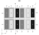
- FIG. 2 is a plan view of the display device 1 viewed from the viewing surface side.
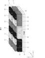
- FIG. 3 is a perspective view of a main portion of the display device 1.
- the display device 1 includes a transparent light-emitting layer 2 provided on the viewing surface 17 side, and a display layer 3 provided on the side opposite to the viewing surface 17 .
- the display layer 3 is formed on the TFT substrate 18 .
- An insulating layer 19 is formed on the display layer 3 .
- a transparent light-emitting layer 2 is formed on the insulating layer 19 .
- the transparent light-emitting layer 2 includes first light-emitting pixels that are adjacent to each other along a first direction (X-direction) parallel to the viewing surface 17 to emit a first color (green) and a second color (red) that are different from each other. It has L1 and a second luminescent pixel L2.
- the display layer 3 is arranged corresponding to the first light emitting pixel L1 and the second light emitting pixel L2 to emit a third color (blue) different from the first color (green) and the second color (red). It has a first display pixel D1 and a second display pixel D2 adjacent to the first display pixel D1 along the X direction for emitting a first color (green).
- the transparent light-emitting layer 2 further includes third light-emitting pixels L3 and fourth light-emitting pixels L4 arranged corresponding to the second display pixels D2 to emit light of a second color (red) and a third color (blue), respectively. have.
- the first luminescent pixel L1 and the fourth luminescent pixel L4 are adjacent to each other along the X direction.
- the display layer 3 further has a third display pixel D3 adjacent to the second display pixel D2 along the X direction for emitting a second color (red).
- the transparent light-emitting layer 2 further includes a fifth light-emitting pixel L5 and a sixth light-emitting pixel L6 arranged corresponding to the third display pixel D3 to emit light of a first color (green) and a third color (blue), respectively. have.
- the first display pixels D1 are arranged adjacent to each other along the Y direction.
- the second display pixels D2 are arranged adjacent to each other along the Y direction.
- the third display pixels D3 are arranged adjacent to each other along the Y direction.
- the first luminescent pixels L1 are arranged adjacent to each other along the Y direction.
- the second light emitting pixels L2 are arranged adjacent to each other along the Y direction.
- the third light emitting pixels L3 are arranged adjacent to each other along the Y direction.
- the fourth light emitting pixels L4 are arranged adjacent to each other along the Y direction.
- the fifth light emitting pixels L5 are arranged adjacent to each other along the Y direction.
- the sixth light emitting pixels L6 are arranged adjacent to each other along the Y direction.
- Each of the first to sixth luminescent pixels L1, L2, L3, L4, L5, and L6 and the first to third display pixels D1, D2, and D3 is formed between a pair of electrodes.
- a quantum dot layer electrophotonescence emitting layer
- hole transport layer formed between one of the pair of electrodes and the quantum dot layer
- pair of electrodes formed between the other and the quantum dot layer and an electron transport layer.
- the transparent light-emitting layer 2 includes first to sixth light-emitting pixels L1 to L6 including quantum dot layers that are transparent and capable of self-luminescence.
- the display layer 3 may be transparent or opaque. Moreover, the display layer 3 may be provided with a self-luminous element, or may be a panel provided with a liquid crystal display element and a backlight.
- the transparent light-emitting layer 2 is provided on the viewing surface 17 side of the display device 1, and the display layer 3 is provided on the side opposite to the viewing surface 17.
- the transparent light emitting layer 2 and the display layer 3 may be composed of organic or inorganic LEDs (Light Emitting Diodes).
- the transparent light-emitting layer 2 and the display layer 3 may contain QDs (quantum dots).
- the pixels of the display layer 3 are provided corresponding to the plurality of pixels of the transparent light emitting layer 2 . At this time, as shown in FIGS. 2 and 3, the color of the pixels of the transparent light-emitting layer 2 and the color of the pixels of the display layer 3 are made to overlap.
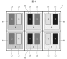
- FIG. 4 is a plan view showing the pixel structure of the display device 1.
- the first light emitting pixel L1 and the second light emitting pixel L2 arranged in the transparent light emitting layer 2 and the first display pixel D1 arranged in the display layer 3 form one RGB pixel.
- the third luminescent pixel L3, the fourth luminescent pixel L4, and the second display pixel D2 constitute one pixel, and the fifth luminescent pixel L5, the sixth luminescent pixel L6, and the third display pixel D3 constitute one pixel. do.
- 6 pixels of 2 rows and 3 columns are configured.
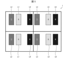
- FIG. 5 is a plan view showing another pixel structure of the display device 1.
- the first luminescent pixel L1, the second luminescent pixel L2, and the fourth luminescent pixel L4 arranged in the transparent luminescent layer 2 form one RGB pixel.
- a third light emitting pixel L3, a fifth light emitting pixel L5, and a sixth light emitting pixel L6 arranged in the transparent light emitting layer 2 form one pixel.
- 4 pixels of 2 rows and 2 columns are configured.
- FIG. 6 is a plan view showing still another pixel structure of the display device 1.
- the first display pixel D1, the second display pixel D2, and the third display pixel D3 arranged on the display layer 3 form one RGB pixel.
- two pixels of two rows and one column are configured.
- first and second light-emitting pixels L1 and L2 of the upper left transparent light-emitting layer 2 and the first display pixel D1 of the display layer 3 are one pixel, and the third and fourth light-emitting pixels L3 of the right transparent light-emitting layer 2 are arranged. If L4 and the second display pixel D2 of the display layer 3 are regarded as one pixel, it is possible to display a total of 6 pixels, ie, 3 pixels horizontally and 2 pixels vertically, as shown in FIG.
- the pixel structure shown in FIG. 4 is the pixel structure with the highest definition.
- FIG. 7 is a system block diagram of the display device 1.
- FIG. 8 is a timing chart showing the operation of the display device 1.
- FIG. 7 is a system block diagram of the display device 1.
- FIG. 8 is a timing chart showing the operation of the display device 1.
- the input image data is decomposed into three color components, for example, R (red component)/G (green component)/B (blue component), and the pixels arranged in the transparent light emitting layer 2 display R and G
- R red component
- G green component
- B blue component
- the pixels arranged on the display layer 3 display B and the pixels on the transparent light-emitting layer 2 display B and R the pixels on the display layer 3 display G and the pixels on the transparent light-emitting layer 2 display G and B.
- the counter 20 and the selectors 21, 22, and 23 should be provided so that the pixels of the display layer 3 display R.
- the transparent light emitting layer 2 are displayed as (R0, G0), (B1, R1), (G2, B2), and the display layer 3 is controlled to be displayed as (B0), (G1), (R2).
- the intensity and characteristics of the light may differ. It is better to provide different correction tables for the transparent light-emitting layer 2 and the display layer 3 so as to make the corrections visible.
- the display device 1 has an R terminal that receives pixel data R0 of input video data via a correction table 24, a B terminal that receives pixel data B0 of input video data via a correction table 25, Selectors 21 and 22 each having a G terminal for receiving pixel data G0 of input video data via a correction table 26, an R terminal for receiving pixel data R1 of input video data via a correction table 29, A selector 23 having a B terminal for receiving pixel data B1 via a correction table 27 and a G terminal for receiving pixel data G1 of input video data via a correction table 28, and selectors 21 and 22 for receiving count values of input video data.
- a light emission driving circuit 13 that drives the first to sixth light emitting pixels L1 to L6 arranged in the transparent light emitting layer 2 based on the output of the selector 21 and the output of the selector 22, and the selector and a display drive circuit 14 for driving the first to third display pixels D1 to D3 arranged on the display layer 3 based on the output of 23 .
- the pixels of one layer are lighted. Brightness is improved in comparison.
- one pixel When viewed from the front of the display device 1, one pixel can be configured with a region of two sub-pixels (for example, two of the first light-emitting pixel L1 and the second light-emitting pixel L2). Therefore, the input image data can be displayed with a resolution 1.5 times higher than that of the transparent light emitting layer 2.
- FIG. 1 When viewed from the front of the display device 1, one pixel can be configured with a region of two sub-pixels (for example, two of the first light-emitting pixel L1 and the second light-emitting pixel L2). Therefore, the input image data can be displayed with a resolution 1.5 times higher than that of the transparent light emitting layer 2.
- the data transfer amount may be small and the frame time may be shortened. Specifically, it will be described in detail in the second and subsequent embodiments. Therefore, moving images can be rewritten at high speed as rough images using the pixels of the lower display layer 3 . Then, the still image is slowly rewritten as a fine image using the pixels of the transparent light emitting layer 2 on the upper side.
- FIG. 9 is a system block diagram of the display device 1A according to the second embodiment.
- FIG. 10 is a timing chart showing the operation of the display device 1A. The components described above are given the same reference numerals and detailed description thereof will not be repeated.
- the frame time which is the period of the vertical synchronization signal, is the same for the pixels of the display layer 3 and the pixels of the transparent light emitting layer 2 .
- the frame time can be shortened if the band is the same. Therefore, as a second embodiment, an example in which the frame rate is changed between the transparent light-emitting layer 2 and the display layer 3 is given, and FIG. 9 is a system block diagram, and FIG. 10 is a timing chart.
- a frame time (display frame time) for driving the first display pixels D1 arranged on the display layer 3 is a frame time (light emission frame time) for driving the first light emitting pixels L1 arranged on the transparent light emitting layer 2. ).
- the display drive circuit 14 drives the first to third display pixels D1 to D3 arranged on the display layer 3 based on the input video data.
- the light emission driving circuit 13 drives the first to sixth light emitting pixels L1 to L6 arranged in the transparent light emitting layer 2 based on the input image data.
- the display device 1A further includes a frame memory 15 arranged in front of the light emission drive circuit 13 in order to lengthen the frame time (light emission frame time) of the input image data for the first to sixth light emission pixels L1 to L6. .
- FIG. 9 and 10 show the case of inputting the input video data in half the frame time of FIG.
- a 120 Hz video signal is input to a panel whose original specification is 60 Hz input.
- Data is transmitted to the display layer 3 at the frame time of the input video data and displayed. Since the transparent light emitting layer 2 cannot transmit data at that frame rate, the input video data is temporarily stored in the frame memory 15 as shown in FIG. 9, and the frame time is doubled before transmission. In that case, since it is necessary to transmit two frames of input video data in one frame time, one frame may be thinned out or an average of two frames may be obtained.
- an input image of three consecutive pixels in the n-th frame is (R0(n), G0(n), B0(n)), (R1(n), G1(n), B1(n)) , (R2(n), G2(n), B2(n)), the displayed values are:
- the display device 1A includes a display drive circuit 14 that drives the first display pixels D1 based on the input video data, a light emission drive circuit 13 that drives the first light emission pixels L1 based on the input video data, and the input video data. and a frame memory 15 arranged in front of the light emission driving circuit 13 in order to lengthen the light emission frame time.
- FIG. 11 is a system block diagram of the display device 1B according to the third embodiment.
- FIG. 12 is a timing chart showing the operation of the display device 1B. The components described above are given the same reference numerals and detailed description thereof will not be repeated.
- the display device 1B includes a display driving circuit 14 that drives the first to third display pixels D1 to D3 of the display layer 3 based on input video data, and a display driving circuit 14 that drives the first to sixth display pixels D1 to D3 of the transparent light emitting layer 2 based on the input video data.
- a light emission drive circuit 13 that drives the light emission pixels L1 to L6, and a frame rate conversion circuit 16 and a frame memory 15 arranged before the display drive circuit 14 in order to shorten the frame time (display frame time) of the input video data. further provide.
- Embodiment 2 the frame time of the input video data is halved.
- the frame rate conversion circuit 16 generates video data with half the frame time and displays it on the display layer 3 is shown.
- FIGS. 11 and 12 input video data having the same frame time as in FIG. 8 is input, and the frame rate conversion circuit 16 generates video data with half the frame time.
- the frame rate conversion circuit 16 may output the same video data twice, or may output video data temporally interpolated by predicting motion.
- the display layer 3 transmits video data with half the frame time generated by the frame rate conversion circuit 16 .
- the display device 1B includes the display drive circuit 14 that drives the first display pixels D1 based on the input video data, the light emission drive circuit 13 that drives the first light emission pixels L1 based on the input video data, and the input It further includes a frame rate conversion circuit 16 arranged in front of the display drive circuit 14 in order to shorten the display frame time of the video data.
- the frame rate conversion circuit 16 Since the frame rate conversion circuit 16 only needs to convert the video data of the display layer 3, the number of pixels corresponding to the video data to be converted can be reduced compared to the case where the video data of the transparent light emitting layer 2 is also converted. In the example of the present embodiment, since it is sufficient to convert 1/3 of the data amount, the capacity of the frame memory 15 and arithmetic processing can be reduced to 1/3 compared to the case where all the input video data are subjected to frame rate conversion. In this manner, compared to a monitor having a conventional frame rate conversion circuit 16, it is possible to achieve both high definition and a high frame rate while reducing resources such as memory and circuits.
- FIG. 13 is a cross-sectional view of a display device 1C according to Embodiment 4.
- FIG. The components described above are given the same reference numerals and detailed description thereof will not be repeated.
- the display device 1C includes a transparent light-emitting layer 2 provided on the viewing surface 17 side, and a display layer 3C provided on the side opposite to the viewing surface 17.
- the display layer 3C has a liquid crystal panel 30 and a backlight 31 provided on the side opposite to the viewing surface 17 of the liquid crystal panel 30 .
- the liquid crystal panel 30 includes a pair of polarizing plates 31, color filters 33B formed between the polarizing plates 31 corresponding to the first and second light emitting pixels L1 and L2 for transmitting blue light, and green light.
- Color filters 33G formed between the polarizing plates 31 corresponding to the third and fourth light emitting pixels L3 and L4 to transmit red light, and the fifth and sixth light emitting pixels L5 and L6 to transmit red light.
- a pair of glass substrates 34 arranged between the color filters 33R, 33G, and 33B and the polarizing plates 31, and a pair of glass substrates 34 corresponding to the color filters 33B.
- the backlight 31 includes a backlight board 37 and a light source 38 arranged on the backlight board 37 .
- the color filter 33B, the pair of electrodes 35B, the liquid crystal layer 36, and the backlight 31 constitute the first display pixel D1C.
- the color filter 33G, the pair of electrodes 35G, the liquid crystal layer 36, and the backlight 31 constitute the second display pixel D2C.
- the color filter 33R, the pair of electrodes 35R, the liquid crystal layer 36, and the backlight 31 constitute a third display pixel D3C.
- the structure of the display device 1C viewed from the viewing surface 17 side is the same as the structure shown in FIG. 2 of the first embodiment.
- the structure of the display device 1C viewed obliquely is the same as the structure shown in FIG.
- the backlight 31 may be composed of a sheet containing a light-emitting portion that emits blue light and ultraviolet light, phosphors, and quantum dots (QDs).
- the frame rate is increased by making the frame time shorter than the frame times of the first to sixth light emitting pixels L1 to L6 of the transparent light emitting element 2. can produce a remarkable effect.
- FIG. 14 is a cross-sectional view of a display device 1D according to the fifth embodiment.
- FIG. 15 is a perspective view of a main portion of the display device 1D. The components described above are given the same reference numerals and detailed description thereof will not be repeated.
- the display device 1D includes a transparent light-emitting layer 2 provided on the viewing surface 17 side, and a display layer 3D provided on the side opposite to the viewing surface 17.
- the display layer 3D includes a first light-emitting pixel L1 and a second light-emitting pixel L1 and a second light-emitting pixel L1 for emitting a third color (blue) different from the first color (green) and the second color (red) by photoluminescence (PL).
- a first display pixel D1D arranged corresponding to the pixel L2; and a third display pixel D3D adjacent to the second display pixel D2D along the X direction to emit two colors (red) by PL.
- the second display pixel D2D is arranged corresponding to the third and fourth light emitting pixels L3 and L4.
- the third display pixel D3D is arranged corresponding to the fifth and sixth light emitting pixels L5 and L6.
- the display layer 3D includes an ultraviolet light source 39 that supplies ultraviolet rays to the first display pixels D1D, an ultraviolet light source 39 that supplies ultraviolet rays to the second display pixels D2D, and an ultraviolet light source 39 that supplies ultraviolet rays to the first display pixels D3D. Including further. Electrodes 40 are provided on both sides of each ultraviolet light source 39 . The first to third display pixels D1D to D3D emit light based on the ultraviolet rays supplied from each ultraviolet light source 39. FIG.
- An ultraviolet cut filter 41 for absorbing ultraviolet rays supplied from the ultraviolet light source 39 is provided on the side of the transparent light emitting layer 2 opposite to the display layer 3D.
- the display device 1D according to the fifth embodiment uses quantum dots in both the transparent light-emitting layer 2 and the display layer 3D, and therefore has wide color reproducibility. Since the first to sixth light emitting pixels L1 to L6 using quantum dots are provided in the transparent light emitting layer 2, high transmittance can be obtained.
- the first to third display pixels D1D to D3D of the display layer 3D are excited by ultraviolet rays to emit light, the brightness can be increased and deterioration is small.
- FIG. 16 is a perspective view of main parts of a display device 1E according to a modification. The components described above are given the same reference numerals and detailed description thereof will not be repeated.
- the display device 1D includes a transparent light-emitting layer 2 and a display layer 3E.
- the display layer 3E includes first display pixels D1E arranged corresponding to two first light-emitting pixels L1 and two second light-emitting pixels L2 for emitting a third color (blue) by PL;
- a second display pixel D2E arranged corresponding to two third light emitting pixels L3 and two fourth light emitting pixels L4 to emit one color (green) by PL, and a second color (red).
- It includes third display pixels D3E arranged corresponding to two fifth light emitting pixels L5 and two sixth light emitting pixels L6 to emit PL light.
- the first to third display pixels D1E to D3E may be connected over four luminescent pixels.
- the areas of the first to third display pixels D1E to D3E for PL emission are larger than the areas of the first to third display pixels D1D to D3D, which facilitates the application of QDs during manufacturing.
- the display device 1E according to Embodiment 5 uses quantum dots in both the transparent light-emitting layer 2 and the display layer 3E, so that the color gamut can be widened. In addition, it is also possible to share the QD material in a region corresponding to four light-emitting pixels of 2 rows ⁇ 2 columns during manufacturing.
- the present invention is not limited to the above-described embodiments, but can be modified in various ways within the scope of the claims, and can be obtained by appropriately combining technical means disclosed in different embodiments. is also included in the technical scope of the present invention. Furthermore, new technical features can be formed by combining the technical means disclosed in each embodiment.
Landscapes
- Engineering & Computer Science (AREA)
- Physics & Mathematics (AREA)
- General Physics & Mathematics (AREA)
- Theoretical Computer Science (AREA)
- Computer Hardware Design (AREA)
- Chemical & Material Sciences (AREA)
- Crystallography & Structural Chemistry (AREA)
- Microelectronics & Electronic Packaging (AREA)
- Inorganic Chemistry (AREA)
- Devices For Indicating Variable Information By Combining Individual Elements (AREA)
- Electroluminescent Light Sources (AREA)
Abstract
Description
図1は実施形態1に係る表示装置1の断面図である。図2は表示装置1を視認面側からみた平面図である。図3は表示装置1の要部斜視図である。
図9は実施形態2に係る表示装置1Aのシステムブロック図である。図10は表示装置1Aの動作を示すタイミングチャートである。前述した構成要素には同様の参照符号を付し、その詳細な説明は繰り返さない。
表示層3:(B0(2n))、(G1(2n))、(R2(2n))、
透明発光層2:((R0(2n)+R0(2n+1))/2、(G0(2n)+G0(2n+1))/2)、((B1(2n)+B1(2n+1))/2、(R1(2n)+R1(2n+1))/2)、((G2(2n)+G2(2n+1))/2、(B2(2n)+B2(2n+1))/2)、
(2n+1)フレーム目、
表示層3:(B0(2n+1))、(G1(2n+1))、(R2(2n+1))、
透明発光層:(2n)フレーム目と同じ、
このように、第1表示画素D1を駆動するための表示フレーム時間が、第1発光画素L1を駆動するための発光フレーム時間よりも短い。
図11は実施形態3に係る表示装置1Bのシステムブロック図である。図12は表示装置1Bの動作を示すタイミングチャートである。前述した構成要素には同様の参照符号を付し、その詳細な説明は繰り返さない。
図13は実施形態4に係る表示装置1Cの断面図である。前述した構成要素には同様の参照符号を付し、その詳細な説明は繰り返さない。
図14は実施形態5に係る表示装置1Dの断面図である。図15は表示装置1Dの要部斜視図である。前述した構成要素には同様の参照符号を付し、その詳細な説明は繰り返さない。
2 透明発光層
3 表示層
L1 第1発光画素
L2 第2発光画素
L3 第3発光画素
L4 第4発光画素
L5 第5発光画素
L6 第6発光画素
D1 第1表示画素
D2 第2表示画素
D3 第3表示画素
D1D 第1表示画素
D2D 第2表示画素
D3D 第3表示画素
D1E 第1表示画素
D2E 第2表示画素
D3E 第3表示画素
13 発光駆動回路
14 表示駆動回路
15 フレームメモリ
16 フレームレート変換回路
30 液晶パネル
31 バックライト
39 紫外線光源
Claims (12)
- 視認面側に設けられた透明発光層と、
前記視認面と反対側に設けられた表示層とを備え、
前記透明発光層が、互いに異なる第1色及び第2色をそれぞれ発光するために前記視認面に平行な第1方向に沿って互いに隣接する第1発光画素及び第2発光画素を有し、
前記表示層が、前記第1色及び前記第2色とは異なる第3色を発光するために前記第1発光画素及び前記第2発光画素に対応して配置される第1表示画素と、前記第1色を発光するために前記第1方向に沿って前記第1表示画素に隣接する第2表示画素とを有し、
前記透明発光層が、前記第2色及び前記第3色をそれぞれ発光するために前記第2表示画素に対応して配置される第3発光画素及び第4発光画素をさらに有する表示装置。 - 前記第1発光画素と前記第4発光画素とが、前記第1方向に沿って互いに隣接する請求項1に記載の表示装置。
- 前記表示層が、前記第2色を発光するために前記第1方向に沿って前記第2表示画素に隣接する第3表示画素をさらに有し、
前記透明発光層が、前記第1色及び前記第3色をそれぞれ発光するために前記第3表示画素に対応して配置される第5発光画素及び第6発光画素をさらに有する請求項1又は2に記載の表示装置。 - 前記第1表示画素を駆動するための表示フレーム時間が、前記第1発光画素を駆動するための発光フレーム時間よりも短い請求項1から3の何れか一項に記載の表示装置。
- 入力映像データに基づいて前記第1表示画素を駆動する表示駆動回路と、
前記入力映像データに基づいて前記第1発光画素を駆動する発光駆動回路と、
前記入力映像データの前記発光フレーム時間を長くするために前記発光駆動回路の前段に配置されたフレームメモリとをさらに備える請求項4の何れか一項に記載の表示装置。 - 入力映像データに基づいて前記第1表示画素を駆動する表示駆動回路と、
前記入力映像データに基づいて前記第1発光画素を駆動する発光駆動回路と、
前記入力映像データの前記表示フレーム時間を短くするために前記表示駆動回路の前段に配置されたフレームレート変換回路とをさらに備える請求項4又は5に記載の表示装置。 - 前記第1から前記第3表示画素のぞれぞれが、前記第1方向に交差する第2方向に沿って互いに隣接して配置され、
前記第1から前記第6発光画素のそれぞれが、前記第2方向に沿って互いに隣接して配置される請求項3に記載の表示装置。 - 前記第1発光画素が、一対の電極と、前記一対の電極の間に形成された量子ドット層と、前記一対の電極の一方と前記量子ドット層との間に形成された正孔輸送層と、前記一対の電極の他方と前記量子ドット層との間に形成された電子輸送層とを含む請求項1から7の何れか一項に記載の表示装置。
- 前記第1発光画素が、有機又は無機のエレクトロルミネッセンス発光層を含む請求項1から7の何れか一項に記載の表示装置。
- 前記第1表示画素が、有機又は無機のエレクトロルミネッセンス発光層を含む請求項1から9の何れか一項に記載の表示装置。
- 前記第1表示画素が、液晶パネルとバックライトとを含む請求項1から9の何れか一項に記載の表示装置。
- 前記第1表示画素が、光ルミネセンスにより発光し、前記第1表示画素に紫外線を供給する紫外線光源とを含む請求項1から9の何れか一項に記載の表示装置。
Priority Applications (3)
| Application Number | Priority Date | Filing Date | Title |
|---|---|---|---|
| PCT/JP2021/031744 WO2023032002A1 (ja) | 2021-08-30 | 2021-08-30 | 表示装置 |
| US18/573,023 US12495690B2 (en) | 2021-08-30 | 2021-08-30 | Display device |
| JP2023544810A JP7623507B2 (ja) | 2021-08-30 | 2021-08-30 | 表示装置 |
Applications Claiming Priority (1)
| Application Number | Priority Date | Filing Date | Title |
|---|---|---|---|
| PCT/JP2021/031744 WO2023032002A1 (ja) | 2021-08-30 | 2021-08-30 | 表示装置 |
Publications (1)
| Publication Number | Publication Date |
|---|---|
| WO2023032002A1 true WO2023032002A1 (ja) | 2023-03-09 |
Family
ID=85412329
Family Applications (1)
| Application Number | Title | Priority Date | Filing Date |
|---|---|---|---|
| PCT/JP2021/031744 Ceased WO2023032002A1 (ja) | 2021-08-30 | 2021-08-30 | 表示装置 |
Country Status (3)
| Country | Link |
|---|---|
| US (1) | US12495690B2 (ja) |
| JP (1) | JP7623507B2 (ja) |
| WO (1) | WO2023032002A1 (ja) |
Citations (3)
| Publication number | Priority date | Publication date | Assignee | Title |
|---|---|---|---|---|
| JP2006147555A (ja) * | 2004-11-23 | 2006-06-08 | Samsung Sdi Co Ltd | 有機電界発光表示素子及びその製造方法 |
| JP2018013622A (ja) * | 2016-07-21 | 2018-01-25 | 株式会社半導体エネルギー研究所 | 表示装置、および電子機器 |
| JP2018022133A (ja) * | 2016-05-30 | 2018-02-08 | マブン オプトロニックス カンパニー リミテッドMaven Optronics Co., Ltd. | フォトルミネセンス表示装置およびその製造方法 |
Family Cites Families (5)
| Publication number | Priority date | Publication date | Assignee | Title |
|---|---|---|---|---|
| JP4868021B2 (ja) | 2009-01-07 | 2012-02-01 | ソニー株式会社 | 固体撮像素子および駆動制御方法 |
| JP2013243048A (ja) | 2012-05-21 | 2013-12-05 | Canon Inc | 表示パネル、表示装置、および表示パネルの製造方法 |
| US10620478B2 (en) | 2016-05-30 | 2020-04-14 | Maven Optronics Co., Ltd. | Photoluminescent display device and method for manufacturing the same |
| KR20250033414A (ko) * | 2023-08-29 | 2025-03-10 | 삼성디스플레이 주식회사 | 표시 장치 |
| KR20250085872A (ko) * | 2023-12-05 | 2025-06-13 | 삼성디스플레이 주식회사 | 표시 장치 |
-
2021
- 2021-08-30 JP JP2023544810A patent/JP7623507B2/ja active Active
- 2021-08-30 US US18/573,023 patent/US12495690B2/en active Active
- 2021-08-30 WO PCT/JP2021/031744 patent/WO2023032002A1/ja not_active Ceased
Patent Citations (3)
| Publication number | Priority date | Publication date | Assignee | Title |
|---|---|---|---|---|
| JP2006147555A (ja) * | 2004-11-23 | 2006-06-08 | Samsung Sdi Co Ltd | 有機電界発光表示素子及びその製造方法 |
| JP2018022133A (ja) * | 2016-05-30 | 2018-02-08 | マブン オプトロニックス カンパニー リミテッドMaven Optronics Co., Ltd. | フォトルミネセンス表示装置およびその製造方法 |
| JP2018013622A (ja) * | 2016-07-21 | 2018-01-25 | 株式会社半導体エネルギー研究所 | 表示装置、および電子機器 |
Also Published As
| Publication number | Publication date |
|---|---|
| US20240292696A1 (en) | 2024-08-29 |
| US12495690B2 (en) | 2025-12-09 |
| JP7623507B2 (ja) | 2025-01-28 |
| JPWO2023032002A1 (ja) | 2023-03-09 |
Similar Documents
| Publication | Publication Date | Title |
|---|---|---|
| KR100649246B1 (ko) | 역다중화 장치와, 이를 이용한 표시 장치 및 그 표시 패널 | |
| KR101531764B1 (ko) | 표시장치 | |
| CN101317212B (zh) | 用于驱动显示元件的显示设备和方法 | |
| JP4702459B2 (ja) | 液晶表示装置組立体、及び、液晶表示装置組立体の駆動方法 | |
| JP4869661B2 (ja) | 表示装置 | |
| TWI624821B (zh) | 微型發光二極體顯示面板及其驅動方法 | |
| JP2006301043A (ja) | ディスプレイ装置 | |
| JP2012018386A (ja) | 表示装置および駆動方法 | |
| WO2017028439A1 (zh) | 3d显示装置及其驱动方法 | |
| WO2012111471A1 (ja) | 表示装置 | |
| JP2015099331A (ja) | 液晶表示装置 | |
| JP2004138827A5 (ja) | ||
| US20110122176A1 (en) | Display device | |
| US20090059581A1 (en) | Display Device | |
| JP2002198174A (ja) | カラー有機elディスプレイ及びその駆動方法 | |
| JP4650726B2 (ja) | 表示装置 | |
| JP2010002755A (ja) | 表示装置 | |
| JP7623507B2 (ja) | 表示装置 | |
| KR102372062B1 (ko) | 표시 장치 | |
| JP2020008662A (ja) | 表示装置 | |
| TWI646521B (zh) | 顯示裝置及其驅動方法 | |
| KR100567177B1 (ko) | 반도체 구동 회로, 디스플레이 장치, 및 디스플레이장치의 휘도 평형 조절 방법 | |
| JP2022132062A (ja) | 画像表示方法及び画像表示装置 | |
| JP2002208485A (ja) | 有機ledディスプレイ | |
| WO2015107723A1 (ja) | 表示装置 |
Legal Events
| Date | Code | Title | Description |
|---|---|---|---|
| 121 | Ep: the epo has been informed by wipo that ep was designated in this application |
Ref document number: 21955899 Country of ref document: EP Kind code of ref document: A1 |
|
| WWE | Wipo information: entry into national phase |
Ref document number: 2023544810 Country of ref document: JP |
|
| WWE | Wipo information: entry into national phase |
Ref document number: 18573023 Country of ref document: US |
|
| NENP | Non-entry into the national phase |
Ref country code: DE |
|
| 122 | Ep: pct application non-entry in european phase |
Ref document number: 21955899 Country of ref document: EP Kind code of ref document: A1 |