WO2023026712A1 - 回折格子結合器 - Google Patents
回折格子結合器 Download PDFInfo
- Publication number
- WO2023026712A1 WO2023026712A1 PCT/JP2022/027386 JP2022027386W WO2023026712A1 WO 2023026712 A1 WO2023026712 A1 WO 2023026712A1 JP 2022027386 W JP2022027386 W JP 2022027386W WO 2023026712 A1 WO2023026712 A1 WO 2023026712A1
- Authority
- WO
- WIPO (PCT)
- Prior art keywords
- refractive index
- light
- diffraction grating
- modified refractive
- base material
- Prior art date
- Legal status (The legal status is an assumption and is not a legal conclusion. Google has not performed a legal analysis and makes no representation as to the accuracy of the status listed.)
- Ceased
Links
Images


Classifications
-
- G—PHYSICS
- G02—OPTICS
- G02B—OPTICAL ELEMENTS, SYSTEMS OR APPARATUS
- G02B5/00—Optical elements other than lenses
- G02B5/18—Diffraction gratings
- G02B5/1866—Transmission gratings characterised by their structure, e.g. step profile, contours of substrate or grooves, pitch variations, materials
-
- G—PHYSICS
- G02—OPTICS
- G02B—OPTICAL ELEMENTS, SYSTEMS OR APPARATUS
- G02B5/00—Optical elements other than lenses
- G02B5/18—Diffraction gratings
-
- G—PHYSICS
- G02—OPTICS
- G02B—OPTICAL ELEMENTS, SYSTEMS OR APPARATUS
- G02B6/00—Light guides; Structural details of arrangements comprising light guides and other optical elements, e.g. couplings
- G02B6/10—Light guides; Structural details of arrangements comprising light guides and other optical elements, e.g. couplings of the optical waveguide type
- G02B6/12—Light guides; Structural details of arrangements comprising light guides and other optical elements, e.g. couplings of the optical waveguide type of the integrated circuit kind
- G02B6/122—Basic optical elements, e.g. light-guiding paths
-
- H—ELECTRICITY
- H01—ELECTRIC ELEMENTS
- H01S—DEVICES USING THE PROCESS OF LIGHT AMPLIFICATION BY STIMULATED EMISSION OF RADIATION [LASER] TO AMPLIFY OR GENERATE LIGHT; DEVICES USING STIMULATED EMISSION OF ELECTROMAGNETIC RADIATION IN WAVE RANGES OTHER THAN OPTICAL
- H01S5/00—Semiconductor lasers
- H01S5/02—Structural details or components not essential to laser action
- H01S5/022—Mountings; Housings
- H01S5/0225—Out-coupling of light
-
- H—ELECTRICITY
- H01—ELECTRIC ELEMENTS
- H01S—DEVICES USING THE PROCESS OF LIGHT AMPLIFICATION BY STIMULATED EMISSION OF RADIATION [LASER] TO AMPLIFY OR GENERATE LIGHT; DEVICES USING STIMULATED EMISSION OF ELECTROMAGNETIC RADIATION IN WAVE RANGES OTHER THAN OPTICAL
- H01S5/00—Semiconductor lasers
- H01S5/50—Amplifier structures not provided for in groups H01S5/02 - H01S5/30
Definitions
- the present invention relates to a grating coupler that optically couples optical elements such as optical integrated circuits and optical fibers using a diffraction grating.
- a diffraction grating coupler equipped with a diffraction grating formed by periodically forming grooves, holes, etc. in a plate-shaped base material. It is In such a diffraction grating coupler, light having a specific wavelength corresponding to the period of grooves, holes, etc., among the light input (incident) from the end face of the base material (hereinafter simply referred to as "end face”) is The light is diffracted and output (emitted) from the surface of the base material (hereinafter simply referred to as "surface”).
- Non-Patent Document 1 describes a diffraction grating coupler in which holes are arranged in a square lattice in a plate-like base material made of Si provided on a substrate made of SiO 2 .
- the vacancies having a trapezoidal planar shape are arranged so that one of the two directions in which the lattice points of the square lattice are arranged (perpendicular to each other) is parallel to the upper and lower bases of the trapezoid.
- a grating coupler referred to as a “trapezoidal hole type”
- a hole having an isosceles triangle plane shape are arranged so that one of the two directions is parallel to the base of the isosceles triangle Grid couplers (“isosceles triangular hole type”) have been fabricated.
- the trapezoidal hole type is more efficient in coupling with an external optical element than the isosceles triangular hole type.
- the diffraction of light occurs mainly at the base of the isosceles triangle of each hole, whereas the electric field of light tends to be concentrated near the apex angle of each hole.
- the efficiency of coupling with external optical elements is also less efficient, and thus the efficiency of coupling with external optical elements is also less.
- the concentration of the electric field is less likely to occur than in the case of the isosceles triangular hole type, and the electric field intensity can be made relatively high near the base where light diffraction mainly occurs.
- the efficiency of diffraction and the efficiency of coupling with external optical elements can be made higher than in the case of the isosceles triangular hole type.
- Non-Patent Document 1 when light is input from the end face, part of the light input from the end face is formed by grooves or holes in both the trapezoidal hole type and the isosceles triangular hole type. Reflection produces reflected light whose traveling direction is changed by 180°, and the reflected light is emitted from the end surface. Thus, when the reflected light is emitted from the end face, the efficiency of light output from the surface is lowered. In addition, there is a possibility that the emitted light may enter (reversely enter) the optical element on the input side, causing the optical element on the input side to malfunction.
- the light when light is input from the surface, the light is mainly directed from the longer side to the shorter side of the lower and upper bases of the trapezoidal holes in the base material (in the case of trapezoidal holes), or It proceeds from the base side of the isosceles triangle to the apex side (in the case of the isosceles triangle cavity type), but it can also proceed in a direction 180° different from that. In this way, light traveling in directions different by 180° results in loss.
- the problem to be solved by the present invention is to provide a diffraction grating coupler capable of efficiently outputting input light.
- a diffraction grating coupler which has been made to solve the above problems, A plate-shaped base material, and dots periodically arranged two-dimensionally or one-dimensionally on the base material, or line-shaped bases periodically arranged one-dimensionally on the base material
- a diffraction grating having a modified refractive index region that is a region with a different refractive index from the material,
- the modified refractive index region has an absolute value of a first coupling coefficient, which is an index indicating the intensity of reflection of light traveling in a first direction parallel to the base material in a second direction different from the first direction by 180°.
- of the second coupling coefficient which is an index indicating the intensity at which the light traveling in the second direction is reflected in the first direction, to
- the modified refractive index region is a region having a refractive index different from that of the base material, as described above, and is typically composed of air (holes in the case of points, and empty grooves in the case of lines).
- the modified refractive index region may be formed by embedding an object made of a material different from that of the base material in the base material.
- the modified refractive index regions are point-shaped, they are arranged periodically in a two-dimensional (square lattice, rectangular lattice, etc.) or one-dimensional manner, and when the modified refractive index regions are linear, arranges them periodically in one dimension.
- the modified refractive index region may be provided all over the base material in the thickness direction (so as to penetrate the base material), or may be provided only partially in the thickness direction of the base material. In the latter case, the modified refractive index region may be provided from one surface of the base material (so that it appears on the one surface and does not appear on the other surface), or only inside the base material ( (not appearing on either side of the material).
- the coupling coefficient is an index that indicates the intensity of the light that is diffracted (that is, reflected) in the 180° direction while traveling in the diffraction grating. This 180° reflected light interacts with the light generated by the direct 180° change in the traveling direction of the light by the diffraction grating and the light output perpendicular to the base material (in a direction different from the traveling direction by 90°).
- the first coupling coefficient ⁇ 1 is an index indicating the intensity of light that is reflected by 180° (in the second direction) from the light traveling in a predetermined first direction within the diffraction grating
- the second coupling coefficient ⁇ 2 is: It is an index that indicates the intensity of light that is reflected 180° (in the first direction) from the light traveling in the second direction within the diffraction grating.
- the diffraction grating coupler according to the present invention by having the modified refractive index region having a planar shape in which
- are different values.
- the planar shape of the modified refractive index region does not have 180° rotational symmetry.
- each of the modified refractive index regions includes a first partial modified refractive index region and a second partial modified refractive index region different from the first partial modified refractive index region in either or both of shape and area. It is preferably paired.
- each of the modified refractive index regions includes, in addition to the first partial modified refractive index region and the second partial modified refractive index region, the first partial modified refractive index region or the second partial modified refractive index region may have one or two or more partially modified refractive index regions that differ in either or both of shape and area.
- the first coupling coefficient ⁇ 1 is the second coupling coefficient 180° different from the first direction and the third direction, among the lights traveling in the first direction and the third direction with the same phase and the same amplitude. It is an index indicating the intensity reflected in the direction and the fourth direction with the same phase and the same amplitude.
- the second coupling coefficient ⁇ 2 is the intensity of light reflected in the first direction and the third direction with the same phase and the same amplitude among the lights traveling in the second direction and the fourth direction with the same phase and the same amplitude. It is an index that shows With respect to the first coupling coefficient ⁇ 1 and the second coupling coefficient ⁇ 2, if
- the diffraction grating coupler according to the present invention can further include a light amplification layer for amplifying light of a predetermined wavelength, inside the base material in the diffraction grating or on the surface of the base material.
- the predetermined wavelength is a wavelength corresponding to the periodic length of the arrangement of the modified refractive index regions.
- the wavelength in the diffraction grating (which is shorter than the wavelength in a vacuum if the frequency is the same) should be an integer multiple or an integer fraction of the period length.
- An active layer used in a laser element or the like can be applied to the optical amplification layer.
- a diffraction grating coupler having such an optical amplification layer can be suitably used as an optical amplifier that amplifies input light with the optical amplification layer and outputs the amplified light with high efficiency.
- input light can be efficiently output.
- FIG. 1 is a perspective view showing a diffraction grating coupler that is a first embodiment of the present invention
- FIG. FIG. 2 is a top view showing the diffraction grating coupler of the first embodiment
- FIG. 2 is a cross-sectional view A showing the diffraction grating coupler of the first embodiment
- FIG. 4 is a diagram showing parameters for obtaining a first coupling coefficient and a second coupling coefficient in the diffraction grating coupler of the first embodiment
- FIG. 4 is a diagram showing a mechanism of reflected light generation within a diffraction grating
- a graph showing an example of calculation of the real part R and the imaginary part I of the Hermite coupling coefficient in the diffraction grating coupler of the first embodiment.
- FIG. 5 is a top view showing an example of a modification of the diffraction grating coupler of the first embodiment, in which dot-like modified refractive index regions are arranged one-dimensionally.
- FIG. 11 is a top view showing a structure that can be operated as a waveguide grating coupler in the case of having a modified refractive index region with d and S 1 having the values shown in the example of FIG. 10;
- FIG. 11 is a top view showing a structure that can be operated as a waveguide grating coupler in the case of having a modified refractive index region with d and S 1 having the values shown in the example of FIG. 10;
- FIG. 10 is a top view showing a modified example of the diffraction grating coupler of the first embodiment, in which linear modified refractive index regions are arranged one-dimensionally;
- An optical amplifier that is another modified example of the diffraction grating coupler of the first embodiment, in which the optical amplification layer is provided on the surface of the base material of the diffraction grating (a) and in the base material (b) ) is a sectional view showing FIG.
- FIG. 5 is a top view showing a diffraction grating coupler that is a second embodiment of the present invention;
- FIG. 10 is a diagram showing parameters for obtaining a first coupling coefficient and a second coupling coefficient in the diffraction grating coupler of the second embodiment; A graph showing an example of calculation of the real part R and the imaginary part I of the Hermitian coupling coefficient in the diffraction grating coupler of the second embodiment.
- FIG. 10 is a diagram showing the result of calculating the distribution of the intensity of light and the intensity of reflected light;
- FIG. 1 An embodiment of a diffraction grating coupler according to the present invention will be described with reference to FIGS. 1 to 17.
- FIG. 1 An embodiment of a diffraction grating coupler according to the present invention will be described with reference to FIGS. 1 to 17.
- FIG. 1 An embodiment of a diffraction grating coupler according to the present invention will be described with reference to FIGS. 1 to 17.
- FIG. 1 An embodiment of a diffraction grating coupler according to the present invention will be described with reference to FIGS. 1 to 17.
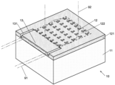
- FIG. 1 shows a perspective view of a diffraction grating coupler 10 according to a first embodiment.
- the diffraction grating coupler 10 comprises a base 11 made of silicon dioxide (SiO 2 ) and having a rectangular planar shape, and a rectangular plate-shaped base material 121 made of silicon (Si) formed on the surface of the base 11 . , a large number of modified refractive index regions 122 made up of holes provided in the base material 121, and one side of the rectangular four sides of the base material 121 (the end on the starting point side in the first direction described later) provided and an input port (optical input unit) 13 .
- the diffraction grating 12 is formed by combining the base material 121 and the modified refractive index region 122 .
- the surface of the base material 121 opposite to the base 11 is a space (air).
- the entire lower surface of the base material 121 is supported by the base 11, but a part of the lower surface of the base material 121 (for example, only two opposite sides of the rectangle of the base material 121) is supported by some member. You can support it.
- the materials of the base 11 and the base material 121 are not limited to the above examples, and other materials may be used.
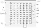
- the modified refractive index region 122 may be formed by embedding a material having a refractive index different from that of the base material 121 in place of the holes. In addition, although several dozen modified refractive index regions 122 are depicted in FIG.
- each of the modified refractive index regions 122 is a second partial modified refractive index region having a planar shape and area different from those of the first partial modified refractive index region 1221 and the first partial modified refractive index region 1221.
- Index regions 1222 are spaced apart from each other.
- the first partial modified refractive index region 1221 is elliptical
- the second partial modified refractive index region 1222 is circular. Since the planar shape and area of the first partial modified refractive index region 1221 and the second partial modified refractive index region 1222 are different, the planar shape of the entire modified refractive index region 122 does not have 180° rotational symmetry. .
- each modified refractive index region 122 is designed so that the ratio
- the first coupling coefficient ⁇ 1 in this embodiment is defined by the light traveling from the input port 13 toward the opposite side of the rectangle of the base material 121 on which the input port 13 is provided (the traveling direction of this light is the “first 2 and 3) is 180° different from the first direction by the modified refractive index region 122 (referred to as the “second direction”). It is an indicator of reflected intensity.
- the second coupling coefficient ⁇ 2 is an index that indicates the intensity with which light traveling in the second direction is reflected in the first direction by the modified refractive index region 122 .
- the planar shape of the first partial modified refractive index region 1221 is elliptical, and the planar shape of the second partial modified refractive index region 1222 is circular. Other shapes are also possible. Also, the second partial modified refractive index region 1222 may differ from the first partial modified refractive index region 1221 only in one of the planar shape and area.
- the modified refractive index regions 122 are arranged one by one on lattice points of the rectangular lattice within a range of the rectangular base material 121 excluding the vicinity of the four sides of the rectangle.
- the two primitive translation vectors of the rectangular lattice are oriented one parallel to the first and second directions and the other perpendicular to the first and second directions.
- the lattice constant of the rectangular lattice is such that the lattice constant a1 in the direction parallel to the first direction and the second direction is longer than the lattice constant a2 in the direction perpendicular to the first direction and the second direction. is set.
- the short axis of the planar shape of the first partial modified refractive index region 1221 is parallel to the first direction and the second direction, and the center of gravity of the first partial modified refractive index region 1221 and the second partial modified refractive index region 1222 are spaced apart in a direction parallel to the first and second directions.
- the modified refractive index region 122 is provided from the upper surface side of the base material 121 to a predetermined depth in the thickness direction without penetrating the base material 121 .
- the modified refractive index region 122 may be formed so as to penetrate the base material 121, or the base material may be The modified refractive index region 122 may be provided only inside 121 .
- the input port 13 is provided in a portion of the rectangular base material 121 on one side of the rectangle where the modified refractive index region 122 is not arranged (the diffraction grating 12 is not formed). This corresponds to the portion between the two grooves 131 extending toward one side of the rectangle.
- An input-side optical element 91 is arranged on the end of the base material 121 outside the input port 13, and an output-side optical element 92 is arranged on the upper surface of the diffraction grating 12 (the surface opposite to the base 11).
- An optical IC or the like can be used for the input side optical element 91, and an optical fiber or the like can be used for the output side optical element 92, respectively.
- the input side optical element 91 is placed at the end of the input port 13 so that the traveling direction of the input light emitted by the input side optical element 91 is parallel to the base material 121 .
- the input light used has a wavelength of the same length as a1 , which is the grating constant of the diffraction grating 12 in the traveling direction of the input light.
- the lattice constant a1 is set according to the wavelength.
- the wavelength of the input light referred to here is the wavelength within the diffraction grating 12, and is shorter than the wavelength in vacuum because the effective refractive index within the diffraction grating 12 is greater than 1.
- Input light input from the input port 13 travels in the diffraction grating 12 in the first direction.
- the input light is diffracted by the periodically arranged modified refractive index regions 122 in the diffraction grating 12 .
- the diffracted light diffracted in the direction perpendicular to the base material 121 is strengthened by interference. .
- the diffracted light diffracted in the direction perpendicular to the base material 121 is extracted from the surface of the base material 121 as output light (FIG. 3).
- an output-side optical element 92 By arranging an output-side optical element 92 on this surface (for example, as shown in FIG. 1, one end of an optical fiber, which is the output-side optical element 92, faces this surface), the output light is transferred to the output-side optical element. Captured in element 92 . Thus, the input side optical element 91 and the output side optical element 92 are optically coupled by the diffraction grating coupler 10 .
- the shape and size of the modified refractive index region 122 are such that the ratio
- the shape and size of the modified refractive index region 122 are designed so that
- the result of simulating the output light and the reflected light in the case of use will be described.
- the design shown below is an example, and even when the modified refractive index regions have other shapes, the first coupling coefficient ⁇ 1 and the second coupling coefficient ⁇ 2 are calculated using the method described in Non-Patent Document 2. Then, it is possible to appropriately design so that
- the base material 121 (Si) has a refractive index of 3.4, and the modified refractive index region 122 (air) has a refractive index of 1.
- the thickness of the base material 121 was 330 nm, and the thickness of the modified refractive index region 122 was 220 nm.
- the wavelength of the input light/output light within the diffraction grating 12 is 470 nm, which is the same value as a1 . Since the effective refractive index of the diffraction grating 12 depends on the size of the modified refractive index regions 122, the wavelengths of the input light and output light in vacuum also differ depending on the size of the modified refractive index regions 122.
- the planar shape of the first partial modified refractive index region 1221 and the planar shape of the second partial modified refractive index region 1222 are determined by the filling factor f 1 of the first partial modified refractive index region 1221 and the filling rate f 1 of the second partial modified refractive index region 1222 .
- the length of the major axis of the ellipse of the first partial modified refractive index region 1221 is fixed to 137 nm, and the filling factor f 1 of the first partial modified refractive index region 1221 is 3.75%, 3.80%, 3.85%, and 3.90%. , 3.95%, the length of the minor axis of the ellipse and the circular diameter of the second partial modified refractive index region 1222 were determined so that the filling factor f of the modified refractive index region 122 was 7%. .
- Non-Patent Document 2 The method described in Non-Patent Document 2 is applied to 15 examples in which the three examples of the distance d between the centers of gravity described above and the examples of the filling factor f 1 of the five first partial modified refractive index regions 1221 are combined. were used to determine the Hermitian coupling coefficient R ⁇ iI and the non-Hermitian coupling coefficient i ⁇ (i is an imaginary unit) for determining the first coupling coefficient ⁇ 1 and the second coupling coefficient ⁇ 2.
- the Hermitian coupling coefficient R ⁇ iI is a coefficient indicating an index that changes the traveling direction of light by 180° without loss, as shown in the frame labeled "Hermitian coupling" in FIG.
- the Hermitian coupling coefficient has a value when changing from the second direction to the first direction (this is R+iI) and a value when changing from the first direction to the second direction (this is R-iI). They have a complex conjugate relationship.
- the non-Hermitian coupling coefficient i ⁇ is a coefficient that indicates an index for changing the traveling direction of light in a direction different from the initial direction by 180°.
- the non-Hermitian coupling coefficient has the same value i ⁇ when changing from the second direction to the first direction and the value when changing from the first direction to the second direction.
- Reflected light is the sum of the light whose traveling direction changes by 180° without loss and the light whose traveling direction changes by 180° with radiation loss.
- the relationship between R1/R2
- FIG. 6 shows the results of calculating the values of R and I in the Hermitian coupling coefficient R ⁇ iI.
- the calculation result of the value ⁇ representing the imaginary part (the real part is 0) of the non-Hermitian coupling coefficient is almost the same value (approximately 70 cm -1 ).
- 15 data points, excluding the two indicated by the dashed arrows, correspond to the distance d between the centers of gravity and the filling factor f of the first partial modified refractive index region 1221. Values of R and I for each of the 15 examples of combinations of 1 are shown.
- the values of the center-of-gravity distance d and the filling factor f 1 of the first partial modified refractive index region 1221 at each data point correspond to the numerical values described on the curves of thin dashed lines that intersect in the vicinity of each data point.
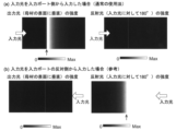
- FIG. 7 shows the output light output in the direction perpendicular to the base material 121 and the output light in the diffraction grating 12 when
- the normal case (a) in which the input light is input from the input port 13 (the input light travels in the first direction) and the input from the end of the base material 121 opposite to the input port 13 are shown for reference. Calculations were performed for two cases (b) when light is input (input light travels in the second direction).
- the modified refractive index region 122 consisting of a pair of the first partial modified refractive index region 1221 and the second partial modified refractive index region 1222 has been described as an example.
- a modified refractive index region consisting of only one region having a refractive index different from that of the base material 121 may be used, or three or more partial modified refractive index regions may be used. You may use the modified refractive index area
- the dot-like modified refractive index regions 122 are two-dimensionally arranged has been shown so far, as shown in FIG. good.
- two light beams extending from the input port 13 are provided.
- the grooves 131 are provided to extend not only to the portion where the modified refractive index region 122 is not arranged, but also to the sides of the partial diffraction grating 13 (where the diffraction grating 12 is not formed) (above and below the diffraction grating 13 in FIG. 8). ing.
- the first partial modified refractive index area 1221 is arranged closer to the input port 13 than the second partial modified refractive index area 1222 , and the minor axis of the elliptical shape of the first partial modified refractive index area 1221 is the groove 131 . is oriented parallel to
- the light is output in a direction perpendicular to the base material 121 while the light passes through the one-dimensional shape between the two grooves 131, in other words, the waveguide-like portion.
- a diffraction grating coupler having such a waveguide-like structure is hereinafter referred to as a "waveguide-type diffraction grating coupler".
- the periodic length (arrangement interval) a of the modified refractive index regions 122 is 0.720 ⁇ m
- the material of the base material 121 is Si (refractive index 3.4)
- the width w of the base material 121 between the two grooves is 0.480 ⁇ m.
- the thickness of the base material 121 is 0.22 ⁇ m.
- the sum S S 1 +S 2 of the area S 1 of the first partial modified refractive index region 1221 and the area S 2 of the second partial modified refractive index region 1222 was 0.08a 2 .
- the ellipticity of the first partial modified refractive index region 1221 was set to 10S 1 /a 2 . Calculation was performed with an example in which 150 such modified refractive index regions 122 were arranged one-dimensionally.
- the distance (center-to-center distance) d between the center of gravity of the first partial modified refractive index region 1221 and the center of gravity of the second partial modified refractive index region 1222 is set to 0.286a, and the area S 1 of the first partial modified refractive index region 1221 is is 0.0440a 2 (waveguide grating coupler of the first example), the real part R and the imaginary part I of the Hermitian coupling coefficient and the imaginary part ⁇ of the non-Hermitian coupling coefficient (the real part is 0) was found to be I ⁇ 350 cm ⁇ 1 , and the absolute value of R was sufficiently smaller than I and ⁇ (
- of the second coupling coefficient ⁇ 2 R+iI+i ⁇ . Therefore, the waveguide grating coupler of the first example satisfies the requirement that
- the waveguide type diffraction grating coupler of the first example light (input light) input from the input port 13 is emitted in a direction perpendicular to the base material 121 and reflected by the modified refractive index region 122.
- the intensity of the reflected light returning to the input port 13 side and the intensity of the transmitted light passing through the diffraction grating and flowing out to the waveguide end on the opposite side of the input port 13 were obtained by calculation.
- the results are shown in FIG. 9(a).
- most of the input light is reflected or transmitted over the entire calculated normalized frequency range (0.45 to 0.50) due to the normal usage of inputting light from the input port 13. It can be seen that it functions as a diffraction grating coupler.
- the normalized frequency multiplied by c/a represents the frequency of light in a waveguide grating coupler with a periodic length of a.
- FIG. 9(b) shows the result of calculating the intensity of light).
- strong reflected light occurs at a normalized frequency of around 0.475 (the area surrounded by the dashed line in FIG. 9), indicating that the diffraction grating coupler does not function satisfactorily.
- the structure shown in FIG. 9(a) can be used as a reflector.
- the waveguide type diffraction grating coupler of a comparative example when the area S1 of the first partial modified refractive index region 1221 is set to 0.0475a 2 and the other parameters are set to the same values as in the first example,
- of the first coupling coefficient ⁇ 1 R ⁇ iI+i ⁇ becomes sufficiently larger than the absolute value
- of the second coupling coefficient ⁇ 2 R+iI+i ⁇ . Therefore, the waveguide grating coupler of this comparative example does not satisfy the requirement that
- the waveguide end on the side opposite to the input port 13 in the example of FIG. 8 is made a new input port 13A, and the input port 13 side in the example of FIG.
- a waveguide grating coupler of a second example is introduced in which the diffraction grating 12 has the same configuration as the waveguide grating coupler 12 of the comparative example in the configuration of the waveguide end on the side.
- the diffraction grating 12 has the same configuration as the waveguide grating coupler 12 of the comparative example in the configuration of the waveguide end on the side.
- the diffraction grating coupler 10A shown in FIG. 12 has a large number of linear modified refractive index regions 122A each composed of a first partial modified refractive index region 1221A and a second partial modified refractive index region 1222A formed by grooves having different widths.
- a diffraction grating 12A is arranged one-dimensionally with a periodic length a in the width direction of the groove.
- can be set to 3 or more by adjusting the widths of the first partial modified refractive index region 1221A and the second partial modified refractive index region 1222A.
- the number of grooves (partially modified refractive index regions) may be three or more.
- a light amplification layer is provided on the surface (FIG. 13(a)) or inside (FIG. 13(b)) of the base material 121 of the diffraction grating 12.
- (Active layer) 15 may be provided.
- the light amplification layer 15 is a normal active layer used in a laser element or the like, and the wavelength in the diffraction grating 12 is an integer multiple or an integer fraction of the periodic length a1 of the modified refractive index region in the first direction. Use something that amplifies light.
- the diffraction grating coupler 10B having such an optical amplification layer 15 functions as an optical amplifier that amplifies input light by the optical amplification layer and outputs the amplified light with high efficiency.
- two grooves 131 are formed in the base material 11 and the area between them is used as the input port 13, but the grooves 131 may be omitted.
- FIG. 14 shows a top view of a diffraction grating coupler 20 according to a second embodiment.
- This diffraction grating coupler 20 includes a plate-like base material 221 made of Si provided on a base made of SiO 2 (not shown, similar to the base 11 in the first embodiment), and the base material 221 is provided with a diffraction grating 22 composed of modified refractive index regions 222 arranged in a square lattice with a periodic length a. Let one of the directions of the two basic translation vectors in this square lattice be the x-direction and the other be the y-direction.
- the modified refractive index region 222 is composed of a pair of a first partial modified refractive index region 2221 having an elliptical planar shape and a second partial modified refractive index region 2222 having a circular planar shape.
- the minor axis of the ellipse of the first partial modified refractive index region 2221 is inclined +45° (the direction in which y increases as x increases) with respect to the x direction, and the first partial modified refractive index
- the center of gravity of the region 2221 and the center of gravity of the second partial modified refractive index region 2222 are separated in the direction of this minor axis.
- the shape of the modified refractive index region 222 is such that the +x direction (direction from left to right in FIG. 14) is the first direction, the -x direction (direction from right to left in FIG. 14) is the second direction, and the +y direction. Assuming that (the direction from the bottom to the top of the figure) is the third direction and the -y direction (the direction from the top to the bottom of the figure) is the fourth direction, the first and third directions are in phase with each other.
- is set to be 3 or more.
- first outer edge groove 241 and second outer edge groove 242 inclined +45° with respect to the x direction and parallel to each other are formed. It is provided between the first outer edge groove 241 and the second outer edge groove 242 .
- the base material 221 also has a first input port groove 2331 extending in the -x direction from one end of the first outer edge groove 241 on the negative side in the x direction, and a - input port groove 2331 extending in the -x direction from one end of the second outer edge groove 242 on the negative side in the x direction.
- a second input port groove 2332 is provided that extends in the y-direction.
- a third input port groove 2333 is provided which is formed by connecting the disposed grooves.
- the area between the first input port groove 2331 and the third input port groove 2333 functions as the first input port 231
- the area between the second input port groove 2332 and the third input port groove 2333 functions as the second input port 232. .
- a first input-side optical element is arranged at the end of the base material 221 at the first input port 231
- a second input-side optical element is arranged at the end of the base material 221 at the second input port 232 .
- an output-side optical element is arranged on the upper surface of the diffraction grating 22 (not shown). All of these optical elements input/output light having a wavelength a at the diffraction grating 22 .
- a first input light traveling in the +x direction is input to the first input port 231 from the first input side optical element.
- the second input light traveling in the +y direction is input to the second input port 232 from the second input side optical element.
- Both the first input light and the second input light are introduced into the diffraction grating 22, diffracted by the diffraction grating 22 in a direction perpendicular to the base material 221, and extracted from the surface of the diffraction grating 22 as output light.
- the output light extracted in this way is introduced into the output-side optical element.
- a first outer edge groove 241 and a second outer edge groove 242 are provided to prevent light from passing through the diffraction grating 22 by reflecting such light.
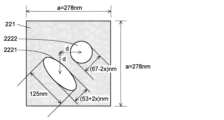
- the parameters for determining ⁇ 1 and ⁇ 2 used in this design example will be explained with reference to FIG.
- the base material 121 (Si) has a refractive index of 3.4
- the modified refractive index region 222 (air) has a refractive index of 1.
- the center of gravity of the first partial modified refractive index region 2221 and the center of gravity of the second partial modified refractive index region 2222 are separated by a distance d in the x and y directions, respectively.
- Four examples of 0.266a, 0.272a, 0.278a, and 0.284a are prepared for this distance d.
- the length of the major axis of the ellipse of the first partial modified refractive index region 2221 is fixed to 125 nm
- the length of the minor axis is (53+2x) nm
- the first coupling coefficient ⁇ 1 and the second coupling coefficient ⁇ 2 The Hermitian coupling coefficient R ⁇ iI and the non-Hermitian coupling coefficient i ⁇ for obtaining .
- Calculation results are shown in FIG.
- the calculation result of the value ⁇ representing the imaginary part (the real part is 0) of the non-Hermitian coupling coefficient is the distance d between the centers of gravity, the short axis of the ellipse of the first partial modified refractive index region 2221, and the It was almost the same value (approximately 87 cm -1 ), almost independent of 2x, which is the value that determines the diameter.
- 16 data points excluding the two indicated by dashed arrows indicate the calculation results of the above 16 examples.
- R, I, the latter shows R, I when the intensity of the reflected light is 1.
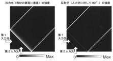
- output light is output from the diffraction grating 22 in a direction perpendicular to the base material 221 (FIG. 17). left figure), whereas almost no reflected light is generated (right figure).
- the diffraction grating coupler 20 of the second embodiment makes the light input from the first input port 231 and the second input port 232 perpendicular to the base material 221. It can be seen that the output can be efficiently performed in the direction of
- the second embodiment can also be used as an optical amplifier by providing an optical amplification layer (active layer) on the surface or inside of the diffraction grating 22 .
- the diffraction grating coupler according to Section 1 is A plate-shaped base material, and dots periodically arranged two-dimensionally or one-dimensionally on the base material, or line-shaped bases periodically arranged one-dimensionally on the base material
- the modified refractive index region has an absolute value of a first coupling coefficient, which is an index indicating the intensity of reflection of light traveling in a first direction parallel to the base material in a second direction different from the first direction by 180°.
- of the second coupling coefficient which is an index indicating the intensity at which the light traveling in the second direction is reflected in the first direction, to
- the diffraction grating coupler according to the second term is the diffraction grating coupler according to the first term, wherein each of the modified refractive index regions includes a first partial modified refractive index region and the first partial modified refractive index region.
- the refractive index region is a pair of a second partial modified refractive index region that differs in either or both of shape and area.
- the diffraction grating coupler according to the third term is the diffraction grating coupler according to the first or second term, wherein the input light is applied to the end of the base material on the origin side in the first direction.
- An optical input section for input is provided.
- the diffraction grating coupler according to item 4 is the diffraction grating coupler according to any one of items 1 to 3, further comprising: A light amplification layer for amplifying light of a predetermined wavelength is provided on the surface of the material.
Landscapes
- Physics & Mathematics (AREA)
- General Physics & Mathematics (AREA)
- Optics & Photonics (AREA)
- Condensed Matter Physics & Semiconductors (AREA)
- Electromagnetism (AREA)
- Engineering & Computer Science (AREA)
- Microelectronics & Electronic Packaging (AREA)
- Optical Integrated Circuits (AREA)
Priority Applications (2)
| Application Number | Priority Date | Filing Date | Title |
|---|---|---|---|
| JP2023543744A JP7803564B2 (ja) | 2021-08-24 | 2022-07-12 | 回折格子結合器 |
| US18/685,340 US20240369748A1 (en) | 2021-08-24 | 2022-07-12 | Grating coupler |
Applications Claiming Priority (2)
| Application Number | Priority Date | Filing Date | Title |
|---|---|---|---|
| JP2021-136313 | 2021-08-24 | ||
| JP2021136313 | 2021-08-24 |
Publications (1)
| Publication Number | Publication Date |
|---|---|
| WO2023026712A1 true WO2023026712A1 (ja) | 2023-03-02 |
Family
ID=85322745
Family Applications (1)
| Application Number | Title | Priority Date | Filing Date |
|---|---|---|---|
| PCT/JP2022/027386 Ceased WO2023026712A1 (ja) | 2021-08-24 | 2022-07-12 | 回折格子結合器 |
Country Status (3)
| Country | Link |
|---|---|
| US (1) | US20240369748A1 (https=) |
| JP (1) | JP7803564B2 (https=) |
| WO (1) | WO2023026712A1 (https=) |
Cited By (1)
| Publication number | Priority date | Publication date | Assignee | Title |
|---|---|---|---|---|
| WO2025047600A1 (ja) | 2023-08-30 | 2025-03-06 | 国立大学法人京都大学 | 回折格子結合器 |
Citations (4)
| Publication number | Priority date | Publication date | Assignee | Title |
|---|---|---|---|---|
| JP2009058553A (ja) * | 2007-08-30 | 2009-03-19 | Univ Of Tsukuba | ブレーズ型光結合素子及びそれを使用した光機能素子 |
| US20150260913A1 (en) * | 2012-08-17 | 2015-09-17 | Oracle International Corporation | Grating coupler for inter-chip optical coupling |
| US20170363931A1 (en) * | 2016-06-17 | 2017-12-21 | Raymond C. Rumpf | Spatially variant photonic crystal apparatus, methods, and applications |
| WO2018155535A1 (ja) * | 2017-02-24 | 2018-08-30 | 国立大学法人横浜国立大学 | 光偏向デバイス |
-
2022
- 2022-07-12 US US18/685,340 patent/US20240369748A1/en active Pending
- 2022-07-12 WO PCT/JP2022/027386 patent/WO2023026712A1/ja not_active Ceased
- 2022-07-12 JP JP2023543744A patent/JP7803564B2/ja active Active
Patent Citations (4)
| Publication number | Priority date | Publication date | Assignee | Title |
|---|---|---|---|---|
| JP2009058553A (ja) * | 2007-08-30 | 2009-03-19 | Univ Of Tsukuba | ブレーズ型光結合素子及びそれを使用した光機能素子 |
| US20150260913A1 (en) * | 2012-08-17 | 2015-09-17 | Oracle International Corporation | Grating coupler for inter-chip optical coupling |
| US20170363931A1 (en) * | 2016-06-17 | 2017-12-21 | Raymond C. Rumpf | Spatially variant photonic crystal apparatus, methods, and applications |
| WO2018155535A1 (ja) * | 2017-02-24 | 2018-08-30 | 国立大学法人横浜国立大学 | 光偏向デバイス |
Non-Patent Citations (4)
| Title |
|---|
| GELLETA JOHN, H. KITAGAWA, S. NODA: "Coupled-wave analysis for photonic crystal surface-emitting lasers II – Optical loss in photonic crystals with external reflection –", LECTURE PREPRINTS OF THE 63RD JSAP SPRING MEETING, 22 March 2016 (2016-03-22), XP093041139, Retrieved from the Internet <URL:https://confit.atlas.jp/guide/event-img/jsap2016s/20p-P4-2/public/pdf?type=in> [retrieved on 20230421] * |
| LIANG YONG, PENG CHAO, SAKAI KYOSUKE, IWAHASHI SEITA, NODA SUSUMU: "Three-dimensional coupled-wave model for square-lattice photonic crystal lasers with transverse electric polarization: A general approach", PHYSICAL REVIEW B, AMERICAN PHYSICAL SOCIETY, US, vol. 84, no. 19, 1 November 2011 (2011-11-01), US , pages 70, XP093041144, ISSN: 1098-0121, DOI: 10.1103/PhysRevB.84.195119 * |
| MAEKAWA, KYOHEI; NISHIMOTO, M.; YASUDA, D.; ISHIZAKI, K.; KITAMURA, K.; NODA, S.: "20p-P4-4 Fabrication of photonic crystal structures with tilted vacancy -Towards the emission of a circularly polarized beam", 63RD JSAP SPRING MEETING, JAPAN SOCIETY OF APPLIED PHYSICS AND RELATED SOCIETIES; TOKYO; MARCH 19-22, 2016, vol. 63, 29 February 2016 (2016-02-29) - 22 March 2016 (2016-03-22), pages 03, XP009543944, DOI: 10.11470/jsapmeeting.2016.1.0_945 * |
| MIZUTANI AKIO, ETO YOHEI, KIKUTA HISAO: "A grating coupler with a trapezoidal hole array for perfectly vertical light coupling between optical fibers and waveguides", APPLIED PHYSICS EXPRESS, JAPAN SOCIETY OF APPLIED PHYSICS; JP, JP, vol. 10, no. 12, 1 December 2017 (2017-12-01), JP , pages 122501, XP093041143, ISSN: 1882-0778, DOI: 10.7567/APEX.10.122501 * |
Cited By (1)
| Publication number | Priority date | Publication date | Assignee | Title |
|---|---|---|---|---|
| WO2025047600A1 (ja) | 2023-08-30 | 2025-03-06 | 国立大学法人京都大学 | 回折格子結合器 |
Also Published As
| Publication number | Publication date |
|---|---|
| JP7803564B2 (ja) | 2026-01-21 |
| US20240369748A1 (en) | 2024-11-07 |
| JPWO2023026712A1 (https=) | 2023-03-02 |
Similar Documents
| Publication | Publication Date | Title |
|---|---|---|
| US11156789B2 (en) | Surface coupled laser and laser optical interposer | |
| US7006732B2 (en) | Polarization splitting grating couplers | |
| US9377587B2 (en) | Fiber optic coupler array | |
| US10992104B2 (en) | Dual layer grating coupler | |
| US10488596B2 (en) | Optical fiber mounted photonic integrated circuit device | |
| JP6289401B2 (ja) | スポットサイズ変換器 | |
| JP3349950B2 (ja) | 波長分波回路 | |
| US5640474A (en) | Easily manufacturable optical self-imaging waveguide | |
| US20160116680A1 (en) | Light coupling structure and optical device including a grating coupler | |
| JP2000056146A (ja) | 自己導波光回路 | |
| JP6233083B2 (ja) | 光素子 | |
| WO2015111458A1 (ja) | グレーティングカプラ | |
| JP3456166B2 (ja) | フォトニック結晶を用いた光結合素子および光結合方法 | |
| WO2003081305A1 (en) | Two-dimensional photonic crystal point defect interference optical resonator and optical reflector | |
| US6782169B2 (en) | System for efficient coupling to photonic crystal waveguides | |
| JP7803564B2 (ja) | 回折格子結合器 | |
| KR100580658B1 (ko) | 광 결정을 이용한 광 아이솔레이터 | |
| JP2001133647A (ja) | 導波路型高次モードフィルタおよび半導体レーザ | |
| JP2005519319A (ja) | 特に光集積回路で光ビームを曲げるための装置 | |
| US20130343704A1 (en) | Compact mode-size transition using a focusing reflector | |
| JP6530061B2 (ja) | グレーティングカプラ | |
| US11112552B2 (en) | Light-guide sheet and photoelectric conversion device | |
| JP5372682B2 (ja) | 表面効果3次元フォトニック結晶 | |
| US20200379178A1 (en) | Polarization-splitting granting coupler (psgc) integrated optoelectronic or optical device | |
| JPWO2017026005A1 (ja) | 平面導波路型レーザ装置 |
Legal Events
| Date | Code | Title | Description |
|---|---|---|---|
| 121 | Ep: the epo has been informed by wipo that ep was designated in this application |
Ref document number: 22861003 Country of ref document: EP Kind code of ref document: A1 |
|
| WWE | Wipo information: entry into national phase |
Ref document number: 2023543744 Country of ref document: JP |
|
| NENP | Non-entry into the national phase |
Ref country code: DE |
|
| 122 | Ep: pct application non-entry in european phase |
Ref document number: 22861003 Country of ref document: EP Kind code of ref document: A1 |