WO2023026701A1 - 撮像装置、撮像装置の駆動方法、及びプログラム - Google Patents
撮像装置、撮像装置の駆動方法、及びプログラム Download PDFInfo
- Publication number
- WO2023026701A1 WO2023026701A1 PCT/JP2022/027037 JP2022027037W WO2023026701A1 WO 2023026701 A1 WO2023026701 A1 WO 2023026701A1 JP 2022027037 W JP2022027037 W JP 2022027037W WO 2023026701 A1 WO2023026701 A1 WO 2023026701A1
- Authority
- WO
- WIPO (PCT)
- Prior art keywords
- phase difference
- mode
- pixel group
- information
- region
- Prior art date
- Legal status (The legal status is an assumption and is not a legal conclusion. Google has not performed a legal analysis and makes no representation as to the accuracy of the status listed.)
- Ceased
Links
Images




Classifications
-
- H—ELECTRICITY
- H04—ELECTRIC COMMUNICATION TECHNIQUE
- H04N—PICTORIAL COMMUNICATION, e.g. TELEVISION
- H04N25/00—Circuitry of solid-state image sensors [SSIS]; Control thereof
- H04N25/10—Circuitry of solid-state image sensors [SSIS]; Control thereof for transforming different wavelengths into image signals
- H04N25/11—Arrangement of colour filter arrays [CFA]; Filter mosaics
- H04N25/13—Arrangement of colour filter arrays [CFA]; Filter mosaics characterised by the spectral characteristics of the filter elements
- H04N25/134—Arrangement of colour filter arrays [CFA]; Filter mosaics characterised by the spectral characteristics of the filter elements based on three different wavelength filter elements
-
- G—PHYSICS
- G02—OPTICS
- G02B—OPTICAL ELEMENTS, SYSTEMS OR APPARATUS
- G02B7/00—Mountings, adjusting means, or light-tight connections, for optical elements
- G02B7/28—Systems for automatic generation of focusing signals
-
- G—PHYSICS
- G02—OPTICS
- G02B—OPTICAL ELEMENTS, SYSTEMS OR APPARATUS
- G02B7/00—Mountings, adjusting means, or light-tight connections, for optical elements
- G02B7/28—Systems for automatic generation of focusing signals
- G02B7/34—Systems for automatic generation of focusing signals using different areas in a pupil plane
-
- G—PHYSICS
- G03—PHOTOGRAPHY; CINEMATOGRAPHY; ANALOGOUS TECHNIQUES USING WAVES OTHER THAN OPTICAL WAVES; ELECTROGRAPHY; HOLOGRAPHY
- G03B—APPARATUS OR ARRANGEMENTS FOR TAKING PHOTOGRAPHS OR FOR PROJECTING OR VIEWING THEM; APPARATUS OR ARRANGEMENTS EMPLOYING ANALOGOUS TECHNIQUES USING WAVES OTHER THAN OPTICAL WAVES; ACCESSORIES THEREFOR
- G03B13/00—Viewfinders; Focusing aids for cameras; Means for focusing for cameras; Autofocus systems for cameras
- G03B13/32—Means for focusing
- G03B13/34—Power focusing
- G03B13/36—Autofocus systems
-
- H—ELECTRICITY
- H04—ELECTRIC COMMUNICATION TECHNIQUE
- H04N—PICTORIAL COMMUNICATION, e.g. TELEVISION
- H04N25/00—Circuitry of solid-state image sensors [SSIS]; Control thereof
- H04N25/40—Extracting pixel data from image sensors by controlling scanning circuits, e.g. by modifying the number of pixels sampled or to be sampled
- H04N25/42—Extracting pixel data from image sensors by controlling scanning circuits, e.g. by modifying the number of pixels sampled or to be sampled by switching between different modes of operation using different resolutions or aspect ratios, e.g. switching between interlaced and non-interlaced mode
-
- H—ELECTRICITY
- H04—ELECTRIC COMMUNICATION TECHNIQUE
- H04N—PICTORIAL COMMUNICATION, e.g. TELEVISION
- H04N25/00—Circuitry of solid-state image sensors [SSIS]; Control thereof
- H04N25/70—SSIS architectures; Circuits associated therewith
- H04N25/703—SSIS architectures incorporating pixels for producing signals other than image signals
- H04N25/704—Pixels specially adapted for focusing, e.g. phase difference pixel sets
Definitions
- the technology of the present disclosure relates to an imaging device, an imaging device driving method, and a program.
- Japanese Patent Application Laid-Open No. 2002-200000 describes focus detection means for detecting a defocus amount for each of a plurality of predetermined focus detection areas from an image signal output from an imaging device, and creates distance distribution information based on the defocus amount.
- focus adjustment means for performing focus adjustment based on the distance distribution information and the defocus amount; and when the distance distribution information is created by the creation means, the diaphragm included in the imaging optical system is determined in advance.
- the aperture is set to a second depth of field that is shallower than the first depth of field.
- a control means for performing control to set a second aperture value, which is the depth of field, for photographing.
- Patent Document 2 when a microcomputer executes a shift calculation for obtaining ranging data in a plurality of ranging areas set within the imaging area of a ranging sensor, a ranging area other than the center of the imaging area is used.
- a multi-point distance measuring device is disclosed in which the number of shifts for shift calculations for the distance measurement area set in the center of the photographing area is set to be smaller than the number of shifts for shift calculations for the distance measurement area set in the center of the photographing area, thereby shortening the time required for distance measurement calculations.
- Patent Document 3 discloses an imaging unit that captures parallax images, a first generation unit that generates a viewing image from the parallax images captured by the imaging unit, and a first generation unit that generates a distance image from the parallax images captured by the imaging unit.
- a measurement unit that obtains measurement information about a subject in a viewing image using a distance image; assists in setting the shooting conditions of the image capturing unit based on the viewing image or the viewing image parallax image in order to capture the parallax image for the distance image to be used for the generation of the distance image by the second generation unit, or
- An electronic device includes an assist unit that assists in setting shooting conditions of an imaging unit based on a distance image or a parallax image for a distance image in order to shoot in reverse order.
- An embodiment according to the technology of the present disclosure provides an imaging device, a method for driving the imaging device, and a program that enable high-speed acquisition of distance information.
- an imaging device of the present disclosure includes an image sensor having a phase difference pixel group including a first phase difference pixel group and a second phase difference pixel group, and at least one processor. And, the processor is in a mode related to focusing on the subject, and the first phase difference information obtained from the first phase difference pixel group in the first region and the second phase difference pixel group in the first region
- a first mode for obtaining focus information of a first region is executed by performing a first shift operation on the obtained second phase difference information, and the first mode is a mode different from the first mode and is larger than the first region.
- performing a second mode of obtaining distance information of a second region by performing a second shift calculation on first phase difference information and second phase difference information corresponding to the two regions; is smaller than the shift range in the first shift operation.
- the second area preferably includes the area of the subject that is in focus.
- the information amount of the first phase difference information and the second phase difference information is larger than that in the first shift calculation.
- the processor obtains first phase difference information and second phase difference information by encoding signals obtained from the first phase difference pixel group and the second phase difference pixel group. preferably configured.
- the processor converts signals obtained from the first phase difference pixel group into first phase difference information by a local binary encoding method, and converts signals obtained from the second phase difference pixel group into local binary code. conversion to the second phase difference information by the conversion method, and as a second shift operation, a bit operation is performed on the first phase difference information and the second phase difference information, so that a plurality of pixels represented by the result of the bit operation are It is preferably configured to obtain distance information including:
- the processor is preferably configured to generate a phase contrast image based on signals obtained from the first phase contrast pixel group and the second phase contrast pixel group in the second mode.
- the processor In the second mode, the processor generates the first phase difference information and the second phase difference information based on the signals obtained from the first phase difference pixel group and the second phase difference pixel group, and the result of the bit operation is Based on this, it is preferably arranged to generate a distance map in which the distances are visually identifiable for the user.
- the processor is preferably configured to control the second shift operation based on the image structure of the object in the second mode.
- the image structure of the subject is preferably the outline of the subject.
- a method of driving an imaging device of the present disclosure is a method of driving an imaging device including an image sensor having a phase difference pixel group including a first phase difference pixel group and a second phase difference pixel group, and relates to focusing on a subject. mode, in which the first phase difference information obtained from the first phase difference pixel group in the first region and the second phase difference information obtained from the second phase difference pixel group in the first region are subjected to the first shift calculation By doing so, a first mode for acquiring focusing information of the first region is executed, which is a mode different from the first mode, and the first phase difference information corresponding to the second region larger than the first region and the second phase difference information corresponding to the second region.
- a second mode of acquiring distance information of a second region is executed by performing a second shift operation on the phase difference information, and the shift range in the second shift operation is smaller than the shift range in the first shift operation.
- a program of the present disclosure is a program for operating an imaging device including an image sensor having a phase difference pixel group including a first phase difference pixel group and a second phase difference pixel group, and is a mode related to focusing on a subject.
- the first phase difference information obtained from the first phase difference pixel group in the first region and the second phase difference information obtained from the second phase difference pixel group in the first region by performing a first shift operation The imaging device is caused to execute a first mode for acquiring focus information of a first region, and the first phase difference information and the second phase difference information corresponding to a second region, which is a mode different from the first mode and which is larger than the first region, are operated.
- the imaging device executes a second mode for obtaining distance information of the second region by performing a second shift operation on the phase difference information, and the shift range in the second shift operation is the shift range in the first shift operation. Less than shift range.
- FIG. 7 is a diagram conceptually showing an example of focus information acquisition processing
- FIG. 7 is a diagram conceptually showing an example of distance information acquisition processing
- FIG. 2 is a diagram conceptually showing an example of encoding processing by the LBE method
- FIG. 4 is a diagram conceptually showing an example of sub-pixel interpolation processing;
- FIG. 4 is a diagram conceptually showing an example of color allocation processing; It is a figure which shows an example of a distance map typically.
- 4 is a flow chart showing an example of the operation of the imaging device; 6 is a flowchart showing an example of distance information acquisition processing;
- IC is an abbreviation for “Integrated Circuit”.
- CPU is an abbreviation for "Central Processing Unit”.
- ROM is an abbreviation for “Read Only Memory”.
- RAM is an abbreviation for “Random Access Memory”.
- CMOS is an abbreviation for "Complementary Metal Oxide Semiconductor.”
- FPGA is an abbreviation for "Field Programmable Gate Array”.
- PLD is an abbreviation for "Programmable Logic Device”.
- ASIC is an abbreviation for "Application Specific Integrated Circuit”.
- OPF is an abbreviation for "Optical View Finder”.
- EVF is an abbreviation for "Electronic View Finder”.
- JPEG is an abbreviation for "Joint Photographic Experts Group”.
- AF is an abbreviation for "Auto Focus”.
- MF is an abbreviation for "Manual Focus”.
- LBE is an abbreviation for "Local Binary Encoding”.
- LBP is an abbreviation for "Local Binary Pattern”.
- the technology of the present disclosure will be described by taking a lens-interchangeable digital camera as an example.
- the technique of the present disclosure is not limited to interchangeable-lens type digital cameras, and can be applied to lens-integrated digital cameras.
- FIG. 1 shows an example of the configuration of the imaging device 10.
- the imaging device 10 is a lens-interchangeable digital camera.
- the imaging device 10 is composed of a body 11 and an imaging lens 12 replaceably attached to the body 11 .
- the imaging lens 12 is attached to the front side of the main body 11 via a camera side mount 11A and a lens side mount 12A.
- the main body 11 is provided with an operation unit 13 including dials, a release button, and the like.
- the operation modes of the imaging device 10 include, for example, a still image imaging mode, a moving image imaging mode, and an image display mode.
- the operation unit 13 is operated by the user when setting the operation mode. Further, the operation unit 13 is operated by the user when starting execution of still image capturing or moving image capturing.
- the operation modes include an autofocus (AF) mode and a manual focus (MF) mode.
- AF mode a focus information acquisition mode for acquiring focus information of a subject is executed.
- MF mode a distance information acquisition mode for acquiring distance information of a subject is executed.
- MF mode the user can perform focus adjustment while referring to distance information.
- Manual focusing is performed, for example, by operating a focus ring (not shown) provided on the imaging lens 12 .
- the focus information acquisition mode is an example of the "first mode” according to the present disclosure.
- the distance information acquisition mode is an example of the "second mode” according to the present disclosure.
- AF mode and MF mode are selected by the operation of the operation unit 13 by the user.
- the instruction to select the AF mode is an example of the "first instruction” according to the present disclosure.
- An instruction to select the MF mode is an example of a "second instruction” according to the present disclosure.
- the main body 11 is provided with a finder 14 .
- the finder 14 is a hybrid finder (registered trademark).
- a hybrid viewfinder is, for example, a viewfinder that selectively uses an optical viewfinder (hereinafter referred to as "OVF") and an electronic viewfinder (hereinafter referred to as "EVF").
- OVF optical viewfinder
- EMF electronic viewfinder
- a user can observe an optical image or a live view image of a subject projected through the viewfinder 14 through a viewfinder eyepiece (not shown).
- a display 15 is provided on the back side of the main body 11 .
- the display 15 displays an image based on an image signal obtained by imaging, various menu screens, and the like.
- the body 11 and the imaging lens 12 are electrically connected by contact between an electrical contact 11B provided on the camera side mount 11A and an electrical contact 12B provided on the lens side mount 12A.
- the imaging lens 12 includes an objective lens 30, a focus lens 31, a rear end lens 32, and an aperture 33. Each member is arranged along the optical axis A of the imaging lens 12 in the order of the objective lens 30, the diaphragm 33, the focus lens 31, and the rear end lens 32 from the objective side.
- the objective lens 30, focus lens 31, and rear end lens 32 constitute an imaging optical system.
- the type, number, and order of arrangement of lenses that constitute the imaging optical system are not limited to the example shown in FIG.
- the imaging lens 12 also has a lens drive control section 34 .
- the lens drive control unit 34 is composed of, for example, a CPU, a RAM, a ROM, and the like.
- the lens drive control section 34 is electrically connected to the processor 40 in the main body 11 via the electrical contacts 12B and 11B.
- the lens drive control unit 34 drives the focus lens 31 and the diaphragm 33 based on control signals sent from the processor 40 .
- the lens drive control unit 34 performs drive control of the focus lens 31 based on a control signal for focus control transmitted from the processor 40 in order to adjust the focus position of the imaging lens 12 .
- the processor 40 performs phase-contrast focusing.
- the diaphragm 33 has an aperture whose aperture diameter is variable around the optical axis A.
- the lens drive control unit 34 performs drive control of the diaphragm 33 based on the control signal for diaphragm adjustment transmitted from the processor 40.
- an imaging sensor 20 a processor 40, and a memory 42 are provided inside the main body 11.
- the operations of the imaging sensor 20 , the memory 42 , the operation unit 13 , the viewfinder 14 and the display 15 are controlled by the processor 40 .
- the processor 40 is composed of, for example, a CPU, RAM, and ROM. In this case, processor 40 executes various processes based on program 43 stored in memory 42 . Note that the processor 40 may be configured by an assembly of a plurality of IC chips.
- the imaging sensor 20 is, for example, a CMOS image sensor.
- the imaging sensor 20 is arranged such that the optical axis A is orthogonal to the light receiving surface 20A and the optical axis A is positioned at the center of the light receiving surface 20A.
- Light (subject image) that has passed through the imaging lens 12 is incident on the light receiving surface 20A.
- a plurality of pixels that generate image signals by performing photoelectric conversion are formed on the light receiving surface 20A.
- the imaging sensor 20 photoelectrically converts light incident on each pixel to generate and output an image signal.
- the imaging sensor 20 is an example of an “image sensor” according to the technology of the present disclosure.
- a color filter array of Bayer arrangement is arranged on the light receiving surface of the imaging sensor 20, and one of R (red), G (green), and B (blue) color filters is arranged opposite to each pixel. It is Some of the plurality of pixels arranged on the light receiving surface of the image sensor 20 are phase difference pixels for acquiring parallax information. The phase difference pixels are not provided with color filters. A pixel provided with a color filter is hereinafter referred to as a normal pixel.
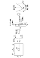
- FIG. 2 shows an example of the configuration of the imaging pixel N.
- FIG. FIG. 3 shows an example of the configuration of the phase difference pixels P1 and P2.
- the phase difference pixels P1 and P2 each receive one of the beams split in the X direction around the principal ray.
- the imaging pixel N includes a photodiode PD as a photoelectric conversion element, a color filter CF, and a microlens ML.
- a color filter CF is arranged between the photodiode PD and the microlens ML.
- the color filter CF is a filter that transmits light of any one of R, G, and B colors.
- the microlens ML converges the luminous flux LF incident from the exit pupil EP of the imaging lens 12 on substantially the center of the photodiode PD via the color filter CF.
- the phase difference pixels P1 and P2 each include a photodiode PD, a light shielding layer SF, and a microlens ML.
- the microlens ML converges the light flux LF incident from the exit pupil EP of the image pickup lens 12 on substantially the center of the photodiode PD.
- the light shielding layer SF is formed of a metal film or the like, and is arranged between the photodiode PD and the microlens ML.
- the light shielding layer SF shields part of the light flux LF incident on the photodiode PD via the microlens ML.
- the light shielding layer SF shields the negative side in the X direction with the center of the photodiode PD as a reference. That is, in the phase difference pixel P1, the light shielding layer SF allows the light flux LF from the negative exit pupil EP1 to enter the photodiode PD and blocks the light flux LF from the positive exit pupil EP2 in the X direction.
- the light shielding layer SF shields the positive side in the X direction with the center of the photodiode PD as a reference. That is, in the phase difference pixel P2, the light shielding layer SF allows the light flux LF from the positive exit pupil EP2 to enter the photodiode PD and blocks the light flux LF from the negative exit pupil EP1 in the X direction.
- phase difference pixel P1 and the phase difference pixel P2 are different from each other in the light shielding position.
- the plurality of phase difference pixels P1 is an example of the "first phase difference pixel group" according to the technology of the present disclosure.
- the plurality of phase difference pixels P2 is an example of the "second phase difference pixel group” according to the technology of the present disclosure.
- FIG. 4 shows an example of the pixel array of the imaging sensor 20.
- FIG. "R” in FIG. 4 represents the imaging pixel N provided with the R color filter CF.
- “G” represents an imaging pixel N provided with a G color filter CF.
- “B” represents an imaging pixel N provided with a B color filter CF. Note that the color arrangement of the color filters CF is not limited to the Bayer arrangement, and may be another color arrangement.
- Rows RL including phase difference pixels P1 and P2 are arranged every 10 pixels in the Y direction.
- a pair of phase difference pixels P1 and P2 and one imaging pixel N are repeatedly arranged in the Y direction.
- the arrangement pattern of the phase difference pixels P1 and P2 is not limited to the example shown in FIG. For example, it may be a pattern in which a plurality of phase difference pixels are arranged in one microlens ML, as shown in FIG. 5 attached to JP-A-2018-56703.
- FIG. 5 shows an example of the functional configuration of the processor 40.
- the processor 40 implements various functional units by executing processes according to programs 43 stored in the memory 42 .
- the processor 40 implements a main control unit 50, an imaging control unit 51, an image processing unit 52, a focus information acquisition unit 53, and a distance information acquisition unit .
- the main control unit 50 comprehensively controls the operation of the imaging device 10 based on instruction signals input from the operation unit 13 .
- the imaging control unit 51 controls the imaging sensor 20 to perform an imaging process for causing the imaging sensor 20 to perform an imaging operation.
- the imaging control unit 51 drives the imaging sensor 20 in still image imaging mode or moving image imaging mode.
- the image processing unit 52 performs various image processing on the RAW image RD output from the imaging sensor 20 to generate a captured image 56 in a predetermined file format (eg, JPEG format, etc.).
- a captured image 56 output from the image processing unit 52 is recorded in the memory 42, for example.
- the captured image 56 is output to the display 15 and displayed on the display 15 .
- the captured image 56 is an image generated based on the signals output from the imaging pixels N. As shown in FIG.
- the user can select between the still image capturing mode and the moving image capturing mode using the operation unit 13 .
- the user can select AF mode or MF mode by operating the operation unit 13 .
- the main control section 50 controls the position of the focus lens 31 based on the focus information acquired by the focus information acquisition section 53 .
- the main control section 50 causes the display 15 to display the distance information acquired by the distance information acquisition section 54 together with the captured image 56 .
- the focus information acquisition unit 53 of the RAW image RD output from the imaging sensor 20, based on the signals output from the phase difference pixels P1 and P2 (see FIG. 4) in the AF area 60 (see FIG. 6) In-focus information is acquired by performing the first shift calculation. Acquiring focus information corresponds to detecting the position of the focus lens 31 at which the subject is in focus.
- the AF area is an area of the imaging sensor 20 that captures an image of a subject to be focused determined by the user or the imaging device 10 .
- the distance information acquisition unit 54 performs a second shift calculation based on the signals output from the phase difference pixels P1 and P2 (see FIG. 4) in the imaging area 62 in the RAW image RD output from the imaging sensor 20.
- the distance information is obtained by Note that the imaging area is the imaging area of the imaging sensor 20 and is larger than the AF area.
- the AF area is an example of the "first area” according to the technology of the present disclosure.
- the imaging area is an example of the "second area” according to the technology of the present disclosure.
- FIG. 6 conceptually shows an example of focus information acquisition processing by the focus information acquisition unit 53 .
- the focus information acquisition unit 53 acquires first phase difference information D1 from a plurality of phase difference pixels P1 included in the AF area 60 based on the RAW image RD.
- Second phase difference information D2 is obtained from the plurality of phase difference pixels P2.
- the first phase difference information D1 is composed of pixel signals output from the phase difference pixels P1.
- the second phase difference information D2 is composed of pixel signals output from the phase difference pixels P2.
- the angle of view of the AF area 60 is about 10% of the angle of view of the imaging area 62 .
- the AF area 60 is set by a user's operation using the operation unit 13, for example.
- the AF area 60 includes approximately 200 phase difference pixels P1 and P2 in the X direction.
- the focus information acquisition unit 53 After correcting the sensitivity ratio between the first phase difference information D1 and the second phase difference information D2, the focus information acquisition unit 53 performs the first shift calculation.
- the focus information acquisition unit 53 fixes the first phase difference information D1 and shifts the second phase difference information D2 by one pixel in the X direction while shifting the first phase difference information D1 and the second A difference sum of squares is calculated by performing a correlation calculation with the phase difference information D2.
- the focus information acquisition unit 53 calculates one sum of squared differences each time the second phase difference information D2 is shifted by one pixel.
- the shift range in which the focus information acquisition unit 53 shifts the second phase difference information D2 in the first shift calculation is, for example, the range of ⁇ 50 ⁇ X ⁇ 50.
- ⁇ X represents the amount of shift in the X direction.
- the focus information acquisition unit 53 acquires the shift amount ⁇ that minimizes the sum of squared differences (that is, maximizes the correlation value) in the shift range ( ⁇ 50 ⁇ X ⁇ 50) as focus information.
- the shift amount ⁇ represents the defocus amount.
- the main control unit 50 moves the focus lens 31 based on the shift amount ⁇ as focus information.
- FIG. 7 conceptually shows an example of distance information acquisition processing by the distance information acquisition unit 54.
- the distance information acquisition unit 54 acquires the first signal S1 from the plurality of phase difference pixels P1 included in the imaging area 62 based on the RAW image RD, and the plurality of positions included in the imaging area 62.
- a second signal S2 is obtained from the phase difference pixel P2.
- the first signal S1 is composed of the pixel signal output from the phase difference pixel P1.
- the second signal S2 is composed of the pixel signal output from the phase difference pixel P2.
- the imaging area 62 includes about 2000 phase difference pixels P1 and 2000 phase difference pixels P2 in the X direction.
- the distance information acquisition unit 54 acquires the first phase difference information D1 and the second phase difference information D2 by encoding the first signal S1 and the second signal S2.
- the distance information acquisition unit 54 performs encoding using a local binary encoding (LBE) method.
- LBE local binary encoding
- the distance information acquisition unit 54 converts the first signal S1 into the first phase difference information D1 by the LBE method, and converts the second signal S2 into the second phase difference information D2 by the LBE method.
- the LBE method is a method of converting phase difference information of each pixel or each pixel group into binary information according to a predetermined standard.
- each pixel of the first phase difference information D1 and the second phase difference information D2 is represented by a binary local binary pattern (hereinafter referred to as LBP) encoded by the LBE method.
- LBP binary local binary pattern
- the distance information acquisition unit 54 performs a second shift calculation using the first phase difference information D1 and the second phase difference information D2.
- the distance information acquisition unit 54 fixes the first phase difference information D1, shifts the second phase difference information D2 by one pixel in the X direction, and A difference sum of squares is calculated by performing a correlation calculation with the phase difference information D2.
- the shift range in which the distance information acquisition unit 54 shifts the second phase difference information D2 in the second shift calculation is, for example, the range of ⁇ 2 ⁇ X ⁇ 2.
- ⁇ X represents the amount of shift in the X direction. That is, the shift range in the second shift calculation is smaller than the shift range in the first shift calculation. This is because the second shift calculation targets the phase difference pixels P1 and P2 in the entire imaging area, and the amount of information of the first phase difference information D1 and the second phase difference information D2 to be used is greater than that of the first shift calculation. Because there are many. In the second shift operation, the processing speed is increased by narrowing the shift range.
- the distance information acquisition unit 54 calculates the sum of squared differences by performing a binary operation.
- the distance information acquisition unit 54 performs a binary operation on LBPs included in corresponding pixels of the first phase difference information D1 and the second phase difference information D2.
- the distance information acquisition unit 54 generates a difference map 70 by performing a binary operation each time the second phase difference information D2 is shifted by one pixel.
- Each pixel of the difference map 70 is represented by the result of binary computation.
- the distance information acquisition unit 54 generates a distance map 72 by performing processing such as sub-pixel interpolation based on the plurality of difference maps 70 .
- the main controller 50 causes the display 15 to display the distance map 72 .
- FIG. 8 conceptually shows an example of encoding processing by the LBE method.
- an extraction region 74 is set in the first signal S1, and a plurality of pixel values are obtained from the set extraction region 74.
- the pixel value is the value of the pixel signal output from the phase difference pixel P1.
- the extraction area 74 is an area including 9 pixels arranged in the X direction. Note that the size and shape of the extraction region 74 can be changed as appropriate.
- the distance information acquisition unit 54 sets the central pixel of the extraction region 74 as the pixel of interest PI, and sets the pixel value of the pixel of interest PI as the threshold. Next, the distance information acquisition unit 54 compares the value of the peripheral pixel with a threshold value, and binarizes the value as "1" if it is equal to or greater than the threshold value, and as "0" if it is less than the threshold value. Next, the distance information acquiring unit 54 converts the binarized values of the eight peripheral pixels into 8-bit data to obtain LBP. Then, the distance information acquisition unit 54 replaces the value of the pixel of interest PI with LBP.
- the distance information acquisition unit 54 calculates the LBP while changing the extraction region 74 pixel by pixel, and replaces the value of the target pixel PI with the calculated LBP to generate the first phase difference information D1.
- the encoding process for generating the second phase difference information D2 is the same as the encoding process for generating the first phase difference information D1, so the description is omitted.
- the first phase difference information D1 and the second phase difference information D2 used in the second shift calculation process are composed of 8-bit LBPs for each pixel.
- the amount of information is greater than that of the phase difference information D1 and the second phase difference information D2.
- FIG. 9 and 10 conceptually show an example of the second shift arithmetic processing.
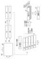
- the distance information acquisition unit 54 reads LBPs from corresponding pixels of the first phase difference information D1 and the second phase difference information D2, respectively, and obtains the exclusive OR (XOR) of the two read LBPs. Further, the distance information acquiring unit 54 performs bit counting on the obtained exclusive OR. Bit counting is to count "1"s included in the exclusive OR represented by a binary number to obtain the number of "1"s. A value obtained by bit counting is hereinafter referred to as a bit count value. In this embodiment, the bit count value is a value in the range of 0-8.
- FIG. 11 conceptually shows an example of sub-pixel interpolation processing.
- the distance information acquisition unit 54 reads out bit count values from corresponding pixels in a plurality of difference maps 70 generated by the second shift calculation process, and converts the read bit count values to the shift amount ⁇ X. to plot. Then, the distance information acquiring unit 54 interpolates the bit count values to obtain an interpolated curve, and obtains a shift amount ⁇ with respect to the minimum value of the interpolated curve.
- the shift amount ⁇ represents the defocus amount, that is, the distance from the in-focus position. The relationship between the shift amount ⁇ and the actual distance depends on the depth of field.
- the shift amount ⁇ is an example of the “bit operation result” according to the technology of the present disclosure.
- FIG. 12 conceptually shows an example of color allocation processing.
- the distance information acquiring unit 54 reads the color corresponding to the shift amount ⁇ obtained by the sub-pixel interpolation process from the color chart 80, and assigns the read color to the pixel for which the shift amount ⁇ is obtained. assign.
- the distance information acquisition unit 54 generates a distance map 72 by performing color allocation processing on all pixels included in the difference map 70 .
- the distance map 72 is distance information in which the shift amount ⁇ , which is the result of the bit operation, is identifiably represented for each pixel (that is, the distance is visually identifiable by the user).
- the distance map 72 is a depth map representing relative distances from the in-focus position. Note that the distance map 72 is an example of "distance information including a plurality of pixels represented by a result of bit operation" according to the technology of the present disclosure.
- the distance information acquisition unit 54 may perform color adjustment after generating the distance map 72 by performing color allocation processing.
- the distance map 72 may be represented by a shift amount ⁇ (that is, a defocus amount) without color allocation processing.
- the distance map 72 is not limited to a depth map representing relative distances from the in-focus position, and may be represented by converting the distances into absolute distances from the imaging sensor 20 .
- FIG. 13 schematically shows an example of the distance map 72.
- objects whose shift amount ⁇ is within the range of ⁇ 1.0 ⁇ 1.0 are colored and displayed on the distance map 72 .
- Objects outside the range ⁇ 1.0 ⁇ 1.0 are represented in black, for example.
- the user can recognize the distance to the object (that is, the defocus amount) based on the color of the object shown on the distance map 72 .
- FIG. 14 is a flowchart showing an example of the operation of the imaging device 10.
- FIG. FIG. 14 shows an example in which the still image capturing mode is selected.
- the main control unit 50 determines whether or not an instruction to select the AF mode or the MF mode (hereinafter referred to as a mode selection instruction) has been given by the user operating the operation unit 13 (step S10).
- a mode selection instruction (step S10: YES)
- the main control unit 50 determines whether or not the selected mode is the AF mode (step S11).
- step S11 When the main control section 50 determines that the selected mode is the AF mode (step S11: YES), the main control section 50 causes the focus information acquisition section 53 to execute the focus information acquisition mode (step S12). In step S12, the focus information acquisition unit 53 performs the focus information acquisition process described above (see FIG. 6). Then, the main control section 50 performs AF control based on the focus information acquired by the focus information acquisition section 53 (step S13).
- step S11 NO
- the main control unit 50 causes the distance information acquisition unit 54 to execute the distance information acquisition mode (step S14).
- step S14 the distance information acquisition unit 54 performs the distance information acquisition process described above (see FIGS. 7 to 13).
- the main control unit 50 causes the display 15 to perform live view display (step S15).
- the main controller 50 causes the display 15 to display the captured image 56 .
- the main controller 50 causes the display 15 to display the distance map 72 .
- step S16 determines whether or not the user has issued a shooting instruction by operating the operation unit 13 (step S16).
- step S16 determines that there is no photographing instruction
- step S16: NO the main control unit 50 determines that there is a shooting instruction
- step S17 the main control unit 50 causes the imaging control unit 51 to perform still image shooting
- the user can accurately focus on a desired subject by manual focusing while checking the distance to the object by referring to the distance map 72 .
- FIG. 15 is a flow chart showing an example of the distance information acquisition process (step S14) shown in FIG.
- the distance information acquisition unit 54 acquires the RAW image RD output from the imaging sensor 20 (step S20).
- the distance information acquisition unit 54 acquires the above-described first signal S1 and second signal S2 from the RAW image RD, and encodes the first signal S1 and second signal S2 by the LBE method (step S21). Thereby, the first phase difference information D1 and the second phase difference information D2 are generated.
- the distance information acquisition unit 54 uses the first phase difference information D1 and the second phase difference information D2 to perform the above-described second shift calculation (step S22).
- the distance information acquisition unit 54 performs the sub-pixel interpolation process described above based on the plurality of difference maps 70 obtained by the second shift calculation (step S23).
- the distance information acquisition unit 54 performs the above-described color allocation process of allocating a color corresponding to the shift amount ⁇ obtained as a result of the sub-pixel interpolation process (step S24). Then, the distance information acquisition unit 54 performs color adjustment on the distance map 72 generated as a result of the color allocation process (step S25).
- the area for acquiring distance information is the entire imaging area 62, which is larger than the AF area 60, which is the area for acquiring focus information by the focus information acquisition process.
- the shift range in the second shift calculation used in the distance information acquisition process is smaller than the shift range in the first shift calculation used in the focus information acquisition process, distance information can be acquired at high speed.
- the first phase difference information D1 and the second phase difference information D2 are generated by encoding the first signal S1 and the second signal S2, so the phase difference pixel P1 and the phase difference pixel P2. Therefore, it is not necessary to perform sensitivity ratio correction on the first phase difference information D1 and the second phase difference information D2.
- the first signal S1 and the second signal S2 are encoded by the LBE method, so each pixel of the first phase difference information D1 and the second phase difference information D2 is multi-bit of LBP. Therefore, correlation calculation can be performed with high accuracy.
- the phase difference image is generated based on the signals of the rows in which the first phase difference pixels P1 and the second phase difference pixels P2 are arranged, and the first phase difference information is based on the generated phase difference image.
- D1 and second phase difference information D2 may be generated.
- the distance information acquisition unit 54 acquires distance information for the entire imaging area 62, but the area from which the distance information is acquired does not have to be the entire imaging area 62.
- the distance information acquisition unit 54 detects an image structure of a subject (for example, contour, characteristic structure of the subject, contrast difference, etc.), and acquires distance information for an area within the detected characteristic image structure. good too. That is, by detecting a characteristic image structure and not performing the second shift operation on regions other than the detected image structure, it is possible to speed up the processing.
- a typical example of a characteristic image structure is the contour of a subject.
- the following various processors can be used as the hardware structure of the control unit, with the processor 40 being an example.
- the above-mentioned various processors include CPUs, which are general-purpose processors that function by executing software (programs), as well as processors such as FPGAs whose circuit configuration can be changed after manufacture.
- FPGAs include dedicated electric circuits, which are processors with circuitry specifically designed to perform specific processing, such as PLDs or ASICs.
- the control unit may be configured with one of these various processors, or a combination of two or more processors of the same type or different types (for example, a combination of multiple FPGAs or a combination of a CPU and an FPGA). may consist of Also, the plurality of control units may be configured by one processor.
- control unit there are multiple possible examples of configuring multiple control units with a single processor.
- first example as typified by computers such as clients and servers, there is a mode in which one or more CPUs and software are combined to form one processor, and this processor functions as a plurality of control units.
- second example is the use of a processor that implements the functions of the entire system including multiple control units with a single IC chip, as typified by System On Chip (SOC).
- SOC System On Chip
- an electric circuit combining circuit elements such as semiconductor elements can be used.
- Imaging Device 11 Main Body 11A Camera Side Mount 11B Electric Contact 12 Imaging Lens 12A Lens Side Mount 12B Electric Contact 13 Operation Unit 14 Viewfinder 15 Display 20 Image Sensor 20A Light Receiving Surface 30 Objective Lens 31 Focus Lens 32 Rear End Lens 34 Lens Drive Control Unit 40 processor 42 memory 43 program 50 main control unit 51 imaging control unit 52 image processing unit 53 focus information acquisition unit 54 distance information acquisition unit 56 captured image 60 AF area 62 imaging area 70 difference map 72 distance map 74 extraction area 80 color chart ⁇ X shift amount ⁇ shift amount A optical axis CF color filter PD photodiode D1 first phase difference information D2 second phase difference information EP exit pupil EP1 first exit pupil EP2 second exit pupil H subject LF luminous flux ML microlens N imaging pixel P1 First phase difference pixel P2 Second phase difference pixel PI Pixel of interest RD RAW image RL Row S1 First signal S2 Second signal SF Light shielding layer
Landscapes
- Engineering & Computer Science (AREA)
- Multimedia (AREA)
- Signal Processing (AREA)
- Physics & Mathematics (AREA)
- General Physics & Mathematics (AREA)
- Optics & Photonics (AREA)
- Spectroscopy & Molecular Physics (AREA)
- Studio Devices (AREA)
- Focusing (AREA)
- Automatic Focus Adjustment (AREA)
Priority Applications (2)
| Application Number | Priority Date | Filing Date | Title |
|---|---|---|---|
| JP2023543737A JPWO2023026701A1 (https=) | 2021-08-25 | 2022-07-08 | |
| US18/437,588 US12587761B2 (en) | 2021-08-25 | 2024-02-09 | Imaging apparatus, drive method of imaging apparatus, and program |
Applications Claiming Priority (2)
| Application Number | Priority Date | Filing Date | Title |
|---|---|---|---|
| JP2021-137513 | 2021-08-25 | ||
| JP2021137513 | 2021-08-25 |
Related Child Applications (1)
| Application Number | Title | Priority Date | Filing Date |
|---|---|---|---|
| US18/437,588 Continuation US12587761B2 (en) | 2021-08-25 | 2024-02-09 | Imaging apparatus, drive method of imaging apparatus, and program |
Publications (1)
| Publication Number | Publication Date |
|---|---|
| WO2023026701A1 true WO2023026701A1 (ja) | 2023-03-02 |
Family
ID=85322733
Family Applications (1)
| Application Number | Title | Priority Date | Filing Date |
|---|---|---|---|
| PCT/JP2022/027037 Ceased WO2023026701A1 (ja) | 2021-08-25 | 2022-07-08 | 撮像装置、撮像装置の駆動方法、及びプログラム |
Country Status (3)
| Country | Link |
|---|---|
| US (1) | US12587761B2 (https=) |
| JP (1) | JPWO2023026701A1 (https=) |
| WO (1) | WO2023026701A1 (https=) |
Citations (5)
| Publication number | Priority date | Publication date | Assignee | Title |
|---|---|---|---|---|
| JPS599610A (ja) * | 1982-07-09 | 1984-01-19 | Hitachi Denshi Ltd | 自動合焦装置 |
| JP2000089098A (ja) * | 1998-09-14 | 2000-03-31 | Olympus Optical Co Ltd | 多点測距装置 |
| JP2016148823A (ja) * | 2015-02-13 | 2016-08-18 | キヤノン株式会社 | 焦点検出装置及びその制御方法、撮像装置、プログラム、並びに記憶媒体 |
| JP2018017876A (ja) * | 2016-07-27 | 2018-02-01 | キヤノン株式会社 | 撮像装置及びその制御方法、及び画像処理装置及び方法 |
| WO2019026923A1 (ja) * | 2017-08-03 | 2019-02-07 | オリンパス株式会社 | 画像処理装置、画像処理方法、画像処理プログラム及び撮像装置 |
Family Cites Families (6)
| Publication number | Priority date | Publication date | Assignee | Title |
|---|---|---|---|---|
| KR102150890B1 (ko) * | 2014-02-21 | 2020-09-02 | 삼성전자주식회사 | 이미지 초점 표시 방법 및 상기 방법이 적용되는 전자장치 |
| JP6866636B2 (ja) * | 2016-12-26 | 2021-04-28 | カシオ計算機株式会社 | 文字編集方法、電子機器、及び、プログラム |
| JP6741881B2 (ja) * | 2017-12-07 | 2020-08-19 | 富士フイルム株式会社 | 画像処理装置、撮像装置、画像処理方法、およびプログラム |
| KR102704135B1 (ko) * | 2019-01-22 | 2024-09-09 | 엘지이노텍 주식회사 | 카메라 장치 및 그의 오토포커싱 방법 |
| JP7584901B2 (ja) | 2019-05-17 | 2024-11-18 | キヤノン株式会社 | 電子機器およびその制御方法 |
| US20250203199A1 (en) * | 2021-12-08 | 2025-06-19 | Nikon Corporation | Imaging control device, imaging device, program, and imaging system |
-
2022
- 2022-07-08 WO PCT/JP2022/027037 patent/WO2023026701A1/ja not_active Ceased
- 2022-07-08 JP JP2023543737A patent/JPWO2023026701A1/ja active Pending
-
2024
- 2024-02-09 US US18/437,588 patent/US12587761B2/en active Active
Patent Citations (5)
| Publication number | Priority date | Publication date | Assignee | Title |
|---|---|---|---|---|
| JPS599610A (ja) * | 1982-07-09 | 1984-01-19 | Hitachi Denshi Ltd | 自動合焦装置 |
| JP2000089098A (ja) * | 1998-09-14 | 2000-03-31 | Olympus Optical Co Ltd | 多点測距装置 |
| JP2016148823A (ja) * | 2015-02-13 | 2016-08-18 | キヤノン株式会社 | 焦点検出装置及びその制御方法、撮像装置、プログラム、並びに記憶媒体 |
| JP2018017876A (ja) * | 2016-07-27 | 2018-02-01 | キヤノン株式会社 | 撮像装置及びその制御方法、及び画像処理装置及び方法 |
| WO2019026923A1 (ja) * | 2017-08-03 | 2019-02-07 | オリンパス株式会社 | 画像処理装置、画像処理方法、画像処理プログラム及び撮像装置 |
Also Published As
| Publication number | Publication date |
|---|---|
| US12587761B2 (en) | 2026-03-24 |
| US20240187753A1 (en) | 2024-06-06 |
| JPWO2023026701A1 (https=) | 2023-03-02 |
Similar Documents
| Publication | Publication Date | Title |
|---|---|---|
| JP5159700B2 (ja) | 光学装置及び焦点検出方法 | |
| JP5388544B2 (ja) | 撮像装置およびそのフォーカス制御方法 | |
| JP6584149B2 (ja) | 撮像装置 | |
| JP6249825B2 (ja) | 撮像装置、その制御方法、および制御プログラム | |
| KR101886059B1 (ko) | 촬상장치 및 그 제어 방법 | |
| JP5947601B2 (ja) | 焦点検出装置、その制御方法および撮像装置 | |
| JP6239857B2 (ja) | 撮像装置およびその制御方法 | |
| US9060119B2 (en) | Image capturing apparatus and control method for image capturing apparatus | |
| JP6381266B2 (ja) | 撮像装置、制御装置、制御方法、プログラム、および、記憶媒体 | |
| CN107147858A (zh) | 图像处理装置及其控制方法 | |
| WO2019202984A1 (ja) | 撮像装置並びに距離計測方法、距離計測プログラム及び記録媒体 | |
| JP6254843B2 (ja) | 画像処理装置およびその制御方法 | |
| JP2015194736A (ja) | 撮像装置およびその制御方法 | |
| JP2017032646A (ja) | 撮像装置及びその制御方法 | |
| US20240214677A1 (en) | Detection method, imaging apparatus, and program | |
| JP2015210285A (ja) | 撮像装置及びその制御方法、プログラム、記憶媒体 | |
| JP7309383B2 (ja) | 撮像装置 | |
| WO2023026701A1 (ja) | 撮像装置、撮像装置の駆動方法、及びプログラム | |
| JP2017188633A (ja) | 撮像素子及び撮像装置 | |
| JP6639326B2 (ja) | 制御装置、撮像装置、制御方法、プログラム、および、記憶媒体 | |
| CN114518641B (zh) | 摄像设备、镜头设备及其控制方法和存储介质 | |
| JP2015145970A (ja) | 撮像装置及びその制御方法、プログラム、記憶媒体 | |
| JP2009047735A (ja) | 撮像装置及び画像処理プログラム | |
| US20240187732A1 (en) | Imaging device, method of driving imaging device, and program | |
| JP6765829B2 (ja) | 画像処理装置、画像処理装置の制御方法、撮像装置 |
Legal Events
| Date | Code | Title | Description |
|---|---|---|---|
| 121 | Ep: the epo has been informed by wipo that ep was designated in this application |
Ref document number: 22860992 Country of ref document: EP Kind code of ref document: A1 |
|
| WWE | Wipo information: entry into national phase |
Ref document number: 2023543737 Country of ref document: JP |
|
| NENP | Non-entry into the national phase |
Ref country code: DE |
|
| 122 | Ep: pct application non-entry in european phase |
Ref document number: 22860992 Country of ref document: EP Kind code of ref document: A1 |