WO2022270352A1 - 回路装置 - Google Patents
回路装置 Download PDFInfo
- Publication number
- WO2022270352A1 WO2022270352A1 PCT/JP2022/023769 JP2022023769W WO2022270352A1 WO 2022270352 A1 WO2022270352 A1 WO 2022270352A1 JP 2022023769 W JP2022023769 W JP 2022023769W WO 2022270352 A1 WO2022270352 A1 WO 2022270352A1
- Authority
- WO
- WIPO (PCT)
- Prior art keywords
- partition plate
- circuit device
- circuit
- groove
- heat sink
- Prior art date
- Legal status (The legal status is an assumption and is not a legal conclusion. Google has not performed a legal analysis and makes no representation as to the accuracy of the status listed.)
- Ceased
Links
Images


Classifications
-
- H—ELECTRICITY
- H05—ELECTRIC TECHNIQUES NOT OTHERWISE PROVIDED FOR
- H05K—PRINTED CIRCUITS; CASINGS OR CONSTRUCTIONAL DETAILS OF ELECTRIC APPARATUS; MANUFACTURE OF ASSEMBLAGES OF ELECTRICAL COMPONENTS
- H05K7/00—Constructional details common to different types of electric apparatus
- H05K7/20—Modifications to facilitate cooling, ventilating, or heating
- H05K7/2039—Modifications to facilitate cooling, ventilating, or heating characterised by the heat transfer by conduction from the heat generating element to a dissipating body
-
- H—ELECTRICITY
- H05—ELECTRIC TECHNIQUES NOT OTHERWISE PROVIDED FOR
- H05K—PRINTED CIRCUITS; CASINGS OR CONSTRUCTIONAL DETAILS OF ELECTRIC APPARATUS; MANUFACTURE OF ASSEMBLAGES OF ELECTRICAL COMPONENTS
- H05K3/00—Apparatus or processes for manufacturing printed circuits
- H05K3/22—Secondary treatment of printed circuits
- H05K3/28—Applying non-metallic protective coatings
- H05K3/284—Applying non-metallic protective coatings for encapsulating mounted components
-
- H—ELECTRICITY
- H01—ELECTRIC ELEMENTS
- H01G—CAPACITORS; CAPACITORS, RECTIFIERS, DETECTORS, SWITCHING DEVICES, LIGHT-SENSITIVE OR TEMPERATURE-SENSITIVE DEVICES OF THE ELECTROLYTIC TYPE
- H01G2/00—Details of capacitors not covered by a single one of groups H01G4/00-H01G11/00
- H01G2/02—Mountings
-
- H—ELECTRICITY
- H01—ELECTRIC ELEMENTS
- H01G—CAPACITORS; CAPACITORS, RECTIFIERS, DETECTORS, SWITCHING DEVICES, LIGHT-SENSITIVE OR TEMPERATURE-SENSITIVE DEVICES OF THE ELECTROLYTIC TYPE
- H01G2/00—Details of capacitors not covered by a single one of groups H01G4/00-H01G11/00
- H01G2/08—Cooling arrangements; Heating arrangements; Ventilating arrangements
-
- H—ELECTRICITY
- H01—ELECTRIC ELEMENTS
- H01G—CAPACITORS; CAPACITORS, RECTIFIERS, DETECTORS, SWITCHING DEVICES, LIGHT-SENSITIVE OR TEMPERATURE-SENSITIVE DEVICES OF THE ELECTROLYTIC TYPE
- H01G4/00—Fixed capacitors; Processes of their manufacture
- H01G4/002—Details
- H01G4/224—Housing; Encapsulation
-
- H—ELECTRICITY
- H01—ELECTRIC ELEMENTS
- H01G—CAPACITORS; CAPACITORS, RECTIFIERS, DETECTORS, SWITCHING DEVICES, LIGHT-SENSITIVE OR TEMPERATURE-SENSITIVE DEVICES OF THE ELECTROLYTIC TYPE
- H01G4/00—Fixed capacitors; Processes of their manufacture
- H01G4/32—Wound capacitors
-
- H—ELECTRICITY
- H01—ELECTRIC ELEMENTS
- H01G—CAPACITORS; CAPACITORS, RECTIFIERS, DETECTORS, SWITCHING DEVICES, LIGHT-SENSITIVE OR TEMPERATURE-SENSITIVE DEVICES OF THE ELECTROLYTIC TYPE
- H01G4/00—Fixed capacitors; Processes of their manufacture
- H01G4/38—Multiple capacitors, i.e. structural combinations of fixed capacitors
-
- H—ELECTRICITY
- H02—GENERATION; CONVERSION OR DISTRIBUTION OF ELECTRIC POWER
- H02M—APPARATUS FOR CONVERSION BETWEEN AC AND AC, BETWEEN AC AND DC, OR BETWEEN DC AND DC, AND FOR USE WITH MAINS OR SIMILAR POWER SUPPLY SYSTEMS; CONVERSION OF DC OR AC INPUT POWER INTO SURGE OUTPUT POWER; CONTROL OR REGULATION THEREOF
- H02M7/00—Conversion of AC power input into DC power output; Conversion of DC power input into AC power output
- H02M7/42—Conversion of DC power input into AC power output without possibility of reversal
- H02M7/44—Conversion of DC power input into AC power output without possibility of reversal by static converters
- H02M7/48—Conversion of DC power input into AC power output without possibility of reversal by static converters using discharge tubes with control electrode or semiconductor devices with control electrode
-
- H—ELECTRICITY
- H05—ELECTRIC TECHNIQUES NOT OTHERWISE PROVIDED FOR
- H05K—PRINTED CIRCUITS; CASINGS OR CONSTRUCTIONAL DETAILS OF ELECTRIC APPARATUS; MANUFACTURE OF ASSEMBLAGES OF ELECTRICAL COMPONENTS
- H05K1/00—Printed circuits
- H05K1/18—Printed circuits structurally associated with non-printed electric components
-
- H—ELECTRICITY
- H05—ELECTRIC TECHNIQUES NOT OTHERWISE PROVIDED FOR
- H05K—PRINTED CIRCUITS; CASINGS OR CONSTRUCTIONAL DETAILS OF ELECTRIC APPARATUS; MANUFACTURE OF ASSEMBLAGES OF ELECTRICAL COMPONENTS
- H05K7/00—Constructional details common to different types of electric apparatus
- H05K7/20—Modifications to facilitate cooling, ventilating, or heating
- H05K7/2029—Modifications to facilitate cooling, ventilating, or heating using a liquid coolant with phase change in electronic enclosures
- H05K7/20336—Heat pipes, e.g. wicks or capillary pumps
-
- H—ELECTRICITY
- H05—ELECTRIC TECHNIQUES NOT OTHERWISE PROVIDED FOR
- H05K—PRINTED CIRCUITS; CASINGS OR CONSTRUCTIONAL DETAILS OF ELECTRIC APPARATUS; MANUFACTURE OF ASSEMBLAGES OF ELECTRICAL COMPONENTS
- H05K7/00—Constructional details common to different types of electric apparatus
- H05K7/20—Modifications to facilitate cooling, ventilating, or heating
- H05K7/2039—Modifications to facilitate cooling, ventilating, or heating characterised by the heat transfer by conduction from the heat generating element to a dissipating body
- H05K7/20436—Inner thermal coupling elements in heat dissipating housings, e.g. protrusions or depressions integrally formed in the housing
- H05K7/20445—Inner thermal coupling elements in heat dissipating housings, e.g. protrusions or depressions integrally formed in the housing the coupling element being an additional piece, e.g. thermal standoff
- H05K7/20463—Filling compound, e.g. potted resin
-
- H—ELECTRICITY
- H05—ELECTRIC TECHNIQUES NOT OTHERWISE PROVIDED FOR
- H05K—PRINTED CIRCUITS; CASINGS OR CONSTRUCTIONAL DETAILS OF ELECTRIC APPARATUS; MANUFACTURE OF ASSEMBLAGES OF ELECTRICAL COMPONENTS
- H05K7/00—Constructional details common to different types of electric apparatus
- H05K7/20—Modifications to facilitate cooling, ventilating, or heating
- H05K7/2039—Modifications to facilitate cooling, ventilating, or heating characterised by the heat transfer by conduction from the heat generating element to a dissipating body
- H05K7/20509—Multiple-component heat spreaders; Multi-component heat-conducting support plates; Multi-component non-closed heat-conducting structures
-
- H—ELECTRICITY
- H05—ELECTRIC TECHNIQUES NOT OTHERWISE PROVIDED FOR
- H05K—PRINTED CIRCUITS; CASINGS OR CONSTRUCTIONAL DETAILS OF ELECTRIC APPARATUS; MANUFACTURE OF ASSEMBLAGES OF ELECTRICAL COMPONENTS
- H05K7/00—Constructional details common to different types of electric apparatus
- H05K7/20—Modifications to facilitate cooling, ventilating, or heating
- H05K7/2039—Modifications to facilitate cooling, ventilating, or heating characterised by the heat transfer by conduction from the heat generating element to a dissipating body
- H05K7/20518—Unevenly distributed heat load, e.g. different sectors at different temperatures, localised cooling, hot spots
-
- H—ELECTRICITY
- H10—SEMICONDUCTOR DEVICES; ELECTRIC SOLID-STATE DEVICES NOT OTHERWISE PROVIDED FOR
- H10W—GENERIC PACKAGES, INTERCONNECTIONS, CONNECTORS OR OTHER CONSTRUCTIONAL DETAILS OF DEVICES COVERED BY CLASS H10
- H10W40/00—Arrangements for thermal protection or thermal control
- H10W40/60—Securing means for detachable heating or cooling arrangements, e.g. clamps
-
- H—ELECTRICITY
- H05—ELECTRIC TECHNIQUES NOT OTHERWISE PROVIDED FOR
- H05K—PRINTED CIRCUITS; CASINGS OR CONSTRUCTIONAL DETAILS OF ELECTRIC APPARATUS; MANUFACTURE OF ASSEMBLAGES OF ELECTRICAL COMPONENTS
- H05K2201/00—Indexing scheme relating to printed circuits covered by H05K1/00
- H05K2201/10—Details of components or other objects attached to or integrated in a printed circuit board
- H05K2201/10007—Types of components
- H05K2201/10015—Non-printed capacitor
Definitions
- the present disclosure relates to circuit devices.
- Patent Document 1 Japanese Patent Application Laid-Open No. 2016-66666 (Patent Document 1) describes a capacitor.
- the capacitor described in Patent Document 1 has a lid, electrode plates, a capacitor element, and a case.
- the lid has a substrate and fins. The fins are arranged on one side of the substrate.
- the electrode plate is arranged on the other side of the substrate.
- the capacitor element is arranged on the electrode plate.
- the case is arranged on the lid so as to cover the electrode plate and the capacitor element.
- the present disclosure has been made in view of the problems of the prior art as described above. More specifically, the present disclosure provides circuit devices with improved heat dissipation performance of circuit components.
- a circuit device of the present disclosure includes a first heat sink having a first upper surface, a plurality of first and second partition plates attached to the first upper surface, a sealing material, a first circuit component, and a printed circuit board. and a wiring board.
- the normal direction of the first upper surface is along the first direction.
- the first partition plate extends in a second direction perpendicular to the first direction.
- the second partition plate extends in a third direction orthogonal to the first direction and the second direction.
- the sealing material fills a space defined by two adjacent first partitions, two adjacent second partitions, and the first upper surface.
- a first circuit component is disposed within the encapsulant and is thermally and mechanically coupled.
- a printed wiring board is arranged on the first partition plate and the second partition plate, and is electrically connected to the first circuit component.
- circuit device of the present disclosure it is possible to improve the heat dissipation performance of circuit components.
- FIG. 2 is a circuit diagram of the circuit device 100;
- FIG. 2 is an exploded perspective view of the circuit device 100;
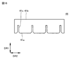
- FIG. 4 is a plan view of a first partition plate 41 included in the circuit device 100;
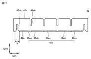
- FIG. 4 is a plan view of a second partition plate 42 included in the circuit device 100;
- FIG. 2 is a cross-sectional view of the circuit device 100;
- FIG. 11 is a perspective view of a circuit device 100 according to a modified example;
- 3 is a perspective view of a first heat sink 30 included in the circuit device 100A;
- FIG. It is a cross-sectional view of the circuit device 100A in the vicinity of the first groove 30d.
- FIG. 10 is a cross-sectional view of the circuit device 100A in the vicinity of the second groove 30e;
- FIG. 4 is a cross-sectional view of the circuit device 100B in the vicinity of the first groove 30d;
- FIG. 10 is a cross-sectional view of the circuit device 100B in the vicinity of the second groove 30e;
- FIG. 4 is a cross-sectional view of the circuit device 100C;
- 3 is a perspective view of a first heat sink 30 included in the circuit device 100D;
- FIG. 4 is a perspective view of the circuit device 100D;
- 4 is a plan view of a first partition plate 43 included in the circuit device 100D;
- FIG. 4 is a plan view of a first partition plate 44 included in the circuit device 100D;
- FIG. 4 is a plan view of a second partition plate 45 included in the circuit device 100D;
- FIG. 4 is a plan view of a second partition plate 46 included in the circuit device 100D;
- FIG. FIG. 4 is a perspective view of the circuit device 100E;
- FIG. 10 is a perspective view of the circuit device 100F;
- FIG. 4 is a cross-sectional view of the circuit device 100F;
- FIG. 4 is a cross-sectional view of the circuit device 100G;
- circuit device 100 A circuit device (hereinafter referred to as “circuit device 100”) according to Embodiment 1 will be described.
- the circuit device 100 is, for example, a power conversion device. Although the circuit device 100 is not limited to a power conversion device, the power conversion device will be described below as an example of the circuit device 100 .
- FIG. 1 is a circuit diagram of a circuit device 100. As shown in FIG. As shown in FIG. 1, the circuit device 100 has a peripheral circuit 110 and a switching circuit 120 .
- the peripheral circuit 110 has a plurality of first circuit components 10.
- the plurality of first circuit components 10 are a capacitor 10a, an inductor 10b, a contactor 10c, a discharging resistor 10d and a charging resistor 10e.
- Capacitor 10a, inductor 10b and contactor 10c are connected in series.
- Inductor 10b is arranged between capacitor 10a and contactor 10c.
- a discharging resistor 10d and a charging resistor 10e are connected in parallel to the capacitor 10a and the contactor 10c, respectively.
- Peripheral circuit 110 is connected to DC supply circuit 130 .
- the switching circuit 120 is, for example, a three-phase inverter circuit.
- the switching circuit 120 has a plurality of second circuit components 20 .
- the plurality of second circuit components 20 are transistors 20a-20f and diodes 20g-20l.
- the drain of the transistor 20a is electrically connected to one electrode of the capacitor 10a.
- the source of transistor 20a is electrically connected to the drain of transistor 20b.
- the source of transistor 20b is electrically connected to the other electrode of capacitor 10a.
- the anode of diode 20g is electrically connected to the source of transistor 20a.
- the cathode of diode 20g is electrically connected to the drain of transistor 20a.
- the anode of diode 20h is electrically connected to the source of transistor 20b.
- the cathode of diode 20h is electrically connected to the drain of transistor 20b.
- the transistor 20c, the transistor 20d, the diode 20i and the diode 20j are connected in the same manner as the transistor 20a, the transistor 20b, the diode 20g and the diode 20h, respectively.
- Transistor 20e, transistor 20f, diode 20k, and diode 20l are connected in the same manner as transistor 20a, transistor 20b, diode 20g, and diode 20h, respectively.
- the gates of transistors 20a-20f are connected to a control circuit.
- the switching circuit 120 is connected to the motor 140.
- Motor 140 is, for example, a three-phase motor.
- Motor 140 has input line 141 , input line 142 , and input line 143 .
- the input line 141 is electrically connected to the source of the transistor 20a and the drain of the transistor 20b.
- the input line 142 is electrically connected to the source of the transistor 20c and the drain of the transistor 20d.
- the input line 143 is electrically connected to the source of the transistor 20e and the drain of the transistor 20f.
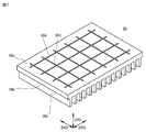
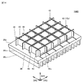
- FIG. 2 is an exploded perspective view of the circuit device 100.
- the circuit device 100 further includes a first heat sink 30, a plurality of first partition plates 41, and a plurality of second partition plates .
- the first heat sink 30 has an upper surface 30a and a lower surface 30b.
- the lower surface 30b is the opposite surface of the upper surface 30a.
- first direction DR1 the direction along the normal line of upper surface 30a
- second direction DR2 a direction orthogonal to the first direction DR1 and the second direction DR2 is defined as a third direction DR3.
- a plurality of fins 30c are formed on the lower surface 30b.
- the fin 30c extends, for example, in the second direction DR2.
- the plurality of fins 30c are spaced apart from each other in the third direction DR3.
- the first heat sink 30 is made of a metal material having excellent thermal conductivity, such as copper (copper alloy) or aluminum (aluminum alloy).
- the first heat sink 30 is formed, for example, by extrusion. Extrusion is performed, for example, along the extending direction (second direction DR2) of the fins 30c.
- the first partition plate 41 is attached to the upper surface 30a.
- the first partition plate 41 extends in the second direction DR2.
- the plurality of first partition plates 41 are spaced apart from each other in the third direction DR3.
- a rolled material made of a metal material having excellent thermal conductivity such as copper (copper alloy) or aluminum (aluminum alloy) is used.
- the second partition plate 42 is attached to the upper surface 30a.
- the second partition plate 42 extends in the third direction DR3.
- the plurality of second partition plates 42 are spaced apart from each other in the second direction DR2.
- the first partition plate 41 and the second partition plate 42 are attached to the upper surface 30a in a grid pattern.
- a rolled material made of a metal material having excellent thermal conductivity such as copper (copper alloy) or aluminum (aluminum alloy) is used.
- FIG. 3 is a plan view of the first partition plate 41 included in the circuit device 100.
- the first partition plate 41 has a first end 41a and a second end 41b.
- the first end 41a is the end on the upper surface 30a side.
- the second end 41b is the end opposite to the first end 41a.
- the first partition plate 41 is formed with a plurality of first insertion openings 41c.
- the first insertion port 41c extends from the first end 41a toward the second end 41b.
- the plurality of first insertion ports 41c are spaced apart from each other in the second direction DR2.
- the first insertion port 41c penetrates the first partition plate 41 along the thickness direction.
- FIG. 4 is a plan view of the second partition plate 42 included in the circuit device 100.
- the second partition plate 42 has a third end 42a and a fourth end 42b.
- the third end 42a is the end on the upper surface 30a side.
- the fourth end 42b is the end opposite to the third end 42a.
- the second partition plate 42 is formed with a plurality of second insertion openings 42c.
- the second insertion port 42c extends from the fourth end 42b toward the third end 42a.
- the plurality of second insertion ports 42c are spaced apart from each other in the third direction DR3.
- the second insertion port 42c penetrates the second partition plate 42 along the thickness direction.
- the first insertion port 41c is inserted into the second insertion port 42c. This prevents the first partition plate 41 and the second partition plate 42 from interfering with each other.
- the first partition plate 41 and the second partition plate 42 intersect each other as described above. For example, they may be fixed by fitting, caulking, welding, or the like so as to fill the gaps around the respective insertion openings. For example, if each of the above gaps is small enough to prevent liquid from leaking, it may not be completely fixed.
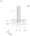
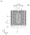
- FIG. 5 is a cross-sectional view of the circuit device 100.
- the circuit device 100 further has a sealing material 50.
- the sealing material 50 fills a space defined by two first partition plates 41 adjacent in the third direction DR3, two second partition plates 42 adjacent in the second direction DR2, and the upper surface 30a. .
- the first circuit component 10 (capacitor 10a) is arranged inside the sealing material 50 .
- the capacitor 10a has an exterior case 10aa, a sealing resin 10ab, a capacitor element body 10ac, and lead wires 10ad.
- the exterior case 10aa is filled with a sealing resin 10ab.
- a capacitor element body 10ac is arranged in the sealing resin 10ab.
- the capacitor element main body 10ac is formed by winding a dielectric film on which a metal foil is layered.
- the lead wire 10ad is electrically connected to the capacitor element body 10ac. A part of the lead wire 10ad is located outside the exterior case 10aa.
- the sealing material 50 has, for example, a heat dissipation auxiliary material 51 and a mold material 52 .
- the auxiliary heat dissipation material 51 is applied on the upper surface 30a.
- the auxiliary heat dissipation material 51 is in contact with the first circuit component 10 (capacitor 10a). More specifically, the auxiliary heat dissipation member 51 is in contact with the top surface of the exterior case 10aa.
- the molding material 52 is arranged on the heat radiation auxiliary material 51 .
- the molding material 52 is in contact with the first circuit component 10 (side surface of the exterior case 10aa), the first partition plate 41 and the second partition plate 42. As shown in FIG.
- the auxiliary heat dissipation material 51 is composed of an adhesive, grease, gel, or insulating sheet made of a resin material such as silicone resin, epoxy resin, or urethane resin.
- the auxiliary heat dissipation material 51 may be mixed with thermally conductive fillers such as ceramics or metals in order to improve thermal conductivity.
- the auxiliary heat dissipation material 51 may be a material having a thermal conductivity of, for example, 1 W/m ⁇ K to several tens of W/m ⁇ K.
- the molding material 52 is made of a resin material with high thermal conductivity.
- the molding material 52 is made of, for example, epoxy resin, silicone resin, urethane resin, PPS (polyphenylene sulfide) resin, PEEK (polyetheretherketone) resin, or ABS (acrylonitrile-butadiene-styrene) resin containing thermally conductive filler. may be configured.
- the Young's modulus of the molding material 52 may be 1 MPa or more and 50 GPa or less.
- the thermal conductivity of the molding material 52 may be 0.1 W/m ⁇ K or more and 20 W/m ⁇ K or less. Vibration resistance and environmental resistance are improved by sealing the molding material 52 .
- the auxiliary heat dissipation material 51 and the molding material 52 may be made of the same material.
- the auxiliary heat dissipation material 51 and the molding material 52 may be an adhesive.
- the circuit device 100 further has a printed wiring board 60 .
- the printed wiring board 60 is arranged on the first partition plate 41 and the second partition plate 42 .
- the printed wiring board 60 is electrically connected to the plurality of first circuit components 10 . More specifically, the terminals of the first circuit component 10 (the lead wires 10ad when the first circuit component 10 is the capacitor 10a) are inserted into the printed wiring board 60. As shown in FIG. Thus, the wiring of the peripheral circuit 110 shown in FIG. 1 is realized.
- the first partition plate 41 and the second partition plate 42 are attached to the upper surface 30a. More specifically, the first partition plate 41 is fitted into the second partition plate 42 with the second partition plate 42 arranged on the upper surface 30a. Secondly, a heat dissipation auxiliary material 51 is applied on the upper surface 30a. Third, the first circuit component 10 is arranged in a space defined by two adjacent first partition plates 41, two adjacent second partition plates 42, and the upper surface 30a. Fourth, a mold material 52 is injected into the space. Fifth, after the molding material 52 is cured, the first circuit component 10 and the printed wiring board 60 are connected. This connection is made, for example, by soldering.
- the top surface of the first circuit component 10 is in contact with the first heat sink 30 via the encapsulant 50 (heat dissipation auxiliary member 51). Further, in the circuit device 100, the side surfaces of the first circuit component 10 are in contact with the first partition plate 41 and the second partition plate 42 via the sealing material 50 (mold material 52). Therefore, the first circuit component 10 radiates heat from the side surfaces and the top surface, thereby improving the heat radiation performance.
- the life of the first circuit component 10 is improved.
- the first circuit component 10 is the capacitor 10a
- a temperature reduction of 10° C. approximately doubles the life.
- the first circuit component 10 is the inductor 10b
- the temperature reduction of 10° C. approximately doubles the life of the enamel coating of the inductor 10b.
- the first circuit component 10 is the discharge resistor 10d and the charge resistor 10e
- the temperature is reduced, so that the rank of the power category of the discharge resistor 10d and the charge resistor 10e can be lowered due to temperature derating.
- the number of series or parallel connections of the discharge resistor 10d and the charge resistor 10e can be reduced.
- heat diffusion heat radiation
- first partition plate 41 second partition plate 42
- an electrically optimal arrangement of the first circuit component 10 can be achieved without being subject to thermal restrictions.
- a plurality of first partition plates 41 and second partition plates 42 having high thermal conductivity are arranged. Therefore, the temperature of the first circuit component 10, which has different temperatures during normal operation, is equalized.
- the first circuit component 10 placed near the center of the circuit device 100 receives heat from the first circuit components 10 placed around it. temperature increases.
- the first circuit component 10 arranged in the outer peripheral portion of the circuit device 100 has a small temperature rise because there are few first circuit components 10 around it.
- the amount of temperature rise of the first circuit component 10 differs depending on the arrangement position, and a temperature difference occurs between the first circuit components 10 arranged at different positions.
- the plurality of the first partition plates 41 and the second partition plates 42 having high thermal conductivity are arranged, so that the temperature of the first circuit components 10 arranged in plurality can be equalized. can reduce the difference. Since the temperature derating is determined by the first circuit component 10 having the largest temperature rise, the circuit device 100 can be used more effectively when the temperature difference among the plurality of first circuit components 10 is smaller.
- the first partition plate 41 and the second partition plate 42 function as electromagnetic shields.
- the first circuit component 10 is the inductor 10b
- the leakage magnetic flux from the inductor 10b is shielded by the first partition plate 41 and the second partition plate 42, so that the sensor components (current sensor, etc.) can be improved.
- the first partition plate 41 and the second partition plate 42 function as firewalls.
- one of the first circuit components 10 is the capacitor 10a
- the sparks are blocked by the first partition plate 41 and the second partition plate 42, and other A shock to the 1-circuit component 10 is prevented.
- a space defined by two adjacent first partition plates 41, two adjacent second partition plates 42, and the upper surface 30a is filled with a sealing material 50 (mold material 52). Therefore, the vibration resistance characteristics of the first circuit component 10 can be improved.
- the circuit device 100 is a structure configured by combining the first partition plate 41 , the second partition plate 42 and the first heat sink 30 . Therefore, it is possible to increase or decrease the number of squares formed by the first partition plate 41 and the second partition plate 42 according to the number or size of the first circuit component 10 . Moreover, in the circuit device 100, the thickness, type, thickness, etc. of the first partition plate 41 and the second partition plate 42 can be arbitrarily selected. In addition, in the circuit device 100, the first partition plate 41 and the second partition plate 42 are subjected to bending and uneven press working to ensure the strength of the first partition plate 41 and the second partition plate 42 and to form a grid shape. mass shape changes are possible. As a result, the circuit device 100 can flexibly implement various specifications at low cost.
- the first circuit component 10 is arranged in the space defined by the two adjacent first partition plates 41, the two adjacent second partition plates 42, and the upper surface 30a.
- the insertion of the first circuit component 10 is easy, and the terminal position of the first circuit component 10 can be positioned at the same time as the insertion.
- the connection of the first circuit component 10 is performed by inserting the terminals of the first circuit component 10 into the printed wiring board 60, the assembly of the printed wiring board 60 is also easy.
- the connection between the first circuit components 10 is performed using the printed wiring board 60, the electrical connection between the first circuit components 10 can be freely performed.
- connection (soldering) between the terminals of the first circuit component 10 and the printed wiring board 60 can be performed using a flow solder bath or a point soldering device. That is, since the terminals of the first circuit component 10 and the printed wiring board 60 can be connected using the existing equipment, the equipment investment can be suppressed.
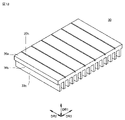
- FIG. 6 is a perspective view of a circuit device 100 according to a modification.
- circuit device 100 may further include case 70 .
- the case 70 is arranged on the upper surface 30 a so as to be positioned outside the first partition plate 41 and the second partition plate 42 .
- the first partition plate 41 and the second partition plate 42 are not fixed to the first heat sink 30 even if the first partition plate 41 and the second partition plate 42 are not fixed to the first heat sink 30.
- the space defined by the second partition plate 42 and the first heat sink 30 can be filled with the sealing material 50 .
- any of the capacitor 10a, the inductor 10b, the contactor 10c, the discharge resistor 10d, and the charge resistor 10e may be arranged as the first circuit component 10 used in the circuit device 100. Any component that generates heat can be used as the first circuit component 10 of the circuit device 100 without being limited to these.
- only one first circuit component 10 may be arranged in one section, or a plurality of first circuit components 10 may be arranged in one section.
- the one first circuit component 10 can use all the cooling capacity of the one section.
- the cooling capacity is divided, if the first circuit components 10 are small and the section is large, the first circuit components 10 can be arranged more efficiently. .
- the circuit device 100 may have a section (arrangement section) in which the first circuit component 10 is arranged and a section (non-arrangement section) in which the first circuit component 10 is not arranged.
- the cooling effect of the first circuit component 10 arranged in the arrangement section adjacent to the non-arrangement section can be further enhanced, and the first circuit component 10 can be cooled more effectively.
- circuit device 100A A circuit device (hereinafter referred to as "circuit device 100A") according to the second embodiment will be described. Here, differences from the circuit device 100 will be mainly described, and redundant description will not be repeated.
- FIG. 7 is a perspective view of the first heat sink 30 included in the circuit device 100A.
- a plurality of first grooves 30d and a plurality of second grooves 30e are formed in the upper surface 30a.
- the first groove 30d extends in the second direction DR2.
- the multiple first grooves 30d are spaced apart from each other in the third direction DR3.
- the second groove 30e extends in the third direction DR3.
- the multiple second grooves 30e are spaced apart from each other in the second direction DR2.
- FIG. 8 is a cross-sectional view of the circuit device 100A in the vicinity of the first groove 30d.
- FIG. 9 is a cross-sectional view of the circuit device 100A in the vicinity of the second groove 30e.
- the first partition plate 41 and the second partition plate 42 are inserted into the first groove 30d and the second groove 30e, respectively. More specifically, the first end 41a side of the first partition plate 41 and the third end 42a side of the second partition plate 42 are inserted into the first groove 30d and the second groove 30e, respectively.
- the first partition plate 41 and the second partition plate 42 are brazed to the first groove 30d and the second groove 30e with the brazing material 31, respectively. That is, the first partition plate 41 and the second partition plate 42 are metal-bonded to the first groove 30d and the second groove 30e, respectively.
- the first partition plate 41 and the second partition plate 42 may be welded (metallic joint) to the first groove 30d and the second groove 30e, respectively.
- the first partition plate 41 does not have to be brazed (welded) at all the portions inserted into the first grooves 30d.
- the second partition plate 42 does not need to be brazed (welded) at all portions disposed within the second grooves 30e.
- the first partition plate 41 and second partition plate 42 and the first heat sink 30 are metal-bonded. Since the contact thermal resistance is reduced, the heat dissipation performance of the first circuit component 10 is further improved.
- the first partition plate 41 and the second partition plate 42 are inserted into the first groove 30d and the second groove 30e, respectively.
- the positioning accuracy of the first partition plate 41 and the second partition plate 42 is improved. By improving the positioning accuracy, the distance between the first partition plate 41 and the second partition plate 42 and the first circuit component 10 (capacitor 10a) can be set with high accuracy. Thereby, the thickness of the sealing material 50 can be reduced, and the thermal resistance can be reduced. Furthermore, by fixing the first partition plate 41 and the second partition plate 42 to the first heat sink 30 , the space defined by the first partition plate 41 , the second partition plate 42 and the first heat sink 30 can be more reliably An encapsulant 50 can be filled.
- the first groove 30d may be formed to reach both ends of the upper surface 30a in the second direction DR2. In this case, when forming the first heat sink 30 by extrusion, the first groove 30d can be formed at the same time.
- the first groove 30d (second groove 30e) may be widened at the portion where it crosses the second groove 30e (first groove 30d). Further, the first groove 30d (second groove 30e) may be widened at the end in the second direction DR2 (third direction DR3). In these cases, it is possible to prevent the brazing filler metal 31 from overflowing from the first groove 30d (the second groove 30e) and resulting in manufacturing defects in the widened portion.
- circuit device 100B A circuit device (hereinafter referred to as "circuit device 100B") according to the third embodiment will be described. Here, differences from the circuit device 100A will be mainly described, and redundant description will not be repeated.
- FIG. 10 is a cross-sectional view of the circuit device 100B in the vicinity of the first groove 30d.
- FIG. 11 is a cross-sectional view of the circuit device 100B in the vicinity of the second groove 30e.
- the upper surface 30a is formed with caulked grooves 30fa and 30fb, and caulked grooves 30ga and 30gb.
- the crimped grooves 30fa and the crimped grooves 30fb extend in the second direction DR2.
- the caulking grooves 30fa and the caulking grooves 30fb are arranged so as to sandwich the first groove 30d in the third direction DR3.
- the crimped groove 30ga and the crimped groove 30gb extend in the third direction DR3.
- the caulking grooves 30fa and the caulking grooves 30fb are arranged so as to sandwich the second grooves 30e in the third direction DR3.
- the first partition plate 41 is crimped into the first groove 30d. More specifically, the portion of the first heat sink 30 between the first groove 30d and the crimped groove 30fa and the portion of the first heat sink 30 between the first groove 30d and the crimped groove 30fb are the first partition plates. The first partition plate 41 is crimped into the first groove 30d by plastic deformation toward the 41 side.
- the second partition plate 42 is crimped into the second groove 30e. More specifically, the portion of the first heat sink 30 between the second groove 30e and the crimped groove 30ga and the portion of the first heat sink 30 between the second groove 30e and the crimped groove 30gb are the second partition plates. The second partition plate 42 is crimped into the second groove 30e by being plastically deformed toward the 42 side.
- first partition plate 41 it is not necessary for the first partition plate 41 to be caulked at all portions inserted into the first grooves 30d. Further, the second partition plate 42 does not need to be caulked at all portions disposed within the second grooves 30e. For example, the crimping of the first partition plate 41 and the second partition plate 42 may not be performed at the portion where the first groove 30d and the second groove 30e intersect.
- first partition plate 41 second partition plate 42
- second partition plate 42 the other portion of the first partition plate 41 (second partition plate 42) is crimped. may This temporary fixation may be performed by spot welding.
- the first partition plate 41 and the second partition plate 42 and the first heat sink 30 are metal-bonded by caulking, and the first partition plate 41 and the second partition plate 42 and the first heat sink 30 Since the contact thermal resistance of the first circuit component 10 is reduced, the heat dissipation performance of the first circuit component 10 is further improved.
- the first partition plate 41 and the second partition plate 42 are inserted into the first groove 30d and the second groove 30e, respectively. In addition, the positioning accuracy of the first partition plate 41 and the second partition plate 42 is improved.
- the rest of the first partition plate 41 (second partition plate 42) is crimped.
- the position of the first partition plate 41 (second partition plate 42) can be finely adjusted after temporary fixing, the positional accuracy of the first partition plate 41 (second partition plate 42) can be further improved.
- a groove extending in the second direction DR2 may be formed in the lower surface 30b.
- the fins 30c may be configured by inserting plate members into the grooves. The crimping of the grooves of the plate member is performed by the same method as the crimping of the first partition plate 41 and the second partition plate 42, for example.
- circuit device 100C A circuit device (hereinafter referred to as "circuit device 100C") according to the fourth embodiment will be described. Here, differences from the circuit device 100 will be mainly described, and redundant description will not be repeated.
- FIG. 12 is a cross-sectional view of the circuit device 100C.
- FIG. 12 shows a cross section of the circuit device 100C at a position corresponding to FIG.
- the capacitor 10a does not have the exterior case 10aa and the sealing resin 10ab.
- the circuit device 100C further has an insulating net 11 .
- the insulating net 11 is made of an insulating resin material.
- the insulating net 11 is arranged in a space defined by two adjacent first partition plates 41, two adjacent second partition plates 42, and the upper surface 30a so as to cover the capacitor body 10ac. That is, the insulating net 11 is positioned between the capacitor element body 10ac and the upper surface 30a, between the capacitor element body 10ac and the first partition plate 41, and between the capacitor element body 10ac and the second partition plate 42. .
- the sealing material 50 does not have to be composed of the auxiliary heat dissipation material 51 and the molding material 52.
- the sealing material 50 is formed by potting an arbitrary resin material.
- This resin material is, for example, silicone.
- the insulating net 11 may be made of, for example, epoxy resin, silicone resin, urethane resin, PPS resin, PEEK resin, or ABS resin.
- the insulating net 11 may be made of a flexible and stretchable rubber material. Although the capacitor 10a and the insulating net 11 are not in contact in FIG. 12, the capacitor 10a and the insulating net 11 may be in contact. It is sufficient that the capacitor 10a is prevented from coming into contact with the first partition plate 41, the second partition plate 42 and the upper surface 30a by the insulating net 11.
- the capacitor 10a does not have the exterior case 10aa. Therefore, the cross-sectional area of the capacitor element body 10ac (the number of turns of the metal foil and the dielectric film in the capacitor element body 10ac) can be increased. Thus, according to the circuit device 100C, the capacitance per capacitor 10a can be increased.
- the insulating net 11 and the sealing material 50 are arranged between the capacitor 10a (capacitor element main body 10ac) and the upper surface 30a, the first partition plate 41 and the second partition plate 42, the exterior case 10aa and Even without the sealing resin 10ab, the insulation between the capacitor 10a (capacitor element body 10ac) and the upper surface 30a, the first partition plate 41 and the second partition plate 42 can be ensured.
- the capacitor 10a that does not have the exterior case 10aa can be used, so the cost of the capacitor 10a can be reduced.
- the capacitor 10a (capacitor element main body 10ac) can be sealed only with a resin having a low thermal resistance such as silicone as the sealing material 50. Therefore, the heat generated by the capacitor 10a is efficiently transferred to the first heat sink 30. can do.
- the insulating net 11 was used as a member for ensuring insulation between the capacitor 10a (capacitor element main body 10ac) and the upper surface 30a, the first partition plate 41 and the second partition plate 42.
- an insulating paper or a heat-conducting insulating sheet may be used.
- a spacer may be used instead of the insulating net 11. By disposing this spacer between capacitor element main body 10ac, first partition plate 41, second partition plate 42 and upper surface 30a, capacitor element main body 10ac, first partition plate 41, second partition plate 42 and upper surface 30a are separated from each other. Contact with 30a is prevented.
- circuit device 100D A circuit device (hereinafter referred to as “circuit device 100D”) according to Embodiment 5 will be described. Here, differences from the circuit device 100 will be mainly described, and redundant description will not be repeated.
- FIG. 13 is a perspective view of the first heat sink 30 included in the circuit device 100D. As shown in FIG. 13, grooves 30h are formed in the upper surface 30a. The groove 30h extends in the second direction DR2. Groove 30h is preferably formed to reach both ends of upper surface 30a in second direction DR2.
- FIG. 14 is a perspective view of the circuit device 100D.
- illustration of the sealing material 50 and the printed wiring board 60 is omitted.
- first partition plates 43 those arranged at both ends in the third direction DR3
- first partition plates 43 those arranged at other than both ends in the third direction DR3
- a partition plate 44 is used.
- second partition plates 45 those arranged at both ends in the second direction DR2 are referred to as second partition plates 45
- Two partition plates 46 are provided.
- FIG. 15 is a plan view of the first partition plate 43 included in the circuit device 100D. As shown in FIG. 15, in the first partition plate 43, the first insertion port 41c extends from the second end 41b toward the first end 41a.
- FIG. 16 is a plan view of the first partition plate 44 included in the circuit device 100D. As shown in FIG. 16, in the first partition plate 44, the first insertion port 41c extends from the first end 41a toward the second end 41b.
- FIG. 17 is a plan view of the second partition plate 45 included in the circuit device 100D. As shown in FIG. 17, in the second partition plate 45, the second insertion port 42ca extends from the third end 42a toward the fourth end 42b, and the second insertion port 42cb extends toward the fourth end 42b. , toward the third end 42a.
- the second partition plate 45 has a support portion 45a.
- the support portion 45a extends in the second direction DR2 on the side opposite to the second partition plate 46 .
- the support portion 45a is formed by bending the third end 42a side of the second partition plate 45 .
- the support portion 45a may be divided into a plurality of portions in the third direction DR3 (in the example of FIG. 17, a first portion 45aa, a second portion 45ab, a third portion 45ac, a fourth portion 45ad and a divided into a fifth portion 45ae).
- FIG. 18 is a plan view of the second partition plate 46 included in the circuit device 100D. As shown in FIG. 18, in the second partition plate 46, the second insertion port 42ca extends from the third end 42a toward the fourth end 42b, and the second insertion port 42cb extends toward the fourth end 42b. , toward the third end 42a.
- the width W at the third end 42a of the second insertion port 42ca of the second partition plate 45 is preferably larger than the width at the fourth end 42b of the second insertion port 42cb of the second partition plate 45. Also, the width W is larger than the width at the second end 41b of the first insertion port 41c of the first partition plate 43 and the width at the first end 41a of the first insertion port 41c of the first partition plate 44. is preferred. Furthermore, the width W is larger than the width at the third end 42a of the second insertion port 42ca of the second partition plate 46 and the width at the fourth end 42b of the second insertion port 42cb of the second partition plate 46. is preferred.
- the first partition plate 43, the first partition plate 44, the second partition plate 45, and the second partition plate 46 are attached to the upper surface 30a by the following method.
- the first partition plates 43 are inserted into the grooves 30h located at both ends in the third direction DR3.
- the second partition plate 45 is assembled to the first partition plate 43 by inserting the second insertion openings 42ca into the first insertion openings 41c of the first partition plate 43 located at both ends in the second direction DR2.
- the first partition plate 43 and the second partition plate 45 are generally upright.
- the second partition plate 46 is assembled to the first partition plate 43 by inserting the second insertion openings 42ca into the first insertion openings 41c of the first partition plate 43 located at positions other than both ends in the second direction DR2. .
- the width of the first insertion port 41c and the width of the second insertion port 42ca of the second partition plate 46 are smaller than the width W. can also be easily inserted. Since the first partition plate 43 and the second partition plate 45 are already substantially upright, the second partition plate 46 is also substantially upright.
- the first partition plate 44 is connected to the second partition plate 45 and the second partition plate 46.
- the width of the first insertion port 41c and the width of the second insertion port 42cb are smaller than the width W. can also be easily inserted.
- the first partition plate 44 is inserted into the grooves 30h positioned other than both ends in the third direction DR3.
- first partition plate 43, the first partition plate 44, the second partition plate 45 and the second partition plate 46 are fixed to the upper surface 30a.
- the fixing of the first partition plate 43 and the first partition plate 44 to the upper surface 30a is performed, for example, by caulking the grooves 30h.
- the fixing of the second partition plate 45 and the second partition plate 46 to the upper surface 30a is performed by fillet welding, for example.
- the step of forming the grooves can be simplified. Since the groove 30h extends in the second direction DR2 (the same direction as the fins 30c), it can be formed at the same time as the first heat sink 30 is formed by extrusion.
- the assembly of the first partition plate 43, the first partition plate 44, the second partition plate 45, and the second partition plate 46 can be performed with minimum holding, so that the assembly process can be automated. It is possible to reduce man-hours and simplify jigs.
- the second partition plate 45 may be used instead of the second partition plate 46 . In this case, it is possible to reduce the manufacturing cost by sharing the members.
- Modification 2 In the circuit device 100D, some of the plurality of portions included in the support portion 45a may be bent in opposite directions.
- the first portion 45aa, the second portion 45ac, and the fifth portion 45ae extend in the third direction DR3 on the side opposite to the second partition plate 46, while the second portion 45ab and the fourth portion 45ad It may extend in the third direction DR3 toward the second partition plate 46 side. In this case, the uprightness of the second partition plate 45 can be further enhanced.
- the second partition plate 45 may be fixed to the first heat sink 30 by screwing instead of welding. More specifically, a screw hole is formed in the upper surface 30a, a through hole is formed in the support portion 45a so as to overlap the screw hole, and a screw inserted into the through hole is screwed into the screw hole. , the second partition plate 45 may be fixed to the first heat sink 30 . In this case, since the second partition plate 45 can be firmly attached to the upper surface 30a, the thermal contact resistance between the second partition plate 45 and the upper surface 30a can be reduced. When the screwing is performed in the area where the first circuit component 10 is arranged, it is preferable to prevent the head of the screw from protruding by performing countersunk screw processing on the support portion 45a. .
- circuit device 100E A circuit device (hereinafter referred to as "circuit device 100E") according to Embodiment 6 will be described. Here, differences from the circuit device 100 will be mainly described, and redundant description will not be repeated.
- FIG. 19 is a perspective view of the circuit device 100E. As shown in FIG. 19, circuit device 100E further includes second heat sink 80 and heat pipe 90 . In addition, in the circuit device 100E, the first heat sink 30 does not have the fins 30c.
- the second heat sink 80 has an upper surface 80a and a lower surface 80b.
- the second circuit component 20 is arranged on the upper surface 80a.
- the lower surface 80b is the opposite surface of the upper surface 80a.
- a plurality of fins 80c are formed on the lower surface 80b.
- the heat pipe 90 thermally connects the first heat sink 30 and the second heat sink 80 . More specifically, the heat pipe 90 is filled with a liquid (for example, pure water). Pure water in the heat pipe 90 evaporates due to heat from the first heat sink 30 . That is, the pure water in the heat pipe 90 absorbs latent heat of evaporation from the first heat sink 30 and cools the first heat sink 30 . The evaporated pure water in the heat pipe 90 moves to the second heat sink 80 side. The portion of heat pipe 90 between first heat sink 30 and second heat sink 80 is insulated.
- a liquid for example, pure water
- the pure water in the heat pipe 90 that has moved toward the second heat sink 80 releases latent heat of evaporation to the second heat sink 80 and condenses.
- the condensed pure water in the heat pipe 90 returns to the first heat sink 30 side due to the capillary structure (wick) provided on the inner wall of the heat pipe 90 .
- the first heat sink 30 and the second heat sink 80 are thermally connected by the heat pipe 90 .
- the heat from the first heat sink 30 radiated to the second heat sink 80 is intensively radiated by the second heat sink 80 .
- the heat pipe 90 does not have to pass through the interior of the first heat sink 30 and the second heat sink 80 .
- the heat pipe 90 should be in contact with at least the first heat sink 30 and the second heat sink 80 .
- circuit device 100E fect of circuit device 100E
- the first heat sink 30 can be simplified and miniaturized, the volume and cost of the first heat sink 30 can be reduced.
- the circuit device 100E does not require an individual cooling space such as an air passage, the space efficiency of the device as a whole is improved, so that the device can be made smaller.
- the first heat sink 30 can be arranged at any location. More specifically, the first heat sink 30 can be arranged in an electrically optimal place, for example, in the vicinity of the second circuit component 20 or in a place where the wiring length can be shortened (wiring inductance can be reduced). .
- the electrical performance of the entire device or the switching circuit 120 can be improved. For example, it is possible to reduce loss associated with shortening the wiring length, and suppress switching surges associated with reducing the wiring inductance.
- circuit device 100F A circuit device (hereinafter referred to as "circuit device 100F") according to Embodiment 7 will be described. Here, differences from the circuit device 100 will be mainly described, and redundant description will not be repeated.
- FIG. 20 is a perspective view of the circuit device 100F. In FIG. 20, illustration of the printed wiring board 60 is omitted.
- FIG. 21 is a cross-sectional view of the circuit device 100F. FIG. 21 shows a cross section of the circuit device 100F at a position corresponding to FIG. As shown in FIGS. 20 and 21, in the circuit device 100F, slits 53 and slits 54 are formed in the surface of the sealing material 50 (molding material 52) on the printed wiring board 60 side.
- the slit 53 extends in the second direction DR2.
- the slit 54 extends in the third direction DR3.
- the slits 53 and 54 have, for example, a U shape in cross-sectional view perpendicular to their extending directions.
- the slits 53 and 54 may have a V shape in a cross-sectional view orthogonal to their extending directions. Either one of the slit 53 and the slit 54 may not be formed.
- the width of the slit 53 and the width of the slit 54 are preferably 1 mm or more.
- the formation of the slits 53 and the formation of the slits 54 may be performed after the sealing material 50 (mold material 52) is cured, or may be performed before the sealing material 50 (mold material 52) is cured.
- Capacitor 10a may expand when it fails. In the circuit device 100F, stress tends to concentrate on the portion where the slit 53 is formed and the portion where the slit 54 is formed, and the strength is relatively low in these portions. Therefore, in the circuit device 100F, even if the capacitor 10a expands due to a failure, the sealing material 50 (mold material 52) is broken near the slits 53 and 54 to alleviate the force associated with the expansion. Explosion of the sealing material 50 (mold material 52) can be suppressed.
- the slits 53 and 54 are formed, so that the insulation distance between the two terminals of the capacitor 10a can be increased.
- the slits 53 and 54 are formed before the sealing material 50 (mold material 52) is cured, thereby suppressing the occurrence of short circuits due to dust and conductive foreign matter generated during the slit forming process.
- circuit device 100G A circuit device (hereinafter referred to as “circuit device 100G”) according to Embodiment 8 will be described. Here, differences from the circuit device 100 will be mainly described, and redundant description will not be repeated.
- FIG. 22 is a cross-sectional view of the circuit device 100G.
- FIG. 22 shows a cross section of the circuit device 100G at a position corresponding to FIG.
- silicone gel 55 is used in place of molding material 52 in circuit device 100G.
- the silicone gel 55 is made of a material with low viscosity.
- the silicone gel 55 may be used instead of the sealing material 50 (see FIG. 12) in the circuit device 100C.
- the silicone gel 55 has high insulating performance.
- the silicone gel 55 since the silicone gel 55 has high adhesion to the capacitor 10a, the first partition plate 41 and the second partition plate 42, there is no need to consider the creepage at the boundary with these parts/members. This eliminates the need for an insulating area for securing the creepage surface, making it possible to reduce the size of the periphery of the capacitor 10a.
- the use of the silicone gel 55 can ensure high insulation (high creeping dielectric strength and penetration dielectric strength).
- the heat radiation performance from the capacitor 10a can be improved at the same time.
- the silicone gel 55 is a highly penetrating (soft) material, the reliability of the circuit device 100G is improved when heat cycles or power cycles are applied. Since the capacitor 10a is also fixed in position by the printed wiring board 60, even if the silicone gel 55 is used, the positional fixation of the capacitor 10a is not hindered.
- Second circuit component 10 First circuit component 10a Capacitor 10aa Exterior case 10ab Sealing resin 10ad Lead wire 10b Inductor 10c Contactor 10d Discharging resistor 10e Charging resistor 11 Insulating net 20 Second circuit component 20a, 20b, 20c, 20d, 20e, 20f transistors, 20g, 20h, 20i, 20j, 20k, 20l diodes, 30 first heat sink, 30a upper surface, 30b lower surface, 30c fins, 30d first groove, 30e second groove, 30fa, 30fb, 30ga, 30gb crimped groove, 30h groove, 31 brazing material, 41 first partition plate, 41a first end, 41b second end, 41c first insertion port, 42 second partition plate, 42a third end, 42b fourth end , 42c, 42ca, 42cb second insertion port, 43, 44 first partition plate, 45 second partition plate, 45a support portion, 45aa first portion, 45ab second portion, 45ad fourth portion, 45ae fifth portion, 46 Second
Landscapes
- Engineering & Computer Science (AREA)
- Microelectronics & Electronic Packaging (AREA)
- Power Engineering (AREA)
- Physics & Mathematics (AREA)
- Thermal Sciences (AREA)
- Manufacturing & Machinery (AREA)
- Cooling Or The Like Of Electrical Apparatus (AREA)
Priority Applications (2)
| Application Number | Priority Date | Filing Date | Title |
|---|---|---|---|
| US18/559,574 US12477694B2 (en) | 2021-06-22 | 2022-06-14 | Circuit device |
| JP2023530339A JP7634673B2 (ja) | 2021-06-22 | 2022-06-14 | 回路装置 |
Applications Claiming Priority (2)
| Application Number | Priority Date | Filing Date | Title |
|---|---|---|---|
| JP2021103422 | 2021-06-22 | ||
| JP2021-103422 | 2021-06-22 |
Publications (1)
| Publication Number | Publication Date |
|---|---|
| WO2022270352A1 true WO2022270352A1 (ja) | 2022-12-29 |
Family
ID=84544989
Family Applications (1)
| Application Number | Title | Priority Date | Filing Date |
|---|---|---|---|
| PCT/JP2022/023769 Ceased WO2022270352A1 (ja) | 2021-06-22 | 2022-06-14 | 回路装置 |
Country Status (3)
| Country | Link |
|---|---|
| US (1) | US12477694B2 (https=) |
| JP (1) | JP7634673B2 (https=) |
| WO (1) | WO2022270352A1 (https=) |
Cited By (3)
| Publication number | Priority date | Publication date | Assignee | Title |
|---|---|---|---|---|
| WO2026004494A1 (ja) * | 2024-06-24 | 2026-01-02 | 株式会社デンソー | コンデンサモジュール |
| WO2026043089A1 (ko) * | 2024-08-21 | 2026-02-26 | 엘에스일렉트릭 주식회사 | 전력 소자 모듈 |
| KR102956188B1 (ko) * | 2024-08-21 | 2026-04-22 | 엘에스일렉트릭(주) | 전력 소자 모듈 |
Citations (5)
| Publication number | Priority date | Publication date | Assignee | Title |
|---|---|---|---|---|
| JPH10116756A (ja) * | 1996-10-11 | 1998-05-06 | Honda Motor Co Ltd | コンデンサ |
| JP2000195748A (ja) * | 1998-12-25 | 2000-07-14 | Matsushita Electric Ind Co Ltd | コンデンサ |
| JP2014116400A (ja) * | 2012-12-07 | 2014-06-26 | Toyota Motor Corp | コンデンサモジュール |
| WO2016117441A1 (ja) * | 2015-01-22 | 2016-07-28 | カルソニックカンセイ株式会社 | コンデンサ構造 |
| JP2019179856A (ja) * | 2018-03-30 | 2019-10-17 | 日本ケミコン株式会社 | 蓄電デバイスモジュール及び蓄電デバイスホルダー |
Family Cites Families (4)
| Publication number | Priority date | Publication date | Assignee | Title |
|---|---|---|---|---|
| JP2016066666A (ja) | 2014-09-24 | 2016-04-28 | 株式会社指月電機製作所 | コンデンサ |
| CN112042092B (zh) * | 2018-04-25 | 2024-03-01 | 松下知识产权经营株式会社 | 电源装置 |
| CN114342232A (zh) * | 2019-09-09 | 2022-04-12 | 三菱电机株式会社 | 电力转换装置及电力转换装置的制造方法 |
| JP6961047B1 (ja) | 2020-07-17 | 2021-11-05 | 三菱電機株式会社 | 電力変換装置 |
-
2022
- 2022-06-14 WO PCT/JP2022/023769 patent/WO2022270352A1/ja not_active Ceased
- 2022-06-14 US US18/559,574 patent/US12477694B2/en active Active
- 2022-06-14 JP JP2023530339A patent/JP7634673B2/ja active Active
Patent Citations (5)
| Publication number | Priority date | Publication date | Assignee | Title |
|---|---|---|---|---|
| JPH10116756A (ja) * | 1996-10-11 | 1998-05-06 | Honda Motor Co Ltd | コンデンサ |
| JP2000195748A (ja) * | 1998-12-25 | 2000-07-14 | Matsushita Electric Ind Co Ltd | コンデンサ |
| JP2014116400A (ja) * | 2012-12-07 | 2014-06-26 | Toyota Motor Corp | コンデンサモジュール |
| WO2016117441A1 (ja) * | 2015-01-22 | 2016-07-28 | カルソニックカンセイ株式会社 | コンデンサ構造 |
| JP2019179856A (ja) * | 2018-03-30 | 2019-10-17 | 日本ケミコン株式会社 | 蓄電デバイスモジュール及び蓄電デバイスホルダー |
Cited By (3)
| Publication number | Priority date | Publication date | Assignee | Title |
|---|---|---|---|---|
| WO2026004494A1 (ja) * | 2024-06-24 | 2026-01-02 | 株式会社デンソー | コンデンサモジュール |
| WO2026043089A1 (ko) * | 2024-08-21 | 2026-02-26 | 엘에스일렉트릭 주식회사 | 전력 소자 모듈 |
| KR102956188B1 (ko) * | 2024-08-21 | 2026-04-22 | 엘에스일렉트릭(주) | 전력 소자 모듈 |
Also Published As
| Publication number | Publication date |
|---|---|
| US20240244796A1 (en) | 2024-07-18 |
| JP7634673B2 (ja) | 2025-02-21 |
| JPWO2022270352A1 (https=) | 2022-12-29 |
| US12477694B2 (en) | 2025-11-18 |
Similar Documents
| Publication | Publication Date | Title |
|---|---|---|
| JP5382049B2 (ja) | 半導体装置 | |
| JP5217884B2 (ja) | 半導体装置 | |
| US7151661B2 (en) | Capacitor module and semiconductor device using the same | |
| CN104066291B (zh) | 外壳及具有该外壳的电源模块 | |
| US11062972B2 (en) | Electronic module for power control and method for manufacturing an electronic module power control | |
| WO2014184846A1 (ja) | 電子モジュールおよびその製造方法 | |
| US9491844B2 (en) | Electronic device | |
| JP7634673B2 (ja) | 回路装置 | |
| JP7566020B2 (ja) | 電力変換装置 | |
| JP2021093485A (ja) | 電力変換装置、及び電力変換装置の製造方法 | |
| CN114631400B (zh) | 带传热构件的基板以及带传热构件的基板的制造方法 | |
| US12183498B2 (en) | Power conversion device | |
| JP2005045960A (ja) | 電力変換装置 | |
| JP7809235B2 (ja) | 電力変換装置 | |
| WO2020080248A1 (ja) | 回路構造体及び電気接続箱 | |
| JP5621812B2 (ja) | 半導体装置 | |
| JP7088124B2 (ja) | 半導体装置 | |
| JP7634674B2 (ja) | 回路装置 | |
| JP2016096190A (ja) | 電子装置 | |
| JP2026010714A (ja) | 接続導体の冷却装置 | |
| JP2009188192A (ja) | 回路装置 | |
| JP2024031507A (ja) | サージ抑制装置 | |
| JP2016092868A (ja) | 積層ユニット | |
| JP5069587B2 (ja) | 回路装置 | |
| CN120388968A (zh) | 半导体模块 |
Legal Events
| Date | Code | Title | Description |
|---|---|---|---|
| 121 | Ep: the epo has been informed by wipo that ep was designated in this application |
Ref document number: 22828269 Country of ref document: EP Kind code of ref document: A1 |
|
| WWE | Wipo information: entry into national phase |
Ref document number: 2023530339 Country of ref document: JP |
|
| WWE | Wipo information: entry into national phase |
Ref document number: 18559574 Country of ref document: US |
|
| NENP | Non-entry into the national phase |
Ref country code: DE |
|
| 122 | Ep: pct application non-entry in european phase |
Ref document number: 22828269 Country of ref document: EP Kind code of ref document: A1 |
|
| WWG | Wipo information: grant in national office |
Ref document number: 18559574 Country of ref document: US |