WO2022264393A1 - 光センサ装置 - Google Patents
光センサ装置 Download PDFInfo
- Publication number
- WO2022264393A1 WO2022264393A1 PCT/JP2021/023157 JP2021023157W WO2022264393A1 WO 2022264393 A1 WO2022264393 A1 WO 2022264393A1 JP 2021023157 W JP2021023157 W JP 2021023157W WO 2022264393 A1 WO2022264393 A1 WO 2022264393A1
- Authority
- WO
- WIPO (PCT)
- Prior art keywords
- signal
- frequency
- optical
- analog
- light
- Prior art date
- Legal status (The legal status is an assumption and is not a legal conclusion. Google has not performed a legal analysis and makes no representation as to the accuracy of the status listed.)
- Ceased
Links
Images







Classifications
-
- G—PHYSICS
- G01—MEASURING; TESTING
- G01B—MEASURING LENGTH, THICKNESS OR SIMILAR LINEAR DIMENSIONS; MEASURING ANGLES; MEASURING AREAS; MEASURING IRREGULARITIES OF SURFACES OR CONTOURS
- G01B9/00—Measuring instruments characterised by the use of optical techniques
- G01B9/02—Interferometers
- G01B9/02001—Interferometers characterised by controlling or generating intrinsic radiation properties
- G01B9/02002—Interferometers characterised by controlling or generating intrinsic radiation properties using two or more frequencies
- G01B9/02003—Interferometers characterised by controlling or generating intrinsic radiation properties using two or more frequencies using beat frequencies
-
- G—PHYSICS
- G01—MEASURING; TESTING
- G01C—MEASURING DISTANCES, LEVELS OR BEARINGS; SURVEYING; NAVIGATION; GYROSCOPIC INSTRUMENTS; PHOTOGRAMMETRY OR VIDEOGRAMMETRY
- G01C3/00—Measuring distances in line of sight; Optical rangefinders
- G01C3/02—Details
- G01C3/06—Use of electric means to obtain final indication
-
- G—PHYSICS
- G01—MEASURING; TESTING
- G01N—INVESTIGATING OR ANALYSING MATERIALS BY DETERMINING THEIR CHEMICAL OR PHYSICAL PROPERTIES
- G01N21/00—Investigating or analysing materials by the use of optical means, i.e. using sub-millimetre waves, infrared, visible or ultraviolet light
- G01N21/17—Systems in which incident light is modified in accordance with the properties of the material investigated
-
- G—PHYSICS
- G01—MEASURING; TESTING
- G01B—MEASURING LENGTH, THICKNESS OR SIMILAR LINEAR DIMENSIONS; MEASURING ANGLES; MEASURING AREAS; MEASURING IRREGULARITIES OF SURFACES OR CONTOURS
- G01B9/00—Measuring instruments characterised by the use of optical techniques
- G01B9/02—Interferometers
- G01B9/02001—Interferometers characterised by controlling or generating intrinsic radiation properties
- G01B9/02002—Interferometers characterised by controlling or generating intrinsic radiation properties using two or more frequencies
- G01B9/02004—Interferometers characterised by controlling or generating intrinsic radiation properties using two or more frequencies using frequency scans
-
- G—PHYSICS
- G01—MEASURING; TESTING
- G01D—MEASURING NOT SPECIALLY ADAPTED FOR A SPECIFIC VARIABLE; ARRANGEMENTS FOR MEASURING TWO OR MORE VARIABLES NOT COVERED IN A SINGLE OTHER SUBCLASS; TARIFF METERING APPARATUS; MEASURING OR TESTING NOT OTHERWISE PROVIDED FOR
- G01D5/00—Mechanical means for transferring the output of a sensing member; Means for converting the output of a sensing member to another variable where the form or nature of the sensing member does not constrain the means for converting; Transducers not specially adapted for a specific variable
- G01D5/26—Mechanical means for transferring the output of a sensing member; Means for converting the output of a sensing member to another variable where the form or nature of the sensing member does not constrain the means for converting; Transducers not specially adapted for a specific variable characterised by optical transfer means, i.e. using infrared, visible, or ultraviolet light
-
- G—PHYSICS
- G01—MEASURING; TESTING
- G01S—RADIO DIRECTION-FINDING; RADIO NAVIGATION; DETERMINING DISTANCE OR VELOCITY BY USE OF RADIO WAVES; LOCATING OR PRESENCE-DETECTING BY USE OF THE REFLECTION OR RERADIATION OF RADIO WAVES; ANALOGOUS ARRANGEMENTS USING OTHER WAVES
- G01S17/00—Systems using the reflection or reradiation of electromagnetic waves other than radio waves, e.g. lidar systems
- G01S17/02—Systems using the reflection of electromagnetic waves other than radio waves
- G01S17/06—Systems determining position data of a target
-
- G—PHYSICS
- G01—MEASURING; TESTING
- G01S—RADIO DIRECTION-FINDING; RADIO NAVIGATION; DETERMINING DISTANCE OR VELOCITY BY USE OF RADIO WAVES; LOCATING OR PRESENCE-DETECTING BY USE OF THE REFLECTION OR RERADIATION OF RADIO WAVES; ANALOGOUS ARRANGEMENTS USING OTHER WAVES
- G01S17/00—Systems using the reflection or reradiation of electromagnetic waves other than radio waves, e.g. lidar systems
- G01S17/02—Systems using the reflection of electromagnetic waves other than radio waves
- G01S17/06—Systems determining position data of a target
- G01S17/08—Systems determining position data of a target for measuring distance only
- G01S17/32—Systems determining position data of a target for measuring distance only using transmission of continuous waves, whether amplitude-, frequency-, or phase-modulated, or unmodulated
- G01S17/34—Systems determining position data of a target for measuring distance only using transmission of continuous waves, whether amplitude-, frequency-, or phase-modulated, or unmodulated using transmission of continuous, frequency-modulated waves while heterodyning the received signal, or a signal derived therefrom, with a locally-generated signal related to the contemporaneously transmitted signal
-
- G—PHYSICS
- G01—MEASURING; TESTING
- G01S—RADIO DIRECTION-FINDING; RADIO NAVIGATION; DETERMINING DISTANCE OR VELOCITY BY USE OF RADIO WAVES; LOCATING OR PRESENCE-DETECTING BY USE OF THE REFLECTION OR RERADIATION OF RADIO WAVES; ANALOGOUS ARRANGEMENTS USING OTHER WAVES
- G01S7/00—Details of systems according to groups G01S13/00, G01S15/00, G01S17/00
- G01S7/48—Details of systems according to groups G01S13/00, G01S15/00, G01S17/00 of systems according to group G01S17/00
- G01S7/497—Means for monitoring or calibrating
-
- A—HUMAN NECESSITIES
- A61—MEDICAL OR VETERINARY SCIENCE; HYGIENE
- A61B—DIAGNOSIS; SURGERY; IDENTIFICATION
- A61B3/00—Apparatus for testing the eyes; Instruments for examining the eyes
- A61B3/10—Objective types, i.e. instruments for examining the eyes independent of the patients' perceptions or reactions
- A61B3/102—Objective types, i.e. instruments for examining the eyes independent of the patients' perceptions or reactions for optical coherence tomography [OCT]
Definitions
- the present disclosure relates to an optical sensor device.
- a wavelength-swept optical coherence tomography (SS-OCT: Swept Source-OCT) that employs a wavelength-scanning interference method splits wavelength-swept light, whose frequency changes over time, into signal light and reference light.
- SS-OCT emits branched signal light toward a measurement target, receives signal light reflected by the measurement target, and causes the received signal light to interfere with the branched reference light to generate interference light. to obtain the beat signal.
- SS-OCT measures the distance from the light source to the measurement target by measuring the frequency of the acquired beat signal.
- the optical distance measuring device described in Patent Document 1 compensates for such nonlinearity of the wavelength swept light. More specifically, the optical distance measuring device uses a laser light source with a known frequency-modulated waveform, and performs regression analysis on the beat signal based on the known frequency-modulated waveform by digital signal processing to determine the wavelength. Compensate for the nonlinearity of the swept light.
- Patent Document 1 requires regression analysis for each measurement to compensate for the nonlinearity of the wavelength-swept light, which poses a problem of increased signal processing load.
- the present disclosure has been made to solve the above problems, and provides a technique for reducing the signal processing load caused by compensating for the nonlinearity of wavelength-swept light.
- the optical sensor device includes a wavelength swept light source that outputs light whose frequency changes over time, an optical splitter that splits the light output from the wavelength swept light source 1 into signal light and local light, and an optical splitter.
- the signal light branched by the device is emitted toward the measurement target, and the optical sensor head receives the reflected light reflected by the measurement target, the local light branched by the optical branching device, and the optical sensor head receive An optical heterodyne receiver that obtains a received signal as an electrical signal by combining reflected light and photoelectrically converting the combined light, and converting the received signal obtained by the optical heterodyne receiver into a digital signal by sampling.
- a first digital-to-analog converter that generates a first clock signal for the analog-to-digital converter; and a signal that calculates measurement data relating to the object to be measured based on the received signal converted into a digital signal by the analog-to-digital converter.
- the optical heterodyne receiver multiplexes the local light split by the optical splitter and the internally reflected light obtained by internally reflecting the signal light split by the optical splitter, and multiplexes them.
- the analog-to-digital converter further converts the internal received signal obtained by the optical heterodyne receiver into a digital signal by sampling
- the signal processing device based on the internal received signal converted into a digital signal by the analog-to-digital converter, further calculates first frequency fluctuation reference signal data as a reference for the frequency fluctuation of the light output from the wavelength swept light source
- the first digital-to-analog converter converts the first frequency variation reference signal data calculated by the signal processing device into an analog signal to generate a first frequency variation reference signal as a first clock signal
- the received signal acquired by the optical heterodyne receiver is sampled in synchronization with the first frequency-varying reference signal generated by the digital-to-analog converter.
- the signal processing load caused by compensating for the nonlinearity of the wavelength swept light is reduced.
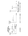
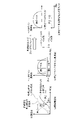
- FIG. 1 is a block diagram showing the configuration of an optical sensor device according to Embodiment 1;
- FIG. 10 is a graph showing temporal changes in the frequency of an internal received signal obtained by an optical heterodyne receiver combining local light and internal reflected light and photoelectrically exchanging the combined light in a specific example of Embodiment 4; FIG. .
- FIG. 13A is a block diagram showing a hardware configuration that implements the functions of the signal processing device according to Embodiments 1-4.
- FIG. 13B is a block diagram showing a hardware configuration for executing software realizing the functions of the signal processing device according to Embodiments 1-4.
- FIG. 1 is a block diagram showing the configuration of an optical sensor device 1000 according to Embodiment 1.
- the optical sensor device 1000 includes a wavelength swept light source 1, an optical splitter 2, an optical circulator 3, a reference reflection point 4, an optical sensor head 5, an optical heterodyne receiver 6, and an analog-to-digital converter 7 (ADC). , a digital-analog converter 8 (DAC) (first digital-analog converter), a signal processor 9 , a reference clock 10 , a splitter 11 , a phase-locked loop 12 (PLL), and a switch 13 .
- DAC digital-analog converter 8
- PLL phase-locked loop 12
- the wavelength swept light source 1 outputs light whose frequency changes over time (wavelength swept light) to the optical splitter 2 . That is, the wavelength swept light source 1 performs frequency sweep (wavelength sweep). In other words, the swept wavelength light source 1 outputs light whose wavelength changes with time to the optical branching device 2 .
- the wavelength swept light source 1 it is possible to use a laser light source whose wavelength is controllable by controlling the cavity length, or a laser light source whose wavelength changes depending on the amount of injected current.
- the swept wavelength light source 1 may output light that alternately repeats continuous triangular up-chirp and down-chirp by sweeping the frequency, or output light that repeats sawtooth-wave up-chirp.
- light that repeats a sawtooth-like down-chirp may be output, or a chirped pulse signal of pulsed up-chirp or down-chirp may be output.
- the optical splitter 2 splits the light output from the wavelength swept light source into signal light and local light.
- the optical splitter 2 outputs the split signal light to the optical circulator 3, and outputs the split local light to the optical heterodyne receiver 6 (22 in FIG. 1).
- the optical circulator 3 outputs the signal light split by the optical splitter 2 to the reference reflection point 4 .
- the reference reflection point 4 internally reflects the signal light split by the optical splitter 2 by partially reflecting it. More specifically, in the first embodiment, the reference reflection point 4 internally reflects the signal light output from the optical circulator 3 by partially reflecting it. Internally reflected light internally reflected by the reference reflection point 4 is output to the optical heterodyne receiver 6 via the optical circulator 3 . The signal light that has passed through the reference reflection point 4 is output to the optical sensor head 5 .
- Examples of reference reflection points 4 include partially reflecting mirrors or connector end faces.
- the optical sensor head 5 emits the signal light (51 in FIG. 1) branched by the optical splitter 2 toward the measurement target 999, and receives the reflected light (51 in FIG. 1) reflected by the measurement target 999. . More specifically, in the first embodiment, the optical sensor head 5 emits the signal light (51 in FIG. 1) that has passed through the reference reflection point 4 toward the measurement target 999, and receives the signal light reflected by the measurement target 999. Receive light (51 in FIG. 1). The optical sensor head 5 outputs the received reflected light to the optical heterodyne receiver 6 via the reference reflection point 4 and the optical circulator 3 (31 in FIG. 1).
- the optical circulator 3 outputs the signal light (21 in FIG. 1) input from the optical splitter 2 side to the reference reflection point 4, and the reflected light input from the reference reflection point 4 side or The internally reflected light ( 31 in FIG. 1) is output to the optical heterodyne receiver 6 .
- the optical heterodyne receiver 6 multiplexes the local light (22 in FIG. 1) branched by the optical splitter 2 and the reflected light (31 in FIG. 1) received by the optical sensor head 5, and outputs the combined light.
- a reception signal (beat signal) as an electric signal is obtained by photoelectric conversion. That is, the optical heterodyne receiver 6 heterodynes the local light (22 in FIG. 1) split by the optical splitter 2 and the reflected light (31 in FIG. 1) received by the optical sensor head 5.
- the optical heterodyne receiver 6 photoelectrically converts the combined light using, for example, a photodiode (PD).
- PD photodiode
- the optical heterodyne receiver 6 receives the local light (22 in FIG. 1) split by the optical splitter 2 and the internally reflected light (22 in FIG. 1) obtained by internally reflecting the signal light split by the optical splitter 2. 31) and photoelectrically convert the combined light to obtain an internal received signal as an electrical signal. More specifically, the optical heterodyne receiver 6 combines the local light (22 in FIG. 1) split by the optical splitter 2 and the internal reflected light (31 in FIG. 1) reflected by the reference reflection point 4. By photoelectrically converting the combined light, an internal received signal as an electrical signal is further obtained. The optical heterodyne receiver 6 outputs the acquired received signal and internal received signal (61 in FIG. 1) to the analog-to-digital converter 7, respectively.
- the reference clock 10 generates a reference clock signal.
- the reference clock 10 outputs the generated reference clock signal to the splitter 11 .
- Brancher 11 branches the reference clock signal generated by reference clock 10 to signal processing device 9 and phase-locked loop 12 .
- phase-locked loop 12 generates a second clock signal for the analog-to-digital converter 7 . More specifically, in the first embodiment, phase-locked loop 12 generates the second clock signal for analog-to-digital converter 7 in synchronization with the reference clock signal branched by splitter 11 . The phase-locked loop 12 outputs the generated second clock signal (121 in FIG. 1) to the digital-analog converter 8 and outputs the generated second clock signal (122 in FIG. 1) to the switch 13.
- a digital-to-analog converter 8 (DAC) generates a first clock signal for the analog-to-digital converter 7 . More specifically, the digital-to-analog converter 8 generates the first clock signal for the analog-to-digital converter 7 in synchronization with the second clock signal generated by the phase-locked loop 12 . The digital-to-analog converter 8 outputs the generated first clock signal ( 81 in FIG. 1) to the switch 13 . Details of the first clock signal will be described later.
- the digital-to-analog converter 8 is configured to generate the first clock signal for the analog-to-digital converter 7 in synchronization with the second clock signal generated by the phase-locked loop 12.
- the optical sensor device 1000 may additionally include a circuit that generates a clock, and the digital-to-analog converter 8 generates the first clock signal of the analog-to-digital converter 7 in synchronization with the clock generated by the circuit. may be generated. That is, the frequency of the first clock signal and the frequency of the second clock signal need not be synchronized.
- the switch 13 switches the clock signal of the analog-to-digital converter 7 to either the first clock signal generated by the digital-to-analog converter 8 or the second clock signal generated by the phase-locked loop 12 .
- the switch 13 changes the clock signal of the analog-to-digital converter 7 to the second clock signal generated by the phase-locked loop 12.
- the switch 13 switches the clock signal of the analog-to-digital converter 7 to the first clock signal generated by the digital-to-analog converter 8 .
- the analog-to-digital converter 7 samples the internal received signal acquired by the optical heterodyne receiver 6 to convert it into a digital signal. More specifically, in Embodiment 1, analog-to-digital converter 7 samples the internal received signal acquired by optical heterodyne receiver 6 in synchronization with the second clock signal generated by phase-locked loop 12 . More specifically, in Embodiment 1, the analog-to-digital converter 7 samples the internal received signal acquired by the optical heterodyne receiver 6 in synchronization with the second clock signal switched by the switch 13 . The analog-to-digital converter 7 outputs the internal received signal (71 in FIG. 1) converted into a digital signal to the signal processing device 9. FIG.
- the signal processing device 9 calculates first frequency variation reference signal data as a reference for the frequency variation of the light output from the wavelength swept light source 1 based on the internal received signal converted into a digital signal by the analog-to-digital converter 7 .
- the signal processing device 9 synchronizes with the reference clock signal branched by the branching device 11, and based on the internal received signal converted into a digital signal by the analog-to-digital converter 7, the first , the frequency variation reference signal data is calculated.
- the signal processing device 9 outputs the calculated first frequency variation reference signal data to the digital-analog converter 8 (91 in FIG. 1). More specifically, the signal processing device 9 stores the calculated first frequency variation reference signal data in a memory (not shown), and the memory transfers the stored first frequency variation reference signal data to the digital-to-analog converter 8. Output. Details of the first frequency variation reference signal data will be described later.
- the digital-to-analog converter 8 converts the first frequency-variation reference signal data calculated by the signal processing device 9 into an analog signal, thereby generating the first frequency-variation reference signal as the above-described first clock signal. More specifically, in the first embodiment, the digital-to-analog converter 8 converts the first frequency variation reference signal data calculated by the signal processing device 9 in synchronization with the second clock signal generated by the phase-locked loop 12. By converting into an analog signal, a first frequency-varying reference signal is generated as the above-described first clock signal. The digital-to-analog converter 8 outputs the generated first frequency variation reference signal to the switch 13 .
- the analog-to-digital converter 7 (ADC) further converts the received signal acquired by the optical heterodyne receiver 6 into a digital signal by sampling. More specifically, the analog-to-digital converter 7 samples the received signal acquired by the optical heterodyne receiver 6 in synchronization with the first frequency-varying reference signal generated by the digital-to-analog converter 8 . More specifically, in Embodiment 1, analog-to-digital converter 7 samples the received signal acquired by optical heterodyne receiver 6 in synchronization with the first frequency-varying reference signal switched by switch 13 . The analog-to-digital converter 7 outputs the received signal ( 71 in FIG. 1) converted into a digital signal to the signal processing device 9 .
- the signal processing device 9 calculates measurement data regarding the measurement target 999 based on the received signal converted into a digital signal by the analog-to-digital converter 7 .
- the signal processing device 9 outputs the calculated measurement data to the outside (92 in FIG. 1).
- the optical sensor device 1000 may further include a display device for displaying the calculated measurement data as an image. Examples of measurement data calculated by the signal processing device 9 include information indicating the distance from the optical sensor device 1000 to the measurement target 999, information indicating the position of the measurement target 999, and the like.
- FIG. 2 is a graph for explaining a specific example of signal processing by the photosensor device 1000 when the frequency of the wavelength-swept light exhibits linearity. That is, in the specific example, the wavelength swept light source 1 outputs wavelength swept light exhibiting linearity (for example, linear up-chirp).
- FIG. 2(a) shows the temporal change (dashed line) in the frequency of the local light branched by the optical splitter 2 and the temporal change (solid line) in the frequency of the reflected light received by the optical sensor head 5 from the object 999 to be measured. It is a graph showing.
- FIG. 2B shows the frequency (heterodyne frequency) of the reception signal (difference beat A) acquired by the optical heterodyne receiver 6 combining local light and reflected light and photoelectrically exchanging the combined light. It is a graph which shows a time change.
- (c) of FIG. 2 is a graph showing a frequency spectrum obtained by performing fast Fourier transform (FFT) by the signal processor 9 on the received signal converted into a digital signal by the analog-to-digital converter 7 .
- FFT fast Fourier transform
- the signal processing device 9 can calculate the position information of the measurement object based on the FFT bin number including the specific frequency.
- FIG. 3 is a graph for explaining a specific example of signal processing by the optical sensor device 1000 when nonlinearity is not compensated. That is, in the specific example, the wavelength swept light source 1 outputs wavelength swept light exhibiting nonlinearity (for example, linear up-chirp). Further, in this specific example, the analog-to-digital converter 7 generates the second clock signal generated by the phase-locked loop 12 without synchronizing with the first frequency-fluctuation reference signal generated by the digital-to-analog converter 8, as described above. , the received signal acquired by the optical heterodyne receiver 6 is sampled.
- the wavelength swept light source 1 outputs wavelength swept light exhibiting nonlinearity (for example, linear up-chirp).
- the analog-to-digital converter 7 generates the second clock signal generated by the phase-locked loop 12 without synchronizing with the first frequency-fluctuation reference signal generated by the digital-to-analog converter 8, as described above.
- FIG. 3 shows the temporal change (dashed line) of the frequency of the local light branched by the optical splitter 2 and the temporal change of the frequency of the reflected light received by the optical sensor head 5 from the measurement target 999 in the specific example.
- (solid line) shows the frequency of the received signal (difference beat A) acquired by the optical heterodyne receiver 6 combining local light and reflected light and photoelectrically exchanging the combined light in the specific example. It is a graph which shows a time change of (heterodyne frequency).
- FIG. 3(c) is a graph showing a frequency spectrum obtained by the fast Fourier transform (FFT) performed by the signal processor 9 on the received signal converted into a digital signal by the analog-to-digital converter 7 in the specific example.
- FFT fast Fourier transform
- the frequency of the swept wavelength light output from the swept wavelength light source 1 exhibits nonlinearity
- the frequency of the local oscillator light and the frequency of the light reflected by the measurement target 999 are shown in (a) of FIG.
- the frequency of the reflected light and the frequency of the reflected light each show a curve, and the time delay A between the local light and the reflected light reflected by the measurement object 999 varies over time. Therefore, as shown in FIG. 3(b), the frequency of the difference beat A, which is the beat signal obtained by combining them, also changes with the lapse of time. Therefore, as shown in (c) of FIG. 3, the frequency spectrum based on the difference beat A spreads in the frequency axis direction, and the resolution of the position measurement of the object to be measured decreases.
- the optical heterodyne receiver 6 combines the local light split by the optical splitter 2 and the internal reflected light reflected by the reference reflection point 4 in a state where the reflected light reflected from the measurement object 999 is cut off. By photoelectrically converting the combined light, an internal received signal is obtained as an electrical signal.
- the analog-to-digital converter 7 samples the internal received signal acquired by the optical heterodyne receiver 6 in synchronization with the second clock signal switched by the switch 13 (the second clock signal generated by the phase-locked loop 12). converted into a digital signal.
- the signal processing device 9 calculates first frequency variation reference signal data based on the internal received signal converted into a digital signal by the analog-to-digital converter 7, and stores it in a memory (not shown). For example, the signal processing device 9 calculates the instantaneous frequency of the internal received signal by performing the Hilbert transform on the internal received signal converted into a digital signal by the analog-to-digital converter 7, and multiplies the calculated instantaneous frequency to obtain the second 1 is calculated.
- the signal processing device 9 calculates the instantaneous frequency f ref (t) of the internal reception signal by Hilbert transforming the internal reception signal converted into a digital signal by the analog-to-digital converter 7, By multiplying the calculated instantaneous frequency f ref (t) by K, the first frequency variation reference signal data of the frequency component Kf ref (t) is calculated.
- K is a positive integer.
- the digital-to-analog converter 8 converts the first frequency variation reference signal data calculated by the signal processing device 9 and stored in a memory (not shown) into an analog signal, thereby producing the first frequency variation reference signal as a first clock signal. to generate
- the analog-to-digital converter 7 synchronizes with the first frequency-varying reference signal generated by the digital-to-analog converter 8, and converts the above-described internal received signal and the above-described received signal obtained by the optical heterodyne receiver 6, respectively. Each is converted into a digital signal by sampling.
- the internal reception signal here is obtained again by the optical heterodyne receiver 6 .
- the received signal here is the optical heterodyne receiver 6 which combines the local light beam split by the optical splitter 2 and the reflected light received by the optical sensor head 5, and the multiplexed light beam is acquired as an electrical signal by photoelectric conversion.
- the signal processing device 9 performs fast Fourier transform (FFT) on the internal received signal and the received signal converted into digital signals by the analog-to-digital converter 7, respectively.
- FFT fast Fourier transform
- FIG. 4 is a graph for explaining a specific example of signal processing for internally reflected light by the photosensor device 1000 according to the first embodiment.
- (a) of FIG. 4 shows the temporal change (dashed line) of the frequency of the local light branched by the optical splitter 2 and the temporal change (dotted line) of the frequency of the internally reflected light reflected by the reference reflection point 4 in the specific example.
- (dotted line) is a graph showing .
- FIG. 4(b) shows an internal received signal (difference beat B) acquired by the optical heterodyne receiver 6 combining the local light and the internal reflected light and photoelectrically exchanging the combined light in the specific example.
- 2 is a graph showing the time change (dotted line) of the frequency of (heterodyne frequency). Note that the dashed-dotted line in FIG. 4(b) indicates the first frequency variation reference signal.
- FIG. 4 is a graph showing the frequency spectrum (dashed line) that is the result of fast Fourier transform of the internal reception signal by the signal processing device 9 in the specific example.
- the internal received signal here is obtained again by the optical heterodyne receiver 6 and converted into a digital signal by sampling in synchronization with the above-mentioned first frequency variation reference signal by the analog-to-digital converter 7 .
- the dotted line in FIG. 4(c) is the frequency spectrum when the analog-to-digital converter 7 samples the internal received signal in synchronization with the second clock signal of the phase-locked loop 12 and converts it into a digital signal.
- the frequency of the local light and the frequency of the internally reflected light reflected by the reference reflection point 4 respectively show curves, and the time between the local light and the internally reflected light is Delay B varies over time. Therefore, as shown by the dotted line in FIG. 4(b), the frequency of the difference beat B, which is the beat signal obtained by combining them, is also the same as the difference beat A in FIG. 3(b). change over time.
- the analog-to-digital converter 7 samples the internal received signal in synchronization with the above-described first frequency-fluctuation reference signal, thereby compensating for the nonlinearity of the wavelength-swept light. As indicated by the dashed line in c), spectral broadening is suppressed.
- FIG. 5 is a graph for explaining a specific example of signal processing for reflected light by the optical sensor device 1000 according to the first embodiment.
- FIG. 5(a) shows the time change (dashed line) of the frequency of the local light branched by the optical splitter 2 and the time change of the frequency of the reflected light received by the optical sensor head 5 from the measurement target 999 in the specific example. (solid line).
- FIG. 5(b) shows the frequency of the received signal (difference beat A) acquired by the optical heterodyne receiver 6 combining the local light and the reflected light and photoelectrically exchanging the combined light in the specific example.
- FIG. 10 is a graph showing a time change (solid line) of (heterodyne frequency); FIG. Note that the dashed-dotted line in FIG. 5(b) indicates the first frequency variation reference signal.
- FIG. 5 is a graph showing the frequency spectrum (dashed line) that is the result of fast Fourier transform of the received signal by the signal processing device 9 in the specific example.
- the received signal here is converted into a digital signal by sampling in synchronism with the above-described first frequency variation reference signal by the analog-to-digital converter 7 .
- the solid line in FIG. 5(c) represents the frequency spectrum when the analog-to-digital converter 7 samples the received signal in synchronization with the second clock signal of the phase-locked loop 12 and converts it into a digital signal. show.
- the frequency of the local light and the frequency of the reflected light received by the optical sensor head 5 from the measurement object 999 each show a curved line.
- the time delay A varies over time. Therefore, as indicated by the solid line in FIG. 5(b), the frequency of the difference beat A, which is the beat signal obtained by combining them, also changes with the lapse of time.
- the analog-to-digital converter 7 samples the received signal in synchronization with the above-described first frequency-fluctuation reference signal, thereby compensating for the nonlinearity of the wavelength swept light. ), the spectrum broadening is suppressed. Thereby, the signal processing device 9 can calculate the position information of the measurement object based on the FFT bin number.
- Embodiment 1 by adopting a configuration in which sampling is performed with reference to the first frequency variation reference signal data calculated in advance based on the internally reflected light, the signal at the time of measurement can be easily obtained. A highly accurate optical sensor device 1000 with reduced processing load can be realized.
- the optical sensor device 1000 includes the wavelength swept light source 1 that outputs light whose frequency changes over time, and the light output from the wavelength swept light source 1 as signal light and local light.
- An optical branching device 2 for branching, an optical sensor head 5 for emitting the signal light branched by the optical branching device 2 toward an object to be measured and receiving the reflected light reflected by the object to be measured, and the optical branching device 2
- An optical heterodyne receiver 6 that combines the branched local light and the reflected light received by the optical sensor head 5 and photoelectrically converts the combined light to obtain a received signal as an electrical signal; and an optical heterodyne receiver.
- the analog-to-digital converter 7 that converts the received signal acquired by the device 6 into a digital signal by sampling
- the digital-to-analog converter 8 that generates the first clock signal of the analog-to-digital converter 7
- the analog-to-digital converter 7 converts the signal into a digital signal.
- a signal processing device 9 for calculating measurement data relating to the object to be measured based on the converted received signal.
- the signal light is combined with the internally reflected light that is internally reflected, and the combined light is photoelectrically converted to further acquire an internal received signal as an electrical signal.
- the signal processing device 9 converts the light output from the wavelength swept light source 1 based on the internal received signal converted into a digital signal by the analog-to-digital converter 7.
- the digital-to-analog converter 8 converts the first frequency fluctuation reference signal data calculated by the signal processing device 9 into an analog signal
- a first frequency-varying reference signal is generated as the first clock signal
- the analog-to-digital converter 7 synchronizes with the first frequency-varying reference signal generated by the digital-to-analog converter 8, and the optical heterodyne receiver 6 acquires Sample the received signal.
- the nonlinearity of the wavelength swept light is compensated by sampling the received signal derived from the reflected light from the measurement object in synchronization with the first frequency-fluctuation reference signal derived from the internal received signal. can do. This eliminates the need for signal processing for compensating for the nonlinearity of the wavelength swept light for each measurement, thereby reducing the signal processing load caused by compensating for the nonlinearity of the signal processing wavelength swept light.
- Embodiment 2 the configuration in which the waveform of the swept wavelength light output from the swept wavelength light source 1 does not change has been described. However, when the waveform of the wavelength swept light changes, the resolution of the position measurement of the object to be measured decreases. Therefore, in a second embodiment, a configuration for compensating for nonlinearity of wavelength swept light whose waveform changes will be described.
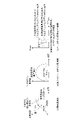
- FIG. 6 is a block diagram showing the configuration of optical sensor device 1001 according to the second embodiment.
- optical sensor device 1001 includes, in addition to the configuration of optical sensor device 1000 according to Embodiment 1, digital-to-analog converter 14 (second DAC) (second digital-to-analog converter), frequency phase It further comprises a comparator 15, a loop filter 16, and a second splitter 17 (brancher).
- second DAC digital-to-analog converter
- second splitter 17 brancher
- the second splitter 17 splits the internal received signal acquired by the optical heterodyne receiver 6 to the frequency phase comparator 15 and the analog-to-digital converter 7 .
- the internal reception signal here is obtained by combining the local light beam split by the optical splitter 2 and the internal reflection light reflected by the reference reflection point 4 by the optical heterodyne receiver 6. It is obtained as an electric signal by photoelectrically converting the waved light.
- the optical heterodyne receiver 6 acquires the internal received signal while blocking the reflected light from the object 999 to be measured.
- the analog-to-digital converter 7 samples the internal received signal branched by the second splitter 17 in synchronization with the second clock signal generated by the phase-locked loop 12 and converts it into a digital signal.
- the analog-to-digital converter 7 outputs the internally received signal converted into a digital signal to the signal processing device 9 .
- the signal processing device 9 further calculates second frequency variation reference signal data based on the internal received signal converted into a digital signal by the analog-to-digital converter 7 . More specifically, in the second embodiment, the signal processing device 9 synchronizes with the reference clock signal branched by the branching device 11, and based on the internal received signal converted into a digital signal by the analog-to-digital converter 7, 2 frequency variation reference signal data is further calculated. The signal processing device 9 outputs the calculated second frequency variation reference signal data to the digital-analog converter 14 (93 in FIG. 6). More specifically, in the second embodiment, the signal processing device 9 stores the calculated second frequency variation reference signal data in a memory (not shown), and the memory stores the stored second frequency variation reference signal data. to the digital-to-analog converter 14 .
- the second frequency variation reference signal data may be, for example, the internal received signal itself converted into a digital signal by the analog-to-digital converter 7 .
- the signal processing device 9 may calculate the second frequency variation reference signal data by removing unnecessary frequency components from the internal received signal converted into a digital signal by the analog-to-digital converter 7 .
- the digital-to-analog converter 14 converts the second frequency variation reference signal data calculated by the signal processing device 9 into an analog signal to generate a second frequency variation reference signal. More specifically, in the second embodiment, the digital-to-analog converter 14 converts the second frequency variation reference signal data calculated by the signal processing device 9 in synchronization with the second clock signal generated by the phase-locked loop 12. A second frequency varying reference signal is generated by converting to an analog signal. The digital-to-analog converter 14 outputs the generated second frequency variation reference signal to the frequency phase comparator 15 (141 in FIG. 1).
- the frequency phase comparator 15 generates a frequency error signal by comparing the internal received signal branched by the second splitter 17 and the second frequency fluctuation reference signal generated by the digital-to-analog converter 14 .
- the frequency phase comparator 15 outputs the generated error signal to the loop filter 16 .
- Loop filter 16 generates a control signal by integrating the error signal generated by frequency phase comparator 15 . Loop filter 16 outputs the generated control signal to wavelength swept light source 1 . The wavelength swept light source 1 adjusts the frequency of output light based on the control signal generated by the loop filter 16 .
- FIG. 7 is a graph for explaining a specific example of signal processing for internally reflected light by the optical sensor device 1001 according to the second embodiment.
- FIG. 7(a) shows an internal reception signal (difference beat B) acquired by the optical heterodyne receiver 6 combining local light and internal reflected light and photoelectrically exchanging the combined light in the specific example.
- 2 is a graph showing the time change (dotted line) of the frequency of (heterodyne frequency).
- the dashed line in FIG. 7(a) indicates the second frequency-varying reference signal generated by the digital-to-analog converter 14.
- the waveform of the swept wavelength light changes each time the swept wavelength light source 1 sweeps, so the curve that draws the instantaneous frequency of the difference beat B changes. Therefore, during a certain sweep, the frequency phase comparator 15 outputs the difference beat B, which is the internal received signal branched by the second splitter 17, and the second frequency fluctuation reference generated by the digital-to-analog converter 14, as described above. signal to generate a frequency error signal.
- Loop filter 16 generates a control signal by integrating the error signal generated by frequency phase comparator 15 .
- the wavelength swept light source 1 adjusts the frequency of the output light based on the control signal generated by the loop filter 16, so that the frequency and phase of the output wavelength swept light are the same as those of the second reflection point frequency fluctuation signal. Converge on frequency and phase. Such a converging operation improves the reproducibility of the nonlinearity of the wavelength-swept light.
- FIG. 7 is a graph showing the frequency spectrum (solid line) that is the result of fast Fourier transform of the internal reception signal by the signal processing device 9 in the specific example.
- the internal received signal here is derived from the wavelength swept light source 1 whose frequency is adjusted based on the control signal generated by the loop filter 16, and the optical heterodyne receiver 6 acquires the internal received signal, and analog
- the digital converter 7 performs sampling in synchronism with the above-described first frequency-fluctuation reference signal and converts it into a digital signal.
- the dotted line in FIG. 7B is the frequency spectrum when the analog-to-digital converter 7 samples the internal received signal in synchronization with the second clock signal of the phase-locked loop 12 and converts it into a digital signal. indicates Also, the dashed line in FIG. 7(b) indicates the frequency spectrum when the wavelength swept light source 1 does not adjust the frequency of the wavelength swept light.
- the wavelength swept light source 1 does not adjust the frequency of the wavelength swept light, the nonlinearity of the wavelength swept light whose waveform changes is not compensated for. spreads along the frequency axis.
- the wavelength-swept light source 1 adjusts the frequency of the wavelength-swept light as described above, the non-linearity of the wavelength-swept light whose waveform changes is compensated for, so that the solid line in FIG. , the spread of the spectrum of the difference beat B is suppressed.
- FIG. 8 is a graph for explaining a specific example of signal processing for reflected light by the photosensor device 1001 according to the second embodiment.
- FIG. 8(a) shows the frequency of the received signal (difference beat A) acquired by the optical heterodyne receiver 6 combining local light and reflected light and photoelectrically exchanging the combined light in the specific example.
- FIG. 10 is a graph showing a time change (dashed line) of (heterodyne frequency);
- FIG. The dotted line in (a) of FIG. 8 is a graph showing the change over time of the frequency of the difference beat A when the wavelength swept light source 1 does not adjust the frequency of the wavelength swept light.
- a dashed dotted line in FIG. 8(a) indicates the first frequency variation reference signal.
- the waveform of the swept wavelength light changes each time the swept wavelength light source 1 sweeps, so the curve representing the instantaneous frequency of the difference beat A changes. Therefore, by adjusting the frequency of the light output from the wavelength swept light source 1 by the means described above, the frequency and phase of the wavelength swept light are converged to the same frequency and phase as those of the second reflection point frequency fluctuation signal. As a result, the instantaneous frequency of the difference beat A also converges as indicated by the dashed line in FIG. 8(a), and the width of fluctuation for each sweep becomes smaller.
- FIG. 8 is a graph showing the frequency spectrum (the inner solid line) that is the result of fast Fourier transform of the received signal by the signal processing device 9 in the specific example.
- the received signal here is derived from the swept wavelength light whose frequency is adjusted by the swept wavelength light source 1 based on the control signal generated by the loop filter 16.
- 7 is a signal converted into a digital signal by sampling in synchronization with the first frequency-varying reference signal.
- the solid line outside FIG. 8(b) indicates the frequency when the analog-to-digital converter 7 samples the received signal in synchronization with the second clock signal of the phase-locked loop 12 described above and converts it into a digital signal.
- a spectrum is shown.
- the dashed line in FIG. 8(b) indicates the frequency spectrum when the wavelength swept light source 1 does not adjust the frequency of the wavelength swept light.
- the signal processing device 9 can calculate the position information of the measurement object based on the FFT bin number.
- the sensor resolution can be improved without using an additional interferometer for compensating for the nonlinearity of the wavelength swept light whose waveform changes.
- it is possible to suppress the drift of the measurement data due to the nonlinearity of the wavelength swept light due to environmental fluctuations and the change in the sweep frequency width. can be planned.
- Embodiment 3 a configuration for separating a received signal derived from the reflected light reflected by the measurement target 999 and an internal received signal derived from the internally reflected light reflected by the reference reflection point 4 will be described.
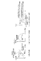
- FIG. 9 is a block diagram showing the configuration of optical sensor device 1002 according to the third embodiment.
- optical sensor device 1002 includes optical frequency shifter 18, shift frequency oscillator 19, third splitter 20, low-pass filter 201 ( 1st filter), a high-pass filter 202 (second filter), a doubler 203 and a frequency mixer 204 .
- An optical frequency shifter 18 is installed between the reference reflection point 4 and the optical sensor head 5 .
- a low-pass filter 201 is installed between the second splitter 17 and the frequency phase comparator 15 .
- a high-pass filter 202 and a frequency mixer 204 are installed between the second splitter 17 and the analog-to-digital converter 7 .
- the shift frequency oscillator 19 outputs a frequency shift signal for frequency shifting to the third splitter 20 .
- the third splitter 20 splits the frequency-shifted signal output from the shift frequency oscillator 19 to the optical frequency shifter 18 and the doubler 203 .
- the doubler 203 doubles the frequency-shifted signal split by the third splitter 20 .
- the doubler 203 outputs the doubled frequency-shifted signal to the frequency mixer 204 .
- the optical frequency shifter 18 frequency-shifts the signal light that has passed through the reference reflection point 4 . More specifically, in Embodiment 3, the optical frequency shifter 18 frequency-shifts the signal light that has passed through the reference reflection point 4 based on the frequency-shifted signal split by the third splitter 20 . More specifically, in Embodiment 3, the optical frequency shifter 18 downshifts the frequency of the signal light that has passed through the reference reflection point 4 . The optical frequency shifter 18 outputs the frequency-shifted (down-shifted) signal light to the optical sensor head 5 .
- an acousto-optic modulator can be used as the optical frequency shifter 18 .
- the waveform of the frequency shift signal output by the shift frequency oscillator 19 is a sine waveform.
- a LiNbO3 phase modulator that gives serrodyne modulation by applying a linear phase chirp to the signal light that has passed through the reference reflection point 4 can be used as the optical frequency shifter 18.
- the waveform of the frequency shift signal output from the shift frequency oscillator 19 is a sawtooth waveform that repeats linear voltage changes.
- the optical sensor head 5 emits the signal light frequency-shifted by the optical frequency shifter 18 toward the measurement target, and receives the reflected light reflected by the measurement target.
- the optical sensor head 5 outputs the received reflected light to the optical frequency shifter 18 .
- the optical frequency shifter 18 frequency-shifts the reflected light output from the optical sensor head 5 again.
- the optical frequency shifter 18 outputs the frequency-shifted reflected light to the optical heterodyne receiver 6 via the reference reflection point 4 and the optical circulator 3 .
- the optical heterodyne receiver 6 multiplexes the local light beam split by the optical splitter 2 and the reflected light output by the optical frequency shifter 18, and photoelectrically converts the multiplexed light into a received signal as an electrical signal. to get The optical heterodyne receiver 6 multiplexes the local light beam split by the optical splitter 2 and the internal reflected light reflected by the reference reflection point 4, and photoelectrically converts the combined light into an electric signal. Further obtain the internal received signal as .
- the second splitter 17 splits the received signal acquired by the optical heterodyne receiver 6 and the internal received signal to a low-pass filter 201 and a high-pass filter 202 .
- the low-pass filter 201 passes the internal reception signal branched by the second branching device 17 and blocks the reception signal branched by the second branching device 17 . That is, due to the downshifting by the optical frequency shifter 18 described above, the received signal, which is a beat signal based on the frequency difference between the reflected light and the local light, is changed to the internal received signal, which is a beat signal based on the frequency difference between the internally reflected light and the local light. Since the frequency is higher than the signal, it is cut off by the low-pass filter 201 .
- the high-pass filter 202 passes the received signal branched by the second branching device 17 and cuts off the internal received signal branched by the second branching device 17 . That is, due to the downshifting by the optical frequency shifter 18 described above, the received signal, which is a beat signal based on the frequency difference between the reflected light and the local light, is changed to the internal received signal, which is a beat signal based on the frequency difference between the internally reflected light and the local light. Since it has a higher frequency than the signal, it passes through the high pass filter 202 .
- the frequency phase comparator 15 generates a frequency error signal by comparing the internal received signal passed by the low-pass filter 201 and the second frequency fluctuation reference signal generated by the digital-to-analog converter 14 .
- the frequency mixer 204 frequency-shifts the received signal passed by the high-pass filter 202 by twice the amount of shift by the optical frequency shifter 18 . More specifically, in the third embodiment, frequency mixer 204 multiplies the received signal passed by high-pass filter 202 by the frequency-shifted signal doubled by doubler 203, thereby downgrading the received signal. shift. The frequency mixer 204 outputs the frequency-shifted (down-shifted) received signal to the analog-to-digital converter 7 .
- the analog-to-digital converter 7 samples the received signal passed by the high-pass filter 202 in synchronization with the first frequency variation reference signal generated in advance by the digital-to-analog converter 8 . More specifically, in the third embodiment, analog-to-digital converter 7 samples the received signal frequency-shifted by frequency mixer 204 in synchronization with the first frequency-fluctuation reference signal generated by digital-to-analog converter 8 .
- FIG. 10 is a graph for explaining a specific example of a method for separating a received signal and an internal received signal by the photosensor device 1002 according to the third embodiment.
- (a) of FIG. 10 shows the temporal change (dashed line) of the frequency of the local light branched by the optical splitter 2 and the temporal change (dotted line) of the frequency of the internally reflected light reflected by the reference reflection point 4 in the specific example. ) and the time change (solid line) of the frequency of the reflected light received by the optical sensor head 5 from the measurement object 999 and frequency-shifted again by the optical frequency shifter 18.
- FIG. 10 shows the temporal change (dashed line) of the frequency of the local light branched by the optical splitter 2 and the temporal change (dotted line) of the frequency of the internally reflected light reflected by the reference reflection point 4 in the specific example. ) and the time change (solid line) of the frequency of the reflected light received by the optical sensor head 5 from the measurement object 999 and frequency-shifted again by the optical
- the optical frequency shifter 18 shifts the frequency of the signal light that has passed through the reference reflection point 4 by f shift (corresponding to the frequency of the shift frequency oscillator 19), and the optical sensor head 5 receives it from the measurement object 999 by the amount of f shift .
- the frequency of the reflected light is down-shifted again.
- only the reflected light component of the light input to the optical heterodyne receiver 6 undergoes a 2f shift downshift, as shown in FIG. 10(a).
- FIG. 10(b) shows an internal received signal (difference beat B) acquired by the optical heterodyne receiver 6 combining local light and internal reflected light and photoelectrically exchanging the combined light in the specific example. and the received signal (difference beat A) acquired by the optical heterodyne receiver 6 combining local light and reflected light and photoelectrically exchanging the combined light.
- 10 is a graph showing a time change (solid line) of frequency (heterodyne frequency);
- the high-pass filter 202 can selectively extract the difference beat A between the local light and the reflected light reflected by the object to be measured.
- the differential beat B can be selectively extracted by the low-pass filter 201 .
- (c) of FIG. 10 shows the temporal change in the frequency of the received signal (difference beat A) input to the analog-to-digital converter 7 .
- (d) of FIG. 10 shows the time change of the frequency of the internal received signal (difference beat B) inputted to the frequency phase comparator 15 .
- the frequency mixer 204 down-converts the input received signal by a frequency that is twice the amount of shift by the optical frequency shifter 18 .
- the received signal is input to the analog-to-digital converter 7 with the shift component removed by the optical frequency shifter 18 .
- unnecessary reception signal components derived from reflected light from the object to be measured are removed from the signal input to the frequency phase comparator 15. It is possible to improve the convergence accuracy of the wavelength swept light and improve the resolution of the position measurement of the measurement object.
- the signal processing device 9 when calculating the measurement data for the measurement object 999 based on the received signal converted into a digital signal by the analog-to-digital converter 7, corrects the nonlinearity of the received signal caused by the frequency shift by the optical frequency shifter 18. You can compensate for gender.
- Embodiment 4 In the second embodiment, a configuration has been described in which the swept wavelength light source 1 adjusts the frequency of the swept wavelength light to compensate for the nonlinearity of the swept wavelength light whose waveform changes. In the fourth embodiment, a configuration for compensating for the nonlinearity of the wavelength swept light whose waveform changes by frequency-shifting the local light split by the optical splitter 2 will be described.
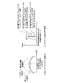
- FIG. 11 is a block diagram showing the configuration of optical sensor device 1003 according to the fourth embodiment. As shown in FIG. 11, optical sensor device 1003 further includes optical frequency shifter 18, frequency mixer 204, and voltage controlled oscillator 205 in addition to the configuration of optical sensor device 1001 according to the second embodiment.
- the loop filter 16 according to Embodiment 4 generates a control signal by integrating the error signal generated by the frequency phase comparator 15 and outputs the generated control signal to the voltage controlled oscillator 205 .
- a voltage controlled oscillator 205 generates a control signal for the optical frequency shifter 18 based on the control signal generated by the loop filter 16 .
- the voltage controlled oscillator 205 outputs the generated control signal to the optical frequency shifter 18 .
- the optical frequency shifter 18 frequency-shifts the local oscillator light split by the optical splitter 2 based on the control signal generated by the voltage-controlled oscillator 205 .
- the optical frequency shifter 18 outputs the frequency-shifted local light to the optical heterodyne receiver 6 .
- the optical heterodyne receiver 6 multiplexes the local light frequency-shifted by the optical frequency shifter 18 and the internally reflected light of the signal light split by the optical splitter 2, and converts the combined light into a photoelectric converter. Obtain the internal received signal by transforming it. More specifically, in the fourth embodiment, the optical heterodyne receiver 6 multiplexes the local light frequency-shifted by the optical frequency shifter 18 and the internally reflected light reflected by the reference reflection point 4, and multiplexes An internal reception signal is obtained by photoelectrically converting the light.
- the optical heterodyne receiver 6 When the optical sensor device 1003 measures measurement data on the object 999 to be measured, the optical heterodyne receiver 6 multiplexes the local light frequency-shifted by the optical frequency shifter 18 and the reflected light received by the optical sensor head 5 . Then, the received signal is obtained by photoelectrically converting the combined light.
- the frequency mixer 204 frequency-shifts the internal received signal split by the second splitter 17 .
- the frequency mixer 204 frequency-shifts the received signal split by the second splitter 17 . More specifically, frequency mixer 204 frequency shifts the internal received signal and the received signal, respectively, in synchronization with the second clock signal (124 in FIG. 11) generated by phase locked loop 12 . A detailed configuration of the frequency mixer 204 will be described later.
- FIG. 12 shows the frequency (heterodyne Fig. 10 is a graph showing a time change (dotted line) of frequency).
- a dashed line in FIG. 12 indicates the second frequency-varying reference signal generated by the digital-to-analog converter 14 .
- the optical frequency shifter 18 frequency-shifts the local light branched by the optical branching device 2 by the instantaneous frequency f vco (t) based on the control signal generated by the voltage controlled oscillator 205 .
- the instantaneous heterodyne frequency of the internal received signal (difference beat B) acquired by the optical heterodyne receiver 6 at a certain sweep time X is f bX (t)+f vco ( t).
- f bX (t) is the frequency of the difference beat B at a sweep time X;
- the signal processing device 9 calculates the second frequency variation reference signal data by giving an offset to the frequency of the internal received signal converted into a digital signal by the analog-to-digital converter 7 . More specifically, in this specific example, the signal processing device 9 applies an offset f offset to the frequency of the internal received signal converted into a digital signal by the analog-to-digital converter 7, thereby increasing the frequency as indicated by the dashed line in FIG. calculates f ref (t)+f offset second frequency variation reference signal data.
- the frequency mixer 204 When measuring the measurement data for the measurement target 999, the frequency mixer 204 downshifts the frequency of the received signal branched by the second splitter 17 by the offset f offset .
- Analog-to-digital converter 7 samples the received signal down-shifted by frequency mixer 204 in synchronization with the first frequency-fluctuation reference signal generated by digital-to-analog converter 8 .
- the comparison frequency in the frequency phase comparator 15 can be increased by the amount of the offset, so that the operation is stabilized and highly accurate measurement data can be obtained.
- frequency-shifting the local light it is possible to compensate for the nonlinearity of the wavelength-swept light whose waveform changes, so it is possible to use a wavelength-swept light source whose wavelength sweep cannot be controlled externally, improving design flexibility.
- the function of the signal processing device 9 of the optical sensor device 1000, the optical sensor device 1001, the optical sensor device 1002, or the optical sensor device 1003 is realized by a processing circuit. That is, the signal processing device 9 includes a processing circuit for executing the above processing. This processing circuit may be dedicated hardware, or may be a CPU (Central Processing Unit) that executes a program stored in memory.
- CPU Central Processing Unit
- FIG. 13A is a block diagram showing a hardware configuration that implements the functions of the signal processing device 9 of the optical sensor device 1000, the optical sensor device 1001, the optical sensor device 1002, or the optical sensor device 1003.
- FIG. 13B is a block diagram showing a hardware configuration for executing software that realizes the functions of the signal processing device 9 of the optical sensor device 1000, the optical sensor device 1001, the optical sensor device 1002, or the optical sensor device 1003.
- FIG. 13A is a block diagram showing a hardware configuration that implements the functions of the signal processing device 9 of the optical sensor device 1000, the optical sensor device 1001, the optical sensor device 1002, or the optical sensor device 1003.
- FIG. 13B is a block diagram showing a hardware configuration for executing software that realizes the functions of the signal processing device 9 of the optical sensor device 1000, the optical sensor device 1001, the optical sensor device 1002, or the optical sensor device 1003.
- processing circuit is the dedicated hardware processing circuit 300 shown in FIG. Circuit), FPGA (Field-Programmable Gate Array), or a combination thereof.
- the functions of the signal processing device 9 of the optical sensor device 1000, the optical sensor device 1001, the optical sensor device 1002, or the optical sensor device 1003 may be realized by separate processing circuits, or these functions may be integrated into one processing circuit. may be realized.
- the processing circuit is the processor 301 shown in FIG. 13B
- the function of the signal processing device 9 of the optical sensor device 1000, the optical sensor device 1001, the optical sensor device 1002, or the optical sensor device 1003 is software, firmware, or software and firmware. realized by a combination of Software or firmware is written as a program and stored in the memory 302 .
- the processor 301 reads and executes a program stored in the memory 302 to realize the function of the signal processing device 9 of the optical sensor device 1000, the optical sensor device 1001, the optical sensor device 1002, or the optical sensor device 1003. That is, the signal processing device 9 of the optical sensor device 1000, the optical sensor device 1001, the optical sensor device 1002, or the signal processing device 9 of the optical sensor device 1003 executes the above-described processing as a result when these functions are executed by the processor 301.
- a memory 302 for storing a program to be executed;
- the memory 302 may be a computer-readable storage medium storing a program for causing a computer to function as the signal processing device 9 of the optical sensor device 1000, the optical sensor device 1001, the optical sensor device 1002, or the optical sensor device 1003. .
- the processor 301 corresponds to, for example, a CPU (Central Processing Unit), a processing device, an arithmetic device, a processor, a microprocessor, a microcomputer, or a DSP (Digital Signal Processor).
- a CPU Central Processing Unit
- a processing device for example, a CPU (Central Processing Unit), a processing device, an arithmetic device, a processor, a microprocessor, a microcomputer, or a DSP (Digital Signal Processor).
- DSP Digital Signal Processor
- the memory 302 includes, for example, non-volatile or volatile semiconductor memories such as RAM (Random Access Memory), ROM (Read Only Memory), flash memory, EPROM (Erasable Programmable Read Only Memory), EEPROM (Electrically-EPROM), Magnetic discs such as hard disks and flexible discs, flexible discs, optical discs, compact discs, mini discs, DVDs (Digital Versatile Discs) and the like are applicable.
- RAM Random Access Memory
- ROM Read Only Memory
- flash memory EPROM (Erasable Programmable Read Only Memory)
- EEPROM Electrically-EPROM
- Magnetic discs such as hard disks and flexible discs, flexible discs, optical discs, compact discs, mini discs, DVDs (Digital Versatile Discs) and the like are applicable.
- the functions of the signal processing device 9 of the optical sensor device 1000, the optical sensor device 1001, the optical sensor device 1002, or the optical sensor device 1003 may be partly realized by dedicated hardware and partly realized by software or firmware. .
- the processing circuitry may implement each of the above functions in hardware, software, firmware, or a combination thereof. It should be noted that it is possible to freely combine each embodiment, modify any component of each embodiment, or omit any component from each embodiment.
- the optical sensor device can reduce the signal processing load caused by compensating for the nonlinearity of the wavelength swept light, it can be used as a technique for compensating for the nonlinearity of the wavelength swept light.
- 1 wavelength swept light source 1 wavelength swept light source, 2 optical splitter, 3 optical circulator, 4 reference reflection point, 5 optical sensor head, 6 optical heterodyne receiver, 7 analog-to-digital converter, 8 digital-to-analog converter, 9 signal processor, 10 reference clock, 11 branching device, 12 phase-locked loop, 13 switch, 14 digital-to-analog converter, 15 frequency phase comparator, 16 loop filter, 17 second branching device, 18 optical frequency shifter, 19 shift frequency oscillator, 20 third branching device, 201 low-pass filter, 202 high-pass filter, 203 doubler, 204 frequency mixer, 205 voltage controlled oscillator, 300 processing circuit, 301 processor, 302 memory, 999 measurement object, 1000, 1001, 1002, 1003 photosensor device.
Landscapes
- Physics & Mathematics (AREA)
- General Physics & Mathematics (AREA)
- Engineering & Computer Science (AREA)
- Electromagnetism (AREA)
- Remote Sensing (AREA)
- Radar, Positioning & Navigation (AREA)
- Computer Networks & Wireless Communication (AREA)
- Biochemistry (AREA)
- Health & Medical Sciences (AREA)
- Pathology (AREA)
- General Health & Medical Sciences (AREA)
- Analytical Chemistry (AREA)
- Chemical & Material Sciences (AREA)
- Life Sciences & Earth Sciences (AREA)
- Immunology (AREA)
- Investigating Or Analysing Materials By Optical Means (AREA)
- Photometry And Measurement Of Optical Pulse Characteristics (AREA)
- Optical Communication System (AREA)
- Optical Transform (AREA)
- Optical Radar Systems And Details Thereof (AREA)
- Length Measuring Devices By Optical Means (AREA)
Abstract
Description
本開示は、上記のような問題点を解決するためになされたものであり、波長掃引光の非線形性を補償することによって生じる信号処理負荷を軽減させる技術を提供する。
実施の形態1.
図1は、実施の形態1に係る光センサ装置1000の構成を示すブロック図である。図1が示すように、光センサ装置1000は、波長掃引光源1、光分岐器2、光サーキュレータ3、参照反射点4、光センサヘッド5、光ヘテロダイン受信器6、アナログデジタルコンバータ7(ADC)、デジタルアナログコンバータ8(DAC)(第1のデジタルアナログコンバータ)、信号処理装置9、基準クロック10、分岐器11、フェーズロックドループ12(PLL)、及びスイッチ13を備えている。
光サーキュレータ3は、光分岐器2が分岐させた信号光を参照反射点4に出力する。
まずは、測定対象999から反射された反射光を遮断した状態で、光ヘテロダイン受信器6は、光分岐器2が分岐させた局発光と、参照反射点4によって反射された内部反射光とを合波し、合波した光を光電変換することにより電気信号としての内部受信信号を取得する。アナログデジタルコンバータ7は、スイッチ13が切り替えた第2のクロック信号(フェーズロックドループ12が生成した第2のクロック信号)に同期して、光ヘテロダイン受信器6が取得した内部受信信号をサンプリングすることによりデジタル信号に変換する。
当該具体例では、信号処理装置9は、アナログデジタルコンバータ7がデジタル信号に変換した内部受信信号及び受信信号に対してそれぞれ高速フーリエ変換(FFT)を行う。
実施の形態1では、波長掃引光源1が出力する波長掃引光の波形が変化しない構成について説明した。しかし、波長掃引光の波形が変化する場合、測定対象の位置測定の分解能が低下してしまう。そこで、実施の形態2では、波形が変化する波長掃引光の非線形性を補償する構成について説明する。
波長掃引光源1は、ループフィルタ16が生成した制御信号に基づいて、出力する光の周波数を調整する。
実施の形態3では、測定対象999によって反射された反射光に由来する受信信号と、参照反射点4によって反射された内部反射光に由来する内部受信信号とを分離する構成について説明する。
第3の分岐器20は、シフト周波数発振器19が出力した周波数シフト信号を、光周波数シフタ18と2逓倍器203とに分岐させる。
2逓倍器203は、第3の分岐器20が分岐させた周波数シフト信号を2逓倍する。2逓倍器203は、2逓倍した周波数シフト信号を周波数ミキサ204に出力する。
ローパスフィルタ201は、第2の分岐器17が分岐させた内部受信信号を通過させ、第2の分岐器17が分岐させた受信信号を遮断する。つまり、上述の光周波数シフタ18によるダウンシフトによって、反射光と局発光との周波数差に基づくビート信号である受信信号は、内部反射光と局発光との周波数差に基づくビート信号である内部受信信号よりも周波数が高くなるため、ローパスフィルタ201によって遮断される。
実施の形態2では、波長掃引光源1が波長掃引光の周波数を調整することにより、波形が変化する波長掃引光の非線形性を補償する構成について説明した。実施の形態4では、光分岐器2が分岐させた局発光を周波数シフトさせることにより、波形が変化する波長掃引光の非線形性を補償する構成について説明する。
なお、ソフトウェア又はファームウェアは、プログラムとして記述されてメモリ302に記憶される。
なお、各実施の形態の自由な組み合わせ、あるいは各実施の形態の任意の構成要素の変形、もしくは各実施の形態において任意の構成要素の省略が可能である。
Claims (11)
- 時間の経過とともに周波数が変化する光を出力する波長掃引光源と、
前記波長掃引光源が出力した光を信号光及び局発光に分岐させる光分岐器と、
前記光分岐器が分岐させた信号光を測定対象に向かって出射し、当該測定対象によって反射された反射光を受信する光センサヘッドと、
前記光分岐器が分岐させた局発光、及び前記光センサヘッドが受信した反射光を合波し、合波した光を光電変換することにより電気信号としての受信信号を取得する光ヘテロダイン受信器と、
前記光ヘテロダイン受信器が取得した受信信号をサンプリングすることによりデジタル信号に変換するアナログデジタルコンバータと、
前記アナログデジタルコンバータの第1のクロック信号を生成する第1のデジタルアナログコンバータと、
前記アナログデジタルコンバータがデジタル信号に変換した受信信号に基づいて、前記測定対象に関する測定データを算出する信号処理装置と、を備え、
前記光ヘテロダイン受信器は、前記光分岐器が分岐させた局発光と、前記光分岐器が分岐させた信号光が内部反射された内部反射光とを合波し、合波した光を光電変換することにより電気信号としての内部受信信号をさらに取得し、
前記アナログデジタルコンバータは、前記光ヘテロダイン受信器が取得した内部受信信号をサンプリングすることによりデジタル信号にさらに変換し、
前記信号処理装置は、前記アナログデジタルコンバータがデジタル信号に変換した内部受信信号に基づいて、前記波長掃引光源が出力した光の周波数変動に対する基準となる第1の周波数変動基準信号データをさらに算出し、
前記第1のデジタルアナログコンバータは、前記信号処理装置が算出した第1の周波数変動基準信号データをアナログ信号に変換することにより、前記第1のクロック信号として第1の周波数変動基準信号を生成し、
前記アナログデジタルコンバータは、前記第1のデジタルアナログコンバータが生成した第1の周波数変動基準信号に同期して、前記光ヘテロダイン受信器が取得した受信信号をサンプリングすることを特徴とする、光センサ装置。 - 前記光分岐器が分岐させた信号光を部分的に反射することにより内部反射する参照反射点をさらに備え、
前記光ヘテロダイン受信器は、前記光分岐器が分岐させた局発光と、前記参照反射点によって反射された内部反射光とを合波し、合波した光を光電変換することにより電気信号としての内部受信信号をさらに取得することを特徴とする、請求項1に記載の光センサ装置。 - 前記アナログデジタルコンバータの第2のクロック信号を生成するフェーズロックドループをさらに備え、
前記アナログデジタルコンバータは、前記フェーズロックドループが生成した第2のクロック信号に同期して、前記光ヘテロダイン受信器が取得した内部受信信号をサンプリングすることを特徴とする、請求項1に記載の光センサ装置。 - 前記アナログデジタルコンバータのクロック信号を、前記第1のデジタルアナログコンバータが生成した第1のクロック信号としての第1の周波数変動基準信号、又は前記フェーズロックドループが生成した第2のクロック信号の何れか一方に切り替えるスイッチをさらに備えていることを特徴とする、請求項3に記載の光センサ装置。
- 前記信号処理装置は、前記アナログデジタルコンバータがデジタル信号に変換した内部受信信号をヒルベルト変換することにより、当該内部受信信号の瞬時周波数を算出し、算出した瞬時周波数を逓倍することにより、前記第1の周波数変動基準信号データを算出することを特徴とする、請求項1に記載の光センサ装置。
- 分岐器、第2のデジタルアナログコンバータ、周波数位相比較器、及びループフィルタをさらに備え、
前記分岐器は、前記光ヘテロダイン受信器が取得した内部受信信号を、前記周波数位相比較器と前記アナログデジタルコンバータとに分岐させ、
前記信号処理装置は、前記アナログデジタルコンバータがデジタル信号に変換した内部受信信号に基づいて、第2の周波数変動基準信号データをさらに算出し、
前記第2のデジタルアナログコンバータは、前記信号処理装置が算出した第2の周波数変動基準信号データをアナログ信号に変換することにより、第2の周波数変動基準信号を生成し、
前記周波数位相比較器は、前記分岐器が分岐した内部受信信号と、前記第2のデジタルアナログコンバータが生成した第2の周波数変動基準信号とを比較することにより、周波数の誤差信号を生成し、
前記ループフィルタは、前記周波数位相比較器が生成した誤差信号を積分することにより制御信号を生成し、
前記波長掃引光源は、前記ループフィルタが生成した制御信号に基づいて、出力する光の周波数を調整することを特徴とする、請求項1に記載の光センサ装置。 - 参照反射点、光周波数シフタ、第1のフィルタ、及び第2のフィルタをさらに備え、
前記参照反射点は、前記光分岐器が分岐させた信号光を部分的に反射することにより内部反射し、
前記光周波数シフタは、前記参照反射点を通過した信号光を周波数シフトさせ、
前記光センサヘッドは、前記光周波数シフタが周波数シフトさせた信号光を前記測定対象に向かって出射し、当該測定対象によって反射された反射光を受信し、
前記光ヘテロダイン受信器は、前記光分岐器が分岐させた局発光と、前記参照反射点によって反射された内部反射光とを合波し、合波した光を光電変換することにより電気信号としての内部受信信号をさらに取得し、
前記分岐器は、前記光ヘテロダイン受信器が取得した受信信号及び内部受信信号を、前記第1のフィルタと前記第2のフィルタとに分岐させ、
前記第1のフィルタは、前記分岐器が分岐させた内部受信信号を通過させ、前記分岐器が分岐させた受信信号を遮断し、
前記第2のフィルタは、前記分岐器が分岐させた受信信号を通過させ、前記分岐器が分岐させた内部受信信号を遮断し、
前記周波数位相比較器は、前記第1のフィルタが通過させた内部受信信号と、前記第2のデジタルアナログコンバータが生成した第2の周波数変動基準信号とを比較することにより、周波数の誤差信号を生成し、
前記アナログデジタルコンバータは、前記第1のデジタルアナログコンバータが生成した第1の周波数変動基準信号に同期して、前記第2のフィルタが通過させた受信信号をサンプリングすることを特徴とする、請求項6に記載の光センサ装置。 - 周波数ミキサをさらに備え、
前記光周波数シフタは、前記光センサヘッドが受信した反射光をさらに周波数シフトさせ、
前記周波数ミキサは、前記光周波数シフタによるシフト量の2倍の周波数分、前記第2のフィルタが通過させた受信信号を周波数シフトさせ、
前記アナログデジタルコンバータは、前記第1のデジタルアナログコンバータが生成した第1の周波数変動基準信号に同期して、前記周波数ミキサが周波数シフトさせた受信信号をサンプリングすることを特徴とする、請求項7に記載の光センサ装置。 - 前記信号処理装置は、前記アナログデジタルコンバータがデジタル信号に変換した受信信号に基づいて、前記測定対象に関する測定データを算出する際に、前記光周波数シフタによる周波数シフトによって生じた受信信号の非線形性を補償することを特徴とする、請求項7に記載の光センサ装置。
- 分岐器、第2のデジタルアナログコンバータ、周波数位相比較器、ループフィルタ、電圧制御発振器、及び光周波数シフタをさらに備え、
前記分岐器は、前記光ヘテロダイン受信器が取得した内部受信信号を、前記周波数位相比較器と前記アナログデジタルコンバータとに分岐させ、
前記信号処理装置は、前記アナログデジタルコンバータがデジタル信号に変換した内部受信信号に基づいて、第2の周波数変動基準信号データをさらに算出し、
前記第2のデジタルアナログコンバータは、前記信号処理装置が算出した第2の周波数変動基準信号データをアナログ信号に変換することにより、第2の周波数変動基準信号を生成し、
前記周波数位相比較器は、前記分岐器が分岐した内部受信信号と、前記第2のデジタルアナログコンバータが生成した第2の周波数変動基準信号とを比較することにより、周波数の誤差信号を生成し、
前記ループフィルタは、前記周波数位相比較器が生成した誤差信号を積分することにより制御信号を生成し、
前記電圧制御発振器は、前記ループフィルタが生成した制御信号に基づいて、前記光周波数シフタの制御信号を発生させ、
前記光周波数シフタは、前記電圧制御発振器が発生させた制御信号に基づいて、前記光分岐器が分岐させた局発光を周波数シフトさせ、
前記光ヘテロダイン受信器は、前記光周波数シフタが周波数シフトさせた局発光と、前記光分岐器が分岐させた信号光が内部反射された内部反射光とを合波し、合波した光を光電変換することにより前記内部受信信号を取得し、前記光周波数シフタが周波数シフトさせた局発光と、前記光センサヘッドが受信した反射光とを合波し、合波した光を光電変換することにより前記受信信号を取得することを特徴とする、請求項1に記載の光センサ装置。 - 周波数ミキサをさらに備え、
前記信号処理装置は、前記アナログデジタルコンバータがデジタル信号に変換した内部受信信号の周波数にオフセットを与えることにより、前記第2の周波数変動基準信号データを算出し、
前記周波数ミキサは、前記分岐器が分岐させた受信信号及び内部受信信号の各周波数を、前記オフセットの分、ダウンシフトさせることを特徴とする、請求項10に記載の光センサ装置。
Priority Applications (6)
| Application Number | Priority Date | Filing Date | Title |
|---|---|---|---|
| CN202180099312.0A CN117460946A (zh) | 2021-06-18 | 2021-06-18 | 光传感器装置 |
| GB2318421.1A GB2622968B (en) | 2021-06-18 | 2021-06-18 | Optical sensor device |
| JP2023528906A JP7350217B2 (ja) | 2021-06-18 | 2021-06-18 | 光センサ装置 |
| PCT/JP2021/023157 WO2022264393A1 (ja) | 2021-06-18 | 2021-06-18 | 光センサ装置 |
| KR1020237042946A KR102650419B1 (ko) | 2021-06-18 | 2021-06-18 | 광 센서 장치 |
| US18/379,584 US20240053256A1 (en) | 2021-06-18 | 2023-10-12 | Optical sensor device |
Applications Claiming Priority (1)
| Application Number | Priority Date | Filing Date | Title |
|---|---|---|---|
| PCT/JP2021/023157 WO2022264393A1 (ja) | 2021-06-18 | 2021-06-18 | 光センサ装置 |
Related Child Applications (1)
| Application Number | Title | Priority Date | Filing Date |
|---|---|---|---|
| US18/379,584 Continuation US20240053256A1 (en) | 2021-06-18 | 2023-10-12 | Optical sensor device |
Publications (1)
| Publication Number | Publication Date |
|---|---|
| WO2022264393A1 true WO2022264393A1 (ja) | 2022-12-22 |
Family
ID=84526977
Family Applications (1)
| Application Number | Title | Priority Date | Filing Date |
|---|---|---|---|
| PCT/JP2021/023157 Ceased WO2022264393A1 (ja) | 2021-06-18 | 2021-06-18 | 光センサ装置 |
Country Status (6)
| Country | Link |
|---|---|
| US (1) | US20240053256A1 (ja) |
| JP (1) | JP7350217B2 (ja) |
| KR (1) | KR102650419B1 (ja) |
| CN (1) | CN117460946A (ja) |
| GB (1) | GB2622968B (ja) |
| WO (1) | WO2022264393A1 (ja) |
Cited By (2)
| Publication number | Priority date | Publication date | Assignee | Title |
|---|---|---|---|---|
| WO2025013662A1 (ja) * | 2023-07-11 | 2025-01-16 | テルモ株式会社 | 光干渉断層像形成装置 |
| WO2026038383A1 (ja) * | 2024-08-14 | 2026-02-19 | 三菱電機株式会社 | 光干渉距離測定装置 |
Citations (5)
| Publication number | Priority date | Publication date | Assignee | Title |
|---|---|---|---|---|
| US20140268038A1 (en) * | 2013-03-12 | 2014-09-18 | Carl Zeiss Meditec, Inc. | Systems and methods for variable depth optical coherence tomography imaging |
| JP2014533837A (ja) * | 2011-12-21 | 2014-12-15 | ウェイブライト ゲーエムベーハー | 掃引光源光干渉断層撮影のための装置及び方法 |
| JP2015099078A (ja) * | 2013-11-19 | 2015-05-28 | 株式会社トーメーコーポレーション | 光断層画像撮影装置 |
| JP2016031294A (ja) * | 2014-07-29 | 2016-03-07 | 日本電信電話株式会社 | 光干渉断層装置 |
| JP2016148539A (ja) * | 2015-02-10 | 2016-08-18 | アンリツ株式会社 | Oct装置 |
Family Cites Families (14)
| Publication number | Priority date | Publication date | Assignee | Title |
|---|---|---|---|---|
| EP1889037A2 (en) | 2005-06-01 | 2008-02-20 | The General Hospital Corporation | Apparatus, method and system for performing phase-resolved optical frequency domain imaging |
| JP4999147B2 (ja) * | 2006-05-22 | 2012-08-15 | 富士フイルム株式会社 | 波長掃引光源および光断層画像化装置 |
| WO2012100213A2 (en) * | 2011-01-21 | 2012-07-26 | Duke University | Systems and methods for complex conjugate artifact resolved optical coherence tomography |
| US8908189B2 (en) * | 2011-04-15 | 2014-12-09 | Carl Zeiss Meditec, Inc. | Systems and methods for swept-source optical coherence tomography |
| EP2574273B1 (en) * | 2011-06-23 | 2014-09-24 | Nidek Co., Ltd. | Optical coherence tomography apparatus |
| US9191020B2 (en) * | 2014-02-05 | 2015-11-17 | Waveworks, Inc. | Traveling-wave based high-speed sampling systems |
| JP2016090280A (ja) * | 2014-10-30 | 2016-05-23 | 日本電信電話株式会社 | 光断層画像撮像装置及びこれを使用した撮像方法 |
| JP6696782B2 (ja) | 2015-03-09 | 2020-05-20 | 炭 親良 | ビームフォーミング方法、計測イメージング装置、及び、通信装置 |
| US11255663B2 (en) * | 2016-03-04 | 2022-02-22 | May Patents Ltd. | Method and apparatus for cooperative usage of multiple distance meters |
| EP3743679B1 (en) | 2018-01-23 | 2023-06-28 | AMO Development, LLC | Methods and systems of optical coherence tomography with fiducial signal for correcting scanning laser nonlinearity |
| US20220244035A1 (en) * | 2019-07-18 | 2022-08-04 | Nippon Telegraph And Telephone Corporation | Wavelength Sweeping Optical Measurement System |
| JP7348582B2 (ja) * | 2020-09-09 | 2023-09-21 | 日本電信電話株式会社 | 光送信器及び光送信における周波数制御方法 |
| US11988903B2 (en) * | 2021-02-11 | 2024-05-21 | Raytheon Company | Photonic integrated circuit-based optical phased array calibration technique |
| KR102680481B1 (ko) * | 2021-04-06 | 2024-07-01 | 미쓰비시덴키 가부시키가이샤 | 광 측정 장치 |
-
2021
- 2021-06-18 KR KR1020237042946A patent/KR102650419B1/ko active Active
- 2021-06-18 GB GB2318421.1A patent/GB2622968B/en active Active
- 2021-06-18 JP JP2023528906A patent/JP7350217B2/ja active Active
- 2021-06-18 WO PCT/JP2021/023157 patent/WO2022264393A1/ja not_active Ceased
- 2021-06-18 CN CN202180099312.0A patent/CN117460946A/zh active Pending
-
2023
- 2023-10-12 US US18/379,584 patent/US20240053256A1/en active Pending
Patent Citations (5)
| Publication number | Priority date | Publication date | Assignee | Title |
|---|---|---|---|---|
| JP2014533837A (ja) * | 2011-12-21 | 2014-12-15 | ウェイブライト ゲーエムベーハー | 掃引光源光干渉断層撮影のための装置及び方法 |
| US20140268038A1 (en) * | 2013-03-12 | 2014-09-18 | Carl Zeiss Meditec, Inc. | Systems and methods for variable depth optical coherence tomography imaging |
| JP2015099078A (ja) * | 2013-11-19 | 2015-05-28 | 株式会社トーメーコーポレーション | 光断層画像撮影装置 |
| JP2016031294A (ja) * | 2014-07-29 | 2016-03-07 | 日本電信電話株式会社 | 光干渉断層装置 |
| JP2016148539A (ja) * | 2015-02-10 | 2016-08-18 | アンリツ株式会社 | Oct装置 |
Non-Patent Citations (2)
| Title |
|---|
| JIA, PINGPING ET AL.: "NON-DESTRUCTIVE AND REAL-TIME OPTICAL INSPECTION FOR LENS SIZE USING SWEPT SOURCE OPTICAL COHERENCE TOMOGRAPHY", PROCEEIDINGS OF SPIE. OPTICAL MEASUREMENT SYSTEMS FOR INDUSTRIAL INSPECTION XI., vol. 11056, 21 June 2019 (2019-06-21), pages 1 - 6, XP060122753, DOI: 10.1117/12.2525974 * |
| YAMAUCHI ET AL.: "A Study on Compensation Scheme of Wavelength Variations for SS-OCT Based Digital Photonics Sensor", PROCEEDINGS OF THE 2020 IEICE GENERAL CONFERENCE, March 2020 (2020-03-01) * |
Cited By (2)
| Publication number | Priority date | Publication date | Assignee | Title |
|---|---|---|---|---|
| WO2025013662A1 (ja) * | 2023-07-11 | 2025-01-16 | テルモ株式会社 | 光干渉断層像形成装置 |
| WO2026038383A1 (ja) * | 2024-08-14 | 2026-02-19 | 三菱電機株式会社 | 光干渉距離測定装置 |
Also Published As
| Publication number | Publication date |
|---|---|
| GB202318421D0 (en) | 2024-01-17 |
| CN117460946A (zh) | 2024-01-26 |
| KR20230173739A (ko) | 2023-12-27 |
| JPWO2022264393A1 (ja) | 2022-12-22 |
| US20240053256A1 (en) | 2024-02-15 |
| JP7350217B2 (ja) | 2023-09-25 |
| GB2622968A (en) | 2024-04-03 |
| GB2622968B (en) | 2024-11-06 |
| KR102650419B1 (ko) | 2024-03-21 |
Similar Documents
| Publication | Publication Date | Title |
|---|---|---|
| US12510639B2 (en) | System and method for increasing coherence length in lidar systems | |
| US20240053256A1 (en) | Optical sensor device | |
| US8699013B2 (en) | Chromatic dispersion measurement device and chromatic dispersion measurement method for measuring the dispersion of light pulses | |
| JP2014202716A (ja) | 距離測定装置 | |
| WO2019166876A1 (en) | Method and device for interferometric range measurements | |
| JP2010515919A5 (ja) | ||
| JP2019045200A (ja) | 光学的距離測定装置および測定方法 | |
| JP7010304B2 (ja) | 測距装置及び制御方法 | |
| US20200209392A1 (en) | Multi frequency long range distance detection for amplitude modulated continuous wave time of flight cameras | |
| WO2017014098A1 (ja) | ガス検知装置およびガス検知方法 | |
| JP7627487B2 (ja) | ライダー装置及びライダー制御方法 | |
| JP2000111312A (ja) | 光周波数線形掃引装置及び光周波数線形掃引装置のための変調補正デ―タ記録装置 | |
| CN113758412B (zh) | Oct测量装置以及oct测量方法 | |
| JP6991034B2 (ja) | 光波距離計及びフィードバック信号の変調周波数決定方法 | |
| US20140268290A1 (en) | System and method for increasing coherence length in lidar systems | |
| WO2019186776A1 (ja) | 測距装置及び制御方法 | |
| JP7564293B1 (ja) | 位相特性校正装置および位相特性校正方法 | |
| JP5480507B2 (ja) | レーザ干渉計 | |
| US7492464B2 (en) | Triggering for a heterodyne interferometer | |
| JP2020008357A (ja) | 距離計及び距離測定方法並びに光学的三次元形状測定機 | |
| CN118259268A (zh) | 光源线性度检测、线性调频控制方法、系统及激光雷达 | |
| JP7693147B1 (ja) | 波長分散補償装置、光測距装置および波長分散補償方法 | |
| EP4495629A1 (en) | Measurement apparatus and measurement method |
Legal Events
| Date | Code | Title | Description |
|---|---|---|---|
| 121 | Ep: the epo has been informed by wipo that ep was designated in this application |
Ref document number: 21946068 Country of ref document: EP Kind code of ref document: A1 |
|
| ENP | Entry into the national phase |
Ref document number: 2023528906 Country of ref document: JP Kind code of ref document: A |
|
| ENP | Entry into the national phase |
Ref document number: 202318421 Country of ref document: GB Kind code of ref document: A Free format text: PCT FILING DATE = 20210618 |
|
| WWE | Wipo information: entry into national phase |
Ref document number: 2318421.1 Country of ref document: GB |
|
| ENP | Entry into the national phase |
Ref document number: 20237042946 Country of ref document: KR Kind code of ref document: A |
|
| WWE | Wipo information: entry into national phase |
Ref document number: 202180099312.0 Country of ref document: CN Ref document number: 1020237042946 Country of ref document: KR |
|
| NENP | Non-entry into the national phase |
Ref country code: DE |
|
| WWP | Wipo information: published in national office |
Ref document number: 2318421.1 Country of ref document: GB |
|
| 122 | Ep: pct application non-entry in european phase |
Ref document number: 21946068 Country of ref document: EP Kind code of ref document: A1 |
|
| WWG | Wipo information: grant in national office |
Ref document number: 2318421.1 Country of ref document: GB |