WO2022259701A1 - ひずみゲージ、ロードセル - Google Patents
ひずみゲージ、ロードセル Download PDFInfo
- Publication number
- WO2022259701A1 WO2022259701A1 PCT/JP2022/013897 JP2022013897W WO2022259701A1 WO 2022259701 A1 WO2022259701 A1 WO 2022259701A1 JP 2022013897 W JP2022013897 W JP 2022013897W WO 2022259701 A1 WO2022259701 A1 WO 2022259701A1
- Authority
- WO
- WIPO (PCT)
- Prior art keywords
- resistor
- strain
- strain gauge
- functional layer
- film thickness
- Prior art date
- Legal status (The legal status is an assumption and is not a legal conclusion. Google has not performed a legal analysis and makes no representation as to the accuracy of the status listed.)
- Ceased
Links
Images




Classifications
-
- G—PHYSICS
- G01—MEASURING; TESTING
- G01B—MEASURING LENGTH, THICKNESS OR SIMILAR LINEAR DIMENSIONS; MEASURING ANGLES; MEASURING AREAS; MEASURING IRREGULARITIES OF SURFACES OR CONTOURS
- G01B7/00—Measuring arrangements characterised by the use of electric or magnetic techniques
- G01B7/16—Measuring arrangements characterised by the use of electric or magnetic techniques for measuring the deformation in a solid, e.g. by resistance strain gauge
- G01B7/18—Measuring arrangements characterised by the use of electric or magnetic techniques for measuring the deformation in a solid, e.g. by resistance strain gauge using change in resistance
-
- G—PHYSICS
- G01—MEASURING; TESTING
- G01G—WEIGHING
- G01G3/00—Weighing apparatus characterised by the use of elastically-deformable members, e.g. spring balances
- G01G3/12—Weighing apparatus characterised by the use of elastically-deformable members, e.g. spring balances wherein the weighing element is in the form of a solid body stressed by pressure or tension during weighing
- G01G3/14—Weighing apparatus characterised by the use of elastically-deformable members, e.g. spring balances wherein the weighing element is in the form of a solid body stressed by pressure or tension during weighing measuring variations of electrical resistance
-
- G—PHYSICS
- G01—MEASURING; TESTING
- G01L—MEASURING FORCE, STRESS, TORQUE, WORK, MECHANICAL POWER, MECHANICAL EFFICIENCY, OR FLUID PRESSURE
- G01L1/00—Measuring force or stress, in general
- G01L1/20—Measuring force or stress, in general by measuring variations in ohmic resistance of solid materials or of electrically-conductive fluids; by making use of electrokinetic cells, i.e. liquid-containing cells wherein an electrical potential is produced or varied upon the application of stress
- G01L1/22—Measuring force or stress, in general by measuring variations in ohmic resistance of solid materials or of electrically-conductive fluids; by making use of electrokinetic cells, i.e. liquid-containing cells wherein an electrical potential is produced or varied upon the application of stress using resistance strain gauges
-
- G—PHYSICS
- G01—MEASURING; TESTING
- G01L—MEASURING FORCE, STRESS, TORQUE, WORK, MECHANICAL POWER, MECHANICAL EFFICIENCY, OR FLUID PRESSURE
- G01L1/00—Measuring force or stress, in general
- G01L1/20—Measuring force or stress, in general by measuring variations in ohmic resistance of solid materials or of electrically-conductive fluids; by making use of electrokinetic cells, i.e. liquid-containing cells wherein an electrical potential is produced or varied upon the application of stress
- G01L1/22—Measuring force or stress, in general by measuring variations in ohmic resistance of solid materials or of electrically-conductive fluids; by making use of electrokinetic cells, i.e. liquid-containing cells wherein an electrical potential is produced or varied upon the application of stress using resistance strain gauges
- G01L1/2287—Measuring force or stress, in general by measuring variations in ohmic resistance of solid materials or of electrically-conductive fluids; by making use of electrokinetic cells, i.e. liquid-containing cells wherein an electrical potential is produced or varied upon the application of stress using resistance strain gauges constructional details of the strain gauges
Definitions
- the present invention relates to strain gauges and load cells.
- a strain gauge is known that has a resistor on a base material, is attached to an object to be measured, and detects the characteristics of the object to be measured.
- BACKGROUND ART Strain gauges are used, for example, as sensors that detect strain in materials and sensors that detect ambient temperature (see, for example, Patent Document 1).
- strain gauges may also be used for weighing applications, and in such cases, it is necessary to meet stricter creep standards than for sensor applications. Therefore, even strain gauges that can be used for sensors cannot be used for scales in some cases.
- the present invention has been made in view of the above points, and an object of the present invention is to provide a strain gauge that can be used for weighing applications.
- This strain gauge is a strain gauge mounted on a Roberval-type strain-generating body, and is formed of a flexible substrate and a film containing Cr, CrN, and Cr2N on the substrate. and a resistor having a film thickness of 6 nm or more and 100 nm or less.
- strain gauges that can be used for scales can be provided.
- FIG. 1 is a plan view illustrating a strain gauge according to a first embodiment
- FIG. 1 is a cross-sectional view (part 1) illustrating a strain gauge according to a first embodiment
- FIG. 2 is a cross-sectional view (part 2) illustrating the strain gauge according to the first embodiment
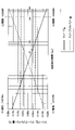
- It is a figure explaining the measuring method of the amount of creeps, and the amount of creep recovery.
- It is a figure which shows the film thickness of a resistor, the amount of creep, and the examination result of the amount of creep recovery.
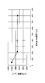
- FIG. 4 is a diagram showing experimental results of strain limits
- FIG. 3 is a cross-sectional view (part 3) illustrating the strain gauge according to the first embodiment
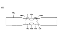
- FIG. 1 is a plan view illustrating a load cell according to a first embodiment
- FIG. 2 is a side view illustrating the load cell according to the first embodiment
- FIG. Referring to FIGS. 1 and 2, the load cell 100 has a strain body 110 and strain gauges 1 .
- the strain-generating body 110 is a Roberval-type strain-generating body in which a through hole 120, grooves 131, and grooves 132 are provided in a substantially rectangular parallelepiped metal block.
- the strain-generating body 110 is made of metal such as SUS304, an aluminum alloy, or iron, for example.
- the through hole 120 penetrates from one side surface of the strain generating body 110 to the other side surface.
- the through-hole 120 is formed, for example, in a spectacle-like shape in which, when viewed from the side, parts of opposing portions of two circular holes arranged apart from each other communicate with each other.
- the grooves 131 and 132 are arranged in the vertical direction of the strain body 110 so as to face each other with the through hole 120 interposed therebetween.
- the groove 131 is recessed from the upper surface of the strain body 110 toward the through hole 120 side
- the groove 132 is recessed from the lower surface of the strain body 110 toward the through hole 120 side.
- the portions sandwiched between the through-hole 120 and the grooves 131 and 132 are thin portions 141-144.
- the thin portions 141 to 144 are strain-generating portions in which strain is generated by an external force.
- Four strain gauges 1 are arranged in a matrix on the thin portion 141 and the thin portion 142 in the groove 131 .
- the grid direction of the resistor faces the longitudinal direction of the strain body 110, for example.
- Each strain gauge 1 is attached on the thin portion 141 and the thin portion 142 in the groove 131 via an adhesive layer, for example.
- the adhesive layer is not particularly limited as long as it is a material having a function of fixing the strain gauge 1 and the strain generating body 110, and can be appropriately selected according to the purpose. Examples include epoxy resin, modified epoxy resin, silicone resin, A modified silicone resin, a urethane resin, a modified urethane resin, or the like can be used. A material such as a bonding sheet may also be used.
- the thickness of the adhesive layer is not particularly limited and can be appropriately selected according to the purpose, and can be, for example, about 0.1 ⁇ m to 50 ⁇ m.
- the load cell 100 When the load cell 100 receives a load from the outside, stress is generated in the thin portions 141 to 144, which are strain-generating portions, and distortion occurs.
- the strain gauge 1 detects changes in resistance values caused by strains of the thin portions 141-144.
- the load received from the outside can be calculated by connecting four strain gauges 1 in a full bridge and arithmetically processing changes in resistance values.
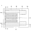
- FIG. 3 is a plan view illustrating the strain gauge according to the first embodiment
- FIG. FIG. 4 is a cross-sectional view (part 1) illustrating the strain gauge according to the first embodiment, showing a cross section along line AA in FIG.
- FIG. 5 is a cross-sectional view (No. 2) illustrating the strain gauge according to the first embodiment, showing a cross section along line BB in FIG.
- the strain gauge 1 has a base material 10, a resistor 30, a wiring 40, an electrode 50, and a cover layer 60. 3 to 5, for convenience, only the outer edge of the cover layer 60 is indicated by dashed lines. Note that the cover layer 60 may be provided as necessary.
- the side where the resistor 30 of the substrate 10 is provided is the upper side or one side, and the side where the resistor 30 is not provided is the lower side or the other side.
- the surface on the side where the resistor 30 of each part is provided is defined as one surface or upper surface, and the surface on the side where the resistor 30 is not provided is defined as the other surface or the lower surface.
- the strain gauge 1 can be used upside down or arranged at any angle.
- the term “planar view” refers to viewing an object from the direction normal to the upper surface 10a of the substrate 10
- the term “planar shape” refers to the shape of the object viewed from the direction normal to the upper surface 10a of the substrate 10.
- the base material 10 is a member that serves as a base layer for forming the resistor 30 and the like, and has flexibility.
- the film thickness of the base material 10 is not particularly limited and can be appropriately selected according to the purpose.
- the film thickness of the substrate 10 of 5 ⁇ m to 200 ⁇ m is preferable from the viewpoint of strain transmission and dimensional stability against the environment, and the film thickness of 10 ⁇ m or more is more preferable from the viewpoint of insulation.
- the substrate 10 is made of, for example, PI (polyimide) resin, epoxy resin, PEEK (polyetheretherketone) resin, PEN (polyethylene naphthalate) resin, PET (polyethylene terephthalate) resin, PPS (polyphenylene sulfide) resin, LCP (liquid crystal It can be formed from an insulating resin film such as polymer) resin, polyolefin resin, or the like. Note that the film refers to a flexible member having a film thickness of about 500 ⁇ m or less.
- the substrate 10 may be formed from, for example, an insulating resin film containing a filler such as silica or alumina.
- Materials other than the resin of the base material 10 include, for example, SiO 2 , ZrO 2 (including YSZ), Si, Si 2 N 3 , Al 2 O 3 (including sapphire), ZnO, perovskite ceramics (CaTiO 3 , BaTiO 3 ) and other crystalline materials, as well as amorphous glass and the like.
- a metal such as aluminum, an aluminum alloy (duralumin), or titanium may be used.
- an insulating film is formed on the base material 10 made of metal.
- the resistor 30 is a thin film formed in a predetermined pattern on the base material 10, and is a sensing part that undergoes a change in resistance when subjected to strain.
- the resistor 30 may be formed directly on the upper surface 10a of the base material 10, or may be formed on the upper surface 10a of the base material 10 via another layer.
- the resistor 30 is shown with a dark pear-skin pattern for the sake of convenience.
- the resistor 30 has a plurality of elongated portions arranged in the same longitudinal direction (the direction of line AA in FIG. 3) at predetermined intervals, and the ends of adjacent elongated portions are alternately connected. , is a zigzag folding structure as a whole.
- the longitudinal direction of the elongated portions is the grid direction, and the direction perpendicular to the grid direction is the grid width direction (the direction of line BB in FIG. 3).
- One ends in the longitudinal direction of the two elongated portions located on the outermost side in the grid width direction are bent in the grid width direction to form respective ends 30e1 and 30e2 of the resistor 30 in the grid width direction.
- Each end 30e1 and 30e2 of the resistor 30 in the grid width direction is electrically connected to the electrode 50 via the wiring 40.
- the wiring 40 electrically connects the ends 30e 1 and 30e 2 of the resistor 30 in the grid width direction and each electrode 50 .
- the resistor 30 can be made of, for example, a material containing Cr (chromium), a material containing Ni (nickel), or a material containing both Cr and Ni. That is, the resistor 30 can be made of a material containing at least one of Cr and Ni.
- Materials containing Cr include, for example, a Cr mixed phase film.
- Materials containing Ni include, for example, Cu—Ni (copper nickel).
- Materials containing both Cr and Ni include, for example, Ni—Cr (nickel chromium).
- the Cr mixed phase film is a film in which Cr, CrN, Cr 2 N, or the like is mixed.
- the Cr mixed phase film may contain unavoidable impurities such as chromium oxide.
- the stability of gauge characteristics can be improved by using ⁇ -Cr (alpha chromium), which is a stable crystal phase, as the main component.
- the gauge factor of the strain gauge 1 is 10 or more, and the temperature coefficient of gauge factor TCS and the temperature coefficient of resistance TCR are in the range of -1000 ppm/°C to +1000 ppm/°C.
- the term "main component" means that the target material accounts for 50% by weight or more of all the materials constituting the resistor. It preferably contains 90% by weight or more, more preferably 90% by weight or more.
- ⁇ -Cr is Cr with a bcc structure (body-centered cubic lattice structure).
- CrN and Cr 2 N contained in the Cr mixed phase film are preferably 20% by weight or less.
- CrN and Cr 2 N contained in the Cr mixed phase film are 20% by weight or less, a decrease in gauge factor can be suppressed.
- the ratio of Cr 2 N in CrN and Cr 2 N is preferably 80% by weight or more and less than 90% by weight, more preferably 90% by weight or more and less than 95% by weight.
- the ratio of Cr 2 N in CrN and Cr 2 N is 90% by weight or more and less than 95% by weight, the decrease in TCR (negative TCR) becomes more pronounced due to Cr 2 N having semiconducting properties. .
- by reducing ceramicization brittle fracture is reduced.
- the wiring 40 is formed on the base material 10 and electrically connected to the resistor 30 and the electrode 50 .
- the wiring 40 is not limited to a straight line, and may have any pattern. Also, the wiring 40 can be of any width and any length. In addition, in FIG. 3, the wiring 40 and the electrode 50 are shown with a pear-skin pattern that is thinner than the resistor 30 for the sake of convenience.
- the electrode 50 is formed on the base material 10 and electrically connected to the resistor 30 via the wiring 40.
- the electrode 50 is wider than the wiring 40 and formed in a substantially rectangular shape.
- the electrodes 50 are a pair of electrodes for outputting to the outside the change in the resistance value caused by the strain of the resistor 30, and are connected to, for example, lead wires for external connection.
- the resistor 30, the wiring 40, and the electrode 50 are given different symbols for convenience, they can be integrally formed from the same material in the same process. Therefore, the resistor 30, the wiring 40 and the electrode 50 have substantially the same thickness.
- a conductive layer made of a material having a resistance lower than that of the resistor 30 may be laminated on the wiring 40 and the electrode 50 .
- the material of the conductive layer to be laminated is not particularly limited as long as it has a lower resistance than that of the resistor 30, and can be appropriately selected according to the purpose.
- the resistor 30 is a Cr mixed phase film
- Cu, Ni, Al, Ag, Au, Pt, etc. alloys of any of these metals, compounds of any of these metals, or any of these Laminated films obtained by appropriately laminating metals, alloys, and compounds can be mentioned.
- the thickness of the conductive layer is not particularly limited and can be appropriately selected according to the purpose, and can be, for example, about 3 ⁇ m to 5 ⁇ m.
- the wiring 40 When a conductive layer made of a material having a lower resistance than that of the resistor 30 is laminated on the wiring 40 and the electrode 50 in this manner, the wiring 40 has a lower resistance than the resistor 30, and thus the wiring 40 is a resistor. It can be suppressed that it functions as As a result, the accuracy of strain detection by the resistor 30 can be improved.
- the wiring 40 having a resistance lower than that of the resistor 30 it is possible to limit the substantial sensing portion of the strain gauge 1 to the local area where the resistor 30 is formed. Therefore, the strain detection accuracy by the resistor 30 can be improved.
- the wiring 40 has a lower resistance than the resistor 30 and the resistor 30 is formed as a substantial sensing part. Restricting to a local region exhibits a significant effect in improving strain detection accuracy. Further, making the wiring 40 lower in resistance than the resistor 30 also has the effect of reducing lateral sensitivity.
- the cover layer 60 is formed on the base material 10 to cover the resistors 30 and the wirings 40 and expose the electrodes 50 . A portion of the wiring 40 may be exposed from the cover layer 60 .
- the cover layer 60 that covers the resistor 30 and the wiring 40, mechanical damage or the like to the resistor 30 and the wiring 40 can be prevented.
- the cover layer 60 the resistor 30 and the wiring 40 can be protected from moisture and the like. Note that the cover layer 60 may be provided so as to cover the entire portion excluding the electrode 50 .
- the cover layer 60 can be made of insulating resin such as PI resin, epoxy resin, PEEK resin, PEN resin, PET resin, PPS resin, composite resin (eg, silicone resin, polyolefin resin).
- the cover layer 60 may contain fillers or pigments.
- the thickness of the cover layer 60 is not particularly limited, and can be appropriately selected according to the purpose.
- resistor film thickness (1) a suitable film thickness of the resistor 30 when the strain gauge 1 is used for a weighing application will be described.
- Standards related to creep include, for example, accuracy grade C1 based on OIML R60 (hereinafter referred to as C1 standard) and accuracy grade C2 based on OIML R60 (hereinafter referred to as C2 standard).
- the C1 standard requires that the creep amount and creep recovery amount be ⁇ 0.0735% or less.
- the C2 standard requires that the amount of creep and the amount of creep recovery be ⁇ 0.0368% or less.
- the strain gauge 1 is used as a sensor, the standard for creep amount and creep recovery amount is about ⁇ 0.5%.
- a plurality of samples were prepared by changing the film thickness of the resistor 30 of the strain gauge 1 (in the four strain gauges 1, each The film thickness of the resistor 30 is the same), and the creep amount and creep recovery amount of each sample were measured.
- a polyimide resin film having a film thickness of 25 ⁇ m was used as the substrate 10 .
- a Cr mixed phase film was used for the resistor 30 .
- the FSU-15K is a load cell having a rated capacity of 15 kgf and having a Roberval type strain body made of SUS304.
- the amount of creep and the amount of creep recovery are the amounts of change over time in the amount of elastic deformation (strain amount) of the surface of the strain gauge 1 on which the resistor 30 is provided. can be measured by arithmetic processing. A detailed description will be given with reference to FIG.
- FIG. 6 is a diagram explaining a method for measuring the amount of creep and the amount of creep recovery.
- the horizontal axis is time
- the vertical axis is strain voltage [mV].
- the strain voltage changes, for example, as shown in FIG. In FIG. 6, the absolute value B of the strain voltage difference is measured 20 minutes after the 150% load is removed and immediately after the 100% load is applied.
- the absolute value ⁇ A of the difference in strain voltage immediately after application of 100% load and 20 minutes after the start of application of 100% load is measured. At this time, ⁇ A/B is the amount of creep.
- the absolute value ⁇ C of the difference in strain voltage immediately after the 100% load is removed and 20 minutes after the 100% load is removed is measured. At this time, ⁇ C/B is the amount of creep recovery.
- the 100% load is 2 kg, and the 150% load is 1.5 times the 100% load.
- FIG. 7 is a diagram showing the results of examination of the film thickness of the resistor, the amount of creep, and the amount of creep recovery. It summarizes the results measured by the measurement method.
- the C1 standard creep amount and creep recovery amount can be satisfied. Further, as shown in FIG. 7, when the film thickness of the resistor 30 is 11 nm or more and 50 nm or less, the C2 standard creep amount and creep recovery amount can be satisfied. That is, in the strain gauge 1 mounted on the Roberval type strain body, by controlling the film thickness of the resistor 30 within a predetermined range, the amount of creep and the amount of creep recovery are improved.
- the inventors have confirmed that the above film thickness range of the resistor 30 that satisfies the C1 standard or the C2 standard is established when at least the width of the resistor 30 is in the range of 50 ⁇ m or more and 500 ⁇ m or less.
- the film thickness of the resistor 30 that satisfies the creep amount and creep recovery amount of the C1 standard or C2 standard also depends on the structure of the strain-generating body. That is, the preferable film thickness range of the resistor 30 in the case of using the Roberval-type strain-generating body is as described above. The preferred film thickness range for 30 may differ from the above.
- strain limit is preferably improved as much as possible.
- the strain limit is the value of mechanical strain at which cracks or disconnections begin to occur when strain is applied to the strain gauge.
- the film thickness of the resistor 30 affects not only the creep but also the strain limit. In other words, it has been found that the thinner the film thickness of the resistor 30, the less likely cracks and disconnections will occur when the resistor 30 is strained.
- the inventors studied the film thickness of the resistor 30, which is necessary for improving the strain limit. Specifically, the inventors fabricated a plurality of strain gauges 1 of three types each having a thickness of 50 nm, 220 nm, and 800 nm for the resistor 30, applied strain to each strain, and investigated the occurrence of cracks and disconnections. rice field. In the strain gauge 1, a polyimide resin film having a film thickness of 25 ⁇ m was used as the substrate 10 . A Cr mixed phase film was used for the resistor 30 .
- Fig. 8 is a diagram showing the strain limit experimental results, plotting the minimum strain limit values of a plurality of strain gauges. As shown in FIG. 8, in the experimental results of the inventors, the strain limit was substantially constant at 7000 ⁇ or more when the film thickness of the resistor 30 was 220 nm and 800 nm, whereas the film thickness of the resistor 30 was The strain limit in the case of 50 nm was 10000 ⁇ or more.
- the film thickness of the resistor 30 is 11 nm or more and 50 nm or less, the C2 standard creep amount and creep recovery amount can be satisfied. In this case, regardless of the film thickness of the resistor 30, it can be said that there is a sufficient strain limit of 10000 ⁇ or more.
- the base material 10 is prepared, and a metal layer (referred to as metal layer A for convenience) is formed on the upper surface 10 a of the base material 10 .
- the metal layer A is a layer that is finally patterned to become the resistor 30 , the wiring 40 and the electrode 50 . Therefore, the material and thickness of the metal layer A are the same as those of the resistor 30, the wiring 40, and the electrode 50 described above.
- the metal layer A can be formed, for example, by magnetron sputtering using a raw material capable of forming the metal layer A as a target.
- the metal layer A may be formed by using a reactive sputtering method, a vapor deposition method, an arc ion plating method, a pulse laser deposition method, or the like instead of the magnetron sputtering method.
- a functional layer having a predetermined thickness is vacuum-formed on the upper surface 10a of the substrate 10 as a base layer by conventional sputtering, for example. is preferred.
- a functional layer refers to a layer having a function of promoting crystal growth of at least the upper metal layer A (resistor 30).
- the functional layer preferably further has a function of preventing oxidation of the metal layer A due to oxygen and moisture contained in the base material 10 and a function of improving adhesion between the base material 10 and the metal layer A.
- the functional layer may also have other functions.
- the insulating resin film that constitutes the base material 10 contains oxygen and moisture, especially when the metal layer A contains Cr, Cr forms a self-oxidizing film. Being prepared helps.
- the material of the functional layer is not particularly limited as long as it has a function of promoting the crystal growth of at least the upper metal layer A (resistor 30), and can be appropriately selected according to the purpose. Chromium), Ti (titanium), V (vanadium), Nb (niobium), Ta (tantalum), Ni (nickel), Y (yttrium), Zr (zirconium), Hf (hafnium), Si (silicon), C ( carbon), Zn (zinc), Cu (copper), Bi (bismuth), Fe (iron), Mo (molybdenum), W (tungsten), Ru (ruthenium), Rh (rhodium), Re (rhenium), Os ( osmium), Ir (iridium), Pt (platinum), Pd (palladium), Ag (silver), Au (gold), Co (cobalt), Mn (manganese), Al (aluminum) 1 selected from the group consisting of Metal or metals, alloys of any of this group of
- Examples of the above alloy include FeCr, TiAl, FeNi, NiCr, CrCu, and the like.
- Examples of the above compounds include TiN, TaN , Si3N4 , TiO2 , Ta2O5 , SiO2 and the like.
- the thickness of the functional layer is preferably 1/20 or less of the thickness of the resistor. Within this range, it is possible to promote the crystal growth of ⁇ -Cr, and to prevent a part of the current flowing through the resistor from flowing through the functional layer, thereby preventing a decrease in strain detection sensitivity.
- the thickness of the functional layer is more preferably 1/50 or less of the thickness of the resistor. Within this range, it is possible to promote the crystal growth of ⁇ -Cr, and further prevent the deterioration of the strain detection sensitivity due to part of the current flowing through the resistor flowing through the functional layer.
- the thickness of the functional layer is more preferably 1/100 or less of the thickness of the resistor. Within such a range, it is possible to further prevent a decrease in strain detection sensitivity due to part of the current flowing through the resistor flowing through the functional layer.
- the film thickness of the functional layer is preferably 1 nm to 1 ⁇ m. Within such a range, the crystal growth of ⁇ -Cr can be promoted, and the film can be easily formed without causing cracks in the functional layer.
- the thickness of the functional layer is more preferably 1 nm to 0.8 ⁇ m. Within such a range, the crystal growth of ⁇ -Cr can be promoted, and the functional layer can be formed more easily without cracks.
- the thickness of the functional layer is more preferably 1 nm to 0.5 ⁇ m. Within such a range, the crystal growth of ⁇ -Cr can be promoted, and the functional layer can be formed more easily without cracks.
- planar shape of the functional layer is patterned to be substantially the same as the planar shape of the resistor shown in FIG. 3, for example.
- the planar shape of the functional layer is not limited to being substantially the same as the planar shape of the resistor. If the functional layer is made of an insulating material, it may not be patterned in the same planar shape as the resistor. In this case, the functional layer may be solidly formed at least in the region where the resistor is formed. Alternatively, the functional layer may be formed all over the top surface of the substrate 10 .
- the thickness and surface area of the functional layer can be increased by forming the functional layer relatively thick such that the thickness is 50 nm or more and 1 ⁇ m or less and forming the functional layer in a solid manner. Since the resistance increases, the heat generated by the resistor can be dissipated to the base material 10 side. As a result, in the strain gauge 1, deterioration in measurement accuracy due to self-heating of the resistor can be suppressed.
- the functional layer can be formed, for example, by conventional sputtering using a raw material capable of forming the functional layer as a target and introducing Ar (argon) gas into the chamber in a vacuum.
- Ar argon
- the functional layer is formed while etching the upper surface 10a of the base material 10 with Ar. Therefore, the amount of film formation of the functional layer can be minimized and an effect of improving adhesion can be obtained.
- the functional layer may be formed by other methods.
- the upper surface 10a of the substrate 10 is activated by a plasma treatment using Ar or the like to obtain an effect of improving adhesion, and then the functional layer is vacuum-formed by magnetron sputtering. You may use the method to do.
- the combination of the material of the functional layer and the material of the metal layer A is not particularly limited and can be appropriately selected according to the purpose. It is possible to form a Cr mixed phase film as a main component.
- the metal layer A can be formed by magnetron sputtering using a raw material capable of forming a Cr mixed-phase film as a target and introducing Ar gas into the chamber.
- the metal layer A may be formed by reactive sputtering using pure Cr as a target, introducing an appropriate amount of nitrogen gas into the chamber together with Ar gas.
- the introduction amount and pressure (nitrogen partial pressure) of nitrogen gas and adjusting the heating temperature by providing a heating process by changing the introduction amount and pressure (nitrogen partial pressure) of nitrogen gas and adjusting the heating temperature by providing a heating process, the ratio of CrN and Cr 2 N contained in the Cr mixed phase film, and the ratio of CrN and Cr The proportion of Cr2N in 2N can be adjusted.
- the growth surface of the Cr mixed phase film is defined by the functional layer made of Ti, and a Cr mixed phase film whose main component is ⁇ -Cr, which has a stable crystal structure, can be formed.
- the diffusion of Ti constituting the functional layer into the Cr mixed phase film improves the gauge characteristics.
- the gauge factor of the strain gauge 1 can be 10 or more, and the temperature coefficient of gauge factor TCS and the temperature coefficient of resistance TCR can be set within the range of -1000 ppm/°C to +1000 ppm/°C.
- the Cr mixed phase film may contain Ti or TiN (titanium nitride).
- the functional layer made of Ti has the function of promoting the crystal growth of the metal layer A and the function of preventing oxidation of the metal layer A due to oxygen and moisture contained in the base material 10. , and the function of improving the adhesion between the substrate 10 and the metal layer A.
- Ta, Si, Al, or Fe is used as the functional layer instead of Ti.
- the functional layer below the metal layer A in this manner, it is possible to promote the crystal growth of the metal layer A, and the metal layer A having a stable crystal phase can be produced. As a result, in the strain gauge 1, the stability of gauge characteristics can be improved. Further, by diffusing the material forming the functional layer into the metal layer A, the gauge characteristics of the strain gauge 1 can be improved.
- the metal layer A is patterned by photolithography to form the resistor 30, the wiring 40, and the electrode 50.
- the strain gauge 1 is completed by providing a cover layer 60 covering the resistor 30 and the wiring 40 and exposing the electrodes 50 on the upper surface 10a of the base material 10, if necessary.
- a cover layer 60 for example, a semi-cured thermosetting insulating resin film is laminated on the upper surface 10a of the base material 10 so as to cover the resistors 30 and the wiring 40 and expose the electrodes 50, and is cured by heating.
- the cover layer 60 is formed by coating the upper surface 10a of the base material 10 with a liquid or paste thermosetting insulating resin so as to cover the resistors 30 and the wirings 40 and expose the electrodes 50, and heat and harden the resin. may be made.
- the strain gauge 1 when a functional layer is provided on the upper surface 10a of the substrate 10 as a base layer for the resistor 30, the wiring 40, and the electrodes 50, the strain gauge 1 has a cross-sectional shape shown in FIG.
- a layer indicated by reference numeral 20 is a functional layer.
- the planar shape of the strain gauge 1 when the functional layer 20 is provided is, for example, similar to that shown in FIG. However, as described above, the functional layer 20 may be formed solidly on part or all of the upper surface 10a of the base material 10 in some cases.
- each resistor may be connected by wiring provided on the substrate so as to be convenient for bridge connection.
- each resistor may be half-bridge connected.
- the resistor mounted on the load cell 100 is not limited to either the upper surface or the lower surface of the load cell 100, and may be mounted on both the upper surface and the lower surface.
- two resistors may be mounted on the top surface of the load cell 100 and two resistors may be mounted on the bottom surface.
Landscapes
- Physics & Mathematics (AREA)
- General Physics & Mathematics (AREA)
- Measurement Of Length, Angles, Or The Like Using Electric Or Magnetic Means (AREA)
- Measurement Of Force In General (AREA)
Priority Applications (3)
| Application Number | Priority Date | Filing Date | Title |
|---|---|---|---|
| US18/567,970 US20240271920A1 (en) | 2021-06-09 | 2022-03-24 | Strain gauge and load cell |
| CN202280040786.2A CN117425807A (zh) | 2021-06-09 | 2022-03-24 | 应变计、测力传感器 |
| EP22818183.0A EP4354106A4 (en) | 2021-06-09 | 2022-03-24 | Strain gauge |
Applications Claiming Priority (2)
| Application Number | Priority Date | Filing Date | Title |
|---|---|---|---|
| JP2021-096391 | 2021-06-09 | ||
| JP2021096391A JP7568583B2 (ja) | 2021-06-09 | 2021-06-09 | ひずみゲージ、ロードセル |
Publications (1)
| Publication Number | Publication Date |
|---|---|
| WO2022259701A1 true WO2022259701A1 (ja) | 2022-12-15 |
Family
ID=84425195
Family Applications (1)
| Application Number | Title | Priority Date | Filing Date |
|---|---|---|---|
| PCT/JP2022/013897 Ceased WO2022259701A1 (ja) | 2021-06-09 | 2022-03-24 | ひずみゲージ、ロードセル |
Country Status (5)
| Country | Link |
|---|---|
| US (1) | US20240271920A1 (https=) |
| EP (1) | EP4354106A4 (https=) |
| JP (3) | JP7568583B2 (https=) |
| CN (1) | CN117425807A (https=) |
| WO (1) | WO2022259701A1 (https=) |
Citations (6)
| Publication number | Priority date | Publication date | Assignee | Title |
|---|---|---|---|---|
| JP2001221696A (ja) | 2000-02-10 | 2001-08-17 | Res Inst Electric Magnetic Alloys | 感温感歪複合センサ |
| JP2002241113A (ja) * | 2001-02-13 | 2002-08-28 | Japan New Metals Co Ltd | 窒化クロム粉の製造方法 |
| JP2002361516A (ja) * | 2001-06-06 | 2002-12-18 | Mitsubishi Materials Corp | 高速重切削加工で積層被覆層がすぐれた耐チッピング性を発揮する表面被覆炭化タングステン基超硬合金製エンドミル |
| JP2021056149A (ja) * | 2019-10-01 | 2021-04-08 | ミネベアミツミ株式会社 | ひずみゲージ、センサモジュール |
| JP2021096391A (ja) | 2019-12-18 | 2021-06-24 | アルパイン株式会社 | 映像表示装置 |
| WO2021145342A1 (ja) * | 2020-01-15 | 2021-07-22 | ミネベアミツミ株式会社 | ひずみゲージ |
Family Cites Families (4)
| Publication number | Priority date | Publication date | Assignee | Title |
|---|---|---|---|---|
| JP2630859B2 (ja) * | 1991-03-01 | 1997-07-16 | 株式会社 寺岡精工 | 歪ゲージ式ロードセル |
| JP2008064497A (ja) * | 2006-09-05 | 2008-03-21 | Ishida Co Ltd | ロードセルユニット、重量選別機、および電子秤 |
| US9897495B2 (en) * | 2012-11-12 | 2018-02-20 | A&D Company, Limited | Roberval-type load cell |
| JP2019066313A (ja) * | 2017-09-29 | 2019-04-25 | ミネベアミツミ株式会社 | ひずみゲージ |
-
2021
- 2021-06-09 JP JP2021096391A patent/JP7568583B2/ja active Active
-
2022
- 2022-03-24 EP EP22818183.0A patent/EP4354106A4/en active Pending
- 2022-03-24 WO PCT/JP2022/013897 patent/WO2022259701A1/ja not_active Ceased
- 2022-03-24 US US18/567,970 patent/US20240271920A1/en active Pending
- 2022-03-24 CN CN202280040786.2A patent/CN117425807A/zh active Pending
-
2024
- 2024-10-03 JP JP2024174361A patent/JP7747844B2/ja active Active
-
2025
- 2025-09-18 JP JP2025155229A patent/JP7849558B2/ja active Active
Patent Citations (6)
| Publication number | Priority date | Publication date | Assignee | Title |
|---|---|---|---|---|
| JP2001221696A (ja) | 2000-02-10 | 2001-08-17 | Res Inst Electric Magnetic Alloys | 感温感歪複合センサ |
| JP2002241113A (ja) * | 2001-02-13 | 2002-08-28 | Japan New Metals Co Ltd | 窒化クロム粉の製造方法 |
| JP2002361516A (ja) * | 2001-06-06 | 2002-12-18 | Mitsubishi Materials Corp | 高速重切削加工で積層被覆層がすぐれた耐チッピング性を発揮する表面被覆炭化タングステン基超硬合金製エンドミル |
| JP2021056149A (ja) * | 2019-10-01 | 2021-04-08 | ミネベアミツミ株式会社 | ひずみゲージ、センサモジュール |
| JP2021096391A (ja) | 2019-12-18 | 2021-06-24 | アルパイン株式会社 | 映像表示装置 |
| WO2021145342A1 (ja) * | 2020-01-15 | 2021-07-22 | ミネベアミツミ株式会社 | ひずみゲージ |
Non-Patent Citations (1)
| Title |
|---|
| See also references of EP4354106A4 |
Also Published As
| Publication number | Publication date |
|---|---|
| EP4354106A1 (en) | 2024-04-17 |
| JP2025176183A (ja) | 2025-12-03 |
| JP7568583B2 (ja) | 2024-10-16 |
| JP7849558B2 (ja) | 2026-04-21 |
| US20240271920A1 (en) | 2024-08-15 |
| EP4354106A4 (en) | 2024-09-04 |
| JP2024174208A (ja) | 2024-12-13 |
| JP2022188394A (ja) | 2022-12-21 |
| JP7747844B2 (ja) | 2025-10-01 |
| CN117425807A (zh) | 2024-01-19 |
Similar Documents
| Publication | Publication Date | Title |
|---|---|---|
| JP7570975B2 (ja) | ひずみゲージ | |
| US11448560B2 (en) | Strain gauge and sensor module | |
| US12306053B2 (en) | Strain gauge including a barrier layer over a resistance body | |
| JP2024174184A (ja) | ひずみゲージ | |
| WO2021205981A1 (ja) | ひずみゲージ | |
| JP2023138686A (ja) | センサモジュール | |
| JP7755708B2 (ja) | ひずみゲージ | |
| JP2025142294A (ja) | ひずみゲージ | |
| WO2022259703A1 (ja) | ひずみゲージ | |
| WO2024029538A1 (ja) | ひずみゲージ | |
| WO2022259701A1 (ja) | ひずみゲージ、ロードセル | |
| JP7782115B2 (ja) | ひずみゲージ | |
| JP2022008026A (ja) | ひずみゲージ | |
| US12595998B2 (en) | Strain gauge | |
| US20250198737A1 (en) | Strain gauge | |
| WO2023139807A1 (ja) | ひずみゲージ | |
| WO2024029454A1 (ja) | ひずみゲージ | |
| WO2024010027A1 (ja) | ひずみゲージ | |
| JP2023136681A (ja) | ひずみゲージ | |
| JP2023037918A (ja) | ひずみゲージ |
Legal Events
| Date | Code | Title | Description |
|---|---|---|---|
| 121 | Ep: the epo has been informed by wipo that ep was designated in this application |
Ref document number: 22818183 Country of ref document: EP Kind code of ref document: A1 |
|
| WWE | Wipo information: entry into national phase |
Ref document number: 202280040786.2 Country of ref document: CN Ref document number: 18567970 Country of ref document: US |
|
| WWE | Wipo information: entry into national phase |
Ref document number: 2022818183 Country of ref document: EP |
|
| NENP | Non-entry into the national phase |
Ref country code: DE |
|
| ENP | Entry into the national phase |
Ref document number: 2022818183 Country of ref document: EP Effective date: 20240109 |