WO2022255388A1 - 高周波回路および通信装置 - Google Patents
高周波回路および通信装置 Download PDFInfo
- Publication number
- WO2022255388A1 WO2022255388A1 PCT/JP2022/022226 JP2022022226W WO2022255388A1 WO 2022255388 A1 WO2022255388 A1 WO 2022255388A1 JP 2022022226 W JP2022022226 W JP 2022022226W WO 2022255388 A1 WO2022255388 A1 WO 2022255388A1
- Authority
- WO
- WIPO (PCT)
- Prior art keywords
- line
- circuit
- amplifier
- sub
- main line
- Prior art date
- Legal status (The legal status is an assumption and is not a legal conclusion. Google has not performed a legal analysis and makes no representation as to the accuracy of the status listed.)
- Ceased
Links
Images




Classifications
-
- H—ELECTRICITY
- H03—ELECTRONIC CIRCUITRY
- H03F—AMPLIFIERS
- H03F1/00—Details of amplifiers with only discharge tubes, only semiconductor devices or only unspecified devices as amplifying elements
- H03F1/56—Modifications of input or output impedances, not otherwise provided for
- H03F1/565—Modifications of input or output impedances, not otherwise provided for using inductive elements
-
- H—ELECTRICITY
- H03—ELECTRONIC CIRCUITRY
- H03F—AMPLIFIERS
- H03F3/00—Amplifiers with only discharge tubes or only semiconductor devices as amplifying elements
- H03F3/20—Power amplifiers, e.g. Class B amplifiers, Class C amplifiers
- H03F3/21—Power amplifiers, e.g. Class B amplifiers, Class C amplifiers with semiconductor devices only
- H03F3/211—Power amplifiers, e.g. Class B amplifiers, Class C amplifiers with semiconductor devices only using a combination of several amplifiers
-
- H—ELECTRICITY
- H03—ELECTRONIC CIRCUITRY
- H03F—AMPLIFIERS
- H03F1/00—Details of amplifiers with only discharge tubes, only semiconductor devices or only unspecified devices as amplifying elements
- H03F1/02—Modifications of amplifiers to raise the efficiency, e.g. gliding Class A stages, use of an auxiliary oscillation
- H03F1/0205—Modifications of amplifiers to raise the efficiency, e.g. gliding Class A stages, use of an auxiliary oscillation in transistor amplifiers
- H03F1/0288—Modifications of amplifiers to raise the efficiency, e.g. gliding Class A stages, use of an auxiliary oscillation in transistor amplifiers using a main and one or several auxiliary peaking amplifiers whereby the load is connected to the main amplifier using an impedance inverter, e.g. Doherty amplifiers
-
- H—ELECTRICITY
- H03—ELECTRONIC CIRCUITRY
- H03F—AMPLIFIERS
- H03F3/00—Amplifiers with only discharge tubes or only semiconductor devices as amplifying elements
- H03F3/189—High-frequency amplifiers, e.g. radio frequency amplifiers
- H03F3/19—High-frequency amplifiers, e.g. radio frequency amplifiers with semiconductor devices only
- H03F3/195—High-frequency amplifiers, e.g. radio frequency amplifiers with semiconductor devices only in integrated circuits
-
- H—ELECTRICITY
- H03—ELECTRONIC CIRCUITRY
- H03F—AMPLIFIERS
- H03F3/00—Amplifiers with only discharge tubes or only semiconductor devices as amplifying elements
- H03F3/20—Power amplifiers, e.g. Class B amplifiers, Class C amplifiers
- H03F3/21—Power amplifiers, e.g. Class B amplifiers, Class C amplifiers with semiconductor devices only
- H03F3/213—Power amplifiers, e.g. Class B amplifiers, Class C amplifiers with semiconductor devices only in integrated circuits
-
- H—ELECTRICITY
- H03—ELECTRONIC CIRCUITRY
- H03F—AMPLIFIERS
- H03F3/00—Amplifiers with only discharge tubes or only semiconductor devices as amplifying elements
- H03F3/20—Power amplifiers, e.g. Class B amplifiers, Class C amplifiers
- H03F3/24—Power amplifiers, e.g. Class B amplifiers, Class C amplifiers of transmitter output stages
- H03F3/245—Power amplifiers, e.g. Class B amplifiers, Class C amplifiers of transmitter output stages with semiconductor devices only
-
- H—ELECTRICITY
- H03—ELECTRONIC CIRCUITRY
- H03F—AMPLIFIERS
- H03F3/00—Amplifiers with only discharge tubes or only semiconductor devices as amplifying elements
- H03F3/72—Gated amplifiers, i.e. amplifiers which are rendered operative or inoperative by means of a control signal
-
- H—ELECTRICITY
- H04—ELECTRIC COMMUNICATION TECHNIQUE
- H04B—TRANSMISSION
- H04B1/00—Details of transmission systems, not covered by a single one of groups H04B3/00 - H04B13/00; Details of transmission systems not characterised by the medium used for transmission
- H04B1/38—Transceivers, i.e. devices in which transmitter and receiver form a structural unit and in which at least one part is used for functions of transmitting and receiving
- H04B1/40—Circuits
-
- H—ELECTRICITY
- H03—ELECTRONIC CIRCUITRY
- H03F—AMPLIFIERS
- H03F2200/00—Indexing scheme relating to amplifiers
- H03F2200/111—Indexing scheme relating to amplifiers the amplifier being a dual or triple band amplifier, e.g. 900 and 1800 MHz, e.g. switched or not switched, simultaneously or not
-
- H—ELECTRICITY
- H03—ELECTRONIC CIRCUITRY
- H03F—AMPLIFIERS
- H03F2200/00—Indexing scheme relating to amplifiers
- H03F2200/451—Indexing scheme relating to amplifiers the amplifier being a radio frequency amplifier
-
- H—ELECTRICITY
- H03—ELECTRONIC CIRCUITRY
- H03F—AMPLIFIERS
- H03F2200/00—Indexing scheme relating to amplifiers
- H03F2200/537—A transformer being used as coupling element between two amplifying stages
-
- H—ELECTRICITY
- H03—ELECTRONIC CIRCUITRY
- H03F—AMPLIFIERS
- H03F2203/00—Indexing scheme relating to amplifiers with only discharge tubes or only semiconductor devices as amplifying elements covered by H03F3/00
- H03F2203/72—Indexing scheme relating to gated amplifiers, i.e. amplifiers which are rendered operative or inoperative by means of a control signal
- H03F2203/7209—Indexing scheme relating to gated amplifiers, i.e. amplifiers which are rendered operative or inoperative by means of a control signal the gated amplifier being switched from a first band to a second band
Definitions
- the present invention relates to high frequency circuits and communication devices.
- a first amplifier and a second amplifier are connected between the output terminal of the first amplifier and the output terminal of the second amplifier to adjust the phase of the output signal of the first amplifier.
- a power amplifier circuit includes an amplifier output phase shifter for outputting power, and a transformer connected to the output terminals of the amplifier output phase shifter and the second amplifier.
- the amplifier output phase shifter is a circuit for adjusting the phase for 1/4 wavelength. When configured, the power amplifier circuit becomes large.
- the present invention has been made to solve the above problems, and an object of the present invention is to provide a compact high-frequency circuit and communication device having a plurality of amplifying elements and phase shift circuits.
- a high-frequency circuit includes a first amplifying element and a second amplifying element, a transformer having an input side coil and an output side coil, a signal output terminal, a first circuit and, one end of the input side coil is connected to the output terminal of the first amplifying element, one end of the output side coil is connected to the signal output terminal, and the other end of the output side coil is connected to the ground
- the first circuit has a first main line and a first sub line, one end of the first main line is connected to the output terminal of the second amplifying element, and the first The other end of the main line is connected to the other end of the input side coil, one end of the first sub line is connected to one end of the first main line, and the other end of the first sub line is grounded.
- the first direction from one end to the other end of the first main line is the same as the second direction from the other end to the one end of the first sub-line.
- a high-frequency circuit includes a first amplifying element and a second amplifying element, a first transmission line, a signal output terminal, and a first circuit, wherein the first transmission line
- the first circuit is connected between the output terminal of the first amplifying element and the output terminal of the second amplifying element, the first circuit has a first main line and a first sub line, and one end of the first main line is connected to one end of the first transmission line, the other end of the first main line is connected to the signal output terminal, and the other end of the first transmission line is connected to the output terminal of the first amplifying element.
- one end of the first sub-line is connected to one end of the first main line, the other end of the first sub-line is connected to the ground, and from one end to the other end of the first main line
- the first direction is the same as the second direction from the other end to the one end of the first sub-line.
- FIG. 1 is a circuit configuration diagram of a high-frequency circuit and a communication device according to Embodiment 1.
- FIG. 2A is a circuit state diagram when a large signal is input to the amplifier circuit according to the first embodiment.
- FIG. 2B is a circuit state diagram when a small signal is input to the amplifier circuit according to the first embodiment.
- FIG. 3A is a circuit state diagram of a conventional Doherty amplifier circuit when a large signal is input.
- FIG. 3B is a circuit state diagram of a conventional Doherty amplifier circuit when a small signal is input.
- FIG. 4 is a graph comparing the amplification characteristics of the conventional amplifier circuit and the amplifier circuit according to the first embodiment.
- FIG. 1 is a circuit configuration diagram of a high-frequency circuit and a communication device according to Embodiment 1.
- FIG. 2A is a circuit state diagram when a large signal is input to the amplifier circuit according to the first embodiment.
- FIG. 2B is a circuit state diagram when a small signal is
- FIG. 5 is a circuit configuration diagram of a high frequency circuit and a communication device according to the second embodiment.
- 6A is a circuit state diagram when a large signal is input to the amplifier circuit according to Modification 1 of Embodiment 2.
- FIG. 6B is a circuit state diagram when a small signal is input to the amplifier circuit according to Modification 1 of Embodiment 2.
- FIG. 7A is a circuit state diagram when a large signal is input to the amplifier circuit according to Modification 2 of Embodiment 2.
- FIG. FIG. 7B is a circuit state diagram when a medium signal is input to the amplifier circuit according to Modification 2 of Embodiment 2;
- 7C is a circuit state diagram when a small signal is input to the amplifier circuit according to Modification 2 of Embodiment 2.
- FIG. 8A and 8B are a plan view and a cross-sectional view of a high-frequency circuit according to a second embodiment.
- FIG. 1 is a schematic diagram that has been appropriately emphasized, omitted, or adjusted in proportion to show the present invention, and is not necessarily strictly illustrated, and the actual shape, positional relationship, and ratio are different. may differ.
- substantially the same configurations are denoted by the same reference numerals, and redundant description may be omitted or simplified.
- connection means not only direct connection with connection terminals and/or wiring conductors, but also electrical connection via other circuit elements. Also, “connected between A and B” and “connected between A and B” mean being connected to A and B on a path connecting A and B.
- planar view means viewing an object by orthographically projecting it onto the xy plane from the z-axis positive direction side.
- the component is placed on the main surface of the board means that the component is placed on the main surface in contact with the main surface of the board, and in addition, the component is placed on the main surface without contacting the main surface. It includes being arranged above and being arranged such that a part of the component is embedded in the substrate from the main surface side.
- C is arranged at the intersection of the first direction of A and the second direction of B” means a straight line extending from an arbitrary point in A in the first direction in plan view. and a straight line extending in the second direction from any point in B is included in C.
- terms that indicate the relationship between elements such as “parallel” and “perpendicular” and terms that indicate the shape of an element such as “rectangular” do not express only strict meanings, but substantially equivalent terms. It means that the range includes an error of, for example, several percent.
- the first direction and the second direction are the same does not necessarily mean that the angle formed by the direction vector of the first direction and the direction vector of the second direction is strictly 0 degrees. It is defined as including an angle formed by two directional vectors of -10 degrees or more and +10 degrees or less.
- signal path refers to a transmission line composed of a wire through which a high-frequency signal propagates, an electrode directly connected to the wire, and a terminal directly connected to the wire or the electrode.
- FIG. 1 is a circuit configuration diagram of a high frequency circuit 1 and a communication device 8 according to the first embodiment.
- the communication device 8 includes a high frequency circuit 1, an antenna 6, and an RF signal processing circuit (RFIC) 7.
- RFIC RF signal processing circuit
- the high frequency circuit 1 transmits high frequency signals between the antenna 6 and the RFIC 7 .
- a detailed circuit configuration of the high-frequency circuit 1 will be described later.
- the antenna 6 is connected to the antenna connection terminal 102 of the high frequency circuit 1, transmits a high frequency signal output from the high frequency circuit 1, and receives a high frequency signal from the outside and outputs it to the high frequency circuit 1.
- the RFIC 7 is an example of a signal processing circuit that processes high frequency signals. Specifically, the RFIC 7 performs signal processing such as down-conversion on the received signal input via the receiving path of the high-frequency circuit 1, and converts the received signal generated by the signal processing into a baseband signal processing circuit (BBIC, not shown). Further, the RFIC 7 performs signal processing such as up-conversion on the transmission signal input from the BBIC, and outputs the transmission signal generated by the signal processing to the transmission path of the high frequency circuit 1 .
- the RFIC 7 also has a control section that controls the switches and amplification elements of the high-frequency circuit 1 . A part or all of the functions of the RFIC 7 as a control unit may be implemented outside the RFIC 7 , for example, in the BBIC or the high frequency circuit 1 .
- the RFIC 7 also functions as a control unit that controls the power supply voltage Vcc and the bias voltage Vbias supplied to each amplifier of the high frequency circuit 1 . Specifically, RFIC 7 outputs a digital control signal to high frequency circuit 1 . Each amplifier of the high frequency circuit 1 is supplied with the power supply voltage Vcc and the bias voltage Vbias controlled by the digital control signal.
- the RFIC 7 also functions as a control unit that controls connections of the switches 81 and 84 of the high-frequency circuit 1 based on the communication band (frequency band) used.
- the antenna 6 is not an essential component in the communication device 8 according to the present embodiment.
- the high frequency circuit 1 includes an amplifier circuit 10, filters 82 and 83, switches 81 and 84, an input terminal 101, and an antenna connection terminal .
- the input terminal 101 is connected to the RFIC 7 and the antenna connection terminal 102 is connected to the antenna 6 .
- the amplifier circuit 10 is a circuit that amplifies the band A and band B transmission signals input from the input terminal 101 .
- the high-frequency circuit 1 may include a first amplifier circuit that amplifies band A high-frequency signals and a second amplifier circuit that amplifies band B high-frequency signals.
- each of band A and band B is for a communication system built using radio access technology (RAT: Radio Access Technology). 3rd Generation Partnership Project), IEEE (Institute of Electrical and Electronics Engineers), etc.).
- RAT Radio Access Technology
- 3rd Generation Partnership Project 3rd Generation Partnership Project
- IEEE Institute of Electrical and Electronics Engineers
- as a communication system for example, 4G (4th Generation)-LTE (Long Term Evolution) system, 5G (5th Generation)-NR (New Radio) system, WLAN (Wireless Local Area Network) system, etc. can be used, but is not limited to these.
- the filter 82 is connected between the switches 81 and 84 and passes the transmission signal in the band A transmission band among the transmission signals amplified by the amplifier circuit 10 .
- the filter 83 is connected between the switches 81 and 84 and passes the transmission signal in the band B transmission band among the transmission signals amplified by the amplifier circuit 10 .
- each of the filters 82 and 83 may constitute a duplexer together with a reception filter, or may be one filter for transmission in a time division duplex (TDD) system.
- TDD time division duplex
- a switch for switching between transmission and reception is arranged at least one of the front stage and the rear stage of the one filter.
- the switch 81 has a common terminal, a first selection terminal and a second selection terminal.
- a common terminal is connected to the signal output terminal 200 of the amplifier circuit 10 .
- a first selection terminal is connected to the filter 82 and a second selection terminal is connected to the filter 83 .
- the switch 81 switches the connection between the amplifier circuit 10 and the filter 82 and the connection between the amplifier circuit 10 and the filter 83 .
- the switch 84 is an example of an antenna switch, is connected to the antenna connection terminal 102, switches connection and disconnection between the antenna connection terminal 102 and the filter 82, and connects and disconnects the antenna connection terminal 102 and the filter 83. switch.
- the high-frequency circuit 1 may include a receiving circuit for transmitting the reception signal received from the antenna 6 to the RFIC 7 .
- the high frequency circuit 1 comprises a low noise amplifier and a reception filter.
- an impedance matching circuit may be arranged between the signal output terminal 200 and the antenna connection terminal 102 .
- the high-frequency circuit 1 can transmit or receive high-frequency signals of either band A or band B. Furthermore, the high-frequency circuit 1 can perform at least one of simultaneous transmission, simultaneous reception, and simultaneous transmission/reception of band A and band B high-frequency signals.
- the high-frequency circuit 1 only needs to have at least the amplifier circuit 10 in the circuit configuration shown in FIG.
- the amplifier circuit 10 includes a carrier amplifier 11, a peak amplifier 12, a preamplifier 15, a phase shift circuit 70, a transformer 20, an impedance conversion circuit 30, and a signal output terminal 200. .
- the preamplifier 15 amplifies the band A and/or band B high frequency signal input from the input terminal 101 .
- Phase shift circuit 70 distributes signal RF0 output from preamplifier 15, and outputs the distributed signals RF1 and RF2 to carrier amplifier 11 and peak amplifier 12 via terminals 110 and 120, respectively. Phase shift circuit 70 then adjusts the phases of signals RF1 and RF2. For example, phase shift circuit 70 shifts signal RF2 by -90 degrees (delays it by 90 degrees) relative to RF1.
- the configurations of the preamplifier 15 and the phase shift circuit 70 are not limited to the configurations described above.
- the preamplifier 15 may be arranged before each of the carrier amplifier 11 and the peak amplifier 12 .
- the phase shift circuit 70 may be arranged before each preamplifier, or before each of the carrier amplifier 11 and the peak amplifier 12 .
- the amplifier circuit 10 does not have to include the preamplifier 15 and the phase shift circuit 70 .
- Each of carrier amplifier 11 and peak amplifier 12 has an amplification transistor.
- the amplification transistor is, for example, a bipolar transistor such as a heterojunction bipolar transistor (HBT) or a field effect transistor such as a MOSFET (Metal-Oxide-Semiconductor Field Effect Transistor).
- HBT heterojunction bipolar transistor
- MOSFET Metal-Oxide-Semiconductor Field Effect Transistor
- Carrier amplifier 11 is an example of a first amplification element, and is a class A (or class AB) amplifier circuit capable of amplifying all power levels of signal RF1. A highly efficient amplification operation is possible.
- the first amplifying element according to the present invention may be a class A (or class AB) amplifying circuit, and is not limited to a carrier amplifier.
- efficiency means power added efficiency
- the peak amplifier 12 is an example of a second amplifying element, and is, for example, a class C amplifier circuit capable of amplifying in a region where the power level of the signal RF2 is high. Since a bias voltage lower than that applied to the amplification transistor of the carrier amplifier 11 is applied to the amplification transistor of the peak amplifier 12, the higher the power level of the signal RF2, the lower the output impedance. As a result, the peak amplifier 12 can perform amplification operation with low distortion in the high output region.
- the second amplifying element according to the present invention may be a class C amplifying circuit, and is not limited to a peak amplifier.
- the transformer 20 has an input side coil 201 and an output side coil 202 .
- One end of the input side coil 201 is connected to the output terminal of the carrier amplifier 11 and the other end of the input side coil 201 is connected to the other end 31 b of the main line 301 of the impedance conversion circuit 30 .
- One end of the output side coil 202 is connected to the signal output terminal 200, and the other end of the output side coil 202 is connected to the ground.
- the voltages of the signal output from the carrier amplifier 11 and the signal output from the peak amplifier 12 are added, and the combined output signal is output from the signal output terminal 200.
- the impedance conversion circuit 30 is an example of a first circuit, has a main line 301 and a sub line 302, shifts the phase at both ends of the impedance conversion circuit 30, and converts the impedance at a predetermined conversion ratio.
- the main line 301 is an example of a first main line, and is a transmission line having a length of 1/8 wavelength or 1/16 wavelength, for example.
- One end 31 a of the main line 301 is connected to the output terminal of the peak amplifier 12
- the other end 31 b of the main line 301 is connected to the other end of the input side coil 201 .
- the sub-line 302 is an example of a first sub-line, and is, for example, a transmission line having a length of 1/8 wavelength or 1/16 wavelength.
- One end 32b of the sub-line 302 is connected to one end 31a of the main line 301, and the other end 32a of the sub-line 302 is grounded.
- the first direction from one end 31a to the other end 31b of the main line 301 and the second direction from the other end 32a to the one end 32b of the sub-line 302 are the same.
- the main line 301 and the sub line 302 are electromagnetically coupled.
- the first direction and the second direction are preferably the same.
- FIG. 2A is a circuit state diagram when a large signal is input to the amplifier circuit 10 according to the first embodiment.
- FIG. 2B is a circuit state diagram of the amplifier circuit 10 according to the first embodiment when a small signal is input.
- the impedance Zp (hereinafter referred to as carrier
- the output impedance Zp of the amplifier 11) and the impedance Zn when looking at the load side from the output terminal of the peak amplifier 12 (hereinafter referred to as the output impedance Zn of the peak amplifier 12) are expressed as in Equation 1. It is assumed that the transformer 20 transforms at a ratio of 1:m. Let V1 be the voltage across the input side coil 201, V2 be the voltage across the output side coil 202, and i1 be the currents flowing through the main line 301 and the sub line 302, respectively. Let Vo be the output voltage of each amplifier.
- RL be the impedance of the load connected to the signal output terminal 200 .
- the impedance conversion circuit 30 causes the impedance Zn at its input end (the output terminal of the peak amplifier 12) to be 1/4 times the impedance Zs at its output end (the other end of the input side coil 201). Obviously,
- Equation 2 when the carrier amplifier 11 is in operation (ON) and the peak amplifier 12 is not in operation (OFF) (when a small signal is input), the output impedance Zp of the carrier amplifier 11 is given by Equation 2 is represented as At this time, the output impedance Zn of the peak amplifier 12 is in an open state.
- the output impedance Zp of the carrier amplifier 11 is doubled when a small signal is input as compared to when a large signal is input. That is, when a small signal is input, the peak amplifier 12 is turned off and the output impedance Zp of the carrier amplifier 11 is increased, so that the amplifier circuit 10 can operate with high efficiency.
- the carrier amplifier 11 and the peak amplifier 12 operate to output a large power signal, and the output impedance Zn of the peak amplifier 12 is low, so that signal distortion can be suppressed. It becomes possible.
- the impedance conversion circuit 30 has the function of converting the impedances (Zn and Zs) at both ends of the impedance conversion circuit 30, and also shifts the phase of the signal output from the peak amplifier 12 by -90 degrees (90 delay).
- the phase of the signal output from the carrier amplifier 11 and the phase of the signal output from the peak amplifier 12 are aligned so as to be opposite in phase.
- the signal output from the carrier amplifier 11 and the signal output from the peak amplifier 12 are voltage-synthesized in the transformer 20 .
- the main line 301 and the sub-line 302 have lengths shorter than 1/4 wavelength, for example, 1/8 wavelength or 1/16 wavelength.
- FIG. 3A is a circuit state diagram of a conventional Doherty amplifier circuit 500 when a large signal is input.
- FIG. 3B is a circuit state diagram of the conventional Doherty amplifier circuit 500 when a small signal is input.
- a conventional Doherty amplifier circuit 500 differs from the amplifier circuit 10 according to the first embodiment in that a quarter-wave transmission line 530 is arranged instead of the impedance conversion circuit 30 .
- the circuit configuration of the conventional amplifier circuit 500 will be described below, focusing on the configuration different from that of the amplifier circuit 10 according to the embodiment.
- the quarter-wave transmission line 530 is arranged between the output terminal of the peak amplifier 12 and the other end of the input side coil 201 .
- the output impedance Zp of the carrier amplifier 11 and the output impedance Zn of the peak amplifier 12 are obtained by the formula 3. Note that the current flowing through the input side coil 201 is assumed to be i1.
- Equation 4 the output impedance Zp of the carrier amplifier 11 is given by Equation 4 is represented as At this time, the output impedance Zn of the peak amplifier 12 is in an open state.
- the output impedance Zp of the carrier amplifier 11 is doubled when a small signal is input as compared to when a large signal is input. That is, when a small signal is input, the peak amplifier 12 is turned off and the output impedance Zp of the carrier amplifier 11 is increased, so that the amplifier circuit 500 can operate with high efficiency.
- the carrier amplifier 11 and the peak amplifier 12 operate to output a large power signal, and the output impedance Zn of the peak amplifier 12 is low, so that signal distortion can be suppressed. It becomes possible.
- the quarter-wave transmission line 530 shifts the phase of the signal output from the peak amplifier 12 by -90 degrees (delays it by 90 degrees).
- the phase of the signal output from the carrier amplifier 11 and the phase of the signal output from the peak amplifier 12 are aligned so as to be opposite in phase.
- the signal output from the carrier amplifier 11 and the signal output from the peak amplifier 12 are voltage-synthesized in the transformer 20 .
- FIG. 4 is a graph comparing the amplification characteristics of the conventional amplifier circuit 500 and the amplifier circuit 10 according to the first embodiment.
- the horizontal axis represents the power level of the signal output from the signal output terminal 200
- the vertical axis represents the efficiency (power added efficiency) of each amplifier circuit.
- the conventional amplifier circuit 500 compared to an amplifier circuit in which both the carrier amplifier 11 and the peak amplifier 12 operate in class AB, the high impedance operation of the carrier amplifier 11 in the low output region and the high impedance operation in the high output region. Efficiency is improved due to low signal distortion due to the low impedance operation of peak amplifier 12 .
- the impedance conversion circuit 30 allows the carrier amplifier 11 to operate at a higher impedance and the peak amplifier in the high output region. 12's low impedance operation improves efficiency in the high power operation and mid power regions.
- the impedance conversion circuit 30 configured by a line shorter than 1/4-wavelength is arranged. can be made smaller.
- the high-frequency circuit 1 includes the carrier amplifier 11 and the peak amplifier 12, the transformer 20 having the input side coil 201 and the output side coil 202, the signal output terminal 200, and the impedance conversion circuit 30. , one end of the input side coil 201 is connected to the output terminal of the carrier amplifier 11, one end of the output side coil 202 is connected to the signal output terminal 200, and the other end of the output side coil 202 is grounded.
- the impedance conversion circuit 30 has a main line 301 and a sub line 302, one end 31a of the main line 301 is connected to the output terminal of the peak amplifier 12, and the other end 31a of the main line 301 is connected to The end 31b is connected to the other end of the input side coil 201, the one end 32b of the sub line 302 is connected to the one end 31a of the main line 301, the other end 32a of the sub line 302 is grounded, The first direction from one end 31a to the other end 31b of the main line 301 and the second direction from the other end 32a to the one end 32b of the sub-line 302 are the same.
- the impedance conversion circuit 30 configured by a line shorter than 1/4 wavelength is arranged, so that the high frequency circuit 1 can be miniaturized. Also, since the output impedance of the peak amplifier 12 can be reduced, signal distortion can be reduced in the high output region.
- the communication device 8 includes an RFIC 7 that processes high frequency signals, and a high frequency circuit 1 that transmits high frequency signals between the RFIC 7 and the antenna 6 .
- the effect of the high frequency circuit 1 can be realized by the communication device 8.
- FIG. 5 is a circuit configuration diagram of the high frequency circuit 2 and the communication device 9 according to the second embodiment.
- the communication device 9 includes a high frequency circuit 2, an antenna 6, and an RFIC 7.
- a communication device 9 according to the present embodiment differs from the communication device 8 according to the first embodiment only in the configuration of the high-frequency circuit 2 .
- the configuration of the high-frequency circuit 2 of the communication device 9 according to the present embodiment, which is different from that of the communication device 8 according to the first embodiment, will be described below.
- the high frequency circuit 2 includes an amplifier circuit 50, filters 82 and 83, switches 81 and 84, an input terminal 101, and an antenna connection terminal .
- a high-frequency circuit 2 according to the present embodiment differs from the high-frequency circuit 1 according to the first embodiment only in the configuration of an amplifier circuit 50 . In the following, the high-frequency circuit 2 according to the present embodiment will be described with a focus on the configuration of the amplifier circuit 50. FIG.
- the amplifier circuit 50 is a circuit that amplifies the band A and band B transmission signals input from the input terminal 101 .
- the high-frequency circuit 2 can transmit or receive a high-frequency signal of either band A or band B.
- FIG. Furthermore, the high-frequency circuit 2 is also capable of performing at least one of simultaneous transmission, simultaneous reception, and simultaneous transmission and reception of the band A and band B high-frequency signals.
- the high-frequency circuit 2 according to the present invention only needs to have at least the amplifier circuit 50 in the circuit configuration shown in FIG.
- the amplifier circuit 50 includes a carrier amplifier 11, a peak amplifier 12, a preamplifier 15, a phase shift circuit 70, a quarter-wave transmission line 40, an impedance conversion circuit 30, and a signal output terminal. 200;
- the preamplifier 15 and the phase shift circuit 70 have the same configurations and functions as the preamplifier 15 and the phase shift circuit 70 included in the amplifier circuit 10 according to the first embodiment, so description thereof will be omitted here.
- Each of carrier amplifier 11 and peak amplifier 12 has an amplification transistor.
- the amplification transistor is, for example, a bipolar transistor such as HBT or a field effect transistor such as MOSFET.
- Carrier amplifier 11 is an example of a first amplification element, and is a class A (or class AB) amplifier circuit capable of amplifying all power levels of signal RF1. A highly efficient amplification operation is possible.
- the peak amplifier 12 is an example of a second amplifying element, and is, for example, a class C amplifier circuit capable of amplifying in a region where the power level of the signal RF2 is high. Since a bias voltage lower than that applied to the amplification transistor of the carrier amplifier 11 is applied to the amplification transistor of the peak amplifier 12, the higher the power level of the signal RF2, the lower the output impedance. As a result, the peak amplifier 12 can perform amplification operation with low distortion in the high output region.
- the quarter-wave transmission line 40 is an example of a first transmission line, and is connected between the output terminal of the carrier amplifier 11 and the output terminal of the peak amplifier 12 .
- the quarter-wave transmission line 40 shifts the phase of the signal output from the carrier amplifier 11 by -90 degrees (delays it by 90 degrees).
- the phase of the signal output from the carrier amplifier 11 and the phase of the signal output from the peak amplifier 12 are aligned. As a result, the signal output from the carrier amplifier 11 and the signal output from the peak amplifier 12 are current-combined.
- the impedance conversion circuit 30 is an example of a first circuit, has a main line 301 and a sub line 302, shifts the phase at both ends of the impedance conversion circuit 30, and converts the impedance at a predetermined conversion ratio.
- the main line 301 is an example of a first main line, and is a transmission line having a length of 1/8 wavelength or 1/16 wavelength, for example.
- One end 31 a of the main line 301 is connected to one end of the quarter-wave transmission line 40 , and the other end 31 b of the main line 301 is connected to the signal output terminal 200 .
- the other end of the quarter-wave transmission line 40 is connected to the output terminal of the carrier amplifier 11 .
- the sub-line 302 is an example of a first sub-line, and is, for example, a transmission line having a length of 1/8 wavelength or 1/16 wavelength.
- One end 32b of the sub-line 302 is connected to one end 31a of the main line 301, and the other end 32a of the sub-line 302 is grounded.
- the first direction from one end 31a to the other end 31b of the main line 301 and the second direction from the other end 32a to the one end 32b of the sub-line 302 are the same.
- the main line 301 and the sub line 302 are electromagnetically coupled.
- the first direction and the second direction are preferably the same.
- the output impedance of the carrier amplifier 11 is higher when a small signal is input than when a large signal is input. That is, when a small signal is input, the peak amplifier 12 is turned off and the output impedance of the carrier amplifier 11 is increased, so that the amplifier circuit 50 can operate with high efficiency.
- the carrier amplifier 11 and the peak amplifier 12 operate so that a large power signal can be output, and the output impedance of the peak amplifier 12 is lowered, thereby suppressing signal distortion. It becomes possible.
- the impedance conversion circuit 30 configured by a line shorter than 1/4-wavelength is arranged. Can be made smaller.
- the high-frequency circuit 2 according to the present embodiment may include the amplifier circuit 51 according to Modification 1 instead of the amplifier circuit 50 .
- the circuit configuration and operation of the amplifier circuit 51 according to Modification 1 will be described below.
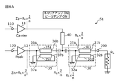
- FIG. 6A is a circuit state diagram when a large signal is input to the amplifier circuit 51 according to Modification 1 of Embodiment 2.
- FIG. 6B is a circuit state diagram when a small signal is input to the amplifier circuit 51 according to the first modification of the second embodiment.
- amplifier circuit 51 according to modification 1 includes carrier amplifier 11, peak amplifier 12, quarter-wave transmission line 40, impedance conversion circuits 30 and 35, and signal output terminal 200. And prepare.
- the amplifier circuit 51 may include the preamplifier 15 and the phase shift circuit 70 .
- An amplifier circuit 51 according to this modification differs from the amplifier circuit 50 according to the second embodiment only in that an impedance conversion circuit 35 is added.
- the description of the amplifier circuit 51 that is the same as that of the amplifier circuit 50 will be omitted, and the different points will be mainly described.
- the impedance conversion circuit 30 is an example of a first circuit, has a main line 301 and a sub line 302, shifts the phase at both ends of the impedance conversion circuit 30, and converts the impedance at a predetermined conversion ratio.
- the main line 301 is an example of a first main line, and is, for example, a transmission line having a length of 1/16 wavelength.
- One end 31 a of the main line 301 is connected to one end of the quarter-wave transmission line 40 , and the other end 31 b of the main line 301 is connected to the signal output terminal 200 .
- the other end of the quarter-wave transmission line 40 is connected to the output terminal of the carrier amplifier 11 .
- the sub-line 302 is an example of a first sub-line and is, for example, a transmission line having a length of 1/16 wavelength.
- One end 32b of the sub-line 302 is connected to one end 31a of the main line 301, and the other end 32a of the sub-line 302 is grounded.
- the first direction from one end 31a to the other end 31b of the main line 301 and the second direction from the other end 32a to the one end 32b of the sub-line 302 are the same.
- the main line 301 and the sub line 302 are electromagnetically coupled.
- the first direction and the second direction are preferably the same.
- the impedance conversion circuit 35 is an example of a second circuit, has a main line 351 and a sub line 352, shifts the phase at both ends of the impedance conversion circuit 35, and converts the impedance at a predetermined conversion ratio.
- the main line 351 is an example of a second main line, and is a transmission line having a length of 1/16 wavelength, for example.
- One end 36 a of the main line 351 is connected to the output terminal of the peak amplifier 12
- the other end 36 b of the main line 351 is connected to one end of the quarter-wave transmission line 40 and one end 31 a of the main line 301 .
- the sub-line 352 is an example of a second sub-line and is, for example, a transmission line having a length of 1/16 wavelength.
- One end 37b of the sub-line 352 is connected to one end 36a of the main line 351, and the other end 37a of the sub-line 352 is grounded.
- the third direction from the one end 36a to the other end 36b of the main line 351 and the fourth direction from the other end 37a to the one end 37b of the sub-line 352 are the same.
- the main line 351 and the sub line 352 are electromagnetically coupled.
- the third direction and the fourth direction are preferably the same.
- the output impedance Zp of the carrier amplifier 11 and the output impedance Zn of the peak amplifier 12 are obtained by the formula 5. It is assumed that the impedance conversion circuit 30 converts the impedance of the input end to 1/n of the impedance of the output end of the impedance conversion circuit 30 . Also, the impedance conversion circuit 35 converts the impedance of the input terminal to 1/n of the impedance of the output terminal of the impedance conversion circuit 35 . Let RL be the impedance of the load connected to the signal output terminal 200 . As shown in Equation 5, the impedance conversion circuits 30 and 35 make the output impedance Zn of the peak amplifier 12 1/n of the output impedance Zp of the carrier amplifier 11 .
- Equation 6 when the carrier amplifier 11 is in operation (ON) and the peak amplifier 12 is not in operation (OFF) (at the time of small signal input), the output impedance Zp of the carrier amplifier 11 is given by Equation 6 is represented as At this time, the output impedance Zn of the peak amplifier 12 is in an open state.
- the output impedance Zp of the carrier amplifier 11 is doubled when a small signal is input as compared to when a large signal is input. That is, when a small signal is input, the peak amplifier 12 is turned off and the output impedance Zp of the carrier amplifier 11 is increased, so that the amplifier circuit 51 can operate with high efficiency.
- the carrier amplifier 11 and the peak amplifier 12 operate so that a large power signal can be output.
- the output impedance Zn of the peak amplifier 12 is low, so that signal distortion can be suppressed.
- the impedance conversion circuits 30 and 35 configured by lines shorter than 1/4 wavelength are arranged instead of the 1/4 wavelength transmission line. can be made smaller.
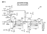
- FIG. 7A is a circuit state diagram when a large signal is input to amplifier circuit 52 according to Modification 2 of Embodiment 2.
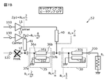
- FIG. 7B is a circuit state diagram of the amplifier circuit 52 according to Modification 2 of Embodiment 2 when a medium signal is input.
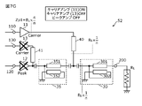
- FIG. 7C is a circuit state diagram when a small signal is input to the amplifier circuit 52 according to the second modification of the second embodiment.
- an amplifier circuit 52 according to Modification 2 includes carrier amplifiers 11 and 13, a peak amplifier 12, quarter-wave transmission lines 40 and 41, impedance conversion circuits 30 and 35, and a signal output terminal 200 .
- the amplifier circuit 52 may include the preamplifier 15 and the phase shift circuit 70 .
- Amplifier circuit 52 according to this modification differs from amplifier circuit 51 according to Modification 1 of Embodiment 2 only in that carrier amplifier 13 and quarter-wave transmission line 41 are added.
- the description of the amplifier circuit 52 that is the same as that of the amplifier circuit 51 will be omitted, and the different points will be mainly described.
- Carrier amplifier 13 is an example of a third amplifying element, and is a class A (or class AB) amplifier circuit capable of amplifying all power levels of the signal input from terminal 130, particularly in the middle output range. A highly efficient amplification operation is possible in
- the quarter-wave transmission line 41 is an example of a second transmission line, and one end of the quarter-wave transmission line 41 is connected to the output terminal of the carrier amplifier 13. The end is connected to the output terminal of the peak amplifier 12 and one end 36 a of the main line 351 .
- the quarter-wave transmission line 41 shifts the phase of the signal output from the carrier amplifier 13 by -90 degrees (delays it by 90 degrees). By disposing the quarter-wave transmission line 41, the phase of the signal output from the carrier amplifier 13 and the phase of the signal output from the peak amplifier 12 are aligned. As a result, the signal output from the carrier amplifier 13 and the signal output from the peak amplifier 12 are current-combined.
- Equation 7 when the carrier amplifiers 11 and 13 and the peak amplifier 12 are operating (ON) (when a large signal is input), the output impedance Zp1 of the carrier amplifier 11 and the output impedance Zp2 of the carrier amplifier 13 , and the output impedance Zn of the peak amplifier 12 are expressed as in Equation 7. As shown in Equation 7, the impedance conversion circuits 30 and 35 make the output impedance Zn of the peak amplifier 12 2/n of the output impedance Zp1 of the carrier amplifier 11 .
- the output impedance Zp1 of the carrier amplifier 11 and An output impedance Zp2 of the carrier amplifier 13 is expressed as in Equation (8).
- the output impedance Zn of the peak amplifier 12 is in an open state.
- the impedance conversion circuit 35 doubles the output impedance Zp2 of the carrier amplifier 13 as compared to the output impedance Zp2 of the carrier amplifier 13 when a large signal is input.
- the output impedance Zp1 of the carrier amplifier 11 is expressed as in Equation 9. At this time, the output impedances of the carrier amplifier 13 and the peak amplifier 12 are in an open state.
- the output impedance Zp1 of the carrier amplifier 11 is doubled when a small signal is input as compared to when a medium signal is input. That is, when a small signal is input, the carrier amplifier 13 and the peak amplifier 12 are turned off, and the output impedance Zp1 of the carrier amplifier 11 increases, so that the amplifier circuit 52 can operate with high efficiency.
- the carrier amplifiers 11 and 13 and the peak amplifier 12 operate to output a large power signal, and the output impedance Zn of the peak amplifier 12 is low, thereby suppressing signal distortion. It becomes possible to
- the output impedance Zp1 of the carrier amplifier 11 increases as the signal transitions from large signal input to medium signal input to small signal input.
- the amplifier circuit 52 according to the present modified example compared with the amplifier circuit 51 according to the first modified example, the outputs of the carrier amplifiers 11 and 13 according to the large signal output, the medium signal input, and the small signal input Since the impedance can be finely set, the efficiency can be improved with higher accuracy.
- FIG. 8 is a plan view and cross-sectional view of a high-frequency circuit 2 according to Embodiment 2.
- FIG. (a) of FIG. 8 shows a perspective view of the arrangement of circuit components when the main surface of the substrate 60 is viewed from the positive direction of the z-axis, and (b) of FIG. A cross-sectional view along line VIIIB-VIIIB of a) is shown.
- each circuit component may have a mark representing its function so that the layout relationship of each circuit component can be easily understood. , the mark is not affixed.
- illustration of the wiring that connects the substrate 60 and each circuit component is omitted.
- the high-frequency circuit 2 may further include a resin member covering the surface of the substrate 60 and part of the circuit components, and a shield electrode layer covering the surface of the resin member. Illustration of electrode layers is omitted.
- the high frequency circuit 2 further has a substrate 60 and a power supply line 90 in addition to the circuit configuration shown in FIG.
- the board 60 is a board on which circuit components that make up the high-frequency circuit 2 are mounted.
- the substrate 60 for example, a low temperature co-fired ceramics (LTCC) substrate having a laminated structure of a plurality of dielectric layers, a high temperature co-fired ceramics (HTCC) substrate, parts A built-in substrate, a substrate having a redistribution layer (RDL), a printed substrate, or the like is used.
- LTCC low temperature co-fired ceramics
- HTCC high temperature co-fired ceramics
- RDL redistribution layer
- a carrier amplifier 11, a peak amplifier 12, a capacitive element, and the like are arranged on the surface of the substrate 60.
- FIG. 1 A carrier amplifier 11, a peak amplifier 12, a capacitive element, and the like are arranged on the surface of the substrate 60.
- the carrier amplifiers 11 and 13 are included in a semiconductor IC.
- a semiconductor IC is arranged on the substrate 60 .
- a semiconductor IC is configured using, for example, CMOS (Complementary Metal Oxide Semiconductor), and may be specifically manufactured by an SOI (Silicon on Insulator) process.
- the semiconductor IC may be made of at least one of GaAs, SiGe and GaN. Note that the semiconductor material of the semiconductor IC is not limited to the materials described above. At least one of preamplifier 15, phase shift circuit 70, and switches 81 and 84 may be included in a semiconductor IC.
- a main line 301 and a sub line 302 (not shown) of the impedance conversion circuit 30 are formed on or inside the substrate 60 .
- the main line 301 and the sub-line 302 are composed of planar conductors formed on or inside the substrate 60 .
- the main line 301 and the sub-line 302 may be formed in the same layer of the substrate 60, or may be formed in different layers. Also, each of the main line 301 and the sub-line 302 may be formed over a plurality of layers.
- the power supply line 90 is a wiring that is connected to the carrier amplifier 11 and the peak amplifier 12 and supplies a power supply voltage to the carrier amplifier 11 and the peak amplifier 12 .
- the power line 90 is formed on or inside the substrate 60 .
- the power supply line 90 is composed of a planar conductor formed on the surface of or inside the substrate 60 .
- the main line 301 and the sub-line 302 are arranged on or inside the substrate 60 in the fifth direction (y-axis direction in FIG. 8) of the peak amplifier 12 .
- the power supply line 90 is on the surface or inside the substrate 60 and is perpendicular to the fifth direction of the carrier amplifier 11 (the y-axis direction in FIG. 8) and the fifth direction of the main line 301 and the sub line 302. It is arranged at the intersection with the sixth direction (the x-axis direction in FIG. 8).
- the distance between the main line 301 and the sub-line 302 and the peak amplifier 12 can be reduced, and the power supply line 90 can be arranged by effectively utilizing the space at the intersection. Therefore, the high frequency circuit 2 can be miniaturized while reducing the transmission loss of the high frequency circuit 2 .
- the high-frequency circuit 2 includes the carrier amplifier 11 and the peak amplifier 12, the quarter-wave transmission line 40, the signal output terminal 200, and the impedance conversion circuit 30.
- the /4 wavelength transmission line 40 is connected between the output terminal of the carrier amplifier 11 and the output terminal of the peak amplifier 12, the impedance conversion circuit 30 has a main line 301 and a sub line 302, One end 31a of the main line 301 is connected to one end of the quarter-wave transmission line 40, the other end 31b of the main line 301 is connected to the signal output terminal 200, and the other end of the quarter-wave transmission line 40 is connected to the signal output terminal 200.
- one end 32b of the sub line 302 is connected to one end 31a of the main line 301, the other end 32a of the sub line 302 is grounded, and the main line
- the first direction from one end 31a to the other end 31b of the sub-line 301 and the second direction from the other end 32a to the one end 32b of the sub-line 302 are the same.
- the impedance conversion circuit 30 configured by a line shorter than 1/4 wavelength is arranged, so that the high frequency circuit 2 can be miniaturized.
- the high-frequency circuit 2 further includes an impedance conversion circuit 35.
- the impedance conversion circuit 35 has a main line 351 and a sub-line 352.
- One end 36a of the main line 351 is the output terminal of the peak amplifier 12.
- the other end of the main line 351 is connected to one end of the quarter-wave transmission line 40 and one end 31a of the main line 301
- one end 37b of the sub-line 352 is connected to one end 36a of the main line 351.
- the other end of the sub-line 352 is connected to the ground, the third direction from the one end 36a of the main line 351 to the other end 36b, and the fourth direction from the other end 37a to the one end 37b of the sub-line 352. may be the same.
- the impedance conversion circuits 30 and 35 configured by lines shorter than 1/4 wavelength are arranged, so that the high frequency circuit 2 can be miniaturized. Also, since the output impedance of the peak amplifier 12 can be reduced, signal distortion can be reduced in the high output region.
- the high-frequency circuit 2 further includes a carrier amplifier 13 and a quarter-wave transmission line 41.
- One end of the quarter-wave transmission line 41 is connected to an output terminal of the carrier amplifier 13.
- the other end of the /4 wavelength transmission line 41 may be connected to the output terminal of the peak amplifier 12 and one end 36 a of the main line 351 .
- the output impedance of the carrier amplifier 13 can be increased in the low output range and the medium output range, thereby promoting high efficiency.
- the high-frequency circuit 2 further includes a substrate 60 and a power supply line 90 connected to the carrier amplifier 11 and the peak amplifier 12 for supplying a power supply voltage to the carrier amplifier 11 and the peak amplifier 12.
- 11 and the peak amplifier 12 are arranged on or inside the substrate 60, and when the substrate 60 is viewed from above, the main line 301 and the sub-line 302 extend on the surface or inside the substrate 60 in the fifth direction of the peak amplifier 12.
- the power supply line 90 is located on or inside the substrate 60 at the intersection of the fifth direction of the carrier amplifier 11 and the sixth direction orthogonal to the fifth direction of the main line 301 and the sub-line 302. may be placed.
- the distance between the main line 301 and the sub-line 302 and the peak amplifier 12 can be reduced, and the power supply line 90 can be arranged by effectively utilizing the space at the intersection. Therefore, the high frequency circuit 2 can be miniaturized while reducing the transmission loss of the high frequency circuit 2 .
- the carrier amplifier 11 and the peak amplifier 12 may be included in a semiconductor IC, and the semiconductor IC may be arranged on the substrate 60 .
- the high frequency circuit 2 can be miniaturized.
- the communication device 9 includes an RFIC 7 that processes high frequency signals, and a high frequency circuit 2 that transmits high frequency signals between the RFIC 7 and the antenna 6 .
- the effect of the high frequency circuit 2 can be realized by the communication device 9.
- the high-frequency circuits and communication devices according to the embodiments of the present invention have been described with reference to the embodiments and modifications, but the high-frequency circuits and communication devices according to the present invention are limited to the above-described embodiments and modifications. not to be Another embodiment realized by combining arbitrary components in the above embodiments and modifications, and various modifications that a person skilled in the art can think of without departing from the scope of the present invention with respect to the above embodiments and modifications
- the present invention also includes modified examples obtained by applying the above-described high-frequency circuit and communication device.
- the present invention can be widely used in communication equipment such as mobile phones as a high-frequency circuit arranged in the front-end part supporting multiband.
Landscapes
- Engineering & Computer Science (AREA)
- Power Engineering (AREA)
- Microelectronics & Electronic Packaging (AREA)
- Computer Networks & Wireless Communication (AREA)
- Signal Processing (AREA)
- Amplifiers (AREA)
Abstract
高周波回路(1)は、キャリアアンプ(11)およびピークアンプ(12)と、トランス(20)と、インピーダンス変換回路(30)と、を備え、入力側コイル(201)の一端はキャリアアンプ(11)の出力端子に接続され、出力側コイル(202)の一端は信号出力端子(200)に接続され、インピーダンス変換回路(30)は、主線路(301)と、副線路(302)と、を有し、主線路(301)の一端(31a)はピークアンプ(12)の出力端子に接続され、主線路(301)の他端(31b)は入力側コイル(201)の他端に接続され、副線路(302)の一端(32b)は主線路(301)の一端(31a)に接続され、副線路(302)の他端(32a)はグランドに接続され、主線路(301)の一端(31a)から他端(31b)へ向かう第1方向と、副線路(302)の他端(32a)から一端(32b)へ向かう第2方向とは、同じである。
Description
本発明は、高周波回路および通信装置に関する。
特許文献1には、第1のアンプおよび第2のアンプと、第1のアンプの出力端子と第2のアンプの出力端子との間に接続され、第1のアンプの出力信号の位相を調整するアンプ出力移相器と、アンプ出力移相器および第2のアンプの出力端子に接続されたトランスフォーマと、を備えた電力増幅回路が開示されている。
特許文献1に開示された電力増幅回路において、アンプ出力移相器は、1/4波長分の位相を調整するための回路であるため、インダクタおよびキャパシタで構成される場合、または、伝送線路で構成される場合に、電力増幅回路が大型化してしまう。
本発明は、上記課題を解決するためになされたものであって、複数の増幅素子および移相回路を有する、小型の高周波回路および通信装置を提供することを目的とする。
上記目的を達成するために、本発明の一態様に係る高周波回路は、第1増幅素子および第2増幅素子と、入力側コイルおよび出力側コイルを有するトランスと、信号出力端子と、第1回路と、を備え、入力側コイルの一端は、第1増幅素子の出力端子に接続されており、出力側コイルの一端は、信号出力端子に接続されており、出力側コイルの他端は、グランドに接続されており、第1回路は、第1主線路と、第1副線路と、を有し、第1主線路の一端は、第2増幅素子の出力端子に接続されており、第1主線路の他端は、入力側コイルの他端に接続されており、第1副線路の一端は、第1主線路の一端に接続されており、第1副線路の他端は、グランドに接続されており、第1主線路の一端から他端へ向かう第1方向と、第1副線路の他端から一端へ向かう第2方向とは、同じである。
また、本発明の一態様に係る高周波回路は、第1増幅素子および第2増幅素子と、第1伝送線路と、信号出力端子と、第1回路と、を備え、第1伝送線路は、第1増幅素子の出力端子と第2増幅素子の出力端子との間に接続されており、第1回路は、第1主線路と、第1副線路と、を有し、第1主線路の一端は、第1伝送線路の一端に接続されており、第1主線路の他端は、信号出力端子に接続されており、第1伝送線路の他端は、第1増幅素子の出力端子に接続されており、第1副線路の一端は、第1主線路の一端に接続されており、第1副線路の他端は、グランドに接続されており、第1主線路の一端から他端へ向かう第1方向と、第1副線路の他端から一端へ向かう第2方向とは、同じである。
本発明によれば、複数の増幅素子および移相回路を有する、高周波回路および通信装置を提供することが可能となる。
以下、本発明の実施の形態について、図面を用いて詳細に説明する。なお、以下で説明する実施の形態は、いずれも包括的または具体的な例を示すものである。以下の実施の形態で示される数値、形状、材料、構成要素、構成要素の配置および接続形態などは、一例であり、本発明を限定する主旨ではない。
なお、各図は、本発明を示すために適宜強調、省略、または比率の調整を行った模式図であり、必ずしも厳密に図示されたものではなく、実際の形状、位置関係、および比率とは異なる場合がある。各図において、実質的に同一の構成に対しては同一の符号を付しており、重複する説明は省略または簡素化される場合がある。
本開示において、「接続される」とは、接続端子および/または配線導体で直接接続される場合だけでなく、他の回路素子を介して電気的に接続される場合も含むことを意味する。また、「AとBとの間に接続される」、「AおよびBの間に接続される」とは、AおよびBを結ぶ経路上でAおよびBと接続されることを意味する。
また、本開示において、「平面視」とは、z軸正方向側からxy平面に物体を正投影して見ることを意味する。「部品が基板の主面に配置される」とは、部品が基板の主面と接触した状態で主面上に配置されることに加えて、部品が主面と接触せずに主面の上方に配置されること、および、部品の一部が主面側から基板内に埋め込まれて配置されることを含む。
また、本開示において、「CがAの第1方向とBの第2方向との交差部分に配置されている」とは、平面視において、A内の任意の点から第1方向に伸びる直線とB内の任意の点から第2方向に伸びる直線との交点がCに含まれることを意味する。また、「平行」および「垂直」などの要素間の関係性を示す用語、および、「矩形」などの要素の形状を示す用語は、厳格な意味のみを表すのではなく、実質的に同等な範囲、例えば数%程度の誤差をも含むことを意味する。また、「第1方向と第2方向とが同じである」とは、第1方向の方向ベクトルと第2方向の方向ベクトルとのなす角度が厳密に0度であることに限らず、当該2つの方向ベクトルのなす角度が-10度以上かつ+10度以下であることを含むものと定義される。
また、本開示において、「信号経路」とは、高周波信号が伝搬する配線、当該配線に直接接続された電極、および当該配線または当該電極に直接接続された端子等で構成された伝送線路であることを意味する。
(実施の形態1)
[1.高周波回路1および通信装置8の回路構成]
本実施の形態に係る高周波回路1および通信装置8の回路構成について、図1を参照しながら説明する。図1は、実施の形態1に係る高周波回路1および通信装置8の回路構成図である。
[1.高周波回路1および通信装置8の回路構成]
本実施の形態に係る高周波回路1および通信装置8の回路構成について、図1を参照しながら説明する。図1は、実施の形態1に係る高周波回路1および通信装置8の回路構成図である。
[1.1 通信装置8の回路構成]
まず、通信装置8の回路構成について説明する。図1に示すように、本実施の形態に係る通信装置8は、高周波回路1と、アンテナ6と、RF信号処理回路(RFIC)7と、を備える。
まず、通信装置8の回路構成について説明する。図1に示すように、本実施の形態に係る通信装置8は、高周波回路1と、アンテナ6と、RF信号処理回路(RFIC)7と、を備える。
高周波回路1は、アンテナ6とRFIC7との間で高周波信号を伝送する。高周波回路1の詳細な回路構成については後述する。
アンテナ6は、高周波回路1のアンテナ接続端子102に接続され、高周波回路1から出力された高周波信号を送信し、また、外部から高周波信号を受信して高周波回路1へ出力する。
RFIC7は、高周波信号を処理する信号処理回路の一例である。具体的には、RFIC7は、高周波回路1の受信経路を介して入力された受信信号をダウンコンバート等により信号処理し、当該信号処理して生成された受信信号をベースバンド信号処理回路(BBIC、図示せず)へ出力する。また、RFIC7は、BBICから入力された送信信号をアップコンバート等により信号処理し、当該信号処理して生成された送信信号を、高周波回路1の送信経路に出力する。また、RFIC7は、高周波回路1が有するスイッチおよび増幅素子等を制御する制御部を有する。なお、RFIC7の制御部としての機能の一部または全部は、RFIC7の外部に実装されてもよく、例えば、BBICまたは高周波回路1に実装されてもよい。
また、RFIC7は、高周波回路1が有する各アンプに供給される電源電圧Vccおよびバイアス電圧Vbiasを制御する制御部としての機能も有する。具体的には、RFIC7は、ディジタル制御信号を高周波回路1に出力する。高周波回路1の各アンプには、上記ディジタル制御信号により制御された電源電圧Vccおよびバイアス電圧Vbiasが供給される。
また、RFIC7は、使用される通信バンド(周波数帯域)に基づいて、高周波回路1が有するスイッチ81および84の接続を制御する制御部としての機能も有する。
なお、本実施の形態に係る通信装置8において、アンテナ6は、必須の構成要素ではない。
[1.2 高周波回路1の回路構成]
次に、高周波回路1の回路構成について説明する。図1に示すように、高周波回路1は、増幅回路10と、フィルタ82および83と、スイッチ81および84と、入力端子101と、アンテナ接続端子102と、を備える。
次に、高周波回路1の回路構成について説明する。図1に示すように、高周波回路1は、増幅回路10と、フィルタ82および83と、スイッチ81および84と、入力端子101と、アンテナ接続端子102と、を備える。
入力端子101は、RFIC7に接続され、アンテナ接続端子102は、アンテナ6に接続される。
増幅回路10は、入力端子101から入力されたバンドAおよびバンドBの送信信号を増幅する回路である。なお、高周波回路1は、増幅回路10の代わりに、バンドAの高周波信号を増幅する第1増幅回路と、バンドBの高周波信号を増幅する第2増幅回路と、を備えてもよい。
なお、本実施の形態において、バンドAおよびバンドBのそれぞれは、無線アクセス技術(RAT:Radio Access Technology)を用いて構築される通信システムのために、標準化団体など(例えば3GPP(登録商標)(3rd Generation Partnership Project)、IEEE(Institute of Electrical and Electronics Engineers)等)によって予め定義された周波数バンドを意味する。本実施の形態では、通信システムとしては、例えば4G(4th Generation)-LTE(Long Term Evolution)システム、5G(5th Generation)-NR(New Radio)システム、およびWLAN(Wireless Local Area Network)システム等を用いることができるが、これらに限定されない。
フィルタ82は、スイッチ81および84の間に接続され、増幅回路10で増幅された送信信号のうち、バンドAの送信帯域の送信信号を通過させる。また、フィルタ83は、スイッチ81および84の間に接続され、増幅回路10で増幅された送信信号のうち、バンドBの送信帯域の送信信号を通過させる。
なお、フィルタ82および83のそれぞれは、受信用フィルタとともにデュプレクサを構成していてもよいし、時分割複信(TDD:Time Division Duplex)方式で伝送する1つのフィルタであってもよい。フィルタ82および83がTDD用のフィルタである場合には、上記1つのフィルタの前段および後段の少なくとも一方に、送信および受信を切り替えるスイッチが配置される。
スイッチ81は、共通端子、第1選択端子および第2選択端子を有する。共通端子は、増幅回路10の信号出力端子200に接続されている。第1選択端子はフィルタ82に接続され、第2選択端子はフィルタ83に接続されている。この接続構成において、スイッチ81は、増幅回路10とフィルタ82との接続および増幅回路10とフィルタ83との接続を切り替える。
スイッチ84は、アンテナスイッチの一例であり、アンテナ接続端子102に接続され、アンテナ接続端子102とフィルタ82との接続および非接続を切り替え、また、アンテナ接続端子102とフィルタ83との接続および非接続を切り替える。
なお、高周波回路1は、アンテナ6から受信された受信信号を、RFIC7へ伝送するための受信回路を備えていてもよい。この場合には、高周波回路1は、低雑音増幅器および受信用フィルタを備える。
また、信号出力端子200からアンテナ接続端子102までの間に、インピーダンス整合回路が配置されていてもよい。
上記回路構成によれば、高周波回路1は、バンドAおよびバンドBのいずれかの高周波信号を、送信または受信することが可能である。さらに、高周波回路1は、バンドAおよびバンドBの高周波信号を、同時送信、同時受信、および同時送受信の少なくともいずれかで実行することも可能である。
なお、本発明に係る高周波回路1は、図1に示された回路構成のうち、増幅回路10を少なくとも有していればよい。
ここで、増幅回路10の回路構成について、詳細に説明する。
図1に示すように、増幅回路10は、キャリアアンプ11と、ピークアンプ12と、プリアンプ15と、移相回路70と、トランス20と、インピーダンス変換回路30と、信号出力端子200と、を備える。
プリアンプ15は、入力端子101から入力されたバンドAおよび/またはバンドBの高周波信号を増幅する。
移相回路70は、プリアンプ15から出力された信号RF0を分配し、当該分配された信号RF1およびRF2を、それぞれ、端子110および120を経由してキャリアアンプ11およびピークアンプ12に出力する。移相回路70は、その際、信号RF1およびRF2の位相を調整する。例えば、移相回路70は、信号RF2をRF1に対して-90度シフトさせる(90度遅らせる)。
なお、プリアンプ15および移相回路70の構成は、上記構成に限られない。例えば、プリアンプ15は、キャリアアンプ11およびピークアンプ12のそれぞれの前段に配置されていてもよい。この場合、移相回路70は、各プリアンプの前段、または、キャリアアンプ11およびピークアンプ12のそれぞれの前段に配置されていてもよい。また、増幅回路10は、プリアンプ15および移相回路70を備えなくてもよい。
キャリアアンプ11およびピークアンプ12のそれぞれは、増幅トランジスタを有する。上記増幅トランジスタは、例えば、ヘテロ接合バイポーラトランジスタ(HBT:Heterojunction Bipolar Transistor)等のバイポーラトランジスタ、または、MOSFET(Metal-Oxide-Semiconductor Field Effect Transistor)等の電界効果トランジスタである。
キャリアアンプ11は、第1増幅素子の一例であり、信号RF1の全ての電力レベルに対して増幅動作可能なA級(またはAB級)増幅回路であり、特に、低出力領域および中出力領域において高効率な増幅動作が可能である。なお、本発明に係る第1増幅素子は、A級(またはAB級)増幅回路であればよく、キャリアアンプに限定されない。
なお、本明細書において、効率とは電力付加効率を示す。
ピークアンプ12は、第2増幅素子の一例であり、例えば、信号RF2の電力レベルが高い領域で増幅動作可能なC級増幅回路である。ピークアンプ12が有する増幅トランジスタには、キャリアアンプ11が有する増幅トランジスタに印加されるバイアス電圧よりも低いバイアス電圧が印加されているため、信号RF2の電力レベルが高くなるほど、出力インピーダンスが低くなる。これにより、ピークアンプ12は、高出力領域において低歪の増幅動作が可能である。なお、本発明に係る第2増幅素子は、C級増幅回路であればよく、ピークアンプに限定されない。
トランス20は、入力側コイル201および出力側コイル202を有する。入力側コイル201の一端はキャリアアンプ11の出力端子に接続され、入力側コイル201の他端はインピーダンス変換回路30の主線路301の他端31bに接続されている。出力側コイル202の一端は信号出力端子200に接続され、出力側コイル202の他端はグランドに接続されている。
トランス20の上記接続構成によれば、キャリアアンプ11から出力される信号と、ピークアンプ12から出力される信号とが電圧加算され、合成された出力信号が信号出力端子200から出力される。
インピーダンス変換回路30は、第1回路の一例であり、主線路301と、副線路302と、を有し、インピーダンス変換回路30の両端で位相をシフトさせるとともに、所定の変換比でインピーダンスを変換する。主線路301は、第1主線路の一例であり、例えば、1/8波長または1/16波長の長さを有する伝送線路である。主線路301の一端31aはピークアンプ12の出力端子に接続されており、主線路301の他端31bは入力側コイル201の他端に接続されている。副線路302は、第1副線路の一例であり、例えば、1/8波長または1/16波長の長さを有する伝送線路である。副線路302の一端32bは主線路301の一端31aに接続されており、副線路302の他端32aはグランドに接続されている。主線路301の一端31aから他端31bへ向かう第1方向と、副線路302の他端32aから一端32bへ向かう第2方向とは、同じである。上記構成において、主線路301と副線路302とは、電磁界結合している。なお、主線路301および副線路302の延伸方向に垂直な任意の方向から主線路301および副線路302を見た場合、上記第1方向と上記第2方向とは同じであることが望ましい。
[1.3 ドハティ型の増幅回路の動作]
まず、本実施の形態に係る増幅回路10の動作について説明する。
まず、本実施の形態に係る増幅回路10の動作について説明する。
図2Aは、実施の形態1に係る増幅回路10の大信号入力時の回路状態図である。また、図2Bは、実施の形態1に係る増幅回路10の小信号入力時の回路状態図である。
まず、図2Aに示すように、キャリアアンプ11およびピークアンプ12が動作(ON)している場合(大信号入力時)、キャリアアンプ11の出力端子から負荷側を見たインピーダンスZp(以降、キャリアアンプ11の出力インピーダンスZpと記す)、および、ピークアンプ12の出力端子から負荷側を見たインピーダンスZn(以降、ピークアンプ12の出力インピーダンスZnと記す)は、式1のように表される。なお、トランス20は、1:mの比率で変圧するものとする。また、入力側コイル201の両端に係る電圧をV1とし、出力側コイル202の両端にかかる電圧をV2とし、主線路301および副線路302に流れる電流を、それぞれi1とする。また、各アンプの出力電圧をVoとする。また、信号出力端子200に接続される負荷のインピーダンスをRLとする。式1に示すように、インピーダンス変換回路30により、その入力端(ピークアンプ12の出力端子)のインピーダンスZnは、その出力端(入力側コイル201の他端)のインピーダンスZsの1/4倍となる。

次に、図2Bに示すように、キャリアアンプ11が動作(ON)し、ピークアンプ12が動作していない(OFF)場合(小信号入力時)、キャリアアンプ11の出力インピーダンスZpは、式2のように表される。なお、このとき、ピークアンプ12の出力インピーダンスZnはオープン状態となっている。

式1および式2に示されるように、大信号入力時に対して小信号入力時には、キャリアアンプ11の出力インピーダンスZpは2倍となっている。つまり、小信号入力時には、ピークアンプ12がオフ状態となり、キャリアアンプ11の出力インピーダンスZpが高くなることで、増幅回路10は高効率動作することが可能となる。
一方、大信号入力時には、キャリアアンプ11およびピークアンプ12が動作することで大電力信号を出力することができ、かつ、ピークアンプ12の出力インピーダンスZnが低いことで、信号歪を抑制することが可能となる。
インピーダンス変換回路30は、上記のように、インピーダンス変換回路30の両端においてインピーダンス(ZnおよびZs)を変換する機能を有するとともに、ピークアンプ12から出力される信号の位相を-90度シフトさせる(90度遅らせる)。インピーダンス変換回路30の配置により、キャリアアンプ11から出力された信号の位相とピークアンプ12から出力された信号の位相とが逆相となるように揃えられる。これにより、キャリアアンプ11から出力される信号と、ピークアンプ12から出力される信号とが、トランス20において電圧合成される。なお、インピーダンス変換回路30は、主線路301および副線路302は、1/4波長よりも短く、例えば、1/8波長または1/16波長の長さを有する。
次に、従来のドハティ型の増幅回路500の動作について説明する。
図3Aは、従来のドハティ型の増幅回路500の大信号入力時の回路状態図である。また、図3Bは、従来のドハティ型の増幅回路500の小信号入力時の回路状態図である。
従来のドハティ型の増幅回路500は、実施の形態1に係る増幅回路10と比較して、インピーダンス変換回路30に代わって、1/4波長伝送線路530が配置されている点が異なる。以下、従来の増幅回路500の回路構成については、実施の形態に係る増幅回路10と異なる構成を中心に説明する。
1/4波長伝送線路530は、ピークアンプ12の出力端子と入力側コイル201の他端との間に配置されている。
まず、図3Aに示すように、キャリアアンプ11およびピークアンプ12が動作(ON)している場合(大信号入力時)、キャリアアンプ11の出力インピーダンスZpおよびピークアンプ12の出力インピーダンスZnは、式3のように表される。なお、入力側コイル201に流れる電流をi1とする。

次に、図3Bに示すように、キャリアアンプ11が動作(ON)し、ピークアンプ12が動作していない(OFF)場合(小信号入力時)、キャリアアンプ11の出力インピーダンスZpは、式4のように表される。なお、このとき、ピークアンプ12の出力インピーダンスZnはオープン状態となっている。
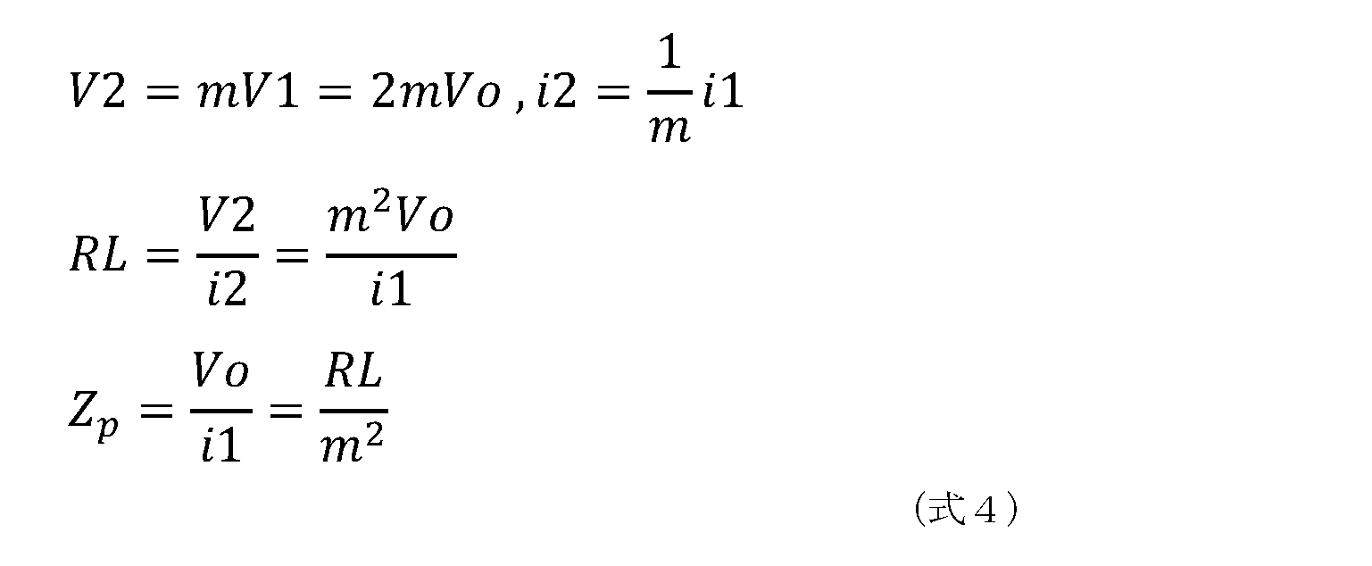
式3および式4に示されるように、大信号入力時に対して小信号入力時には、キャリアアンプ11の出力インピーダンスZpは2倍となっている。つまり、小信号入力時には、ピークアンプ12がオフ状態となり、キャリアアンプ11の出力インピーダンスZpが高くなることで、増幅回路500は高効率動作することが可能となる。
一方、大信号入力時には、キャリアアンプ11およびピークアンプ12が動作することで大電力信号を出力することができ、かつ、ピークアンプ12の出力インピーダンスZnが低いことで、信号歪を抑制することが可能となる。
1/4波長伝送線路530は、ピークアンプ12から出力される信号の位相を-90度シフトさせる(90度遅らせる)。1/4波長伝送線路530の配置により、キャリアアンプ11から出力された信号の位相とピークアンプ12から出力された信号の位相とが逆相となるように揃えられる。これにより、キャリアアンプ11から出力される信号と、ピークアンプ12から出力される信号とが、トランス20において電圧合成される。
図4は、従来の増幅回路500および実施の形態1に係る増幅回路10の増幅特性を比較したグラフである。図4において、横軸は信号出力端子200から出力される信号の電力レベルであり、縦軸は各増幅回路の効率(電力付加効率)である。
従来の増幅回路500では、キャリアアンプ11およびピークアンプ12の双方がAB級動作している増幅回路と比較して、低出力領域でのキャリアアンプ11の高インピーダンス動作、および、高出力領域でのピークアンプ12の低インピーダンス動作による低信号歪により、効率が改善されている。
これに対して、さらに、本実施の形態に係る増幅回路10では、増幅回路500と比較して、インピーダンス変換回路30による更なるキャリアアンプ11の高インピーダンス動作、および、高出力領域でのピークアンプ12の低インピーダンス動作により、高出力動作および中出力領域での効率が改善されている。
また、本実施の形態に係る高周波回路1では、1/4波長伝送線路530に代えて、1/4波長よりも短い線路で構成されたインピーダンス変換回路30が配置されているので、高周波回路1を小型化できる。
[1.4 効果など]
以上のように、本実施の形態に係る高周波回路1は、キャリアアンプ11およびピークアンプ12と、入力側コイル201および出力側コイル202を有するトランス20と、信号出力端子200と、インピーダンス変換回路30と、を備え、入力側コイル201の一端はキャリアアンプ11の出力端子に接続されており、出力側コイル202の一端は信号出力端子200に接続されており、出力側コイル202の他端はグランドに接続されており、インピーダンス変換回路30は、主線路301と、副線路302と、を有し、主線路301の一端31aはピークアンプ12の出力端子に接続されており、主線路301の他端31bは入力側コイル201の他端に接続されており、副線路302の一端32bは主線路301の一端31aに接続されており、副線路302の他端32aはグランドに接続されており、主線路301の一端31aから他端31bへ向かう第1方向と、副線路302の他端32aから一端32bへ向かう第2方向とは、同じである。
以上のように、本実施の形態に係る高周波回路1は、キャリアアンプ11およびピークアンプ12と、入力側コイル201および出力側コイル202を有するトランス20と、信号出力端子200と、インピーダンス変換回路30と、を備え、入力側コイル201の一端はキャリアアンプ11の出力端子に接続されており、出力側コイル202の一端は信号出力端子200に接続されており、出力側コイル202の他端はグランドに接続されており、インピーダンス変換回路30は、主線路301と、副線路302と、を有し、主線路301の一端31aはピークアンプ12の出力端子に接続されており、主線路301の他端31bは入力側コイル201の他端に接続されており、副線路302の一端32bは主線路301の一端31aに接続されており、副線路302の他端32aはグランドに接続されており、主線路301の一端31aから他端31bへ向かう第1方向と、副線路302の他端32aから一端32bへ向かう第2方向とは、同じである。
これによれば、1/4波長伝送線路に代えて、1/4波長よりも短い線路で構成されたインピーダンス変換回路30が配置されているので、高周波回路1を小型化できる。また、ピークアンプ12の出力インピーダンスを低減できるので、高出力領域で信号歪を低減できる。
また、本実施の形態に係る通信装置8は、高周波信号を処理するRFIC7と、RFIC7とアンテナ6との間で高周波信号を伝送する高周波回路1と、を備える。
これによれば、高周波回路1の効果を通信装置8で実現することができる。
(実施の形態2)
実施の形態1では、電圧合成型のドハティ増幅回路を示したが、本実施の形態では電流合成型のドハティ増幅回路を示す。
実施の形態1では、電圧合成型のドハティ増幅回路を示したが、本実施の形態では電流合成型のドハティ増幅回路を示す。
[2.高周波回路2および通信装置9の回路構成]
本実施の形態に係る高周波回路2および通信装置9の回路構成について、図5を参照しながら説明する。図5は、実施の形態2に係る高周波回路2および通信装置9の回路構成図である。
本実施の形態に係る高周波回路2および通信装置9の回路構成について、図5を参照しながら説明する。図5は、実施の形態2に係る高周波回路2および通信装置9の回路構成図である。
[2.1 通信装置9の回路構成]
まず、通信装置9の回路構成について説明する。図5に示すように、本実施の形態に係る通信装置9は、高周波回路2と、アンテナ6と、RFIC7と、を備える。本実施の形態に係る通信装置9は、実施の形態1に係る通信装置8と比較して、高周波回路2の構成のみが相違する。以下では、本実施の形態に係る通信装置9について、実施の形態1に係る通信装置8と異なる高周波回路2の構成について説明する。
まず、通信装置9の回路構成について説明する。図5に示すように、本実施の形態に係る通信装置9は、高周波回路2と、アンテナ6と、RFIC7と、を備える。本実施の形態に係る通信装置9は、実施の形態1に係る通信装置8と比較して、高周波回路2の構成のみが相違する。以下では、本実施の形態に係る通信装置9について、実施の形態1に係る通信装置8と異なる高周波回路2の構成について説明する。
[2.2 高周波回路2の回路構成]
図5に示すように、高周波回路2は、増幅回路50と、フィルタ82および83と、スイッチ81および84と、入力端子101と、アンテナ接続端子102と、を備える。本実施の形態に係る高周波回路2は、実施の形態1に係る高周波回路1と比較して、増幅回路50の構成のみが相違する。以下では、本実施の形態に係る高周波回路2について、増幅回路50の構成を中心に説明する。
図5に示すように、高周波回路2は、増幅回路50と、フィルタ82および83と、スイッチ81および84と、入力端子101と、アンテナ接続端子102と、を備える。本実施の形態に係る高周波回路2は、実施の形態1に係る高周波回路1と比較して、増幅回路50の構成のみが相違する。以下では、本実施の形態に係る高周波回路2について、増幅回路50の構成を中心に説明する。
増幅回路50は、入力端子101から入力されたバンドAおよびバンドBの送信信号を増幅する回路である。高周波回路2は、バンドAおよびバンドBのいずれかの高周波信号を、送信または受信することが可能である。さらに、高周波回路2は、バンドAおよびバンドBの高周波信号を、同時送信、同時受信、および同時送受信の少なくともいずれかで実行することも可能である。
なお、本発明に係る高周波回路2は、図5に示された回路構成のうち、増幅回路50を少なくとも有していればよい。
ここで、増幅回路50の回路構成について、詳細に説明する。
図5に示すように、増幅回路50は、キャリアアンプ11と、ピークアンプ12と、プリアンプ15と、移相回路70と、1/4波長伝送線路40と、インピーダンス変換回路30と、信号出力端子200と、を備える。
プリアンプ15および移相回路70については、実施の形態1に係る増幅回路10が備えるプリアンプ15および移相回路70と同じ構成および機能を有するので、ここでは説明を省略する。
キャリアアンプ11およびピークアンプ12のそれぞれは、増幅トランジスタを有する。上記増幅トランジスタは、例えば、HBT等のバイポーラトランジスタ、または、MOSFET等の電界効果トランジスタである。
キャリアアンプ11は、第1増幅素子の一例であり、信号RF1の全ての電力レベルに対して増幅動作可能なA級(またはAB級)増幅回路であり、特に、低出力領域および中出力領域において高効率な増幅動作が可能である。
ピークアンプ12は、第2増幅素子の一例であり、例えば、信号RF2の電力レベルが高い領域で増幅動作可能なC級増幅回路である。ピークアンプ12が有する増幅トランジスタには、キャリアアンプ11が有する増幅トランジスタに印加されるバイアス電圧よりも低いバイアス電圧が印加されているため、信号RF2の電力レベルが高くなるほど、出力インピーダンスが低くなる。これにより、ピークアンプ12は、高出力領域において低歪の増幅動作が可能である。
1/4波長伝送線路40は、第1伝送線路の一例であり、キャリアアンプ11の出力端子とピークアンプ12の出力端子との間に接続されている。1/4波長伝送線路40は、キャリアアンプ11から出力される信号の位相を-90度シフトさせる(90度遅らせる)。1/4波長伝送線路40の配置により、キャリアアンプ11から出力された信号の位相とピークアンプ12から出力された信号の位相とが揃えられる。これにより、キャリアアンプ11から出力される信号と、ピークアンプ12から出力される信号とが、電流合成される。
インピーダンス変換回路30は、第1回路の一例であり、主線路301と、副線路302と、を有し、インピーダンス変換回路30の両端で位相をシフトさせるとともに、所定の変換比でインピーダンスを変換する。主線路301は、第1主線路の一例であり、例えば、1/8波長または1/16波長の長さを有する伝送線路である。主線路301の一端31aは1/4波長伝送線路40の一端に接続されており、主線路301の他端31bは信号出力端子200に接続されている。1/4波長伝送線路40の他端は、キャリアアンプ11の出力端子に接続されている。副線路302は、第1副線路の一例であり、例えば、1/8波長または1/16波長の長さを有する伝送線路である。副線路302の一端32bは主線路301の一端31aに接続されており、副線路302の他端32aはグランドに接続されている。主線路301の一端31aから他端31bへ向かう第1方向と、副線路302の他端32aから一端32bへ向かう第2方向とは、同じである。上記構成において、主線路301と副線路302とは、電磁界結合している。なお、主線路301および副線路302の延伸方向に垂直な任意の方向から主線路301および副線路302を見た場合、上記第1方向と上記第2方向とは同じであることが望ましい。
増幅回路50の上記構成によれば、大信号入力時に対して小信号入力時には、キャリアアンプ11の出力インピーダンスは高くなる。つまり、小信号入力時には、ピークアンプ12がオフ状態となり、キャリアアンプ11の出力インピーダンスが高くなることで、増幅回路50は高効率動作することが可能となる。
一方、大信号入力時には、キャリアアンプ11およびピークアンプ12が動作することで大電力信号を出力することができ、かつ、ピークアンプ12の出力インピーダンスが低くなることで、信号歪を抑制することが可能となる。
また、本実施の形態に係る高周波回路2では、1/4波長伝送線路に代えて、1/4波長よりも短い線路で構成されたインピーダンス変換回路30が配置されているので、高周波回路2を小型化できる。
[2.3 変形例1に係る増幅回路51の回路構成および動作]
なお、本実施の形態に係る高周波回路2は、増幅回路50に代えて、変形例1に係る増幅回路51を備えてもよい。以下、変形例1に係る増幅回路51の回路構成および動作について説明する。図6Aは、実施の形態2の変形例1に係る増幅回路51の大信号入力時の回路状態図である。また、図6Bは、実施の形態2の変形例1に係る増幅回路51の小信号入力時の回路状態図である。
なお、本実施の形態に係る高周波回路2は、増幅回路50に代えて、変形例1に係る増幅回路51を備えてもよい。以下、変形例1に係る増幅回路51の回路構成および動作について説明する。図6Aは、実施の形態2の変形例1に係る増幅回路51の大信号入力時の回路状態図である。また、図6Bは、実施の形態2の変形例1に係る増幅回路51の小信号入力時の回路状態図である。
図6Aおよび6Bに示すように、変形例1に係る増幅回路51は、キャリアアンプ11と、ピークアンプ12と、1/4波長伝送線路40と、インピーダンス変換回路30および35と、信号出力端子200と、を備える。なお、図示していないが、増幅回路51は、プリアンプ15および移相回路70を備えてもよい。本変形例に係る増幅回路51は、実施の形態2に係る増幅回路50と比較して、インピーダンス変換回路35が付加されている点のみが異なる。以下、増幅回路51について、増幅回路50と同じ点については説明を省略し、異なる点を中心に説明する。
インピーダンス変換回路30は、第1回路の一例であり、主線路301と、副線路302と、を有し、インピーダンス変換回路30の両端で位相をシフトさせるとともに、所定の変換比でインピーダンスを変換する。主線路301は、第1主線路の一例であり、例えば、1/16波長の長さを有する伝送線路である。主線路301の一端31aは1/4波長伝送線路40の一端に接続されており、主線路301の他端31bは信号出力端子200に接続されている。1/4波長伝送線路40の他端は、キャリアアンプ11の出力端子に接続されている。副線路302は、第1副線路の一例であり、例えば、1/16波長の長さを有する伝送線路である。副線路302の一端32bは主線路301の一端31aに接続されており、副線路302の他端32aはグランドに接続されている。主線路301の一端31aから他端31bへ向かう第1方向と、副線路302の他端32aから一端32bへ向かう第2方向とは、同じである。上記構成において、主線路301と副線路302とは、電磁界結合している。なお、主線路301および副線路302の延伸方向に垂直な任意の方向から主線路301および副線路302を見た場合、上記第1方向と上記第2方向とは同じであることが望ましい。
インピーダンス変換回路35は、第2回路の一例であり、主線路351と、副線路352と、を有し、インピーダンス変換回路35の両端で位相をシフトさせるとともに、所定の変換比でインピーダンスを変換する。主線路351は、第2主線路の一例であり、例えば、1/16波長の長さを有する伝送線路である。主線路351の一端36aはピークアンプ12の出力端子に接続されており、主線路351の他端36bは1/4波長伝送線路40の一端および主線路301の一端31aに接続されている。副線路352は、第2副線路の一例であり、例えば、1/16波長の長さを有する伝送線路である。副線路352の一端37bは主線路351の一端36aに接続されており、副線路352の他端37aはグランドに接続されている。主線路351の一端36aから他端36bへ向かう第3方向と、副線路352の他端37aから一端37bへ向かう第4方向とは、同じである。上記構成において、主線路351と副線路352とは、電磁界結合している。なお、主線路351および副線路352の延伸方向に垂直な任意の方向から主線路351および副線路352を見た場合、上記第3方向と上記第4方向とは同じであることが望ましい。
次に、本変形例に係る増幅回路51の動作について説明する。
まず、図6Aに示すように、キャリアアンプ11およびピークアンプ12が動作(ON)している場合(大信号入力時)、キャリアアンプ11の出力インピーダンスZpおよびピークアンプ12の出力インピーダンスZnは、式5のように表される。なお、インピーダンス変換回路30は、インピーダンス変換回路30の出力端のインピーダンスに対して入力端のインピーダンスを1/nに変換するものとする。また、インピーダンス変換回路35は、インピーダンス変換回路35の出力端のインピーダンスに対して入力端のインピーダンスを1/nに変換するものとする。また、信号出力端子200に接続される負荷のインピーダンスをRLとする。式5に示すように、インピーダンス変換回路30および35により、ピークアンプ12の出力インピーダンスZnは、キャリアアンプ11の出力インピーダンスZpの1/nとなる。
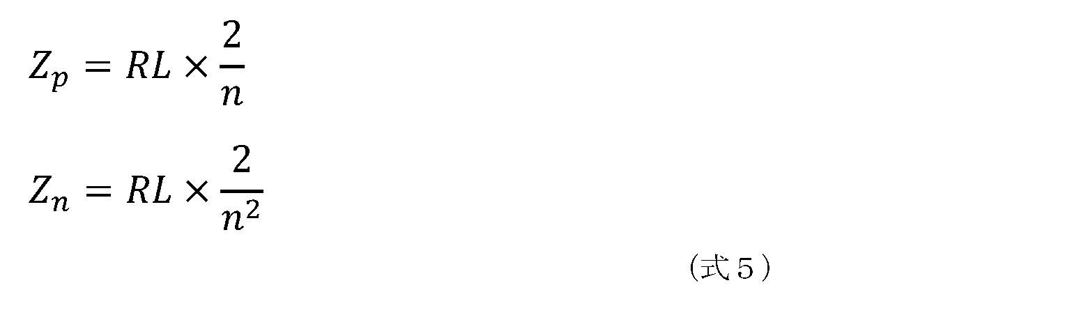
次に、図6Bに示すように、キャリアアンプ11が動作(ON)し、ピークアンプ12が動作していない(OFF)場合(小信号入力時)、キャリアアンプ11の出力インピーダンスZpは、式6のように表される。なお、このとき、ピークアンプ12の出力インピーダンスZnはオープン状態となっている。

式5および式6に示されるように、大信号入力時に対して小信号入力時には、キャリアアンプ11の出力インピーダンスZpは2倍となっている。つまり、小信号入力時には、ピークアンプ12がオフ状態となり、キャリアアンプ11の出力インピーダンスZpが高くなることで、増幅回路51は高効率動作することが可能となる。
一方、大信号入力時には、キャリアアンプ11およびピークアンプ12が動作することで大電力信号を出力することができ、かつ、インピーダンス変換回路35の配置により、実施の形態2に係る増幅回路50と比較して、ピークアンプ12の出力インピーダンスZnが低いことで、信号歪を抑制することが可能となる。
また、本変形例に係る増幅回路51では、1/4波長伝送線路に代えて、1/4波長よりも短い線路で構成されたインピーダンス変換回路30および35が配置されているので、増幅回路51を小型化できる。
[2.4 変形例2に係る増幅回路52の回路構成および動作]
なお、本実施の形態に係る高周波回路2は、増幅回路50に代えて、変形例2に係る増幅回路52を備えてもよい。以下、変形例2に係る増幅回路52の回路構成および動作について説明する。図7Aは、実施の形態2の変形例2に係る増幅回路52の大信号入力時の回路状態図である。また、図7Bは、実施の形態2の変形例2に係る増幅回路52の中信号入力時の回路状態図である。また、図7Cは、実施の形態2の変形例2に係る増幅回路52の小信号入力時の回路状態図である。
なお、本実施の形態に係る高周波回路2は、増幅回路50に代えて、変形例2に係る増幅回路52を備えてもよい。以下、変形例2に係る増幅回路52の回路構成および動作について説明する。図7Aは、実施の形態2の変形例2に係る増幅回路52の大信号入力時の回路状態図である。また、図7Bは、実施の形態2の変形例2に係る増幅回路52の中信号入力時の回路状態図である。また、図7Cは、実施の形態2の変形例2に係る増幅回路52の小信号入力時の回路状態図である。
図7A~7Cに示すように、変形例2に係る増幅回路52は、キャリアアンプ11および13と、ピークアンプ12と、1/4波長伝送線路40および41と、インピーダンス変換回路30および35と、信号出力端子200と、を備える。なお、図示していないが、増幅回路52は、プリアンプ15および移相回路70を備えてもよい。本変形例に係る増幅回路52は、実施の形態2の変形例1に係る増幅回路51と比較して、キャリアアンプ13および1/4波長伝送線路41が付加されている点のみが異なる。以下、増幅回路52について、増幅回路51と同じ点については説明を省略し、異なる点を中心に説明する。
キャリアアンプ13は、第3増幅素子の一例であり、端子130から入力される信号の全ての電力レベルに対して増幅動作可能なA級(またはAB級)増幅回路であり、特に、中出力領域において高効率な増幅動作が可能である。
1/4波長伝送線路41は、第2伝送線路の一例であり、1/4波長伝送線路41の一端は、キャリアアンプ13の出力端子に接続されており、1/4波長伝送線路41の他端は、ピークアンプ12の出力端子および主線路351の一端36aに接続されている。1/4波長伝送線路41は、キャリアアンプ13から出力される信号の位相を-90度シフトさせる(90度遅らせる)。1/4波長伝送線路41の配置により、キャリアアンプ13から出力された信号の位相とピークアンプ12から出力された信号の位相とが揃えられる。これにより、キャリアアンプ13から出力される信号と、ピークアンプ12から出力される信号とが、電流合成される。
次に、本変形例に係る増幅回路52の動作について説明する。
まず、図7Aに示すように、キャリアアンプ11および13、ならびにピークアンプ12が動作(ON)している場合(大信号入力時)、キャリアアンプ11の出力インピーダンスZp1、キャリアアンプ13の出力インピーダンスZp2、および、ピークアンプ12の出力インピーダンスZnは、式7のように表される。式7に示すように、インピーダンス変換回路30および35により、ピークアンプ12の出力インピーダンスZnは、キャリアアンプ11の出力インピーダンスZp1の2/nとなる。

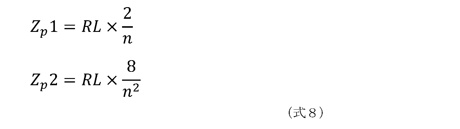
次に、図7Bに示すように、キャリアアンプ11および13が動作し(ON)し、ピークアンプ12が動作していない(OFF)場合(中信号入力時)、キャリアアンプ11の出力インピーダンスZp1およびキャリアアンプ13の出力インピーダンスZp2は、式8のように表される。なお、このとき、ピークアンプ12の出力インピーダンスZnはオープン状態となっている。式8に示すように、インピーダンス変換回路35により、キャリアアンプ13の出力インピーダンスZp2は、大信号入力時のキャリアアンプ13の出力インピーダンスZp2と比較して2倍となる。
次に、図7Cに示すように、キャリアアンプ11が動作(ON)し、キャリアアンプ13およびピークアンプ12が動作していない(OFF)場合(小信号入力時)、キャリアアンプ11の出力インピーダンスZp1は、式9のように表される。なお、このとき、キャリアアンプ13およびピークアンプ12の出力インピーダンスはオープン状態となっている。

式9に示されるように、中信号入力時に対して小信号入力時には、キャリアアンプ11の出力インピーダンスZp1は2倍となっている。つまり、小信号入力時には、キャリアアンプ13およびピークアンプ12がオフ状態となり、キャリアアンプ11の出力インピーダンスZp1が高くなることで、増幅回路52は高効率動作することが可能となる。
一方、大信号入力時には、キャリアアンプ11および13、ならびにピークアンプ12が動作することで大電力信号を出力することができ、かつ、ピークアンプ12の出力インピーダンスZnが低いことで、信号歪を抑制することが可能となる。
増幅回路52の上記構成によれば、大信号入力時、中信号入力時および小信号入力時へと遷移するにつれて、キャリアアンプ11の出力インピーダンスZp1は高くなる。
つまり、本変形例に係る増幅回路52によれば、変形例1に係る増幅回路51と比較して、大信号出力時、中信号入力時および小信号入力時に応じてキャリアアンプ11および13の出力インピーダンスを細かく設定できるので、効率をより高精度に向上させることが可能となる。
[2.5 高周波回路2の部品配置構成]
次に、実施の形態2に係る高周波回路2の部品実装構成について説明する。
次に、実施の形態2に係る高周波回路2の部品実装構成について説明する。
図8は、実施の形態2に係る高周波回路2の平面図および断面図である。図8の(a)には、基板60の主面をz軸正方向側から見た場合の回路部品の配置を透視した図が示され、図8の(b)には、図8の(a)のVIIIB-VIIIB線における断面図が示されている。また、図8の(a)では、各回路部品の配置関係が容易に理解されるよう各回路部品にはその機能を表すマークが付されている場合があるが、実際の各回路部品には、当該マークは付されていない。また、図8において、基板60および各回路部品を接続する配線の図示が省略されている。
なお、高周波回路2は、さらに、基板60の表面および回路部品の一部を覆う樹脂部材、ならびに、樹脂部材の表面を覆うシールド電極層を備えてもよいが、図8では、樹脂部材およびシールド電極層の図示が省略されている。
高周波回路2は、図5に示された回路構成に加えて、さらに、基板60および電源線路90を有している。
基板60は、高周波回路2を構成する回路部品を実装する基板である。基板60としては、例えば、複数の誘電体層の積層構造を有する低温同時焼成セラミックス(Low Temperature Co-fired Ceramics:LTCC)基板、高温同時焼成セラミックス(High Temperature Co-fired Ceramics:HTCC)基板、部品内蔵基板、再配線層(Redistribution Layer:RDL)を有する基板、または、プリント基板等が用いられる。
基板60の表面上には、キャリアアンプ11およびピークアンプ12、および容量素子などが配置されている。
キャリアアンプ11および13は、半導体ICに含まれている。半導体ICは、基板60上に配置されている。半導体ICは、例えばCMOS(Complementary Metal Oxide Semiconductor)を用いて構成され、具体的にはSOI(Silicon on Insulator)プロセスにより製造されてもよい。また、半導体ICは、GaAs、SiGe及びGaNのうちの少なくとも1つで構成されてもよい。なお、半導体ICの半導体材料は、上述した材料に限定されない。なお、プリアンプ15、移相回路70、スイッチ81および84の少なくともいずれかは、半導体ICに含まれていてもよい。
基板60の表面または内部には、インピーダンス変換回路30の主線路301および副線路302(図示せず)が形成されている。主線路301および副線路302は、基板60の表面または内部に形成された平面導体で構成されている。主線路301と副線路302とは、基板60の同層に形成されてもよいし、また、別層に形成されてもよい。また、主線路301および副線路302のそれぞれは、複数層にわたって形成されていてもよい。
電源線路90は、キャリアアンプ11およびピークアンプ12に接続され、キャリアアンプ11およびピークアンプ12に電源電圧を供給するための配線である。電源線路90は、基板60の表面または内部に形成されている。電源線路90は、基板60の表面または内部に形成された平面導体で構成されている。
ここで、基板60を平面視した場合、主線路301および副線路302は、基板60の表面または内部であってピークアンプ12の第5方向(図8のy軸方向)に配置されている。これに対して、電源線路90は、基板60の表面または内部であってキャリアアンプ11の第5方向(図8のy軸方向)と、主線路301および副線路302の第5方向と直交する第6方向(図8のx軸方向)との交差部分に配置されている。
これによれば、主線路301および副線路302とピークアンプ12との距離を小さくでき、かつ、上記交差部分のスペースを有効活用して電源線路90を配置できる。よって、高周波回路2の伝送損失を低減しつつ高周波回路2を小型化できる。
[2.6 効果など]
以上のように、本実施の形態に係る高周波回路2は、キャリアアンプ11およびピークアンプ12と、1/4波長伝送線路40と、信号出力端子200と、インピーダンス変換回路30と、を備え、1/4波長伝送線路40は、キャリアアンプ11の出力端子とピークアンプ12の出力端子との間に接続されており、インピーダンス変換回路30は、主線路301と、副線路302と、を有し、主線路301の一端31aは1/4波長伝送線路40の一端に接続されており、主線路301の他端31bは信号出力端子200に接続されており、1/4波長伝送線路40の他端は、キャリアアンプ11の出力端子に接続されており、副線路302の一端32bは主線路301の一端31aに接続されており、副線路302の他端32aはグランドに接続されており、主線路301の一端31aから他端31bへ向かう第1方向と、副線路302の他端32aから一端32bへ向かう第2方向とは、同じである。
以上のように、本実施の形態に係る高周波回路2は、キャリアアンプ11およびピークアンプ12と、1/4波長伝送線路40と、信号出力端子200と、インピーダンス変換回路30と、を備え、1/4波長伝送線路40は、キャリアアンプ11の出力端子とピークアンプ12の出力端子との間に接続されており、インピーダンス変換回路30は、主線路301と、副線路302と、を有し、主線路301の一端31aは1/4波長伝送線路40の一端に接続されており、主線路301の他端31bは信号出力端子200に接続されており、1/4波長伝送線路40の他端は、キャリアアンプ11の出力端子に接続されており、副線路302の一端32bは主線路301の一端31aに接続されており、副線路302の他端32aはグランドに接続されており、主線路301の一端31aから他端31bへ向かう第1方向と、副線路302の他端32aから一端32bへ向かう第2方向とは、同じである。
これによれば、1/4波長伝送線路に代えて、1/4波長よりも短い線路で構成されたインピーダンス変換回路30が配置されているので、高周波回路2を小型化できる。
また例えば、高周波回路2は、さらに、インピーダンス変換回路35を備え、インピーダンス変換回路35は、主線路351と、副線路352と、を有し、主線路351の一端36aはピークアンプ12の出力端子に接続されており、主線路351の他端は1/4波長伝送線路40の一端および主線路301の一端31aに接続されており、副線路352の一端37bは主線路351の一端36aに接続されており、副線路352の他端はグランドに接続されており、主線路351の一端36aから他端36bへ向かう第3方向と、副線路352の他端37aから一端37bへ向かう第4方向とは、同じであってもよい。
これによれば、1/4波長伝送線路に代えて、1/4波長よりも短い線路で構成されたインピーダンス変換回路30および35が配置されているので、高周波回路2を小型化できる。また、ピークアンプ12の出力インピーダンスを低減できるので、高出力領域で信号歪を低減できる。
また例えば、高周波回路2は、さらに、キャリアアンプ13と、1/4波長伝送線路41と、を備え、1/4波長伝送線路41の一端はキャリアアンプ13の出力端子に接続されており、1/4波長伝送線路41の他端はピークアンプ12の出力端子および主線路351の一端36aに接続されていてもよい。
これによれば、低出力領域および中出力領域において、キャリアアンプ13の出力インピーダンスを高くできるので、高効率化が促進される。
また例えば、高周波回路2は、さらに、基板60と、キャリアアンプ11およびピークアンプ12に接続され、キャリアアンプ11およびピークアンプ12に電源電圧を供給するための電源線路90と、を備え、キャリアアンプ11およびピークアンプ12は、基板60上または内部に配置され、基板60を平面視した場合、主線路301および副線路302は、基板60の表面または内部であってピークアンプ12の第5方向に配置されており、電源線路90は、基板60の表面または内部であってキャリアアンプ11の第5方向と、主線路301および副線路302の第5方向と直交する第6方向との交差部分に配置されていてもよい。
これによれば、主線路301および副線路302とピークアンプ12との距離を小さくでき、かつ、上記交差部分のスペースを有効活用して電源線路90を配置できる。よって、高周波回路2の伝送損失を低減しつつ高周波回路2を小型化できる。
また例えば、高周波回路2において、キャリアアンプ11およびピークアンプ12は、半導体ICに含まれており、当該半導体ICは基板60上に配置されていてもよい。
これによれば、高周波回路2を小型化できる。
また、本実施の形態に係る通信装置9は、高周波信号を処理するRFIC7と、RFIC7とアンテナ6との間で高周波信号を伝送する高周波回路2と、を備える。
これによれば、高周波回路2の効果を通信装置9で実現することができる。
(その他の実施の形態など)
以上、本発明の実施の形態に係る高周波回路および通信装置について、実施の形態および変形例を挙げて説明したが、本発明に係る高周波回路および通信装置は、上記実施の形態および変形例に限定されるものではない。上記実施の形態および変形例における任意の構成要素を組み合わせて実現される別の実施の形態や、上記実施の形態および変形例に対して本発明の主旨を逸脱しない範囲で当業者が思いつく各種変形を施して得られる変形例や、上記高周波回路および通信装置を内蔵した各種機器も本発明に含まれる。
以上、本発明の実施の形態に係る高周波回路および通信装置について、実施の形態および変形例を挙げて説明したが、本発明に係る高周波回路および通信装置は、上記実施の形態および変形例に限定されるものではない。上記実施の形態および変形例における任意の構成要素を組み合わせて実現される別の実施の形態や、上記実施の形態および変形例に対して本発明の主旨を逸脱しない範囲で当業者が思いつく各種変形を施して得られる変形例や、上記高周波回路および通信装置を内蔵した各種機器も本発明に含まれる。
例えば、上記実施の形態および変形例に係る高周波回路および通信装置において、図面に開示された各回路素子および信号経路を接続する経路の間に、別の回路素子および配線などが挿入されていてもよい。
本発明は、マルチバンド対応のフロントエンド部に配置される高周波回路として、携帯電話などの通信機器に広く利用できる。
1、2 高周波回路
6 アンテナ
7 RF信号処理回路(RFIC)
8、9 通信装置
10、50、51、52、500 増幅回路
11、13 キャリアアンプ
12 ピークアンプ
15 プリアンプ
20 トランス
30、35 インピーダンス変換回路
31a、32b、36a、37b 一端
31b、32a、36b、37a 他端
40、41、530 1/4波長伝送線路
60 基板
70 移相回路
81、84 スイッチ
82、83 フィルタ
90 電源線路
101 入力端子
102 アンテナ接続端子
110、120、130 端子
200 信号出力端子
201 入力側コイル
202 出力側コイル
301、351 主線路
302、352 副線路
6 アンテナ
7 RF信号処理回路(RFIC)
8、9 通信装置
10、50、51、52、500 増幅回路
11、13 キャリアアンプ
12 ピークアンプ
15 プリアンプ
20 トランス
30、35 インピーダンス変換回路
31a、32b、36a、37b 一端
31b、32a、36b、37a 他端
40、41、530 1/4波長伝送線路
60 基板
70 移相回路
81、84 スイッチ
82、83 フィルタ
90 電源線路
101 入力端子
102 アンテナ接続端子
110、120、130 端子
200 信号出力端子
201 入力側コイル
202 出力側コイル
301、351 主線路
302、352 副線路
Claims (7)
- 第1増幅素子および第2増幅素子と、
入力側コイルおよび出力側コイルを有するトランスと、
信号出力端子と、
第1回路と、を備え、
前記入力側コイルの一端は、前記第1増幅素子の出力端子に接続されており、
前記出力側コイルの一端は、前記信号出力端子に接続されており、
前記出力側コイルの他端は、グランドに接続されており、
前記第1回路は、
第1主線路と、
第1副線路と、を有し、
前記第1主線路の一端は、前記第2増幅素子の出力端子に接続されており、前記第1主線路の他端は、前記入力側コイルの他端に接続されており、
前記第1副線路の一端は、前記第1主線路の前記一端に接続されており、前記第1副線路の他端は、グランドに接続されており、
前記第1主線路の前記一端から前記他端へ向かう第1方向と、前記第1副線路の前記他端から前記一端へ向かう第2方向とは、同じである、
高周波回路。 - 第1増幅素子および第2増幅素子と、
第1伝送線路と、
信号出力端子と、
第1回路と、を備え、
前記第1伝送線路は、前記第1増幅素子の出力端子と前記第2増幅素子の出力端子との間に接続されており、
前記第1回路は、
第1主線路と、
第1副線路と、を有し、
前記第1主線路の一端は、前記第1伝送線路の一端に接続されており、前記第1主線路の他端は、前記信号出力端子に接続されており、
前記第1伝送線路の他端は、前記第1増幅素子の出力端子に接続されており、
前記第1副線路の一端は、前記第1主線路の前記一端に接続されており、前記第1副線路の他端は、グランドに接続されており、
前記第1主線路の前記一端から前記他端へ向かう第1方向と、前記第1副線路の前記他端から前記一端へ向かう第2方向とは、同じである、
高周波回路。 - さらに、
第2回路を備え、
前記第2回路は、
第2主線路と、
第2副線路と、を有し、
前記第2主線路の一端は、前記第2増幅素子の出力端子に接続されており、前記第2主線路の他端は、前記第1伝送線路の前記一端および前記第1主線路の前記一端に接続されており、
前記第2副線路の一端は、前記第2主線路の前記一端に接続されており、前記第2副線路の他端は、グランドに接続されており、
前記第2主線路の前記一端から前記他端へ向かう第3方向と、前記第2副線路の前記他端から前記一端へ向かう第4方向とは、同じである、
請求項2に記載の高周波回路。 - さらに、
第3増幅素子と、
第2伝送線路と、を備え、
前記第2伝送線路の一端は、前記第3増幅素子の出力端子に接続されており、前記第2伝送線路の他端は、前記第2増幅素子の出力端子および前記第2主線路の前記一端に接続されている、
請求項3に記載の高周波回路。 - さらに、
基板と、
前記第1増幅素子および前記第2増幅素子に接続され、前記第1増幅素子および前記第2増幅素子に電源電圧を供給するための電源線路と、を備え、
前記第1増幅素子および前記第2増幅素子は、前記基板上または内部に配置され、
前記基板を平面視した場合、
前記第1主線路および前記第1副線路は、前記基板の表面または内部であって前記第2増幅素子の第5方向に配置されており、
前記電源線路は、前記基板の表面または内部であって前記第1増幅素子の前記第5方向と、前記第1主線路および前記第1副線路の前記第5方向と直交する第6方向との交差部分に配置されている、
請求項2~4のいずれか1項に記載の高周波回路。 - 前記第1増幅素子および前記第2増幅素子は、半導体ICに含まれており、
前記半導体ICは、前記基板上に配置されている、
請求項5に記載の高周波回路。 - 高周波信号を処理する信号処理回路と、
前記信号処理回路とアンテナとの間で前記高周波信号を伝送する、請求項1~6のいずれか1項に記載の高周波回路と、を備える、
通信装置。
Priority Applications (2)
| Application Number | Priority Date | Filing Date | Title |
|---|---|---|---|
| CN202280039154.4A CN117413459A (zh) | 2021-06-02 | 2022-05-31 | 高频电路和通信装置 |
| US18/520,587 US20240097626A1 (en) | 2021-06-02 | 2023-11-28 | Radio frequency circuit and communication device |
Applications Claiming Priority (2)
| Application Number | Priority Date | Filing Date | Title |
|---|---|---|---|
| JP2021-093181 | 2021-06-02 | ||
| JP2021093181 | 2021-06-02 |
Related Child Applications (1)
| Application Number | Title | Priority Date | Filing Date |
|---|---|---|---|
| US18/520,587 Continuation US20240097626A1 (en) | 2021-06-02 | 2023-11-28 | Radio frequency circuit and communication device |
Publications (1)
| Publication Number | Publication Date |
|---|---|
| WO2022255388A1 true WO2022255388A1 (ja) | 2022-12-08 |
Family
ID=84323431
Family Applications (1)
| Application Number | Title | Priority Date | Filing Date |
|---|---|---|---|
| PCT/JP2022/022226 Ceased WO2022255388A1 (ja) | 2021-06-02 | 2022-05-31 | 高周波回路および通信装置 |
Country Status (3)
| Country | Link |
|---|---|
| US (1) | US20240097626A1 (ja) |
| CN (1) | CN117413459A (ja) |
| WO (1) | WO2022255388A1 (ja) |
Families Citing this family (1)
| Publication number | Priority date | Publication date | Assignee | Title |
|---|---|---|---|---|
| US20230308062A1 (en) * | 2022-03-23 | 2023-09-28 | Qorvo Us, Inc. | High power back-off efficiency asymmetric-stacked differential quadrature load modulation pa |
Citations (5)
| Publication number | Priority date | Publication date | Assignee | Title |
|---|---|---|---|---|
| JP2006525751A (ja) * | 2003-05-05 | 2006-11-09 | クリー マイクロウエイブ リミテッド ライアビリティ カンパニー | 選択された位相長および出力インピーダンスを用いた増加されたバックオフ能力および電力付加効率を持つnウェイrf電力増幅器回路 |
| JP2011244070A (ja) * | 2010-05-14 | 2011-12-01 | Hitachi Ltd | 電力増幅器及びそれを用いた基地局 |
| JP2013085179A (ja) * | 2011-10-12 | 2013-05-09 | Toshiba Corp | 電力増幅回路、および無線通信装置 |
| CN108768308A (zh) * | 2018-05-16 | 2018-11-06 | 清华大学 | 基于晶体管堆叠结构的非对称Doherty功率放大器 |
| JP2020038957A (ja) * | 2018-09-03 | 2020-03-12 | 株式会社村田製作所 | 伝送線路トランス及び増幅回路 |
-
2022
- 2022-05-31 WO PCT/JP2022/022226 patent/WO2022255388A1/ja not_active Ceased
- 2022-05-31 CN CN202280039154.4A patent/CN117413459A/zh active Pending
-
2023
- 2023-11-28 US US18/520,587 patent/US20240097626A1/en active Pending
Patent Citations (5)
| Publication number | Priority date | Publication date | Assignee | Title |
|---|---|---|---|---|
| JP2006525751A (ja) * | 2003-05-05 | 2006-11-09 | クリー マイクロウエイブ リミテッド ライアビリティ カンパニー | 選択された位相長および出力インピーダンスを用いた増加されたバックオフ能力および電力付加効率を持つnウェイrf電力増幅器回路 |
| JP2011244070A (ja) * | 2010-05-14 | 2011-12-01 | Hitachi Ltd | 電力増幅器及びそれを用いた基地局 |
| JP2013085179A (ja) * | 2011-10-12 | 2013-05-09 | Toshiba Corp | 電力増幅回路、および無線通信装置 |
| CN108768308A (zh) * | 2018-05-16 | 2018-11-06 | 清华大学 | 基于晶体管堆叠结构的非对称Doherty功率放大器 |
| JP2020038957A (ja) * | 2018-09-03 | 2020-03-12 | 株式会社村田製作所 | 伝送線路トランス及び増幅回路 |
Also Published As
| Publication number | Publication date |
|---|---|
| CN117413459A (zh) | 2024-01-16 |
| US20240097626A1 (en) | 2024-03-21 |
Similar Documents
| Publication | Publication Date | Title |
|---|---|---|
| WO2023007996A1 (ja) | 電力増幅回路および通信装置 | |
| US20240405735A1 (en) | Radio-frequency circuit and communication device | |
| US20240429871A1 (en) | High-frequency module and communication device | |
| US20260045915A1 (en) | Amplifier circuit | |
| US20250088161A1 (en) | Amplifier circuit and communication device | |
| US20240178868A1 (en) | Radio frequency circuit, communication device, and power amplification method for radio frequency circuit | |
| US20240405732A1 (en) | High frequency circuit and communication apparatus | |
| US20240146258A1 (en) | Power amplifier circuit and power amplification method | |
| WO2022255388A1 (ja) | 高周波回路および通信装置 | |
| US20250023588A1 (en) | High frequency circuit and communication device | |
| WO2023008255A1 (ja) | 高周波回路および通信装置 | |
| US12580538B2 (en) | Radio-frequency module and communication apparatus | |
| US20240204739A1 (en) | Radio frequency circuit and communication device | |
| US20250266854A1 (en) | Radio-frequency circuit | |
| WO2022091830A1 (ja) | 高周波モジュールおよび通信装置 | |
| WO2022254875A1 (ja) | 高周波回路および通信装置 | |
| US20240113668A1 (en) | Amplifier circuit and radio frequency circuit | |
| US20250047250A1 (en) | Radio frequency circuit and communication device | |
| US20250266796A1 (en) | Radio-frequency circuit | |
| WO2026018520A1 (ja) | 増幅回路 | |
| CN118140413A (zh) | 高频电路和通信装置 | |
| CN117378141A (zh) | 高频电路和通信装置 |
Legal Events
| Date | Code | Title | Description |
|---|---|---|---|
| 121 | Ep: the epo has been informed by wipo that ep was designated in this application |
Ref document number: 22816134 Country of ref document: EP Kind code of ref document: A1 |
|
| WWE | Wipo information: entry into national phase |
Ref document number: 202280039154.4 Country of ref document: CN |
|
| NENP | Non-entry into the national phase |
Ref country code: DE |
|
| 122 | Ep: pct application non-entry in european phase |
Ref document number: 22816134 Country of ref document: EP Kind code of ref document: A1 |
|
| NENP | Non-entry into the national phase |
Ref country code: JP |