WO2022255008A1 - ゲート駆動装置 - Google Patents
ゲート駆動装置 Download PDFInfo
- Publication number
- WO2022255008A1 WO2022255008A1 PCT/JP2022/018895 JP2022018895W WO2022255008A1 WO 2022255008 A1 WO2022255008 A1 WO 2022255008A1 JP 2022018895 W JP2022018895 W JP 2022018895W WO 2022255008 A1 WO2022255008 A1 WO 2022255008A1
- Authority
- WO
- WIPO (PCT)
- Prior art keywords
- circuit
- voltage
- sense
- current
- gate
- Prior art date
- Legal status (The legal status is an assumption and is not a legal conclusion. Google has not performed a legal analysis and makes no representation as to the accuracy of the status listed.)
- Ceased
Links
Images


Classifications
-
- H—ELECTRICITY
- H02—GENERATION; CONVERSION OR DISTRIBUTION OF ELECTRIC POWER
- H02M—APPARATUS FOR CONVERSION BETWEEN AC AND AC, BETWEEN AC AND DC, OR BETWEEN DC AND DC, AND FOR USE WITH MAINS OR SIMILAR POWER SUPPLY SYSTEMS; CONVERSION OF DC OR AC INPUT POWER INTO SURGE OUTPUT POWER; CONTROL OR REGULATION THEREOF
- H02M1/00—Details of apparatus for conversion
- H02M1/08—Circuits specially adapted for the generation of control voltages for semiconductor devices incorporated in static converters
-
- H—ELECTRICITY
- H03—ELECTRONIC CIRCUITRY
- H03K—PULSE TECHNIQUE
- H03K17/00—Electronic switching or gating, i.e. not by contact-making and –breaking
- H03K17/08—Modifications for protecting switching circuit against overcurrent or overvoltage
Definitions
- the present disclosure relates to a gate drive device.
- semiconductor switching elements tend to have a lower saturation current during a short circuit as they become smaller.
- the difference between the current sense value and the normal current sense value becomes smaller, and considering the variation in these values, the two may overlap, making it impossible to set the threshold value and making correct judgments. rice field.
- An object of the present disclosure is to provide a gate drive device that can reliably determine the short-circuit state of the opposed arm even when the short-circuit saturation current is reduced due to the progress of miniaturization of semiconductor switching elements.
- a gate drive device is a gate drive device that performs drive control of a gate-driven semiconductor switching element having a current sense terminal, and captures a sense current detection signal from the current sense terminal.
- a waveform detection circuit for detecting the presence or absence of a transient sense current from changes in the sense current; a judgment circuit for judging the presence or absence of a short circuit by judging the detection result of the waveform detection circuit at a predetermined timing; and a control circuit that controls the drive, turns on the semiconductor switching element, and then shuts off when the determination circuit determines that there is a short circuit.
- the waveform detection circuit captures the sense current detection signal from the current sense terminal of the semiconductor switching element, detects the presence or absence of a transient sense current from changes in the waveform of the sense current, and detects the presence or absence of a short circuit.
- the short-circuit state can be determined at a predetermined timing by the determination circuit.
- FIG. 1 is an electrical configuration diagram showing the first embodiment
- FIG. 2 is the action explanatory diagram 1 showing the first embodiment
- FIG. 3 is a timing chart showing the first embodiment
- FIG. 4 is the action explanatory diagram part 2 showing the first embodiment
- FIG. 5 is the action explanatory diagram No. 3 showing the first embodiment
- FIG. 6 is the operation explanatory diagram No. 4 showing the first embodiment
- FIG. 7 is the action explanatory diagram No. 5 showing the first embodiment
- FIG. 8 is an electrical configuration diagram showing the second embodiment
- FIG. 9 is a timing chart showing the second embodiment
- FIG. 10 is an electrical configuration diagram showing the third embodiment
- FIG. 11 is a timing chart showing the third embodiment
- FIG. 12 is an electrical configuration diagram showing a fourth embodiment
- FIG. 13 is the action explanatory diagram No. 1 showing the fourth embodiment
- FIG. 14 is the action explanatory diagram part 2 showing the fourth embodiment
- FIG. 15 is the action explanatory diagram 3 showing the fourth embodiment
- FIG. 16 is an electrical configuration diagram showing a fifth embodiment
- FIG. 17 is a timing chart showing the fifth embodiment
- FIG. 18 is an electrical configuration diagram showing the sixth embodiment
- FIG. 19 is an operation explanatory diagram showing the sixth embodiment
- FIG. 20 is an electrical configuration diagram showing the seventh embodiment
- FIG. 21 is an operation explanatory diagram showing the seventh embodiment
- FIG. 22 is an electrical configuration diagram showing the eighth embodiment
- FIG. 23 is a timing chart showing the eighth embodiment
- FIG. 24 is a timing chart showing the ninth embodiment.
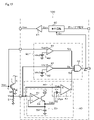
- FIG. 1 showing the electrical configuration, for a circuit in which IGBTs 1 as gate-driven semiconductor switching elements are arranged on upper and lower arms to form current paths to a load, a gate drive device 10 has one of the IGBTs 1 It has a function to determine whether or not the other IGBT is in a short-circuited state during on-drive control.
- IGBT is an abbreviation for Insulated Gate Bipolar Transistor.
- the IGBT 1 is provided with a sense element for detecting current between the collector and the emitter, and has a sense terminal SE serving as an output terminal for the sense current.
- the sense terminal SE is commonly connected to the emitter via a current detection resistor 2, and the gate drive device 10 is provided to receive the sense current Ise flowing through the current detection resistor 2 as a sense voltage Vse.
- the gate drive device 10 includes a control circuit 20, a determination circuit 30 and a waveform detection circuit 40.
- the control circuit 20 generates a gate drive signal Son based on an externally applied on/off command signal, and applies a gate drive voltage Von to the gate of the IGBT 1 via the drive circuit 21 .
- the control circuit 20 also has an off-driving function for the IGBT 1, and cuts off the IGBT 1 when a short circuit is detected during on-driving.
- the determination circuit 30 includes a comparator 31, a threshold voltage source 32, a delay circuit 33 and an AND circuit 34.
- the determination circuit 30 determines the state of the IGBT 1 when a predetermined delay time Td1 elapses after the gate voltage Vge of the IGBT 1 reaches the threshold voltage Vth1 and the IGBT 1 is turned on.
- the gate voltage Vge of the IGBT 1 is input to the non-inverting input terminal of the comparator 31, and the threshold voltage Vth1 set by the threshold voltage source 32 is input to the inverting input terminal.
- the delay circuit 33 is triggered by the on-timing signal output from the comparator 31, and outputs a high-level signal to the AND circuit 34 after a predetermined delay time Td1.
- the AND circuit 34 determines the output signal from the waveform detection circuit 40 at the input timing of the high level signal from the delay circuit 33, and outputs a determination signal Sx in the case of a short circuit state.
- the waveform detection circuit 40 includes a peak hold circuit 50 and a comparison circuit 60 consisting of a comparator with hysteresis.
- the waveform detection circuit 40 takes in the sense voltage Vse, detects an abnormal state from the changing state of this waveform, and outputs it.
- the peak hold circuit 50 includes an operational amplifier 51, a transistor 52 and a capacitor 53.
- the operational amplifier 51 has a non-inverting input terminal to which the sense voltage Vse is input, and an inverting input terminal to which the terminal voltage Vph of the capacitor 53 is input.
- the output terminal of operational amplifier 51 is connected to the base of transistor 52 .
- the collector of the transistor 52 is connected to the DC power supply VD, and the emitter is connected to the ground through the capacitor 53.
- a peak hold voltage Vph which is the terminal voltage of the capacitor 53 , is the voltage at the common connection point between the emitter of the transistor 52 and the capacitor 53 .
- the operational amplifier 51 drives the transistor 52 and charges the capacitor 53 from the DC power supply VD during the period when the sense voltage Vse is higher than the peak hold voltage Vph which is the terminal voltage of the capacitor 53 .
- the output signal of the operational amplifier 51 turns off the transistor 52 and stops charging the capacitor 53 .
- the peak hold voltage Vph becomes the peak value VP of the sense voltage Vse, and this voltage is held.
- the comparison circuit 60 includes a comparator 61 and a hysteresis power supply 62 that provides a hysteresis voltage Vh.
- the comparator 61 has a non-inverting input terminal to which the sense voltage Vse is input, and an inverting input terminal to which the peak hold voltage Vph output from the peak hold circuit 50 is lowered by the hysteresis voltage Vh through the hysteresis power supply 62 and input as a reference voltage Vhys. be.
- the comparator 61 outputs a detection signal Sd that becomes high level when the sense voltage Vse is greater than the reference voltage Vhys and becomes low level when it becomes smaller than the reference voltage Vhys.
- This detection signal Sd is input to the AND circuit 34 of the determination circuit 30 .
- FIG. 6 shows a configuration in which two IGBT_A and IGBT_B are arranged in the upper and lower arms, and the dashed line with an arrow indicates the current that flows from turning off the IGBT_A of the upper arm to turning on the IGBT_B of the lower arm.
- the upper side shows the current when the IGBT_A of the upper arm is normal, and the lower side shows the current when the IGBT_A is in a short circuit state.
- the current I2 flowing through the IGBT_B flows as a current obtained by adding the recovery current I1r of the body diode to the current I1f flowing through the body diode from the load side. Therefore, when the IGBT_B is turned on, a current with a peak due to the recovery current is generated in the transient period, and reaches the level of the load current in the stationary period.
- the short-circuit current I1s flowing through the IGBT_A now flows through the IGBT_B as the current I2. Further, since almost no current flows through the body diode of IGBT_A, no recovery current is generated, and the current I2 does not have a peak value due to the recovery current.
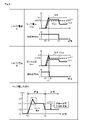
- FIG. 7 is a timing chart showing the above operation as signal changes of each part. Gate voltage Vge, collector current Ic, sense voltage Vse, and collector voltage Vce in normal and short-circuited states are shown.
- the gate voltage of the IGBT is raised to the gate voltage VGE after being held at the mirror voltage Vm during the transition period. At this time, when the gate voltage Vge reaches the threshold voltage Vth at the time t0, the collector current Ic flows according to the load.
- the sense voltage Vse which indicates the change in the sense current Ise, increases from 0 V with the on-drive, and after passing the peak value due to the recovery current, it operates in the saturation region in the transitional period, so it maintains the voltage V2 higher than in the steady period. . After that, when shifting to the stationary period, the sense voltage Vse enters the linear region, so it drops to the voltage V1 proportional to the load current, and this state is maintained during the ON period. Also, the collector voltage Vce begins to gradually decrease from the power supply voltage VCE in the transitional period, and reaches approximately 0V in the stationary period.
- the gate voltage of the IGBT rises to the gate voltage VGE regardless of the mirror period.
- the collector current Ic rises to the short-circuit current level due to the power short-circuit state.
- the sense voltage Vse increases from 0 V with on-driving, operates in the saturation region without recovery current, and reaches a high voltage V3 level corresponding to the short-circuit current. Also, the collector voltage Vce remains in the state where the power supply voltage VCE is applied.
- FIG. 2 shows the states of the sense voltage Vse and the detection signal Sd during normal operation and short circuit.
- the sense voltage Vse rises to a level corresponding to the short-circuit current flowing through the IGBT1, and this level is maintained. Therefore, the sense voltage Vse is held at the peak value VP itself and does not drop below this value.
- FIG. 3 shows a timing chart when the gate drive device 10 receives an ON/OFF command signal from the outside and applies the gate drive voltage Von to the gate of the IGBT 1 .
- the control circuit 20 applies the gate drive voltage Von to the IGBT 1 through the drive circuit 21, the gate voltage Vge of the IGBT 1 rises when the IGBT of the opposite arm is normal, and at time t0.
- the threshold voltage Vth1 is reached, the current begins to flow and the transition period is entered.
- the determination circuit 30 outputs a high-level signal to the delay circuit 33 because the gate voltage Vge input to the comparator 31 has reached the threshold voltage Vth1.
- the delay circuit 33 outputs a high-level timing signal to the AND circuit 34 at time t3 when a predetermined delay time td1 has elapsed from time t0 when the high-level signal was input.
- a sense current Ise proportional to the current flowing through the IGBT 1 begins to flow through the current detection resistor 2 from time t 0 when the IGBT 1 begins to be turned on, and a sense voltage Vse corresponding to this current is input to the operational amplifier 51 . .
- the saturation state is reached and the gate voltage Vge is held at the mirror voltage Vm from time tm. After that, the state of the voltage V1, which is higher than that in the normal period, is maintained.
- a peak hold voltage Vph corresponding to the peak voltage VP output from the peak hold circuit 50 is input to the comparison circuit 60 .
- a reference voltage Vhys that is set lower than the peak hold voltage Vph by the hysteresis voltage Vh is input to the comparator 61 .
- the reference voltage Vhys has a hysteresis voltage Vh set so that it is lower than the transitional sense voltage Vse, which is the voltage V2.
- the comparator 61 becomes lower than the reference voltage Vhys at the timing when the sense voltage Vse enters the stationary period and becomes the voltage V2 which is further lowered from the voltage V1, so the detection signal Sd changes to low level at this time t2.
- the delay time Td1 set by the delay circuit 33 is set to be later than the time t2 at which the IGBT 1 enters the stationary phase. is input, a determination signal Sx corresponding to whether the detection signal Sd is high level or low level is output. Therefore, in normal times, the determination signal Sx is at a low level, and at this time it is determined that the normal time is in effect.
- the sense voltage Vse will not drop thereafter, and the waveform detection circuit 40 maintains the state in which the high-level detection signal Sd indicating the short-circuit state is output.
- the AND circuit 34 receives the high-level detection signal Sd from the waveform detection circuit 40, and therefore outputs the high-level determination signal Sx. Therefore, when a short circuit occurs, the determination signal Sx is at a high level, and it is determined that a short circuit occurs.
- FIG. 4 shows an example that occurs when the recovery current that characterizes the shape of the sense voltage Vse shown in the lower stage is large.
- the sense voltage Vse drops below the reference voltage Vhys at time t2 when the transient period changes to the steady period, and the normal time was detected.
- the detection signal Sd for determining the normal state is detected at an early point of time t2x, and there is no problem with the determination at time t3 after the delay time td1 has elapsed.
- the waveform at the time of short-circuiting does not cause the sense voltage Vse to drop below the reference voltage Vhys in the same manner as described above, there is no problem in determining whether there is a short-circuit.
- FIG. 5 shows an example that occurs when there is almost no difference between the voltage V1 in the transitional period that characterizes the shape of the sense voltage Vse shown in the lower part and the voltage V2 in the stationary period.
- the sense voltage Vse is referenced at time t2 when the transitional period changes to the steady period.
- a normal time is detected by a drop below the voltage Vhys.
- the condition for enabling detection of the normal state by the sense voltage Vse is to set the reference voltage Vhys so that the sense voltage Vse after passing the peak due to the recovery current is lower than the reference voltage Vhys. is.
- the magnitude of the hysteresis voltage Vh is adjusted so that it passes through the reference voltage Vhys when changing from the peak value VP due to the recovery current to the sense voltage Vse in the transient period and the steady period. can be detected by
- the case where the difference between the voltage V1 in the transitional period of the sense voltage Vse and the voltage V2 in the stationary period disappears is formed, for example, by adjusting the Vt of the sense element and the main element in manufacturing the IGBT.
- the waveform detection circuit 40 is provided to detect a change in the sense voltage Vse when the IGBT 1 is normally on-driven, and the determination circuit 30 determines at an appropriate timing. Therefore, even if the IGBT 1, which is a semiconductor switching element, is miniaturized and the short-circuit saturation current is reduced, it is possible to reliably determine whether the opposing arm is short-circuited.
- FIGS. 8 and 9 show a second embodiment, and the differences from the first embodiment will be explained below.
- the gate drive device 110 has a decision circuit 70 instead of the decision circuit 30 .
- the determination circuit 70 includes a delay circuit 71 and an AND circuit 34.
- the delay circuit 71 receives the on-drive signal Son output from the control circuit 20, and outputs a high-level timing signal when a predetermined delay time Td2 elapses from the time when the high-level on-drive signal is input.
- This delay time Td2 is set as a time corresponding to the delay time Td1 in the first embodiment, and sets the determination timing.
- FIG. 9 shows a timing chart when the gate drive device 110 receives an on/off command signal from the outside and gives the gate drive signal Son to the gate of the IGBT 1 .
- a signal giving a decision timing is input to the AND circuit 34 .
- the delay time Td2 set by the delay circuit 71 is set to be later than the time t2 when the IGBT 1 enters the stationary phase. is input, a determination signal Sx corresponding to whether the detection signal Sd is high level or low level is output. Therefore, the determination signal Sx is at a low level in the normal state, and at this time it is determined that the state is normal. be. Therefore, the same effects as those of the first embodiment can be obtained by such a second embodiment as well.
- an external on/off command may input a high-level signal indicating on-driving to the delay circuit 71. You can also
- the gate drive device 120 includes a decision circuit 80 instead of the decision circuit 30 .
- the determination circuit 80 includes a comparator 81 , a monitor threshold voltage source 82 and an AND circuit 34 .
- the comparator 81 functions as a gate monitor circuit, has a non-inverting input terminal to which the gate voltage Vge of the IGBT 1 is input, and an inverting input terminal to which a monitor threshold voltage Vth2 set by a monitor threshold power supply 82 is input. be.
- the monitor threshold voltage Vth2 is set so as to detect that the IGBT1 has entered the stationary period from the transient period and the gate voltage has reached the voltage VGE.
- the comparator 81 outputs a high level monitor detection signal Sm when the gate voltage Vge of the IGBT 1 exceeds the monitor threshold voltage Vth2.
- the monitor detection signal Sm is input to the AND circuit 34 as a determination timing signal.
- the determination circuit 80 outputs the determination signal Sx corresponding to whether the detection signal Sd is at high level or low level. Therefore, the determination signal Sx is at a low level in the normal state, and it is determined that the state is normal at this time. be done. Therefore, the same effects as those of the first embodiment can be obtained by such a third embodiment.
- FIGS. 12 to 15 show a fourth embodiment, and portions different from the third embodiment will be described below.
- the difference between the voltage V1 in the transient period of the sense voltage Vse and the voltage V2 in the stationary period is small in the case of use in the region where the load current is small in the third embodiment, and the sense voltage Vse is higher than the reference voltage Vhys. This is intended to eliminate erroneous determination of a short-circuit state.
- the gate driving device 130 has a configuration in which a comparator 91 and a sense threshold voltage source 92 are newly added to the configuration of the determination circuit 80, and instead of the AND circuit 34, A determination circuit 90 is provided as an AND circuit 93 with three inputs.
- the comparator 91 has the sense voltage Vse of the IGBT 1 input to its non-inverting input terminal, and the sense threshold voltage Vth3 set by the sense threshold power supply 92 to its inverting input terminal.
- Sense threshold voltage Vth3 is set to detect that the current in IGBT1 has reached an overcurrent level.
- the AND circuit 93 receives the sense monitor signal Ss, which is the output signal of the comparator 91 , in addition to the detection signal Sd of the waveform detection circuit 40 and the monitor detection signal Sm, which is the output signal of the comparator 81 .
- the AND circuit 93 outputs a high-level judgment signal Sx indicating a short circuit when all three inputs become high level.
- FIG. 13 shows the relationship between the waveform of the sense voltage Vse and the detection signal Sd when the load current is large and when the load current is small.
- the general waveform of the sense voltage Vse shown in the lower part in the case of a large load current shown in the upper part, in the normal detection operation, it drops below the reference voltage Vhys at the point of transition from the transient period to the steady period. Therefore, normal time is detected.
- the difference between the voltages V1 and V2 becomes smaller when the sense voltage Vse changes from V1 in the transient period to V2 in the steady period. may not be smaller. For this reason, the detection signal Sd does not change to the low level, which may lead to erroneous detection of a short circuit.
- the comparator 91 determines whether or not the sense voltage Vse has reached the current level at the time of short-circuit using the sense threshold value Vth3.
- sense threshold Vth3 is set so that even the smallest level of short-circuit current can be determined as the short-circuit current level in consideration of variations in sense voltage Vse due to short-circuit current.
- this voltage may be exceeded when the load current is large, although it is normal.
- the detection result of the sense waveform outputs a low-level detection signal Sd indicating a normal state
- the AND circuit 93 cannot output a high-level determination signal Sx indicating a short-circuit determination. do not have.
- FIG. 15 shows a comparison of the detection results with the short circuit when the level of the load current is small, medium, and large in normal times.
- the detection signal Sd of the waveform detection circuit 40 remains at the high level indicating the short circuit, which is the case described above.
- the determination circuit 90 outputs the low level determination signal Sx which is normal.
- the detection signal Sd of the waveform detection circuit 40 becomes low level at the timing of transition from the transient period to the steady period. Even if the sense voltage Vse exceeds the sense threshold voltage Vth3 in the transitional period, the load current is smaller than the short-circuit current level in the stationary period, so a low-level detection signal Ss is output. As a result, at the determination timing when the gate monitor output Sm becomes high level, the determination circuit 90 outputs the low level determination signal Sx which is normal.
- the detection signal Sd of the waveform detection circuit 40 becomes low level at the timing of transition from the transient period to the steady period.
- the sense voltage Vse may become higher than the short-circuit current level due to the large load current even in the stationary period, and as a result, the high-level detection signal Ss is output. Therefore, at the determination timing when the gate monitor output Sm becomes high level, the determination circuit 90 also outputs the low level determination signal Sx which is normal.
- the detection signal Sd of the waveform detection circuit 40 does not decrease even in the stationary period, and therefore becomes high level. Further, the sense voltage Vse is higher than the sense threshold voltage Vth3 even in the stationary period when the short-circuit current is flowing, so that the high-level detection signal Ss is output. Therefore, in this case, the judgment circuit 90 outputs a high-level judgment signal Sx indicating a short circuit at the judgment timing when the gate monitor output Sm becomes high level.
- the comparator 91 for determining the sense voltage Vse based on the sense threshold voltage Vth3 is provided in the configuration of the third embodiment, an erroneous determination can be prevented even when the load current is small. be able to avoid
- FIGS. 16 and 17 show a fifth embodiment, and the differences from the first embodiment will be explained below.
- the peak hold voltage Vph can be reset for each switching in response to the case where the waveform of the sense voltage Vse differs. It is.
- the gate drive device 140 includes a waveform detection circuit 40a instead of the waveform detection circuit 40.
- the waveform detection circuit 40 a includes a comparison circuit 60 and a peak hold circuit 50 a that replaces the peak hold circuit 50 .
- the peak hold circuit 50a has a configuration in which a reset switch 54 is added.
- the reset switch 54 is connected to allow short-circuiting between both terminals of the capacitor 53 . Further, the reset switch 54 is turned on when a reset signal Sw is given from the control circuit 20 to short-circuit the terminals of the capacitor 53 to discharge electric charges.
- FIG. 17 shows the change state of the signal of each part.
- the control circuit 20 resets the reset switch 54 by the reset signal Sw, that is, holds the reset switch 54 in the OFF state during the period in which the signal of the ON command is given by the ON/OFF command, and the OFF command is given. During the period, the reset switch 54 is held in the reset state, that is, in the ON state.
- the reset switch 54 is released from resetting, the peak hold circuit 50a performs peak hold of the sense voltage Vse, and the peak hold voltage VP is output to the capacitor 53. .
- the waveform detection operation described above is performed.
- the control circuit 20 outputs a high-level reset signal Sw to the reset switch 54 to perform a reset operation, discharge the charge of the capacitor 53, and restore the peak hold voltage Vph. to 0V.
- the peak hold voltage Vph is held at 0V during the period in which the OFF command is given.
- the control circuit 20 cancels the reset state by the low-level reset signal Sw until the OFF command is given at time t3. Thereafter, in the same manner as described above, the control circuit 20 uses the reset signal Sw to cancel the reset at each switching, and the sense voltage Vse fluctuates. For example, the peak hold voltage decreases from VP1 by ⁇ VP to VP2. Even in such a case, the detection operation by the waveform detection circuit 40a can be reliably carried out correspondingly.
- the peak hold circuit 50a is provided with the reset switch 54 to reset the peak hold voltage Vph at each switching.
- the waveform detection operation can be reliably performed.
- the reset operation of the reset switch 54 is performed while the control circuit 20 is being given an off command.
- the reset operation may be performed for a short time immediately after the OFF command is given.
- the gate driving device 150 includes a variable hysteresis power supply 63 capable of changing the hysteresis voltage Vh instead of the hysteresis power supply 62 as the comparison circuit 60a in the waveform detection circuit 40b. It is configured to be provided.
- the hysteresis voltage Vh can be adjusted artificially or by control.
- variable hysteresis power supply 63 is provided to allow the hysteresis voltage Vh to be adjusted, thereby avoiding malfunction due to noise generated in the system and detecting the waveform of the waveform detection circuit 40a. Detection can be performed reliably.
- (Seventh embodiment) 20 and 21 show the seventh embodiment, and the differences from the fourth embodiment will be explained below.
- the two reference power sources 82 and 92 having the configuration shown in the fourth embodiment are provided with variable reference power sources 83 and 93 whose reference voltages can be changed.
- the saturation current during a short circuit differs depending on the power element such as the IGBT 1 used, and the normal sense voltage Vse also differs because the load current differs depending on the system. That is, the configuration is such that the threshold voltages Vth2 and Vth3 can be changed and set by the variable reference power supplies 83 and 93 so as to cope with such different conditions and situations.
- the monitor threshold voltage Vth3 can be set and changed, so that it can be set to an appropriate level according to the characteristics and usage of the IGBT 1, and short-circuit detection can be reliably performed. become able to.
- (Eighth embodiment) 22 and 23 show the eighth embodiment, and the differences from the fourth embodiment will be explained below.
- a filter 41 is provided at the output stage of the waveform detection circuit 40, and filters 84 and 95 are provided at the output stages of the comparators 81 and 91 of the determination circuit 90b, respectively. is provided.
- Each of the filters 41, 84, and 95 has a function of a low-pass filter for removing noise, and removes noise superimposed on the sense voltage Vse and the gate voltage Vge.
- the sense voltage Vse shifts to the stationary period at time t2 and the low-level detection signal Sd indicating the normal period is output, the sense voltage When noise is superimposed on Vse, there is a risk of erroneously detecting a short circuit.
- FIG. 24 shows the ninth embodiment, and the differences from the first embodiment will be explained below.
- the first embodiment it is determined whether it is normal or short-circuited.
- 30 is used to determine the time of overcurrent.
- FIG. 24 shows a state in which an overcurrent flows through the IGBT 1 at time tx after determining the normal time after time t3, and the sense voltage Vse rises.
- the determination circuit 30 outputs the high-level determination signal Sx at time t4 when the sense voltage Vse exceeds the reference voltage Vhys. This makes it possible to determine that the IGBT 1 is overcurrent.
- an IGBT is used as a power element, but the phenomenon in which the sense voltage Vse rises is caused by the difference in operation between the linear region and the saturation region.
- the present invention can be applied to any of power-system gate-driven semiconductor switching elements such as general MOS transistors and SiCMOS transistors.
- Each of the above-described embodiments is based on the first embodiment and the fourth embodiment, and is shown as an application thereof, but it is also possible to employ a composite configuration in which the configurations are combined in other embodiments.
Landscapes
- Engineering & Computer Science (AREA)
- Power Engineering (AREA)
- Power Conversion In General (AREA)
- Electronic Switches (AREA)
Applications Claiming Priority (2)
| Application Number | Priority Date | Filing Date | Title |
|---|---|---|---|
| JP2021091316A JP7571663B2 (ja) | 2021-05-31 | 2021-05-31 | ゲート駆動装置 |
| JP2021-091316 | 2021-05-31 |
Publications (1)
| Publication Number | Publication Date |
|---|---|
| WO2022255008A1 true WO2022255008A1 (ja) | 2022-12-08 |
Family
ID=84324287
Family Applications (1)
| Application Number | Title | Priority Date | Filing Date |
|---|---|---|---|
| PCT/JP2022/018895 Ceased WO2022255008A1 (ja) | 2021-05-31 | 2022-04-26 | ゲート駆動装置 |
Country Status (2)
| Country | Link |
|---|---|
| JP (1) | JP7571663B2 (https=) |
| WO (1) | WO2022255008A1 (https=) |
Citations (3)
| Publication number | Priority date | Publication date | Assignee | Title |
|---|---|---|---|---|
| JP2013077976A (ja) * | 2011-09-30 | 2013-04-25 | Mitsubishi Electric Corp | 半導体装置 |
| JP2017212870A (ja) * | 2016-05-20 | 2017-11-30 | 株式会社デンソー | スイッチング素子の駆動制御装置 |
| JP2019213430A (ja) * | 2018-06-08 | 2019-12-12 | 株式会社デンソー | 駆動回路 |
-
2021
- 2021-05-31 JP JP2021091316A patent/JP7571663B2/ja active Active
-
2022
- 2022-04-26 WO PCT/JP2022/018895 patent/WO2022255008A1/ja not_active Ceased
Patent Citations (3)
| Publication number | Priority date | Publication date | Assignee | Title |
|---|---|---|---|---|
| JP2013077976A (ja) * | 2011-09-30 | 2013-04-25 | Mitsubishi Electric Corp | 半導体装置 |
| JP2017212870A (ja) * | 2016-05-20 | 2017-11-30 | 株式会社デンソー | スイッチング素子の駆動制御装置 |
| JP2019213430A (ja) * | 2018-06-08 | 2019-12-12 | 株式会社デンソー | 駆動回路 |
Also Published As
| Publication number | Publication date |
|---|---|
| JP7571663B2 (ja) | 2024-10-23 |
| JP2022183823A (ja) | 2022-12-13 |
Similar Documents
| Publication | Publication Date | Title |
|---|---|---|
| JP5801001B2 (ja) | 駆動保護回路、半導体モジュール及び自動車 | |
| US11095283B2 (en) | Drive control apparatus for driving a switching element including a sense element | |
| US9476916B2 (en) | Overcurrent detection apparatus and intelligent power module using same | |
| JP6197685B2 (ja) | ゲート駆動回路 | |
| US9059709B2 (en) | Gate drive circuit for transistor | |
| US7602595B2 (en) | Semiconductor device | |
| JP5430608B2 (ja) | 半導体スイッチング素子駆動回路 | |
| CN110741542B (zh) | 半导体元件的驱动电路 | |
| JP6780790B2 (ja) | 過電流検出装置、制御装置および過電流検出方法 | |
| CN114667681B (zh) | 栅极驱动电路 | |
| CN109983679B (zh) | 控制装置以及半导体装置 | |
| JP2015023654A (ja) | 半導体素子の電流検出装置 | |
| JP4360310B2 (ja) | 駆動装置 | |
| JP7271933B2 (ja) | 絶縁ゲート型デバイス駆動装置 | |
| JP2020136875A (ja) | 半導体モジュールおよび駆動回路 | |
| JP6711059B2 (ja) | 保護回路 | |
| WO2022255008A1 (ja) | ゲート駆動装置 | |
| JP7552506B2 (ja) | ゲート駆動装置 | |
| WO2020255640A1 (ja) | 電力変換装置 | |
| JP6024498B2 (ja) | 半導体駆動装置 | |
| JP2020129867A (ja) | 過電流検出回路及び電流出力回路 | |
| JP5370915B2 (ja) | 電圧制限回路 | |
| JP2020005229A (ja) | 負荷駆動装置 | |
| JP4401593B2 (ja) | レベルシフト回路 | |
| CN116073631A (zh) | 驱动装置、驱动方法以及电力转换装置 |
Legal Events
| Date | Code | Title | Description |
|---|---|---|---|
| 121 | Ep: the epo has been informed by wipo that ep was designated in this application |
Ref document number: 22815763 Country of ref document: EP Kind code of ref document: A1 |
|
| NENP | Non-entry into the national phase |
Ref country code: DE |
|
| 122 | Ep: pct application non-entry in european phase |
Ref document number: 22815763 Country of ref document: EP Kind code of ref document: A1 |