WO2022249574A1 - センサユニットおよびセンサユニット付電池配線モジュール - Google Patents
センサユニットおよびセンサユニット付電池配線モジュール Download PDFInfo
- Publication number
- WO2022249574A1 WO2022249574A1 PCT/JP2022/005524 JP2022005524W WO2022249574A1 WO 2022249574 A1 WO2022249574 A1 WO 2022249574A1 JP 2022005524 W JP2022005524 W JP 2022005524W WO 2022249574 A1 WO2022249574 A1 WO 2022249574A1
- Authority
- WO
- WIPO (PCT)
- Prior art keywords
- sensor unit
- conductive path
- plate
- path structure
- lower housing
- Prior art date
- Legal status (The legal status is an assumption and is not a legal conclusion. Google has not performed a legal analysis and makes no representation as to the accuracy of the status listed.)
- Ceased
Links
Images





Classifications
-
- H—ELECTRICITY
- H01—ELECTRIC ELEMENTS
- H01M—PROCESSES OR MEANS, e.g. BATTERIES, FOR THE DIRECT CONVERSION OF CHEMICAL ENERGY INTO ELECTRICAL ENERGY
- H01M50/00—Constructional details or processes of manufacture of the non-active parts of electrochemical cells other than fuel cells, e.g. hybrid cells
- H01M50/50—Current conducting connections for cells or batteries
- H01M50/502—Interconnectors for connecting terminals of adjacent batteries; Interconnectors for connecting cells outside a battery casing
- H01M50/503—Interconnectors for connecting terminals of adjacent batteries; Interconnectors for connecting cells outside a battery casing characterised by the shape of the interconnectors
-
- F—MECHANICAL ENGINEERING; LIGHTING; HEATING; WEAPONS; BLASTING
- F16—ENGINEERING ELEMENTS AND UNITS; GENERAL MEASURES FOR PRODUCING AND MAINTAINING EFFECTIVE FUNCTIONING OF MACHINES OR INSTALLATIONS; THERMAL INSULATION IN GENERAL
- F16F—SPRINGS; SHOCK-ABSORBERS; MEANS FOR DAMPING VIBRATION
- F16F1/00—Springs
- F16F1/02—Springs made of steel or other material having low internal friction; Wound, torsion, leaf, cup, ring or the like springs, the material of the spring not being relevant
- F16F1/04—Wound springs
- F16F1/12—Attachments or mountings
-
- G—PHYSICS
- G01—MEASURING; TESTING
- G01D—MEASURING NOT SPECIALLY ADAPTED FOR A SPECIFIC VARIABLE; ARRANGEMENTS FOR MEASURING TWO OR MORE VARIABLES NOT COVERED IN A SINGLE OTHER SUBCLASS; TARIFF METERING APPARATUS; MEASURING OR TESTING NOT OTHERWISE PROVIDED FOR
- G01D11/00—Component parts of measuring arrangements not specially adapted for a specific variable
- G01D11/24—Housings ; Casings for instruments
-
- G—PHYSICS
- G01—MEASURING; TESTING
- G01K—MEASURING TEMPERATURE; MEASURING QUANTITY OF HEAT; THERMALLY-SENSITIVE ELEMENTS NOT OTHERWISE PROVIDED FOR
- G01K1/00—Details of thermometers not specially adapted for particular types of thermometer
- G01K1/14—Supports; Fastening devices; Arrangements for mounting thermometers in particular locations
-
- G—PHYSICS
- G01—MEASURING; TESTING
- G01K—MEASURING TEMPERATURE; MEASURING QUANTITY OF HEAT; THERMALLY-SENSITIVE ELEMENTS NOT OTHERWISE PROVIDED FOR
- G01K1/00—Details of thermometers not specially adapted for particular types of thermometer
- G01K1/16—Special arrangements for conducting heat from the object to the sensitive element
- G01K1/18—Special arrangements for conducting heat from the object to the sensitive element for reducing thermal inertia
-
- H—ELECTRICITY
- H01—ELECTRIC ELEMENTS
- H01M—PROCESSES OR MEANS, e.g. BATTERIES, FOR THE DIRECT CONVERSION OF CHEMICAL ENERGY INTO ELECTRICAL ENERGY
- H01M10/00—Secondary cells; Manufacture thereof
- H01M10/42—Methods or arrangements for servicing or maintenance of secondary cells or secondary half-cells
- H01M10/425—Structural combination with electronic components, e.g. electronic circuits integrated to the outside of the casing
-
- H—ELECTRICITY
- H01—ELECTRIC ELEMENTS
- H01M—PROCESSES OR MEANS, e.g. BATTERIES, FOR THE DIRECT CONVERSION OF CHEMICAL ENERGY INTO ELECTRICAL ENERGY
- H01M10/00—Secondary cells; Manufacture thereof
- H01M10/42—Methods or arrangements for servicing or maintenance of secondary cells or secondary half-cells
- H01M10/48—Accumulators combined with arrangements for measuring, testing or indicating the condition of cells, e.g. the level or density of the electrolyte
-
- H—ELECTRICITY
- H01—ELECTRIC ELEMENTS
- H01M—PROCESSES OR MEANS, e.g. BATTERIES, FOR THE DIRECT CONVERSION OF CHEMICAL ENERGY INTO ELECTRICAL ENERGY
- H01M10/00—Secondary cells; Manufacture thereof
- H01M10/42—Methods or arrangements for servicing or maintenance of secondary cells or secondary half-cells
- H01M10/48—Accumulators combined with arrangements for measuring, testing or indicating the condition of cells, e.g. the level or density of the electrolyte
- H01M10/482—Accumulators combined with arrangements for measuring, testing or indicating the condition of cells, e.g. the level or density of the electrolyte for several batteries or cells simultaneously or sequentially
-
- H—ELECTRICITY
- H01—ELECTRIC ELEMENTS
- H01M—PROCESSES OR MEANS, e.g. BATTERIES, FOR THE DIRECT CONVERSION OF CHEMICAL ENERGY INTO ELECTRICAL ENERGY
- H01M50/00—Constructional details or processes of manufacture of the non-active parts of electrochemical cells other than fuel cells, e.g. hybrid cells
- H01M50/20—Mountings; Secondary casings or frames; Racks, modules or packs; Suspension devices; Shock absorbers; Transport or carrying devices; Holders
- H01M50/204—Racks, modules or packs for multiple batteries or multiple cells
-
- H—ELECTRICITY
- H01—ELECTRIC ELEMENTS
- H01M—PROCESSES OR MEANS, e.g. BATTERIES, FOR THE DIRECT CONVERSION OF CHEMICAL ENERGY INTO ELECTRICAL ENERGY
- H01M50/00—Constructional details or processes of manufacture of the non-active parts of electrochemical cells other than fuel cells, e.g. hybrid cells
- H01M50/20—Mountings; Secondary casings or frames; Racks, modules or packs; Suspension devices; Shock absorbers; Transport or carrying devices; Holders
- H01M50/204—Racks, modules or packs for multiple batteries or multiple cells
- H01M50/207—Racks, modules or packs for multiple batteries or multiple cells characterised by their shape
- H01M50/209—Racks, modules or packs for multiple batteries or multiple cells characterised by their shape adapted for prismatic or rectangular cells
-
- H—ELECTRICITY
- H01—ELECTRIC ELEMENTS
- H01M—PROCESSES OR MEANS, e.g. BATTERIES, FOR THE DIRECT CONVERSION OF CHEMICAL ENERGY INTO ELECTRICAL ENERGY
- H01M50/00—Constructional details or processes of manufacture of the non-active parts of electrochemical cells other than fuel cells, e.g. hybrid cells
- H01M50/50—Current conducting connections for cells or batteries
- H01M50/502—Interconnectors for connecting terminals of adjacent batteries; Interconnectors for connecting cells outside a battery casing
- H01M50/507—Interconnectors for connecting terminals of adjacent batteries; Interconnectors for connecting cells outside a battery casing comprising an arrangement of two or more busbars within a container structure, e.g. busbar modules
-
- H—ELECTRICITY
- H01—ELECTRIC ELEMENTS
- H01M—PROCESSES OR MEANS, e.g. BATTERIES, FOR THE DIRECT CONVERSION OF CHEMICAL ENERGY INTO ELECTRICAL ENERGY
- H01M50/00—Constructional details or processes of manufacture of the non-active parts of electrochemical cells other than fuel cells, e.g. hybrid cells
- H01M50/50—Current conducting connections for cells or batteries
- H01M50/502—Interconnectors for connecting terminals of adjacent batteries; Interconnectors for connecting cells outside a battery casing
- H01M50/521—Interconnectors for connecting terminals of adjacent batteries; Interconnectors for connecting cells outside a battery casing characterised by the material
- H01M50/522—Inorganic material
-
- H—ELECTRICITY
- H01—ELECTRIC ELEMENTS
- H01M—PROCESSES OR MEANS, e.g. BATTERIES, FOR THE DIRECT CONVERSION OF CHEMICAL ENERGY INTO ELECTRICAL ENERGY
- H01M50/00—Constructional details or processes of manufacture of the non-active parts of electrochemical cells other than fuel cells, e.g. hybrid cells
- H01M50/50—Current conducting connections for cells or batteries
- H01M50/569—Constructional details of current conducting connections for detecting conditions inside cells or batteries, e.g. details of voltage sensing terminals
-
- H—ELECTRICITY
- H01—ELECTRIC ELEMENTS
- H01M—PROCESSES OR MEANS, e.g. BATTERIES, FOR THE DIRECT CONVERSION OF CHEMICAL ENERGY INTO ELECTRICAL ENERGY
- H01M2220/00—Batteries for particular applications
- H01M2220/20—Batteries in motive systems, e.g. vehicle, ship, plane
-
- Y—GENERAL TAGGING OF NEW TECHNOLOGICAL DEVELOPMENTS; GENERAL TAGGING OF CROSS-SECTIONAL TECHNOLOGIES SPANNING OVER SEVERAL SECTIONS OF THE IPC; TECHNICAL SUBJECTS COVERED BY FORMER USPC CROSS-REFERENCE ART COLLECTIONS [XRACs] AND DIGESTS
- Y02—TECHNOLOGIES OR APPLICATIONS FOR MITIGATION OR ADAPTATION AGAINST CLIMATE CHANGE
- Y02E—REDUCTION OF GREENHOUSE GAS [GHG] EMISSIONS, RELATED TO ENERGY GENERATION, TRANSMISSION OR DISTRIBUTION
- Y02E60/00—Enabling technologies; Technologies with a potential or indirect contribution to GHG emissions mitigation
- Y02E60/10—Energy storage using batteries
Definitions
- the present disclosure relates to a sensor unit and a battery wiring module with a sensor unit.
- Patent Document 1 discloses a sensor unit attached to an object to be detected.
- a sensor element is connected to the surface of a flexible strip-shaped conductive path structure, and one surface of a metal plate is fixed to the back surface of the portion of the conductive path structure to which the sensor element is attached. It is
- the sensor unit has an urging member that urges the plate toward the object to be detected, and the elastic return force of the urging member causes the other surface of the plate to be pressed against the object to be detected and brought into contact. retained.
- the other surface of the metal plate constitutes the contact surface that contacts the object to be detected. Accuracy is stabilized.
- the sensor element is a temperature sensor, the temperature of the object to be detected is quickly transferred to the plate made of metal with good thermal conductivity, so that the temperature of the object to be detected can be detected more accurately. .
- a metal plate material is cut out to a predetermined size from a metal flat plate by press punching. Therefore, burrs may be formed at the end of the shear direction on the cut end (side surface) of the metal plate. If the surface of the plate material on the side of the burr-forming portion (end of the cut end in the shear direction) is brought into contact with the back surface of the conductive path structure, the conductive path structure may be broken. In addition, if the surface of the plate on which the burr is formed is brought into contact with the object to be detected, the burrs may cause a gap or rattling between the object to be detected and the plate, which may reduce the detection accuracy of the sensor element. Therefore, it is necessary to perform a separate deburring process on the metal plate material, which inevitably complicates the manufacturing process and increases the cost.
- a sensor unit and a battery wiring module with a sensor unit that can suppress breakage of the conductive path structure and deterioration of detection accuracy while simplifying the manufacturing process and suppressing the manufacturing cost.
- a sensor unit of the present disclosure includes a flexible belt-like conductive path structure including a thin plate-shaped conductor and an insulating film covering the conductor; One surface is fixed to a sensor element arranged and connected to the conductor, and a portion arranged on the back surface of the conductive path structure and facing the sensor element in the thickness direction of the conductive path structure.
- the other surface of the plate is a contact surface with the detected object, and the plate has a shape in which a single metal flat plate is bent in the plate thickness direction to form a double layer. and the burr-forming portion of the metal flat plate is arranged inward in the bending direction.
- a battery wiring module with a sensor unit of the present disclosure is a battery wiring module with a sensor unit attached to a unit cell group in which a plurality of unit cells are arranged side by side, and a plurality of cells electrically connected to the unit cell group.
- a busbar an insulating case that houses the plurality of busbars, and a cover portion that is attached to the case and covers the plurality of busbars, and the sensor unit of the present disclosure is used as the sensor unit
- the case includes a sensor unit arrangement area arranged on at least one of the cells that are objects to be detected. It is a battery wiring module with a sensor unit arranged.
- the sensor unit and the battery wiring module with the sensor unit of the present disclosure it is possible to suppress breakage of the conductive path structure and deterioration of detection accuracy while simplifying the manufacturing process and suppressing the manufacturing cost.
- FIG. 1 is an overall perspective view showing a battery wiring module with a sensor unit according to Embodiment 1 in a state of being attached to a cell group.
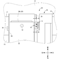
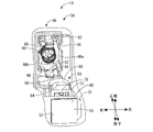
- FIG. 2 is an enlarged view of a main portion of the plan view of FIG. 1 (excluding the cover portion).
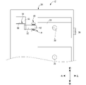
- FIG. 3 is an enlarged cross-sectional view of a main part taken along line III-III in FIG. 4 is a bottom view of the battery wiring module with the sensor unit shown in FIG. 2.
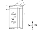
- FIG. 5 is an enlarged perspective view of a sensor unit arrangement area of the battery wiring module with a sensor unit shown in FIG. 1.
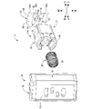
- FIG. 6 is an exploded perspective view of the sensor unit shown in FIG. 5.
- FIG. FIG. 7 is an exploded perspective view of the sensor unit shown in FIG. 6, viewed from the bottom side.
- FIG. 8 is a perspective enlarged view of the positioning protrusion of the upper housing shown in FIG. 3 as viewed from the bottom side.
- 9 is a bottom view of the upper housing shown in FIG. 8, and is an enlarged view of the positioning projection and the biasing member.
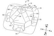
- FIG. 10 is an enlarged perspective view of the positioning protrusion of the sensor unit according to the second embodiment, and is a view corresponding to FIG. 8.
- FIG. 11 is a bottom view of the upper housing shown in FIG. 10, corresponding to FIG. 9. FIG.
- the sensor unit of the present disclosure is (1) a flexible strip-shaped conductive path structure including a thin plate-shaped conductor and an insulating film covering the conductor; a sensor element connected to the conductor; and a plate member disposed on the back surface of the conductive path structure and having one surface fixed to a portion facing the sensor element in the thickness direction of the conductive path structure. , wherein the other surface of the plate material is a contact surface with an object to be detected; In the sensor unit, the burr-forming portion of the flat metal plate is arranged inward in the bending direction.
- the metal plate fixed to the back surface of the conductive path structure has a shape in which a single metal flat plate is bent in the plate thickness direction to form a double layer, and burrs are formed on the metal flat plate.
- the part is arranged inward in the bending direction.
- a piece of metal plate may have burrs formed at the end of its cut end (side surface) in the shear direction.
- the present inventor paid attention to the fact that the burr formation site is limited to one end edge of the cut end (side surface) of the plate material, so that the burr formation site is inward in the bending direction.
- the structure of the present disclosure has been completed with the idea of adopting a plate member having a double-layered shape obtained by bending a flat metal plate in the plate thickness direction.
- a plate material By adopting such a plate material, even if the plate material has burrs, the burrs are arranged inward in the bending direction. Arrangement of burrs on the other surface side, which is the contact surface with the object to be detected, is avoided.
- the burr will come into contact with the conductive path structure and break the conductive path structure, and the burr will create a gap or rattle between the object to be detected and the plate material.
- the possibility that the detection accuracy of the sensor element is lowered due to the occurrence of such a phenomenon is suppressed.
- since it does not require the burr crushing process that is required for conventional plate materials it is possible to simplify the manufacturing process and reduce the manufacturing cost.
- the plate member has a first flat plate portion and a second flat plate portion that are superimposed on each other in the bending direction, and the overlapping surfaces of the first flat plate portion and the second flat plate portion are thermally conductive. It is preferably filled with resin.
- a thermally conductive resin is filled between overlapping surfaces of the first flat plate portion and the second flat plate portion that are mutually overlapped in the bending direction.
- an urging member that urges the plate member toward the object to be detected. Since the plate material is biased toward the object to be detected by the biasing member, the contact surface of the plate material can be stably held in contact with the object to be detected, thereby stabilizing the detection accuracy of the sensor element. and can be maintained.
- the urging member can be displaced toward the top wall side as the urging member is elastically deformed, and urged toward the plate member by an elastic restoring force of the urging member.
- the sensor unit further includes an upper housing that opens toward the surface of the conductive path structure, and a lower housing that is inserted into the upper housing from the opening side of the upper housing and displaceable in the axial direction of the upper housing.
- the lower housing has a sensor element accommodating portion that surrounds the sensor element and is fixed to the surface of the conductive path structure on the lower end side in the axial direction, the sensor element is protected from interference with other members. can do.
- an urging member can be arranged between the upper housing and the lower housing, and the elastic restoring force of the urging member can urge the lower housing toward the plate provided on the back surface of the conductive path structure.
- the contact surface of the plate can be stably pressed against the object to be detected by the elastic restoring force of the biasing member. As a result, it can be held in a pressed state. As a result, it is possible to provide a sensor unit capable of stably detecting the sensor element with a compact structure using the concentrically arranged upper housing and lower housing.
- the biasing member holding portion on the upper end side in the axial direction of the lower housing is configured to have a larger diameter than the sensor element housing portion on the lower end side in the axial direction.
- a stepped surface is provided between the upper housing and the sensor element accommodating portion, and the upper housing projects axially downward from the top wall portion facing the outer peripheral surface of the lower housing and is flexurally deformable radially outward.
- Each of the pair of elastic locking pieces has a pair of elastic locking pieces, each of which is provided with a locking projection protruding inward from the lower end of the pair of elastic locking pieces.
- the lower housing accommodated between the pieces can be displaced toward the top wall portion of the upper housing by elastic deformation of the biasing member, and is biased toward the plate member by the elastic restoring force of the biasing member. It is preferable that the displacement end on the plate member side is defined by locking the step surface of the lower housing to the locking projections of the pair of elastic locking pieces.
- the axially upper side (biasing member holding portion) of the lower housing By making the axially upper side (biasing member holding portion) of the lower housing larger in diameter than the axially lower side (sensor element accommodating portion), it is possible to form a stepped surface extending all the way around the lower housing. Further, a structure in which the lower housing is axially freely assembled to the upper housing can be easily constructed simply by projecting the pair of elastic locking pieces for holding the lower housing from the top wall portion of the upper housing. By making the radial dimension between the locking projections of the pair of elastic locking pieces smaller than the diameter dimension of the biasing member holding portion of the lower housing, the locking projections of the pair of elastic locking pieces are engaged with the step surface. A structure for stopping can be easily provided.
- the pair of elastic locking pieces is flexibly deformable radially outward, when the biasing member holding portion of the lower housing is inserted from the lower end side (locking projection side) of the pair of elastic locking pieces, the pair of elastic locking pieces The radially outward bending deformation of the locking piece allows the biasing member holding portion of the lower housing to be inserted into the ceiling wall portion side of the upper housing. After that, when the engaging projections in sliding contact with the outer peripheral surface of the lower housing pass over the stepped surfaces of the lower housing, the pair of elastic locking pieces elastically return radially inward, and the engaging projections are engaged with the stepped surfaces of the lower housing. stop.
- the displacement end of the lower housing toward the plate member is defined, and the lower housing is attached and held in a state that it can be displaced in the axial direction with respect to the upper housing.
- a battery wiring module with a sensor unit of the present disclosure is a battery wiring module with a sensor unit attached to a unit cell group in which a plurality of unit cells are arranged side by side, and is electrically connected to the unit cell group.
- the case includes a sensor unit arrangement area arranged on at least one of the cells that are objects to be detected, and the sensor unit is arranged in the sensor unit arrangement area 1.
- the battery wiring module attached to the unit cell group, which is the object to be detected is configured as a battery wiring module with a sensor unit provided with the sensor unit.
- the case of the battery wiring module includes a sensor unit placement area that is placed on the cells, which are objects to be detected. ing.
- the contact surface of the plate material of the sensor unit can be brought into contact with the unit cells, which are the objects to be detected, simply by assembling the sensor unit-equipped battery wiring module from above the unit cell group.
- the sensor unit is made of a flat metal plate that is double-folded so that the burr-forming portion is positioned inward in the direction of bending. In addition, it is possible to suppress breakage of the conductive path structure and deterioration of detection accuracy.
- the sensor unit arrangement area. and the upper housing is integrated with the case.
- the sensor unit arrangement area By arranging the sensor unit in the sensor unit arrangement area in a state in which the upper housing is oriented so as to open toward the unit cell, a stable plate material utilizing the biasing structure using the upper housing, the lower housing, and the biasing member is provided. Energization of single cells can be realized.
- the upper housing is integrated with the case, it is possible to improve the handleability of the wiring module with the sensor unit and reduce the number of parts. As a result, workability of assembling the wiring module with the sensor unit to the battery pack can be improved.
- FIG. 1 a sensor unit-equipped battery wiring module 12 including the sensor unit 10 according to the first embodiment of the present disclosure will be described with reference to FIGS. 1 to 9.
- FIG. The sensor unit-equipped battery wiring module 12 is attached to a cell group 16 in which a plurality of cells 14 are arranged side by side.
- the sensor unit-equipped battery wiring module 12 can be arranged in any direction, the vertical direction, the horizontal direction, and the front-rear direction are hereinafter based on the vertical direction, the left-right direction, and the front-rear direction shown in the drawing. explain. Further, with respect to a plurality of identical members, only some members are given reference numerals, and the reference numerals are omitted for other members.
- the unit cell group 16 includes a plurality of unit cells 14 arranged in a line.
- the cell group 16 including 12 cells 14 is illustrated in FIG. 1 , the number of cells 14 included in the cell group 16 is not limited to this.
- the unit cell group 16 includes a plurality of rows of the plurality of unit cells 14 arranged in a row.
- a plurality of cells 14 are arranged along a certain direction within the battery case 18 . More specifically, the unit cell 14 has an electrode forming surface on which a pair of positive electrode terminal 20a and negative electrode terminal 20b constituting the electrode terminal 20 are protruded. Hereinafter, the electrode formation surface may be referred to as the upper surface of the unit cell 14 .
- the plurality of single cells 14 are arranged in the battery case 18 with their electrode forming surfaces facing upward. Further, the plurality of unit cells 14 are arranged such that the positive electrode terminals 20a and the negative electrode terminals 20b of adjacent unit cells 14 are alternately positioned.
- a separator (not shown) made of resin or the like is arranged between the adjacent unit cells 14, and the plurality of unit cells 14 are arranged in a battery case 18 with a minute separator so that the side surfaces of the unit cells 14 are not in close contact with each other. Arranged with a gap. By forming a minute gap between adjacent unit cells 14, the minimum heat dissipation of each unit cell 14 can be ensured.
- a battery wiring module 12 with a sensor unit is attached to the cell group 16 in order to connect the cells 14 in parallel.
- the sensor unit-equipped battery wiring module 12 is attached to each terminal row 20c.
- a sensor unit-equipped battery wiring module 12 includes a plurality of cells 14 that electrically connect each adjacent cell 14 in a plurality of cells 14 arranged in a line. of busbars 22.
- the battery wiring module with sensor unit 12 includes an insulating case 26 having a busbar accommodation frame portion 24 that accommodates the plurality of busbars 22, a cover portion 28 that is attached to the case 26 and covers the plurality of busbars 22, and a sensor unit 10 .
- the bus bar 22 electrically connects the negative electrode terminal 20b of the cell 14 on the rearmost side and the positive electrode terminal 20a of the cell 14 on the frontmost side. Also, the bus bar 22 electrically connects the adjacent positive electrode terminal 20a and negative electrode terminal 20b. Thereby, a plurality of cells 14 are connected in series.
- Each bus bar 22 is a plate member made of a conductor such as copper, and has a through hole 30 in the center. By inserting a bolt (not shown) into each through-hole 30 and fastening the bolt, each bus bar 22 and the positive electrode terminal 20a and/or the negative electrode terminal 20b are fixed and electrically connected.
- the case 26 is, for example, an insulative synthetic resin plate member, and has a plurality of holes on both sides in the width direction (horizontal direction) into which the positive electrode terminals 20a and the negative electrode terminals 20b of the cell group 16 are respectively inserted. It has The case 26 is formed in a size corresponding to the surface on which the positive electrode terminal 20a or the negative electrode terminal 20b of the unit cell group 16 protrudes.
- the busbar accommodation frame portion 24 of the case 26 is a groove having a U-shaped cross section, and the busbar 22 is accommodated in the groove and placed on the bottom surface.
- a conductive path constructing passage 34 for wiring the conductive path constructing body 32 is provided in the width direction (horizontal direction) of the busbar housing frame portion 24 of the case 26 (see FIG. 4). ).
- the conductive path constituent wiring passage 34 has, for example, a tubular shape extending in the longitudinal direction, and the conductive path constituent 32 is arranged therein.
- the case 26 includes a sensor unit placement area A that is placed on one unit cell 14 (the frontmost unit cell 14 in this embodiment) that is an object to be detected (see FIGS. 2 and 4). ).
- the cover portion 28 is a flat plate-like member made of synthetic resin and having insulating properties.
- a plurality of engaging portions 36 extending downward are formed on the outer peripheral edge portion of the cover portion 28 . is fixedly attached to the case 26 (see FIG. 1).
- the sensor unit 10 is installed from above a single cell 14, which is an object to be detected.
- the sensor unit 10 includes a strip-shaped flexible conductive path structure 32 , a sensor element 40 connected to an end of the conductive path structure 32 , and a plate member 42 attached to the conductive path structure 32 . ing.
- the conductive path structure 32 consists of a pair of thin plate-shaped conductors 44, 44 made of copper foil, for example, and a strip-shaped insulating film 46 wider than the pair of conductors 44, 44. It is formed by covering. Therefore, the conductive path structure 32 has a highly flexible structure and a very space-saving structure as compared with the covered electric wire.
- a pair of connection portions 50, 50 are formed on a surface 48, which is an upper surface at the end portion of the conductive path structure 32, from which the pair of conductors 44, 44 are exposed.
- a pair of connecting portions 50 , 50 are formed by removing the insulating film 46 .
- Conductive path structure 32 is connected at the other end to a control unit (not shown) that controls unit cell group 16 .
- the sensor element 40 has a sensor main body 40a having a substantially rectangular shape.
- a pair of soldering portions 40b, 40b are provided at both ends of the sensor main body 40a.
- the pair of soldering portions 40b, 40b are electrically connected to the pair of conductors 44, 44 by being connected by soldering or the like to the pair of connection portions 50, 50 provided at the ends of the conductive path structure 32. It is Accordingly, a detection signal from the sensor element 40 arranged on the surface 48 of the conductive path structure 32 is input to the control unit through the pair of conductors 44, 44 of the conductive path structure 32.
- Any sensor such as a temperature sensor or a pressure sensor can be used as the sensor element 40 .
- the sensor element 40 is configured by a temperature sensor in this embodiment, it is not limited to this.
- the plate member 42 is formed in a flat plate shape with high flatness, as shown in FIG.
- the plate material 42 is arranged on the back surface 52 of the conductive path forming body 32, and the upper surface, which is one surface, is fixed by adhesion or crimping to a portion facing the sensor element 40 in the thickness direction of the conductive path forming body 32.
- the plate material 42 is made of a metal plate material having excellent heat conductivity, such as aluminum, an aluminum alloy, copper, or a copper alloy.
- the lower surface, which is the other surface of the plate member 42, is a contact surface with one unit cell 14, which is an object to be detected.
- the plate member 42 has a shape in which a single metal flat plate 54 is folded in the plate thickness direction to form a double layer, and has a first flat plate portion 54a and a second flat plate portion 54b that are overlapped with each other in the bending direction. is doing. Since the bent portion is slightly inferior in flatness, the portion other than the bent portion is fixed to the conductive path forming body 32 .
- a piece of metal flat plate 54 may have a burr formed at the end of its cut end (side surface) in the shear direction. That is, the burr formation site is limited to one end of the cut end (side surface) of the plate material. Therefore, the burrs are arranged so that the burrs are formed inward in the bending direction. Further, a thermally conductive resin 55 is filled between the overlapping surfaces of the first flat plate portion 54a and the second flat plate portion 54b.
- the thermally conductive resin 55 having higher thermal conductivity than the air layer. A decrease in heat transfer between the portions 54b can be suppressed.
- the overlapping surfaces of the first flat plate portion 54a and the second flat plate portion 54b may be brought into close contact with each other, and the heat conductive resin 55 is not necessarily provided.
- the thermally conductive resin 55 specifically, a silicone resin, a non-silicone acrylic resin, a ceramic resin, or the like can be used.
- a heat-dissipating gap filler heat-conducting grease, heat-conducting silicone rubber, etc. made of silicone-based resin
- the thermally conductive resin 55 may be formed in a sheet shape, have flexibility and elasticity, and be elastically deformable so that the thickness dimension changes according to the force applied in the vertical direction.
- the sensor unit 10 includes a bottomed tubular upper housing 56 that opens downward, a tubular lower housing 58 that opens both upward and downward, It has The sensor unit 10 is arranged in the sensor unit arrangement area A of the battery wiring module 12 with a sensor unit. The sensor unit 10 is oriented so that the upper housing 56 opens toward the unit cell 14 in the sensor unit arrangement area A, and the upper housing 56 is attached to the case 26 of the battery wiring module 12 with sensor unit. integrated and formed.
- the upper housing 56 is positioned on the surface 48 of the conductive path structure 32 and opens toward the surface 48, as shown in FIG.
- the upper housing 56 has a pair of elastic locking members that protrude downward in the axial direction from the top wall portion 60 so as to face the outer peripheral surface of the lower housing 58 and are capable of bending and deforming outward in the radial direction (horizontal direction in FIG. 3). It has strips 62,62. At the lower end of each pair of elastic locking pieces 62, locking projections 64 projecting inward and having square tubular shapes and substantially triangular cross-sections are provided. Further, as shown in FIGS.
- a peripheral wall portion 66 projecting from the periphery of the ceiling wall portion 60 of the upper housing 56 toward the surface 48 of the conductive path structure 32 pivots the biasing member 80. It surrounds the entire length of the direction (see FIGS. 3 and 7).
- peripheral wall facing surfaces 66a and 66b that face each other in the lateral direction are provided with a pair of guide ribs projecting toward the other side and extending in the axial direction (vertical direction). 68, 68 are spaced apart in the longitudinal direction.
- the other end portion in the axial direction of an urging member 80 projects in a tapered cylindrical shape from the central portion of the top wall portion 60 toward the lower housing 58, that is, downward in the axial direction. It has a positioning protrusion 70 inserted in (lower end).
- the positioning protrusion 70 has a pair of housing recesses 72, 72 which are open to the outer peripheral surface at the proximal end and are recessed inwardly.
- the accommodation recesses 72 are open on the outer peripheral surface of the positioning protrusion 70 and are provided at two locations spaced apart in the circumferential direction.
- the outer peripheral surface of the positioning projection 70 is provided with a guide recess 74 that positions an engaging projection 88 described later in the circumferential direction of the positioning projection 70 and extends in the axial direction of the positioning projection 70 toward the accommodation recess 72 . ing.
- Each of the guide recesses 74 is open on the outer peripheral surface of the positioning protrusion 70 and extends toward the base end. there is
- the housing recesses 72 are connected to the respective guide recesses 74 and open to the outer peripheral surface of the positioning protrusion 70 .
- the positioning protrusion 70 has two arc-shaped outer peripheral surfaces 76 that are protruding on the outer peripheral surface and are provided at two locations in the circumferential direction, and are adjacent to each other in the circumferential direction of the positioning protrusion 70 .
- the guide recesses 74 are connected in the circumferential direction via arcuate outer peripheral surfaces 76 arranged therebetween.
- Each guide recess 74 has a first guide surface 74a and a second guide surface 74b extending perpendicularly to each other with which a proximal portion 88a and a distal portion 88c of an engagement projection 88, which will be described later, abut, respectively.
- the first guide surface 74a is a flat surface extending in the vertical direction, which is the axial direction of the positioning protrusion 70, and in a direction orthogonal thereto.
- the second guide surface 74b extends perpendicularly to the first guide surface 74a toward the proximal end portion and has a projecting curved surface shape that is convex outward in the axial direction. That is, it spreads in the radial direction of the biasing member 80, which will be described later, and extends toward the base end.
- the lower housing 58 is mounted in the upper housing 56 so as to be displaceable in the axial direction of the upper housing 56, as shown in FIG. More specifically, the lower end in the axial direction of the lower housing 58 has a hollow cylindrical shape and surrounds the sensor element 40, and the lower end surface thereof is fixed to the surface 48 of the conductive path structure 32 using an adhesive or the like. It constitutes a sensor element accommodating portion 77 .
- An inner wall of the sensor element accommodating portion 77 is provided with a pair of retaining projections 78, 78 protruding inward (see FIG. 7).
- a sealing material 79 for protecting the sensor element 40 from water, dust, etc.
- the upper end of the lower housing 58 in the axial direction constitutes a support portion 82 as a biasing member holding portion that holds a biasing member 80 that is axially stretchable between the surfaces facing the top wall portion 60 of the upper housing 56 . ing. That is, the support portion 82 supports one axial end portion of the biasing member 80 .
- the biasing member 80 is a metal coil spring formed by spirally winding a metal wire such as SUS.
- the lower housing 58 can be displaced toward the positioning protrusion 70 of the top wall portion 60 by the elastic deformation of the biasing member 80 contracting in the axial direction. It is adapted to be biased toward the plate member 42 side, that is, toward the unit cell 14 . That is, the biasing member 80 biases the lower housing 58 toward the cell 14, which is the object to be detected.
- the lower housing 58 is assembled to the upper housing 56 with the biasing member 80 interposed therebetween in the axial direction of the biasing member 80 .
- a support portion 82 on the upper end side in the axial direction of the lower housing 58 is configured to have a larger diameter than the sensor element housing portion 77 on the lower end side in the axial direction. is provided.
- the supporting portion 82 has a portion of the peripheral wall 86 that faces in the left-right direction and is notched over the entire length in the vertical direction.
- the upper end portion which is the other end portion of the biasing member 80, protrudes the ends of the strands of the biasing member 80 to the inner peripheral side of the biasing member 80 to bias.
- An engaging protrusion 88 is provided axially inwardly of the member 80 so as to be flexibly deformable.
- the engaging protrusion 88 includes a proximal portion 88a extending toward the inner peripheral side of the biasing member 80, a curved portion 88b connected to the proximal portion 88a, and a curved portion 88b connected to the curved portion 88b to bias the curved portion 88b.
- the proximal portion 88a and the distal portion 88c of the engaging protrusion 88 extend in the radial directions of the biasing member 80 perpendicular to each other, and the central angle ⁇ on the inner peripheral surface of the biasing member 80 is 90°. It protrudes in an L-shape in a plan view from an arcuate portion 90 described below.
- ⁇ Method for assembling battery wiring module 12 with sensor unit An outline of a method for assembling the battery wiring module 12 with a sensor unit according to the first embodiment of the present disclosure will be described.
- the sensor element 40 is soldered to the pair of connection portions 50 , 50 provided on the surface 48 of the end portion of the conductive path structure 32 .
- a plate member 42 is fixed to a portion of the rear surface 52 of one end of the conductive path structure 32 facing the sensor element 40 .
- the lower housing 58 is fixed around the sensor element 40 on the end surface 48 of the conductive path structure 32, and the sealing material 79 is injected into the sensor element accommodating portion 77 and hardened.
- the conductive path constructing body 32 is placed in the conductive path constructing path 34 provided on the surface side of the case 26 .
- the other end of the conductive path constructing body 32 is connected to a connector 94, and the connector 94 is attached to the rear end of the conductive path constructing passage 34.
- the biasing member 80 is moved to the positioning protrusion 70 side. push into.
- the proximal portion 88a and the distal portion 88c of the engaging protrusion 88 of the biasing member 80 are engaged with the first guide surface 74a and the second guide surface 74b of the guide recess 74 of the positioning protrusion 70, respectively.
- the engagement protrusion 88 and the biasing member 80 are aligned in the circumferential direction of the positioning protrusion 70 .
- the engaging projection 88 of the biasing member 80 is flexurally deformed inward in the axial direction of the biasing member 80 to allow the insertion of the biasing member 80 into the positioning projection 70 .
- the engaging protrusion 88 of the biasing member 80 is guided by the guide recess 74 and reaches the housing recess 72 .
- the engaging protrusion 88 is elastically restored and received and locked in the receiving recess 72 , and the biasing member 80 is held by the positioning protrusion 70 .
- one end of the conductive path structure 32 is moved to the back side of the case 26 through the opening hole 92 (see FIG. 4) and the slit 96 provided in the case 26 .
- the support portion 82 of the lower housing 58 is inserted between the pair of elastic locking pieces 62 , 62 of the upper housing 56 opening on the surface of the case 26 .
- the pair of elastic locking pieces 62, 62 are elastically deformed radially outward to allow the insertion of the support portion 82. As shown in FIG.
- the pair of elastic locking pieces 62 , 62 are elastically restored, and the step surface 84 of the lower housing 58 is locked to the locking projections 64 of the pair of elastic locking pieces 62 , 62 . That is, the displacement end on the plate member 42 side is defined by the stepped surface 84 of the lower housing 58 engaging the locking projections 64 of the pair of elastic locking pieces 62 , 62 .
- the case 26 configured in this manner is assembled to the cell group 16 .
- the lower housing 58 is pushed upward by the plate member 42 coming into contact with the surface of the cell 14, and the biasing member 80 biases the lower housing 58 downward.
- the sensor unit 10 in the sensor unit arrangement area A, the sensor unit 10 is arranged in such a manner that the plate member 42 can come into contact with the cell 14 , and is pressed against the cell 14 by the biasing member 80 .
- the sensor unit 10 includes a biasing member 80 that biases the plate member 42 toward the unit cell 14, which is an object to be detected.
- the busbar 22 and the cover portion 28 are attached to the case 26 to complete the battery wiring module 12 with the sensor unit.
- the metal plate member 42 fixed to the back surface 52 of the conductive path structure 32 is formed by bending one metal flat plate 54 in the plate thickness direction. It has a weighted shape.
- the burr forming portion is arranged inward in the bending direction. That is, the present inventors paid attention to the fact that the burr formation site is limited to one end of the cut end (side surface) of one metal flat plate 54, and the burr formation site is inward in the bending direction.
- the plate member 42 having a shape in which a single metal flat plate 54 is bent in the plate thickness direction and doubled is adopted.
- the burrs are arranged inward in the bending direction. Therefore, burrs are placed on one side of the plate member 42 fixed to the back surface 52 of the conductive path structure 32 and on the other side of the plate member 42 that is the contact surface with the unit cell 14 that is the object to be detected. is avoided. Therefore, even when the metal plate member 42 is employed, the burr may come into contact with the conductive path forming body 32 to break the conductive path forming body 32, and the burr may cause the unit cell 14 to be detected. A decrease in the detection accuracy of the sensor element 40 due to a gap or backlash between the plate member 42 and the sensor element 40 is suppressed.
- the sensor element 40 is a temperature sensor, the heat collection effect of the plate member 42 can be used to stabilize the detection of the sensor element 40 and the like.
- the sensor unit 10 includes an upper housing 56 that opens toward the surface 48 of the conductive path structure 32, and is inserted into the upper housing 56 from the opening side of the upper housing 56 so as to be displaceable in the axial direction of the upper housing 56.
- a lower housing 58 is further provided.
- the lower end of the lower housing 58 in the axial direction serves as a sensor element accommodating portion 77 which surrounds the sensor element 40 and is fixed to the surface 48 of the conductive path structure 32. It can be protected from interference and the like.
- the biasing member 80 By arranging the biasing member 80 between the upper housing 56 and the lower housing 58 , the lower housing 58 can be biased toward the plate member 42 provided on the rear surface 52 of the conductive path structure 32 .
- the plate member 42 can be stably attached to the unit cell 14 by the elastic restoring force of the biasing member 80 on the contact surface with the unit cell 14. can be held in a pressed state.
- the sensor unit 10 capable of stably detecting the sensor element 40 with a compact structure using the coaxially arranged upper housing 56 and lower housing 58 .
- the step surface 84 of the lower housing 58 can be configured over the entire circumference. Further, simply by protruding the pair of elastic locking pieces 62, 62 for holding the lower housing 58 from the ceiling wall portion 60 of the upper housing 56, a structure for freely assembling the lower housing 58 to the upper housing 56 in the axial direction can be easily constructed. can. More specifically, the radial dimension between the locking projections 64 of the pair of elastic locking pieces 62 , 62 is smaller than the radial dimension of the support portion 82 of the lower housing 58 .
- the displacement end of the lower housing 58 toward the plate member 42 side is defined, and the lower housing 58 is mounted and held in a state displaceable in the axial direction toward the ceiling wall portion 60 of the upper housing 56 .
- a battery wiring module attached to the unit cell group 16, which is an object to be detected is configured as a sensor unit-equipped battery wiring module 12 having the sensor unit 10.
- the case 26 of the sensor unit-equipped battery wiring module 12 includes a sensor unit placement area A that is placed on the unit cell 14, which is an object to be detected.
- the sensor unit 10 is arranged such that the plate member 42 of the sensor unit 10 can come into contact with the cell 14 .
- the contact surface of the plate member 42 of the sensor unit 10 can be brought into contact with the unit cell 14, which is the object to be detected, simply by assembling the sensor unit-equipped battery wiring module 12 from above the unit cell group 16.
- the plate member 42 of the sensor unit 10 is formed by bending the flat metal plate 54 in two and arranging the burr forming portion inward in the bending direction. Therefore, it is possible to suppress the breakage of the conductive path forming body 32 and the deterioration of the detection accuracy of the sensor element 40 while simplifying the manufacturing process and suppressing the manufacturing cost.
- the upper housing 56 is arranged in the sensor unit arrangement area A in a state of being oriented so as to open toward the cell 14 .
- the biasing structure using the upper housing 56 , the lower housing 58 , and the biasing member 80 can be used to achieve stable biasing of the plate member 42 to the single cell 14 .
- the upper housing 56 is integrated with the case 26, the handling of the battery wiring module 12 with sensor unit is improved and the number of parts is reduced. Therefore, the workability of assembling the sensor unit-equipped battery wiring module 12 to the cell group 16 can be improved.
- the engaging protrusion 88 of the biasing member 80 protrudes in an L shape in a plan view from the arc-shaped portion 90 having a central angle ⁇ of 90° or less.
- the guide recesses 74 are evenly arranged at two locations spaced apart from each other in the circumferential direction, the present invention is not limited to this.
- the positioning projection 98 of the second embodiment of the present disclosure shown in FIGS. and may protrude in a V-shape in plan view from an arcuate portion 90 having a central angle of 90° or less on the inner peripheral surface of the biasing member 80 .
- the engaging projection 101 also has a proximal portion 101a extending toward the inner peripheral side of the biasing member 80, a curved portion 101b connected to the proximal portion 101a, and a curved portion connected to the curved portion 101b. and a distal portion 101c extending toward the outer peripheral side of the biasing member 80 from the portion 101b.
- a flat guide surface 100 extending gradually widening toward the base end portion is formed on the outer peripheral surface of the positioning protrusion 98 so as to be spaced apart from each other in the circumferential direction. are evenly distributed in four locations.
- the proximal end of the positioning protrusion 98 is provided with four locking recesses 102 that open in contact with the guide surface 100 at four locations in the circumferential direction corresponding to the guide surface 100 . Furthermore, the positioning protrusion 98 has four circular arc-shaped outer peripheral surfaces 104 which are provided at four locations in the circumferential direction and which are protruding on the outer peripheral surface. Adjacent guide surfaces 100 are connected via arc-shaped outer peripheral surfaces 104 arranged therebetween.
- the guide surfaces 100 can be provided at four locations spaced apart in the circumferential direction of the positioning protrusion 98, the biasing member 80 can be assembled to the positioning protrusion 98 in many directions, improving assembly workability. can be achieved.
- Circular outer peripheral surfaces 104 are arranged between the four flat guide surfaces 100 provided on the positioning protrusion 98 in the circumferential direction. Therefore, even when the circumferential position of the engaging projection 101 is deviated from the guide surface, the engaging projection 88 in contact with the arc-shaped outer peripheral surface 104 is guided toward the guide surface 100, and the engaging projection 88 is engaged.
- the protrusion 101 can be advantageously guided into the correct circumferential position and securely locked into the locking recess 102 .
- a metal coil spring formed by spirally winding a metal wire rod as the biasing member 80 has been described as an example, but the present invention is not limited to this.
- the biasing member 80 any member can be adopted as long as it can bias the plate member 42 toward the object to be detected. good.
- the biasing member 80 may be like the biasing member of US Pat.
- the biasing member 80 may be omitted.
- the plate member 42 of the sensor unit may be pressed against the object to be detected.
- sensor unit (embodiment 1) 12 Battery wiring module with sensor unit 14 Cell (object to be detected) 16 Cell Group 18 Battery Case 20 Electrode Terminal 20a Positive Electrode Terminal 20b Negative Electrode Terminal 20c Terminal Row 22 Busbar 24 Busbar Accommodating Frame 26 Case 28 Cover 30 Penetration Hole 32 Conductive Path Constituent 34 Conductive Constructive Structure Wiring Passage 36 Engaging portion 38 Engaged portion 40 Sensor element 40a Sensor body 40b Soldering portion 42 Plate material 44 Conductor 46 Insulating film 48 Front surface 50 Connection portion 52 Back surface 54 Metal flat plate 54a First flat plate portion 54b Second flat plate portion 55 Heat Conductive resin 56 Upper housing 58 Lower housing 60 Top wall 62 Elastic locking piece 64 Locking projection 66 Peripheral wall 66a Peripheral wall facing surface 66b Peripheral wall facing surface 68 Guide projection 70 Positioning projection 72 Accommodating recess 74 Guide recess 74a No.
Landscapes
- Chemical & Material Sciences (AREA)
- Chemical Kinetics & Catalysis (AREA)
- Electrochemistry (AREA)
- General Chemical & Material Sciences (AREA)
- Engineering & Computer Science (AREA)
- Manufacturing & Machinery (AREA)
- Physics & Mathematics (AREA)
- General Physics & Mathematics (AREA)
- Microelectronics & Electronic Packaging (AREA)
- General Engineering & Computer Science (AREA)
- Inorganic Chemistry (AREA)
- Mechanical Engineering (AREA)
- Connection Of Batteries Or Terminals (AREA)
- Battery Mounting, Suspending (AREA)
- Springs (AREA)
Abstract
Description
最初に、本開示の実施態様を列記して説明する。
本開示のセンサユニットは、
(1)薄板状の導体と、前記導体を被覆する絶縁性フィルムと、を含んで構成された可撓性を有する帯状の導電路構成体と、前記導電路構成体の表面に配置されて、前記導体に接続されたセンサ素子と、前記導電路構成体の裏面に配置されて、前記導電路構成体の厚さ方向で前記センサ素子と対向する部位に、一方の面が固着された板材と、を備え、前記板材の他方の面は、被検出体への接触面であり、前記板材が、一枚の金属平板を板厚方向に折り曲げて二重にした形状を有しており、前記金属平板のバリ形成部位が、折り曲げ方向の内方に配置されている、センサユニットである。
本開示のセンサユニットおよびセンサユニット付電池配線モジュールの具体例を、以下に図面を参照しつつ説明する。なお、本開示は、これらの例示に限定されるものではなく、特許請求の範囲によって示され、特許請求の範囲と均等の意味および範囲内でのすべての変更が含まれることが意図される。
以下、本開示の実施形態1のセンサユニット10を備えたセンサユニット付電池配線モジュール12について、図1から図9を用いて説明する。センサユニット付電池配線モジュール12は、複数の単電池14が並べて配置された単電池群16に装着される。なお、センサユニット付電池配線モジュール12は、任意の向きで配置することができるが、以下では、上下方向,左右方向,前後方向を、図中に示す上下方向,左右方向および前後方向を基準として説明する。また、複数の同一部材については、一部の部材にのみ符号を付し、他の部材については符号を省略する場合がある。
単電池群16は、一列に配列された複数の単電池14を備える。なお、図1においては、12個の単電池14を備える単電池群16が例示されているが、単電池群16が備える単電池14の個数はこれに限らない。また、単電池群16は、一列に配列された複数の単電池14を複数列分備える場合もある。
図1に示すように、本開示の実施形態1のセンサユニット付電池配線モジュール12は、一列に並べられた複数の単電池14における1個毎に隣接する単電池14を電気的に接続する複数のバスバー22を有している。また、センサユニット付電池配線モジュール12は、複数のバスバー22を収容するバスバー用収容枠部24を有する絶縁性のケース26と、ケース26に装着されて複数のバスバー22を覆うカバー部28と、センサユニット10と、を有している。
バスバー22は、最も後方側の単電池14の負電極端子20bと最も前方側の単電池14の正電極端子20aを電気的に接続する。また、バスバー22は、隣接する正電極端子20aと負電極端子20bを電気的に接続する。これにより、複数の単電池14が直列に接続されている。
ケース26は、例えば、絶縁性を有する合成樹脂製の板部材であり、幅方向(左右方向)の両側に単電池群16の正電極端子20aと負電極端子20bがそれぞれ挿入される複数の穴を備えている。ケース26は、単電池群16の正電極端子20aあるいは負電極端子20bが突設された面に対応する大きさに形成されている。ケース26のバスバー用収容枠部24は、断面がU字状の溝であり、バスバー22が溝に収容され底面に載置されている。
カバー部28は、絶縁性を有する合成樹脂製の平板状の部材である。カバー部28の外周縁部には、下方に向かって延びる複数の係合部36が形成されており、対応するケース26側に設けられた被係合部38と係合することによりカバー部28がケース26に対して固定的に取り付けられている(図1参照)。
センサユニット10は、被検出体である1つの単電池14に対して上方から設置するものである。センサユニット10は、帯状の可撓性を有する導電路構成体32と、導電路構成体32の端部に接続されるセンサ素子40と、導電路構成体32に取り付けられる板材42と、を備えている。
導電路構成体32は、図3および図6に示すように、例えば銅箔からなる一対の薄板状の導体44,44を、一対の導体44,44よりも幅広な帯状の絶縁性フィルム46で被覆して形成されている。したがって、導電路構成体32は、被覆電線に比べて柔軟性が高く非常に省スペースな構成となっている。導電路構成体32の端部における上面である表面48には、一対の導体44,44が露出した一対の接続部50,50が形成されている。一対の接続部50,50は、絶縁性フィルム46を除去することにより形成されている。導電路構成体32は、他方の端部において単電池群16を制御する図示しない制御ユニットに接続されている。
センサ素子40は、図3および図6に示すように、略方形状をなすセンサ本体40aを有している。センサ本体40aの両端部には、一対の半田付け部40b,40bが設けられている。一対の半田付け部40b,40bは、導電路構成体32の端部に設けられた一対の接続部50,50に半田などで接続されることにより、一対の導体44,44に電気的に接続されている。したがって、導電路構成体32の表面48上に配置されたセンサ素子40からの検出信号が導電路構成体32の一対の導体44,44を通じて制御ユニットに入力されるようになっている。なお、センサ素子40としては、温度センサや圧力センサ等の任意のセンサが採用可能である。本実施形態では、センサ素子40は温度センサによって構成されているが、これに限定されない。
板材42は、図3に示すように、平坦度の高い平板状に形成されている。板材42は、導電路構成体32の裏面52に配置されており、導電路構成体32の厚さ方向でセンサ素子40と対向する部位に一方の面である上面が接着や圧着により固着されている。板材42は、アルミニウム、アルミニウム合金あるいは銅、銅合金などの伝熱性に優れた金属板材により構成されている。板材42の他方の面である下面は、被検出体である1つの単電池14への接触面である。板材42は、一枚の金属平板54を板厚方向に折り曲げて二重にした形状を有しており、折り曲げ方向で相互に重ね合された第1平板部54aと第2平板部54bを有している。折り曲げ部分は平坦度がやや劣ることから、折り曲げ部分を除く部分で導電路構成体32と固着されている。一枚の金属平板54は、その切り口(側面)のせん断方向の終端にバリが形成される場合がある。すなわち、バリの形成部位は、板材の切り口(側面)の一方の端部に限定されている。そこで、バリ形成部位が折り曲げ方向の内方となるように配置したのである。さらに、第1平板部54aと第2平板部54bの重ね合せ面間を熱伝導性樹脂55で充填している。
アッパハウジング56は、図3に示すように、導電路構成体32の表面48上に配置されており、表面48に向かって開口している。また、アッパハウジング56は、ロアハウジング58の外周面に対向して天壁部60から軸方向下方に突出して径方向(図3中、左右方向)外方に撓み変形可能な一対の弾性係止片62,62を有している。各一対の弾性係止片62の下端部には、内側に向かって突出する角筒状の略三角断面形状の係止突起64が設けられている。さらに、図3,図5,図7に示すように、アッパハウジング56の天壁部60の周囲から導電路構成体32の表面48に向かって突出する周壁部66が、付勢部材80を軸方向の全長に亘って囲っている(図3,図7参照)。加えて、周壁部66において、短手方向(図7中、左右方向)に対向する周壁対向面66a,66bには、相手側に向かって突出し軸方向(上下方向)に延びる一対のガイド突条68,68が前後方向に離隔して設けられている。
位置決め突部70は、図3および図8,図9に示すように、基端部において外周面に開口して内周側に凹んでいる一対の収容凹所72,72を有している。収容凹所72は位置決め突部70の外周面に開口しており、周方向に離隔した2か所に設けられている。位置決め突部70の外周面には、後述する係合突起88を位置決め突部70の周方向に位置決めして収容凹所72に向かって位置決め突部70の軸方向に延びる案内凹部74が設けられている。各案内凹部74は、位置決め突部70の外周面に開口して基端部に向かって延びており、位置決め突部70の外周面において周方向で相互に離隔した2か所に均等配置されている。収容凹所72は、それぞれの案内凹部74に連接して位置決め突部70の外周面に開口している。位置決め突部70は、周方向の2か所に相互に離隔して設けられた外周面に凸となる2つの円弧状外周面76を有しており、位置決め突部70の周方向で隣接する案内凹部74間が、それらの間に配置された各円弧状外周面76を介して周方向で連接されている。各案内凹部74は、後述する係合突起88の近位部88aと遠位部88cがそれぞれ当接する相互に直交して広がる第1の案内面74aと第2の案内面74bを有している。第1の案内面74aは、位置決め突部70の軸方向である上下方向とそれに直交する方向に延びる平坦面とされている。第2の案内面74bは、第1の案内面74aに直交して基端部に向かって、軸直方向外方に向かって凸となる突状湾曲面形状を有して延びている。すなわち、後述する付勢部材80の半径方向で広がり且つ基端部に向かって延びている。
ロアハウジング58は、図3に示すように、アッパハウジング56の軸方向に変位可能な状態でアッパハウジング56内に装着されている。より詳細には、ロアハウジング58の軸方向下端側は、中空筒状でセンサ素子40の周囲を囲って、その下端面が導電路構成体32の表面48に接着剤等を用いて固着されてセンサ素子収容部77を構成している。センサ素子収容部77の内壁には、内側に向かって突出する一対の抜止突起78,78が設けられている(図7参照)。センサ素子収容部77内には、センサ素子40を水や塵埃などから保護するための封止材79が注入され、封止材79が硬化することで、封止材79は、センサ素子40を覆いつつ、一対の抜止突起78によって抜け止めされるようになっている。ロアハウジング58の軸方向上端側は、アッパハウジング56の天壁部60との対向面間で軸方向に伸縮自在な付勢部材80を保持する付勢部材保持部としての支持部82を構成している。すなわち、支持部82は、付勢部材80の軸方向の一端部を支持している。付勢部材80は、SUSなどの金属線材を螺旋状に巻回した金属製のコイルばねとされている。この結果、ロアハウジング58は、付勢部材80の軸方向に収縮する弾性変形に伴い天壁部60の位置決め突部70に向かって変位可能となっており、付勢部材80の弾性復帰力により板材42側すなわち単電池14に向かって付勢されるようになっている。すなわち、付勢部材80は、被検出体である単電池14に向けてロアハウジング58を付勢している。また、ロアハウジング58は、付勢部材80の軸方向で、付勢部材80を間に挟んでアッパハウジング56に組み付けられている。
付勢部材80の他端部である上端部は、図3,図6および図9に示すように、付勢部材80の素線の端末を付勢部材80の内周側に突出して付勢部材80の軸方向内方に撓み変形可能に構成した係合突起88を有している。係合突起88は、付勢部材80の内周側に向かって延びる近位部88aと、近位部88aに連接する湾曲部88bと、湾曲部88bに連接して湾曲部88bよりも付勢部材80の外周側に向かって延びる遠位部88cとを有している。係合突起88の近位部88aと遠位部88cが、相互に直交する付勢部材80の半径方向にそれぞれ延びており、付勢部材80の内周面において、中心角:αが90°以下の円弧状部90から平面視でL字形状に突出している。
本開示の実施形態1のセンサユニット付電池配線モジュール12の組立方法の概略について説明する。はじめに、導電路構成体32の端部の表面48に設けられた一対の接続部50,50にセンサ素子40を半田付けする。その後、導電路構成体32の一方の端部の裏面52におけるセンサ素子40と対向する部位に板材42を固着する。その後、導電路構成体32の端部の表面48のセンサ素子40の周囲にロアハウジング58を固着し、センサ素子収容部77内に封止材79を注入し硬化する。続いて、ケース26の表面側に設けられた導電路構成体配索用通路34に導電路構成体32を配置する。導電路構成体32の他方の端部をコネクタ94に接続し、コネクタ94を導電路構成体配索用通路34の後端部に取り付ける。次に、センサユニット配置領域Aに設けられたアッパハウジング56の位置決め突部70の軸に対して付勢部材80の軸を合わせるように位置決めした状態で、付勢部材80を位置決め突部70側に押し込む。この際、付勢部材80の係合突起88の近位部88aと遠位部88cがそれぞれ位置決め突部70の案内凹部74の第1の案内面74aと第2の案内面74bに係合することで、位置決め突部70の周方向で係合突起88や付勢部材80が位置合わせされる。これにより、付勢部材80の係合突起88が付勢部材80の軸方向内方へ撓み変形されて、位置決め突部70に対する付勢部材80の内挿が許容される。そして、付勢部材80の係合突起88が案内凹部74に案内されて収容凹所72に到達する。この結果、係合突起88が弾性復帰して収容凹所72に収容されて係止され、付勢部材80が位置決め突部70に保持される。
本明細書に記載された技術は上記記述および図面によって説明した実施形態に限定されるものではなく、例えば次のような実施形態も本明細書に記載された技術の技術的範囲に含まれる。
12 センサユニット付電池配線モジュール
14 単電池(被検出体)
16 単電池群
18 電池ケース
20 電極端子
20a 正電極端子
20b 負電極端子
20c 端子列
22 バスバー
24 バスバー用収容枠部
26 ケース
28 カバー部
30 貫通孔
32 導電路構成体
34 導電路構成体配索用通路
36 係合部
38 被係合部
40 センサ素子
40a センサ本体
40b 半田付け部
42 板材
44 導体
46 絶縁性フィルム
48 表面
50 接続部
52 裏面
54 金属平板
54a 第1平板部
54b 第2平板部
55 熱伝導性樹脂
56 アッパハウジング
58 ロアハウジング
60 天壁部
62 弾性係止片
64 係止突起
66 周壁部
66a 周壁対向面
66b 周壁対向面
68 ガイド突条
70 位置決め突部
72 収容凹所
74 案内凹部
74a 第1の案内面
74b 第2の案内面
76 円弧状外周面
77 センサ素子収容部
78 抜止突起
79 封止材
80 付勢部材
82 支持部(付勢部材保持部)
84 段差面
86 周壁
88 係合突起
88a 近位部
88b 湾曲部
88c 遠位部
90 円弧状部
92 開口穴
94 コネクタ
96 スリット
98 位置決め突部
100 案内面
101 係合突起
101a 近位部
101b 湾曲部
101c 遠位部
102 係止凹所
104 円弧状外周面
A センサユニット配置領域
Claims (7)
- 薄板状の導体と、前記導体を被覆する絶縁性フィルムと、を含んで構成された可撓性を有する帯状の導電路構成体と、
前記導電路構成体の表面に配置されて、前記導体に接続されたセンサ素子と、
前記導電路構成体の裏面に配置されて、前記導電路構成体の厚さ方向で前記センサ素子と対向する部位に、一方の面が固着された板材と、を備え、
前記板材の他方の面は、被検出体への接触面であり、
前記板材が、一枚の金属平板を板厚方向に折り曲げて二重にした形状を有しており、前記金属平板のバリ形成部位が、折り曲げ方向の内方に配置されている、
センサユニット。 - 前記板材は、前記折り曲げ方向で相互に重ね合された第1平板部と第2平板部を有し、前記第1平板部と前記第2平板部の重ね合せ面間が熱伝導性樹脂で充填されている、請求項1に記載のセンサユニット。
- 前記板材を前記被検出体に向かって付勢する付勢部材を備える、請求項1または請求項2に記載のセンサユニット。
- 前記導電路構成体の前記表面上に配置されて、前記表面に向かって開口する有底筒状のアッパハウジングと、
前記アッパハウジングの軸方向に変位可能な状態で前記アッパハウジング内に装着される筒状のロアハウジングと、を備え、
前記ロアハウジングの軸方向下端側は、前記センサ素子の周囲を囲って前記導電路構成体の前記表面に固着されてセンサ素子収容部を構成し、前記ロアハウジングの軸方向上端側は、前記アッパハウジングの天壁部との対向面間で軸方向に伸縮自在な前記付勢部材を保持する付勢部材保持部を構成し、
前記ロアハウジングは、前記付勢部材の弾性変形に伴い前記天壁部側に変位可能で、前記付勢部材の弾性復帰力により前記板材側に付勢される、請求項3に記載のセンサユニット。 - 前記ロアハウジングの前記軸方向上端側の前記付勢部材保持部は、前記軸方向下端側の前記センサ素子収容部よりも大径に構成されており、前記付勢部材保持部と前記センサ素子収容部との間に段差面が設けられており、
前記アッパハウジングは、前記ロアハウジングの外周面に対向して前記天壁部から軸方向下方に突出して径方向外方に撓み変形可能な一対の弾性係止片を有し、各前記一対の弾性係止片の下端部には、内側に向かって突出する係止突起が設けられており、
前記アッパハウジングの前記一対の弾性係止片の間に収容された前記ロアハウジングは、前記付勢部材の弾性変形により前記アッパハウジングの前記天壁部に向かって変位可能であり、前記付勢部材の弾性復帰力により前記板材側に付勢され、前記板材側の変位端が、前記ロアハウジングの前記段差面が、前記一対の弾性係止片の前記係止突起に係止することにより規定されている、請求項4に記載のセンサユニット。 - 複数の単電池が並べて配置された単電池群に装着されるセンサユニット付電池配線モジュールであって、
前記単電池群に電気的に接続された複数のバスバーと、
前記複数のバスバーを収容する絶縁性のケースと、
前記ケースに装着されて前記複数のバスバーを覆うカバー部と、を有し、
センサユニットとして、請求項1~5のいずれか1項に記載のセンサユニットを用い、
前記ケースは、被検出体である少なくとも1つの前記単電池上に配置されるセンサユニット配置領域を含み、
前記センサユニット配置領域において、前記センサユニットが、前記板材が前記単電池に接触可能な状態で配置されている、
センサユニット付電池配線モジュール。 - 前記センサユニットとして、請求項4または請求項5に記載のセンサユニットを用い、
前記アッパハウジングが前記単電池に向かって開口するように配向された状態で、前記センサユニット配置領域に配置され、前記アッパハウジングが前記ケースに一体化されている、請求項6に記載のセンサユニット付電池配線モジュール。
Priority Applications (3)
| Application Number | Priority Date | Filing Date | Title |
|---|---|---|---|
| US18/559,373 US20240274904A1 (en) | 2021-05-26 | 2022-02-11 | Sensor unit and sensor unit-equipped battery wiring module |
| JP2023523984A JP7486028B2 (ja) | 2021-05-26 | 2022-02-11 | センサユニットおよびセンサユニット付電池配線モジュール |
| CN202280033871.6A CN117280182A (zh) | 2021-05-26 | 2022-02-11 | 传感器单元及带传感器单元的电池布线模块 |
Applications Claiming Priority (2)
| Application Number | Priority Date | Filing Date | Title |
|---|---|---|---|
| JP2021-088579 | 2021-05-26 | ||
| JP2021088579 | 2021-05-26 |
Publications (1)
| Publication Number | Publication Date |
|---|---|
| WO2022249574A1 true WO2022249574A1 (ja) | 2022-12-01 |
Family
ID=84229794
Family Applications (1)
| Application Number | Title | Priority Date | Filing Date |
|---|---|---|---|
| PCT/JP2022/005524 Ceased WO2022249574A1 (ja) | 2021-05-26 | 2022-02-11 | センサユニットおよびセンサユニット付電池配線モジュール |
Country Status (4)
| Country | Link |
|---|---|
| US (1) | US20240274904A1 (ja) |
| JP (1) | JP7486028B2 (ja) |
| CN (1) | CN117280182A (ja) |
| WO (1) | WO2022249574A1 (ja) |
Families Citing this family (1)
| Publication number | Priority date | Publication date | Assignee | Title |
|---|---|---|---|---|
| CN120709634B (zh) * | 2025-08-26 | 2026-01-06 | 宁德时代新能源科技股份有限公司 | 电池装置和用电设备 |
Citations (4)
| Publication number | Priority date | Publication date | Assignee | Title |
|---|---|---|---|---|
| WO2012137289A1 (ja) * | 2011-04-04 | 2012-10-11 | 日立ビークルエナジー株式会社 | 蓄電モジュール |
| JP2014093163A (ja) * | 2012-11-01 | 2014-05-19 | Yazaki Corp | バスバモジュールの電線配索構造 |
| WO2015122496A1 (ja) * | 2014-02-14 | 2015-08-20 | 矢崎総業株式会社 | バスバモジュール |
| JP2019074327A (ja) * | 2017-10-12 | 2019-05-16 | 株式会社オートネットワーク技術研究所 | センサユニットおよび蓄電モジュール |
-
2022
- 2022-02-11 US US18/559,373 patent/US20240274904A1/en active Pending
- 2022-02-11 CN CN202280033871.6A patent/CN117280182A/zh active Pending
- 2022-02-11 WO PCT/JP2022/005524 patent/WO2022249574A1/ja not_active Ceased
- 2022-02-11 JP JP2023523984A patent/JP7486028B2/ja active Active
Patent Citations (4)
| Publication number | Priority date | Publication date | Assignee | Title |
|---|---|---|---|---|
| WO2012137289A1 (ja) * | 2011-04-04 | 2012-10-11 | 日立ビークルエナジー株式会社 | 蓄電モジュール |
| JP2014093163A (ja) * | 2012-11-01 | 2014-05-19 | Yazaki Corp | バスバモジュールの電線配索構造 |
| WO2015122496A1 (ja) * | 2014-02-14 | 2015-08-20 | 矢崎総業株式会社 | バスバモジュール |
| JP2019074327A (ja) * | 2017-10-12 | 2019-05-16 | 株式会社オートネットワーク技術研究所 | センサユニットおよび蓄電モジュール |
Also Published As
| Publication number | Publication date |
|---|---|
| CN117280182A (zh) | 2023-12-22 |
| JPWO2022249574A1 (ja) | 2022-12-01 |
| JP7486028B2 (ja) | 2024-05-17 |
| US20240274904A1 (en) | 2024-08-15 |
Similar Documents
| Publication | Publication Date | Title |
|---|---|---|
| JP7293453B2 (ja) | センサユニットおよび蓄電モジュール | |
| JP6691178B2 (ja) | プロテクタ、及び、バスバモジュール | |
| JP5285997B2 (ja) | 電源装置 | |
| WO2011111676A1 (ja) | 電池モジュール | |
| JP6126082B2 (ja) | コネクタ | |
| US6922326B2 (en) | Accumulating element module | |
| JP6510666B2 (ja) | 導電部材モジュールおよび電池パック | |
| WO2014046116A1 (ja) | バスバーと電線との接続構造 | |
| JP7232416B2 (ja) | 雌端子 | |
| CN102684029A (zh) | 旋转连接器 | |
| US10122136B1 (en) | Bus bar and connection module provided with the bus bar | |
| WO2017056750A1 (ja) | 組電池の保護素子取付用タブ、組電池の並列固定用部品および組電池 | |
| WO2016143503A1 (ja) | 組電池の直列接続用部品および組電池 | |
| JP6860835B2 (ja) | コネクタ | |
| JP7675343B2 (ja) | シールドコネクタ | |
| JP2017073326A (ja) | 組電池の並列固定用部品および組電池 | |
| WO2022249574A1 (ja) | センサユニットおよびセンサユニット付電池配線モジュール | |
| US7465183B2 (en) | Electrical connector which has a wire aligning function and which can be reduced in size | |
| JP2006179362A (ja) | 接続端子およびそれを備えたコネクタ | |
| JP7549301B2 (ja) | センサユニットおよびセンサユニット付電池配線モジュール | |
| JP2012248512A (ja) | 電池配線モジュール及び電池モジュール | |
| JP4652138B2 (ja) | 保持部材および組電池 | |
| JP7068397B2 (ja) | センサユニットおよび蓄電モジュール | |
| JP2013243053A (ja) | 電子部品の接続構造 | |
| JP4593378B2 (ja) | 組電池 |
Legal Events
| Date | Code | Title | Description |
|---|---|---|---|
| 121 | Ep: the epo has been informed by wipo that ep was designated in this application |
Ref document number: 22810858 Country of ref document: EP Kind code of ref document: A1 |
|
| ENP | Entry into the national phase |
Ref document number: 2023523984 Country of ref document: JP Kind code of ref document: A |
|
| WWE | Wipo information: entry into national phase |
Ref document number: 18559373 Country of ref document: US |
|
| WWE | Wipo information: entry into national phase |
Ref document number: 202280033871.6 Country of ref document: CN |
|
| NENP | Non-entry into the national phase |
Ref country code: DE |
|
| 122 | Ep: pct application non-entry in european phase |
Ref document number: 22810858 Country of ref document: EP Kind code of ref document: A1 |