WO2022249227A1 - マルチ出力sepicコンバータ - Google Patents
マルチ出力sepicコンバータ Download PDFInfo
- Publication number
- WO2022249227A1 WO2022249227A1 PCT/JP2021/019537 JP2021019537W WO2022249227A1 WO 2022249227 A1 WO2022249227 A1 WO 2022249227A1 JP 2021019537 W JP2021019537 W JP 2021019537W WO 2022249227 A1 WO2022249227 A1 WO 2022249227A1
- Authority
- WO
- WIPO (PCT)
- Prior art keywords
- vin
- positive
- vco2
- output
- reactor
- Prior art date
- Legal status (The legal status is an assumption and is not a legal conclusion. Google has not performed a legal analysis and makes no representation as to the accuracy of the status listed.)
- Ceased
Links
Images


Classifications
-
- H—ELECTRICITY
- H02—GENERATION; CONVERSION OR DISTRIBUTION OF ELECTRIC POWER
- H02M—APPARATUS FOR CONVERSION BETWEEN AC AND AC, BETWEEN AC AND DC, OR BETWEEN DC AND DC, AND FOR USE WITH MAINS OR SIMILAR POWER SUPPLY SYSTEMS; CONVERSION OF DC OR AC INPUT POWER INTO SURGE OUTPUT POWER; CONTROL OR REGULATION THEREOF
- H02M3/00—Conversion of DC power input into DC power output
- H02M3/02—Conversion of DC power input into DC power output without intermediate conversion into AC
- H02M3/04—Conversion of DC power input into DC power output without intermediate conversion into AC by static converters
- H02M3/10—Conversion of DC power input into DC power output without intermediate conversion into AC by static converters using discharge tubes with control electrode or semiconductor devices with control electrode
- H02M3/145—Conversion of DC power input into DC power output without intermediate conversion into AC by static converters using discharge tubes with control electrode or semiconductor devices with control electrode using devices of a triode or transistor type requiring continuous application of a control signal
- H02M3/155—Conversion of DC power input into DC power output without intermediate conversion into AC by static converters using discharge tubes with control electrode or semiconductor devices with control electrode using devices of a triode or transistor type requiring continuous application of a control signal using semiconductor devices only
- H02M3/1557—Single ended primary inductor converters [SEPIC]
-
- H—ELECTRICITY
- H02—GENERATION; CONVERSION OR DISTRIBUTION OF ELECTRIC POWER
- H02M—APPARATUS FOR CONVERSION BETWEEN AC AND AC, BETWEEN AC AND DC, OR BETWEEN DC AND DC, AND FOR USE WITH MAINS OR SIMILAR POWER SUPPLY SYSTEMS; CONVERSION OF DC OR AC INPUT POWER INTO SURGE OUTPUT POWER; CONTROL OR REGULATION THEREOF
- H02M1/00—Details of apparatus for conversion
- H02M1/0083—Converters characterised by their input or output configuration
- H02M1/009—Converters characterised by their input or output configuration having two or more independently controlled outputs
-
- H—ELECTRICITY
- H02—GENERATION; CONVERSION OR DISTRIBUTION OF ELECTRIC POWER
- H02M—APPARATUS FOR CONVERSION BETWEEN AC AND AC, BETWEEN AC AND DC, OR BETWEEN DC AND DC, AND FOR USE WITH MAINS OR SIMILAR POWER SUPPLY SYSTEMS; CONVERSION OF DC OR AC INPUT POWER INTO SURGE OUTPUT POWER; CONTROL OR REGULATION THEREOF
- H02M1/00—Details of apparatus for conversion
- H02M1/14—Arrangements for reducing ripples from DC input or output
- H02M1/15—Arrangements for reducing ripples from DC input or output using active elements
Definitions
- the present invention relates to a DC/DC converter configured with a SEPIC circuit.
- Patent Document 1 discloses a 3-channel output DC-DC converter configured with a SEPIC circuit as shown in FIG. According to Patent Literature 1, one converter can supply different output voltages, that is, a total of three outputs, ie, step-up ⁇ 1 output and step-up/step-down ⁇ 2 outputs.
- FIG. 4 shows a normal SEPIC circuit, which is an input reactor Lin, a switching element Q1, a decoupling capacitor C1, a positive reactor L1, a diode D1, and a positive electrode output voltage +Vout by a capacitor Co1.
- GND is positive and the voltage is shifted
- the negative output voltage -Vout is formed by the decoupling capacitor C2, the negative reactor L2, the diode D2 and the capacitor Co2.
- the boosted voltage +Vout3 is obtained by superimposing the regenerative energy of the input reactor Lin on the input voltage Vin and rectifying it.
- the ON/OFF drive signal for the switching element Q1 is feedback-controlled by calculating an error signal between the reference voltage Vref and the positive output voltage +Vout in the PWM signal generator Cont1.
- the description will be limited to the positive output voltage +Vout and the negative output voltage -Vout, which are the buck-boost ⁇ 2 outputs in FIG.
- the input reactor Lin, the positive reactor L1, and the negative reactor L2 have the same inductance value, and the input reactor Lin of the SEPIC circuit and the switching element Q1 are used in common.
- the negative output voltage ⁇ Vout (the voltage VCo2 of the capacitor Co2) become the same voltage.
- the relationship between the input voltage and the duty D is the same as described below.
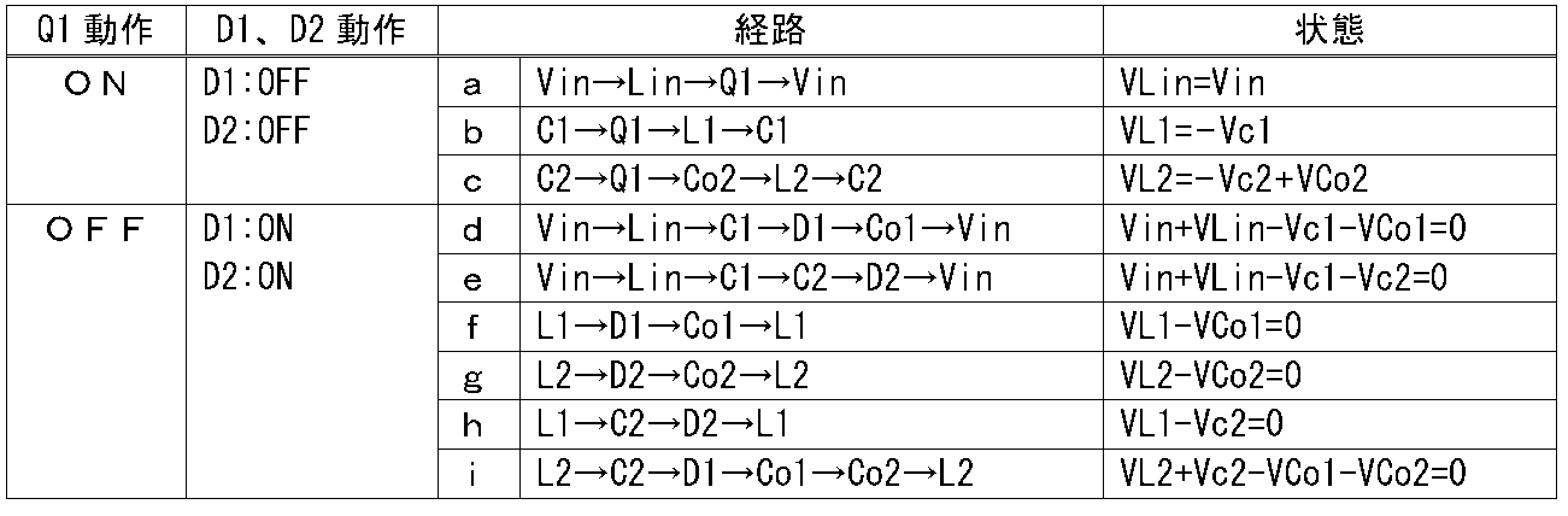
- the discharge path of the positive reactor L1 is the discharge path f of the positive reactor L1 ⁇ diode D1 ⁇ capacitor Co1 ⁇ positive reactor L1.
- a path h of positive reactor L1 ⁇ decoupling capacitor C1 ⁇ decoupling capacitor C2 ⁇ diode D2 ⁇ positive reactor L1 is formed.
- the discharge path of the negative reactor L2 is negative reactor L2 ⁇ decoupling capacitor C2 ⁇ decoupling capacitor C1 ⁇ diode D1 ⁇ capacitor Co1 ⁇
- a path i of capacitor Co2 ⁇ negative reactor L2 is formed.
- VCo1 Vc2-Vc1
- VCo2 VCo1+VCo2+Vc1-Vc2
- the capacitances of the decoupling capacitors C1 and C2 are increased, the voltage of the decoupling capacitor C1 will change to the input voltage Vin and the voltage of the decoupling capacitor C2 because the initial voltages of the decoupling capacitors C1 and C2 are zero volts before power supply operation. becomes equal to Vin+VCo2, or the transient response speed slows down. Therefore, it is desirable to select small capacitances for the decoupling capacitors C1 and C2. However, when the capacitances of the decoupling capacitors C1 and C2 are decreased, the ripple voltages ⁇ Vc1 and ⁇ Vc2 of the decoupling capacitors C1 and C2 are increased.
- the voltage of the decoupling capacitor C1 becomes Vin+ ⁇ Vc1
- the voltage of the decoupling capacitor C2 becomes Vin+VCo2+ ⁇ Vc2. Therefore, when the load current of the decoupling capacitor C1 is large and the load current of the decoupling capacitor C2 is small, or vice versa, the ripple voltages ⁇ Vc1 and ⁇ Vc2 of the decoupling capacitors C1 and C2 are added to the smaller load current. Therefore, there arises a problem that the cross regulation between the positive output voltage VCo1 and the negative output voltage VCo2 is deteriorated. That is, as shown in the cross regulation characteristic diagram of FIG.
- a multi-output SEPIC converter that supplies positive and negative output voltages
- the positive output of the SEPIC converter includes an input side reactor, a first coupling capacitor, and a positive electrode.
- a first smoothing capacitor is connected between the positive output and GND, and a positive output side reactor is connected between a connection point between the first coupling capacitor and the positive rectifier diode and GND. is connected, and the negative output of the SEPIC converter is connected to the connection point of the first coupling capacitor, the positive rectifier diode, and the positive output side reactor via the second coupling capacitor and the negative output side reactor.
- a second smoothing capacitor is connected between the negative output and GND, and the negative rectifier diode is connected between the connection point between the second coupling capacitor and the negative output side reactor and GND.
- cross regulation accuracy can be maintained regardless of the cross load current.
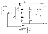
- FIG. 1 is a diagram showing a DC/DC converter configured with a SEPIC circuit according to an embodiment of the present invention.
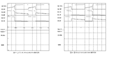
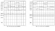
- FIG. 2 is a diagram showing cross regulation characteristics in the embodiment of the invention shown in FIG.
- FIG. 3 is a diagram showing a DC/DC converter of a SEPIC circuit composed of synchronous rectification circuits as an application example of the embodiment of the present invention.
- FIG. 4 illustrates a prior art SEPIC circuit.
- FIG. 5 is a diagram showing cross regulation characteristics in the prior art shown in FIG.
- FIG. 1 The embodiment of FIG. 1 is obtained by removing the diode D3 and the capacitor Co3 from the circuit of the prior art and arranging only two outputs, positive and negative, with the same number of component parts for functions. However, it differs in that the decoupling capacitors C1 and C2 are connected in series. That is, the positive terminal of the decoupling capacitor C2 is connected from the connection point between the input reactor Lin and the drain of the switching element Q1 to the connection point between the decoupling capacitor C1, the anode terminal of the diode D1 and the positive reactor L1.
- the discharge path of the positive reactor L1 is the positive reactor L1 ⁇ diode D1 ⁇ capacitor Co1 ⁇ positive reactor L1.
- a path h of positive reactor L1 ⁇ decoupling capacitor C2 ⁇ diode D2 ⁇ positive reactor L1 is formed.
- the discharge path of the negative reactor L2 is the negative reactor L2 ⁇ diode D2 ⁇ capacitor Co2 ⁇ negative reactor L2 discharge path g. is formed.
- paths passing through the decoupling capacitor C1 were formed in the two additional paths, but in the present invention there is no path passing through the decoupling capacitor C1.
- VCo1 Vc2
- the capacitance of the decoupling capacitor C2 is sufficiently large with respect to the output current, the voltage Vc2 of the decoupling capacitor C2 will be VCo2.
- the voltage drop value due to the ON resistance is small, so that the effect of improving the cross regulation accuracy can be obtained.
- the SEPIC converter according to the present invention is suitable for obtaining multiple positive and negative outputs. Therefore, it can be used as a power source for an in-vehicle device using this.
Landscapes
- Engineering & Computer Science (AREA)
- Power Engineering (AREA)
- Dc-Dc Converters (AREA)
Abstract
Description
また、入力電圧Vinに入力リアクトルLinの回生エネルギーを重畳させて整流することで昇圧電圧+Vout3を得ている。
なお、スイッチング素子Q1のオンオフ駆動信号は、PWM信号生成部Cont1にて、基準電圧Vrefと正極出力電圧+Voutとの誤差信号を演算してフィードバック制御を行っている。
この理由は、下記のように入力電圧とデューティーDの関係が同様になるためである。
上記の関係を数式で表すと、まず正極出力電圧+Vout側は定常状態では入力リアクトルLinの充電・放電が等しくなることから下記の関係式が成り立つ。
Vin・D=(VCo1+Vc1-Vin)・(1-D)
D/(1-D)=(VCo1+Vc1-Vin)/Vin (1)
正極リアクトルL1も同様に充電・放電が等しくなることから
Vc1・D=VCo1・(1-D)
D/(1-D)=VCo1/Vc1 (2)
式(1)、(2)から
(Vout+Vc1-Vin)/Vin=VCo1/Vc1
Vc1・(Vout+Vc1-Vin)-VCo1・Vin=0
Vc1・(Vout+Vc1)-Vc1・Vin-VCo1・Vin=0
Vc1・(Vout+Vc1)-(Vc1+VCo1)・Vin=0
(Vc1-Vin)・(Vc1+VCo1)=0
∴ Vc1=Vin
(ただし、Vc1=-VCo1はダイオードD1のブレークダウンのため、成立しない)
したがって、デカップリングコンデンサC1の電圧はVinとなる。
また、式(1)から
D/(1-D)Vin=(VCo1+Vc1-Vin)
VCo1=Vin・(D/(1-D))+Vin-Vc1
=(VinD+Vin-VinD)/(1-D)-Vc1
=(Vin)/(1-D)-Vc1
ここで、Vc1=Vinから、
VCo1=Vin・D/(1-D)
となる。
また、同様に負極出力電圧-Vout側は、定常状態では入力リアクトルLinの充電・放電が等しくなることから下記の関係式が成り立つ。
Vin・D=(Vc2-Vin)・(1-D)
D/(1-D)=(Vc2-Vin)/Vin (3)
負極出力リアクトルL2も同様に充電・放電が等しくなることから
(Vc2-VCo2)・D=VCo2・(1-D)
D/(1-D)=VCo2/(Vc2-VCo2) (4)
式(3)、(4)から
(Vc2-Vin)/Vin=VCo2/(Vc2-VCo2)
(Vc2-Vin)・(Vc2-VCo2)=Vin・VCo2
Vc22-Vc2・VCo2-Vin・Vc2+Vin・VCo2-Vin・VCo2=0
Vc22 -Vc2・VCo2-Vin・Vc2=0
Vc2(Vc2-VCo2-Vin)=0
Vc2=Vin+VCo2
デカップリングコンデンサC2の電圧は入力電圧Vin+負極出力電圧VCo2となる。
また、式(3)から
D/(1-D)=(Vc2-Vin)/Vin
Vin・D/(1-D)=Vc2-Vin
Vin・D/(1-D)+Vin=Vc2
(Vin・D+Vin-Vin・D)/(1-D)=Vc2
Vin/(1-D)=Vc2 (5)
式(4)から
D/(1-D)=VCo2/(Vc2-VCo2)
D・(Vc2-VCo2)=VCo2(1-D)
D・Vc2-D・VCo2=VCo2-D・VCo2
D・Vc2=VCo2
Vc2=VCo2/D (6)
式(5)、(6)から
Vin/(1-D)=VCo2/D
VCo2=Vin・D/(1-D)
となる。従って、正極出力電圧+Vout(=VCo1)と負極出力電圧-Vout(=VCo2)は同じ電圧が出力される。
また、 負極リアクトルL2の放電経路は負極リアクトルL2→ダイオードD2→コンデンサCo2→負極リアクトルL2の放電経路gの他に、負極リアクトルL2→デカップリングコンデンサC2→デカップリングコンデンサC1→ダイオードD1→コンデンサCo1→コンデンサCo2→負極リアクトルL2の経路iが形成される。

VCo1=Vc2-Vc1
VCo2=VCo1+VCo2+Vc1-Vc2
の関係式が成り立つ。
デカップリングコンデンサC1とC2の静電容量が出力電流に対して十分に大きければ、
デカップリングコンデンサC1の電圧Vc1は入力電圧Vinとなり、
デカップリングコンデンサC2の電圧Vc2はVin+VCo2となるので、
VCo1=Vin+VCo2―Vin=VCo2
となる。
しかしながら、デカップリングコンデンサC1とC2の静電容量を大きくすると、デカップリングコンデンサC1とC2の初期電圧が電源動作前はゼロボルトなので、デカップリングコンデンサC1の電圧が入力電圧VinとデカップリングコンデンサC2の電圧がVin+VCo2と等しくなるまでに時間を要したり、過渡的な応答速度が遅くなったりする。このため、デカップリングコンデンサC1とC2は小さい容量を選択することが望ましい。
しかし、デカップリングコンデンサC1とC2の静電容量を小さくすると、デカップリングコンデンサC1とC2のリップル電圧△Vc1、△Vc2が大きくなる。その結果、デカップリングコンデンサC1の電圧はVin+△Vc1、デカップリングコンデンサC2の電圧はVin+VCo2+△Vc2となる。
したがって、デカップリングコンデンサC1の負荷電流が多く、デカップリングコンデンサC2の負荷電流が少ない場合、またはその逆の時にデカップリングコンデンサC1、C2のリップル電圧△Vc1、△Vc2が負荷電流の少ない方に加算されるため、正極出力電圧VCo1と負極出力電圧VCo2のクロスレギュレーションが悪化するという課題が発生する。
すなわち、図5に示すクロスレギュレーション特性図のように、正負極出力電圧±Voutのクロス負荷電流の条件になると、負荷電流の大きいほうの出力電圧が低下し、反面、負荷電流の小さいほうの出力電圧が上昇し、クロスレグレーションの精度が悪くなる問題がある。
図1の実施例は、従来技術の回路からダイオードD3とコンデンサCo3を削除して正負極の2出力のみに整理したもので、機能に対する構成部品は同じ構成部品点数からなる。
しかし、デカップリングコンデンサC1とC2の接続を直列接続した点で異なる。すなわち、デカップリングコンデンサC2の正極端子を入力リアクトルLinとスイッチング素子Q1のドレインとの接続点から、デカップリングコンデンサC1とダイオードD1アノード端子と正極リアクトルL1との接続点に接続する。
Vin・D=(Vco1+Vc1-Vin)・(1-D)
D/(1-D)=(Vco1+Vc1-Vin)/Vin (7)
正極リアクトルL1も同様に充電・放電が等しくなることから
Vc1・D=VCo1・(1-D)
D/(1-D)=VCo1/Vc1 (8)
ここで式(7)、(8)から
(Vco1+Vc1-Vin)/Vin=VCo1/Vc1
Vc1・(Vco1+Vc1-Vin)―Vco1・Vin=0
Vc1・(Vco1+Vc1)-Vc1・Vin-VCo1・Vin=0
Vc1・(Vco1+Vc1)-(Vc1+VCo1)・Vin=0
(Vc1-Vin)・(Vc+VCo1)=0
∴ Vc1=Vin
(Vc1=-VCo1はダイオードD1のブレークダウンのため、成立しない。)
したがって、デカップリングコンデンサC1の電圧は入力電圧Vinとなる。
また、式(7)から
D/(1-D)・Vin=(VCo1+Vc1-Vin)
VCo1=Vin(D/(1-D) )+Vin-Vc1
=(Vin・D+Vin-Vin・D)/(1-D)-Vc1
=(Vin)/(1-D)-Vc1
Vc1=Vinから、
Vco1=Vin・D/(1-D)
と正極出力電圧+Voutは表せられる。
次に、負極出力電圧-Vout側も同様に、定常状態では入力リアクトルLinの充電・放電が等しくなることから、
Vin・D=(Vc1+Vc2-Vin)・(D-1)
D/(D-1)=(Vc1+Vc2-Vin)/Vin (9)
負極リアクトルL2も同様に充電・放電が等しくなることから
(Vc1+Vc2-VCo2)・D=VCo2・(D-1)
D/(D-1)=VCo2/(Vc1+Vc2-VCo2) (10)
ここで、式(9)、(10)から
(Vc1+Vc2-Vin)/Vin=VCo2/(Vc1+Vc2-VCo2)
(Vc1+Vc2-Vin)・(Vc1+Vc2-VCo2)=Vin・VCo2
Vc1+Vc2=Vin+VCo2
となり、デカップリングコンデンサC1とC2の電圧は入力電圧+出力電圧となる。
デカップリングコンデンサC1の電圧Vc1は、前述のSEPICの動作よりVc1=Vinなので、デカップリングコンデンサC1の電圧Vc1は入力電圧、デカップリングコンデンサC2の電圧Vc2はVCo2となることが分かる。
D/(1-D)=(Vc1+Vc2-Vin)/Vin
Vin・D/(1-D)=Vc1+Vc2-Vin
Vin・D/(1-D)+Vin=Vc1+Vc2
(Vin・D+Vin-Vin・D)/(1-D)=Vc1+Vc2
Vin/(1-D)=Vc1+Vc2 (11)
また、式(8)から
D/(1-D)=Vco2/(Vc1+Vc2-VCo2)
D(Vc1+Vc2-Vco2)=VCo2(1-D)
D・Vc1+D・Vc2-D・Vco2=VCo2-D・Vco2
D・Vc1+D・Vc2=Vco2
Vc1+Vc2= VCo2/D (12)
式(11)、(12)から
Vin/(1-D)= VCo2/D
VCo2=Vin・D/(1-D)
VCo1とVCo2は同じ電圧が出力される。
従って、正極出力電圧+Vout(=VCo1)と負極出力電圧-Vout(=VCo2)は同じ電圧が出力される。
また、 負極リアクトルL2の放電経路は負極リアクトルL2→ダイオードD2→コンデンサCo2→負極リアクトルL2の放電経路gの他に負極リアクトルL2→デカップリングコンデンサC2→ダイオードD1→コンデンサCo1→コンデンサCo2→負極リアクトルL2の経路iが形成される。
従来回路構成では2つの追加経路にデカップリングコンデンサC1を通る経路が形成されていたが、本発明ではデカップリングコンデンサC1を通る経路がなくなった。
ゆえに、
VCo1=Vc2
VCo2=VCo1+VCo2-Vc2
となる。
ここで、デカップリングコンデンサC2の静電容量が出力電流に対して十分に大きければ、デカップリングコンデンサC2の電圧Vc2はVCo2となるので、
VCo1=VCo2=Vc2
となる。
したがって、デカップリングコンデンサC1の静電容量を小さくし、デカップリングコンデンサC2を大きな静電容量にすることで、クロスレギュレーションが改善される。
すなわちデカップリングコンデンサの静電容量はC1のみとなるので、起動時間の改善、負荷応答性の改善は同時に達成できるメリットがある。
例えば、図3に示すようにダイオードD1、D2の代わりにPチャンネルMOSFET
Q2、Q3の同期整流素子に置き換えてもよい。ダイオードを同期整流素子に置き換えることで整流素子の損失低減が得られる。また、出力電流の変動に対するダイオードの順方向電圧特性とPチャンネルMOSFETのON抵抗による電圧降下を比較すると、ON抵抗による電圧降下値が小さいので、クロスレギュレーション精度を向上する効果が得られる。
C1、C2 デカップリングコンデンサ
Co1、Co2、Co3 コンデンサ
Cont1 PWM信号生成部
D1、D2、D3 ダイオード
Lin 入力リアクトル
L1 正極リアクトル
L2 負極リアクトル
Q1 スイッチング素子
Q2、Q3 PチャネルMOSFET
Claims (2)
- 正負出力電圧を供給するマルチ出力SEPICコンバータであって、
前記SEPICコンバータの正極出力は、入力側リアクトルと第1の結合コンデンサと正極整流ダイオードとを介して接続され、正極出力とGND間には第1の平滑コンデンサが接続され、
また、前記第1の結合コンデンサと前記正極整流ダイオードとの接続点とGND間に正極出力側リアクトルが接続され、
前記SEPICコンバータの負極出力は、前記前記第1の結合コンデンサと前記正極整流ダイオードと前記正極出力側リアクトルとの接続点に、第2の結合コンデンサと負極出力側リアクトルとを介して接続され、負極出力とGND間には第2の平滑コンデンサが接続され、
また、前記第2の結合コンデンサと負極出力側リアクトルとの接続点とGND間に前記負極整流ダイオードが接続されたことを特徴とする正負出力電圧を供給するマルチ出力SEPICコンバータ。 - 前記正極整流ダイオードおよび前記負極整流ダイオードは、同期整流素子からなることを特徴とする請求項1記載の正負出力電圧を供給するマルチ出力SEPICコンバータ。
Priority Applications (4)
| Application Number | Priority Date | Filing Date | Title |
|---|---|---|---|
| CN202180095461.XA CN116964918A (zh) | 2021-05-24 | 2021-05-24 | 多输出sepic转换器 |
| JP2023523711A JP7582463B2 (ja) | 2021-05-24 | 2021-05-24 | マルチ出力sepicコンバータ |
| PCT/JP2021/019537 WO2022249227A1 (ja) | 2021-05-24 | 2021-05-24 | マルチ出力sepicコンバータ |
| US18/505,298 US12531482B2 (en) | 2021-05-24 | 2023-11-09 | Multi-output SEPIC converter |
Applications Claiming Priority (1)
| Application Number | Priority Date | Filing Date | Title |
|---|---|---|---|
| PCT/JP2021/019537 WO2022249227A1 (ja) | 2021-05-24 | 2021-05-24 | マルチ出力sepicコンバータ |
Related Child Applications (1)
| Application Number | Title | Priority Date | Filing Date |
|---|---|---|---|
| US18/505,298 Continuation US12531482B2 (en) | 2021-05-24 | 2023-11-09 | Multi-output SEPIC converter |
Publications (1)
| Publication Number | Publication Date |
|---|---|
| WO2022249227A1 true WO2022249227A1 (ja) | 2022-12-01 |
Family
ID=84229605
Family Applications (1)
| Application Number | Title | Priority Date | Filing Date |
|---|---|---|---|
| PCT/JP2021/019537 Ceased WO2022249227A1 (ja) | 2021-05-24 | 2021-05-24 | マルチ出力sepicコンバータ |
Country Status (4)
| Country | Link |
|---|---|
| US (1) | US12531482B2 (ja) |
| JP (1) | JP7582463B2 (ja) |
| CN (1) | CN116964918A (ja) |
| WO (1) | WO2022249227A1 (ja) |
Citations (5)
| Publication number | Priority date | Publication date | Assignee | Title |
|---|---|---|---|---|
| JP2014017931A (ja) * | 2012-07-06 | 2014-01-30 | Asahi Kasei Electronics Co Ltd | Dc−dcコンバータ |
| JP5477946B2 (ja) * | 2008-07-24 | 2014-04-23 | ジーイー・メディカル・システムズ・グローバル・テクノロジー・カンパニー・エルエルシー | 電圧発生回路及び超音波診断装置 |
| US20170302176A1 (en) * | 2016-04-13 | 2017-10-19 | Infineon Technologies Austria Ag | System and Method for a Switched-Mode Power Supply |
| US20170331368A1 (en) * | 2014-12-09 | 2017-11-16 | Robert Bosch Gmbh | Dc-dc converter system, dc voltage supply system and printed circuit board for a dc-dc converter system |
| CN109450252A (zh) * | 2018-12-27 | 2019-03-08 | 西安奇维科技有限公司 | 一种三轨电源生成装置 |
Family Cites Families (10)
| Publication number | Priority date | Publication date | Assignee | Title |
|---|---|---|---|---|
| US10020747B2 (en) | 2014-04-15 | 2018-07-10 | Danmarks Tekniske Universitet | Resonant DC-DC power converter assembly |
| US10097017B2 (en) * | 2015-06-24 | 2018-10-09 | Apple Inc. | Systems and methods for bidirectional two-port battery charging with boost functionality |
| US10186955B2 (en) * | 2015-10-03 | 2019-01-22 | Rompower Technology Holdings, Llc | Ideal switch bridgeless PFC |
| CN106253661B (zh) * | 2016-08-05 | 2018-12-28 | 矽力杰半导体技术(杭州)有限公司 | 控制电路、控制方法及应用其的功率变换器 |
| CN107453603B (zh) * | 2017-09-30 | 2020-05-26 | 湘潭大学 | 一种双输入Sepic变换器 |
| TW201926873A (zh) * | 2017-12-06 | 2019-07-01 | 群光電能科技股份有限公司 | 切換式電源之電路結構 |
| CN108809091B (zh) * | 2018-06-19 | 2020-05-22 | 四川大学 | 一种单开关降压式多路恒流输出开关变换器 |
| EP3913782A4 (en) * | 2019-01-16 | 2022-03-16 | Panasonic Intellectual Property Management Co., Ltd. | DC VOLTAGE CONVERTER |
| CN209767386U (zh) * | 2019-05-08 | 2019-12-10 | 西南交通大学 | 具有双极性输出的四端口变换器 |
| CN111464023B (zh) * | 2020-04-30 | 2023-05-02 | 三峡大学 | 一种高增益升压和降压Sepic DC-DC变换器 |
-
2021
- 2021-05-24 CN CN202180095461.XA patent/CN116964918A/zh active Pending
- 2021-05-24 WO PCT/JP2021/019537 patent/WO2022249227A1/ja not_active Ceased
- 2021-05-24 JP JP2023523711A patent/JP7582463B2/ja active Active
-
2023
- 2023-11-09 US US18/505,298 patent/US12531482B2/en active Active
Patent Citations (5)
| Publication number | Priority date | Publication date | Assignee | Title |
|---|---|---|---|---|
| JP5477946B2 (ja) * | 2008-07-24 | 2014-04-23 | ジーイー・メディカル・システムズ・グローバル・テクノロジー・カンパニー・エルエルシー | 電圧発生回路及び超音波診断装置 |
| JP2014017931A (ja) * | 2012-07-06 | 2014-01-30 | Asahi Kasei Electronics Co Ltd | Dc−dcコンバータ |
| US20170331368A1 (en) * | 2014-12-09 | 2017-11-16 | Robert Bosch Gmbh | Dc-dc converter system, dc voltage supply system and printed circuit board for a dc-dc converter system |
| US20170302176A1 (en) * | 2016-04-13 | 2017-10-19 | Infineon Technologies Austria Ag | System and Method for a Switched-Mode Power Supply |
| CN109450252A (zh) * | 2018-12-27 | 2019-03-08 | 西安奇维科技有限公司 | 一种三轨电源生成装置 |
Also Published As
| Publication number | Publication date |
|---|---|
| JP7582463B2 (ja) | 2024-11-13 |
| US12531482B2 (en) | 2026-01-20 |
| US20240072659A1 (en) | 2024-02-29 |
| CN116964918A (zh) | 2023-10-27 |
| JPWO2022249227A1 (ja) | 2022-12-01 |
Similar Documents
| Publication | Publication Date | Title |
|---|---|---|
| US6756772B2 (en) | Dual-output direct current voltage converter | |
| CN101647182B (zh) | 包括升压电感式开关前置调节器和电容式开关后置转换器的高效dc/dc电压转换器 | |
| CN102771039B (zh) | Dc/dc电力变换装置 | |
| Guo et al. | A family of multimodes charge pump based dc–dc converter with high efficiency over wide input and output range | |
| JP6815127B2 (ja) | Dc/dcコンバータ、スイッチング電源装置 | |
| US8836301B2 (en) | Power supply unit | |
| JP6065262B2 (ja) | 電源装置 | |
| US12003175B2 (en) | Hybrid converter with reduced inductor loss | |
| US11532979B2 (en) | Dual supply low-side gate driver | |
| WO2015137852A1 (en) | Isolated fly-buck converter, switched mode power supply, and method of measuring a voltage on a secondary side of an isolated fly-buck converter | |
| CN102739044A (zh) | Dc/dc升压转换器和led驱动器 | |
| KR20150025486A (ko) | 고승압 소프트 스위칭 직류-직류 컨버터 | |
| Cao et al. | A high voltage gain multilevel modular switched-capacitor DC-DC converter | |
| JP7582463B2 (ja) | マルチ出力sepicコンバータ | |
| JP2013172467A (ja) | スイッチング電源回路 | |
| JP2012080596A (ja) | 圧電素子発電回路 | |
| JP7634833B2 (ja) | スイッチング電源装置 | |
| Kularatna et al. | Very low frequency supercapacitor techniques to improve the end-to-end efficiency of DC-DC converters based on commercial off the shelf LDOs | |
| JP7818231B2 (ja) | 電力変換装置、プログラム | |
| Pawar | Review and performance analysis of inductorless charge pumps for low-power applications | |
| Guo et al. | A multi-modes charge-pump based high efficiency wide input range DC-DC converter | |
| Nurhuda et al. | A three-topology based, wide input range switched-capacitor DC-DC converter with low-ripple and enhanced load line regulations | |
| Martin | A Design of 4.5 W Closed Loop Boost Converter with 45V, 100mA Output for Low Power Applications | |
| JP2009005487A (ja) | 電源システム | |
| Li et al. | A High-Efficiency Boost Converter Based on Synchronous Rectification |
Legal Events
| Date | Code | Title | Description |
|---|---|---|---|
| 121 | Ep: the epo has been informed by wipo that ep was designated in this application |
Ref document number: 21942885 Country of ref document: EP Kind code of ref document: A1 |
|
| ENP | Entry into the national phase |
Ref document number: 2023523711 Country of ref document: JP Kind code of ref document: A |
|
| WWE | Wipo information: entry into national phase |
Ref document number: 202180095461.X Country of ref document: CN |
|
| NENP | Non-entry into the national phase |
Ref country code: DE |
|
| 122 | Ep: pct application non-entry in european phase |
Ref document number: 21942885 Country of ref document: EP Kind code of ref document: A1 |