WO2022234769A1 - アンテナ素子及び電子機器 - Google Patents
アンテナ素子及び電子機器 Download PDFInfo
- Publication number
- WO2022234769A1 WO2022234769A1 PCT/JP2022/017729 JP2022017729W WO2022234769A1 WO 2022234769 A1 WO2022234769 A1 WO 2022234769A1 JP 2022017729 W JP2022017729 W JP 2022017729W WO 2022234769 A1 WO2022234769 A1 WO 2022234769A1
- Authority
- WO
- WIPO (PCT)
- Prior art keywords
- antenna element
- insulating base
- antenna
- conductor layer
- vertical direction
- Prior art date
- Legal status (The legal status is an assumption and is not a legal conclusion. Google has not performed a legal analysis and makes no representation as to the accuracy of the status listed.)
- Ceased
Links
Images











Classifications
-
- H—ELECTRICITY
- H01—ELECTRIC ELEMENTS
- H01Q—ANTENNAS, i.e. RADIO AERIALS
- H01Q13/00—Waveguide horns or mouths; Slot antennas; Leaky-waveguide antennas; Equivalent structures causing radiation along the transmission path of a guided wave
- H01Q13/10—Resonant slot antennas
- H01Q13/106—Microstrip slot antennas
-
- H—ELECTRICITY
- H01—ELECTRIC ELEMENTS
- H01Q—ANTENNAS, i.e. RADIO AERIALS
- H01Q1/00—Details of, or arrangements associated with, antennas
- H01Q1/36—Structural form of radiating elements, e.g. cone, spiral, umbrella; Particular materials used therewith
- H01Q1/38—Structural form of radiating elements, e.g. cone, spiral, umbrella; Particular materials used therewith formed by a conductive layer on an insulating support
-
- H—ELECTRICITY
- H01—ELECTRIC ELEMENTS
- H01Q—ANTENNAS, i.e. RADIO AERIALS
- H01Q1/00—Details of, or arrangements associated with, antennas
- H01Q1/40—Radiating elements coated with or embedded in protective material
Definitions
- the present invention relates to an antenna element provided with an antenna conductor layer.
- the microstrip antenna described in Patent Document 1 As an invention related to conventional antenna elements, for example, the microstrip antenna described in Patent Document 1 is known.
- This microstrip antenna comprises a dielectric substrate, a rectangular conductor and a ground conductor.
- the dielectric substrate has an upper major surface and a lower major surface.
- a rectangular conductor is provided on the upper main surface of the dielectric substrate.
- a ground conductor is provided on the lower main surface of the dielectric substrate.
- the rectangular conductor overlaps the ground conductor when viewed in the vertical direction.
- a rectangular conductor functions as an antenna.
- electric field concentration may occur at the outer edge of the rectangular conductor when viewed in the vertical direction.
- electric field concentration occurs, for example, electric field coupling between the conductors existing around the rectangular conductor and the rectangular conductor is likely to occur.
- electromagnetic waves are likely to be radiated from the rectangular conductor toward conductors present around the rectangular conductor.
- the radiation efficiency of the microstrip antenna is reduced.
- an object of the present invention is to provide an antenna element and an electronic device capable of suppressing a decrease in the radiation efficiency of the antenna element.
- An antenna element includes: An antenna element, an insulating base material having a first principal surface and a second principal surface aligned in the vertical direction; one or more antenna conductor layers provided on the first main surface of the insulating base; and an insulating base non-formed region is positioned between the insulating base and the antenna conductor layer in the vertical direction;
- the insulating base does not exist in the insulating base non-formation region, at least a portion of the outer edge of the one or more antenna conductors overlaps the insulating base non-formed region when viewed in the vertical direction and is not in contact with the insulating base;
- the antenna element has the structure (A) or (B), and (A) the one or more insulating base non-forming regions are voids, and (B) the one or more insulating bases.
- a low dielectric constant material having a dielectric constant lower than that of the insulating substrate is provided in the non-forming region.
- the antenna element and the electronic device according to the present invention it is possible to suppress the deterioration of the radiation efficiency of the antenna element.
- FIG. 1 is an exploded perspective view of the antenna element 10.
- FIG. FIG. 2 is a cross-sectional view along AA in FIG.
- FIG. 3 is a flow chart showing the manufacturing process of the antenna element 10.
- FIG. 4 is a cross-sectional view of the antenna element 10a.
- FIG. 5 is a top view of the insulator layer 16a of the antenna element 10b.
- FIG. 6 is a top view of the insulator layer 16a of the antenna element 10c.
- FIG. 7 is a cross-sectional view of the antenna element 10c.
- FIG. 8 is a top view of the insulator layer 16a of the antenna element 10d.
- FIG. 9 is a cross-sectional view of the antenna element 10d.
- FIG. 10 is a cross-sectional view of the antenna element 10d.
- FIG. 11 is a cross-sectional view of the antenna element 10e.
- FIG. 12 is a cross-sectional view of the antenna element 10f.
- FIG. 13 is a top view of the insulator layer 16a of the antenna element 10g.
- FIG. 14 is a cross-sectional view of the antenna element 10g.
- FIG. 15 is a cross-sectional view of the antenna element 10h.
- FIG. 16 is a cross-sectional view of the antenna element 10i.
- FIG. 17 is a top view of the antenna element 10i.
- FIG. 18 is a cross-sectional view of the antenna element 10i during manufacture.
- FIG. 19 is a cross-sectional view of the antenna element 10j.
- FIG. 11 is a cross-sectional view of the antenna element 10e.
- FIG. 12 is a cross-sectional view of the antenna element 10f.
- FIG. 13 is a top view of the
- FIG. 20 is a cross-sectional view of the antenna element 10j during manufacture.
- FIG. 21 is a cross-sectional view of the antenna element 10k.
- FIG. 22 is a cross-sectional view of the antenna element 10l.
- FIG. 23 is a cross-sectional view of the antenna element 10m.
- FIG. 24 is a cross-sectional view of the antenna element 10n.
- FIG. 25 is a cross-sectional view of the antenna element 10o.
- FIG. 26 is an exploded perspective view of the antenna element 10p.
- 27 is a rear view of the circuit board 200.
- FIG. FIG. 28 is a cross-sectional view of the hole Sp0a.
- FIG. 29 is a cross-sectional view of the hole Sp0b.
- FIG. 30 is a cross-sectional view of the hole Sp0c.
- FIG. 31 is a cross-sectional view of the hole Sp0d.
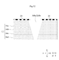
- FIG. 32 is a cross-sectional view of the hole Sp0e.
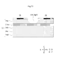
- FIG. 33 is a cross-sectional view of the hole Sp0f.
- FIG. 34 is a cross-sectional view of the hole Sp0g.
- FIG. 1 is an exploded perspective view of the antenna element 10.
- FIG. 1 is an exploded perspective view of the antenna element 10.
- FIG. 2 is a cross-sectional view of the electronic device 1 including the antenna element 10. As shown in FIG. FIG. 2 is a cross-sectional view along AA in FIG. However, FIG. 2 shows the housing 100 that is not shown in FIG.
- the vertical direction is defined as the direction in which the normal lines of the upper and lower main surfaces of the insulating base material 12 of the antenna element 10 extend.
- the vertical direction coincides with the stacking direction of the insulating base material 12 .
- the direction in which the long side of the antenna conductor layer 20 of the antenna element 10 extends is defined as the horizontal direction.
- the direction in which the short side of the antenna conductor layer 20 of the antenna element 10 extends is defined as the front-rear direction.
- the up-down direction is perpendicular to the front-rear direction.
- the left-right direction is orthogonal to the up-down direction and the front-rear direction.
- X is a part or member of the antenna element 10.
- each part of X is defined as follows.
- front of X is meant the front half of X.
- Back of X means the back half of X.
- the left part of X means the left half of X.
- the right part of X means the right half of X.
- Top of X means the top half of X.
- the lower part of X means the lower half of X.
- the leading edge of X means the leading edge of X.
- the trailing end of X means the trailing end of X.
- the left end of X means the end of X in the left direction.
- the right end of X means the end of X in the right direction.
- the upper end of X means the end of X in the upward direction.
- the lower end of X means the lower end of X.
- the front end of X means the front end of X and its vicinity.
- the rear end of X means the rear end of X and its vicinity.
- the left end of X means the left end of X and its vicinity.
- the right end of X means the right end of X and its vicinity.
- the upper end of X means the upper end of X and its vicinity.
- the lower end of X means the lower end of X and its vicinity.
- the antenna element 10 includes an insulating base material 12, an antenna conductor layer 20, reference conductor layers 22, 24 and 26, a signal conductor layer 28, a plurality of interlayer connection conductors v1 and interlayer connection conductors v2. there is
- the insulating base material 12 has a plate shape. Therefore, the insulating base material 12 has an upper principal surface (first principal surface) and a lower principal surface (second principal surface) which are aligned in the vertical direction.
- the upper main surface and the lower main surface of the insulating base material 12 have a rectangular shape with long sides extending in the left-right direction. Therefore, the length of the insulating base material 12 in the left-right direction is longer than the length of the insulating base material 12 in the front-rear direction.
- the insulating base material 12 includes insulator layers 16a to 16e, as shown in FIG.
- the insulating base material 12 has a structure in which insulating layers 16a to 16e are stacked vertically.
- the insulator layers 16a-16e are arranged in this order from top to bottom.
- the insulator layers 16a to 16e have the same rectangular shape as the insulating base material 12 when viewed in the vertical direction.
- the insulator layers 16a-16e are flexible dielectric sheets.
- the material of the insulating base material 12 is, for example, a thermoplastic resin.
- Thermoplastic resins are, for example, thermoplastic resins such as liquid crystal polymer and PTFE (polytetrafluoroethylene).
- the material of the insulating base material 12 may be polyimide.
- the insulating base material 12 has flexibility. Therefore, the antenna element 10 may be used while being bent. “The antenna element 10 is bent” means that the antenna element 10 is deformed and bent by applying an external force to the antenna element 10 .
- the deformation may be elastic deformation, plastic deformation, or both elastic deformation and plastic deformation.
- the antenna conductor layer 20 is provided on the upper main surface or the lower main surface of the insulating base material 12 .
- the antenna conductor layer 20 is provided on the upper main surface of the insulating base material 12 .
- the antenna conductor layer 20 is provided on the upper main surface of the insulator layer 16a (first insulator layer).
- the antenna conductor layer 20 has a rectangular shape with long sides extending in the horizontal direction when viewed in the vertical direction.
- the antenna conductor layer 20 resonates on both the short side extending in the front-rear direction and the long side extending in the left-right direction.
- the short side extending in the front-rear direction and the long side extending in the left-right direction of the antenna conductor layer 20 are about half the wavelength of the high-frequency signal transmitted and received by the antenna conductor layer 20 .
- the length of the wavelength of the high-frequency signal transmitted and received by the antenna conductor layer 20 is the wavelength in consideration of the wavelength shortening effect due to the dielectric constant of the insulating base material 12 .
- the antenna conductor layer 20 radiates high frequency signals as electromagnetic waves. Further, the antenna conductor layer 20 receives high-frequency signals of electromagnetic waves.
- the signal conductor layer 28 is provided on the insulating base material 12 .
- the signal conductor layer 28 is provided on the upper main surface of the insulator layer 16c.
- the signal conductor layer 28 has a linear shape extending in the left-right direction. The right end portion of the signal conductor layer 28 overlaps the antenna conductor layer 20 when viewed in the vertical direction.
- the signal conductor layer 28 transmits high frequency signals.
- the interlayer connection conductor v2 electrically connects the antenna conductor layer 20 and the signal conductor layer . More specifically, the interlayer connection conductor v2 penetrates the insulator layers 16a and 16b in the vertical direction. An upper end of the interlayer connection conductor v2 is connected to the antenna conductor layer 20 . The position where the interlayer connection conductor v2 is connected in the antenna conductor layer 20 is a feeding point for high frequency signals. The lower end of the interlayer connection conductor v2 is connected to the right end of the signal conductor layer 28 .
- the reference conductor layer 22 is provided on the insulating base material 12 and below the antenna conductor layer 20 .
- the reference conductor layer 22 is provided on the lower main surface of the insulator layer 16e.
- the reference conductor layer 22 overlaps the antenna conductor layer 20 when viewed in the vertical direction.
- the reference conductor layer 22 has a rectangular shape with long sides extending in the horizontal direction when viewed in the vertical direction.
- the reference conductor layer 22 protrudes from the antenna conductor layer 20 in the front-rear direction and the left-right direction when viewed in the vertical direction. That is, the outer edge of the reference conductor layer 22 includes the outer edge of the antenna conductor layer 20 when viewed in the vertical direction.
- the reference conductor layer 24 is provided on the insulating base material 12 .
- the reference conductor layer 24 is provided on the upper main surface of the insulating base 12 when the antenna conductor layer 20 is provided on the upper main surface of the insulating base 12 .
- the reference conductor layer 24 is provided on the upper main surface of the insulating base material 12 .
- the reference conductor layer 24 is provided on the upper main surface of the insulator layer 16a on which the antenna conductor layer 20 is provided.
- the reference conductor layer 24 has a rectangular frame shape when viewed in the vertical direction.
- the reference conductor layer 24 surrounds the antenna conductor layer 20 when viewed in the vertical direction.
- the antenna conductor layer 20 and the reference conductor layer 24 are separated from each other so that the antenna conductor layer 20 and the reference conductor layer 24 are not short-circuited.
- the reference conductor layer 26 is provided on the insulating base material 12 .
- the reference conductor layer 26 is provided on the upper main surface of the insulator layer 16c.
- the shape of the reference conductor layer 26 is substantially the same as that of the reference conductor layer 24 .
- the reference conductor layer 26 is not in contact with the signal conductor layer 28 so that the reference conductor layer 26 and the signal conductor layer 28 are not short-circuited.
- a plurality of interlayer connection conductors v1 electrically connect the reference conductor layer 22, the reference conductor layer 24, and the reference conductor layer . More specifically, the plurality of interlayer connection conductors v1 vertically penetrate through the insulator layers 16a to 16e. Upper ends of the plurality of interlayer connection conductors v1 are connected to the reference conductor layer 24 . Middle portions of the plurality of interlayer connection conductors v1 are connected to the reference conductor layer 26 . Lower ends of the plurality of interlayer connection conductors v1 are connected to the reference conductor layer 22 .
- the plurality of interlayer connection conductors v1 are arranged along the reference conductor layer 24 when viewed in the vertical direction. That is, the plurality of interlayer connection conductors v1 are arranged so as to surround the antenna conductor layer 20 when viewed in the vertical direction.
- the antenna conductor layer 20, the reference conductor layers 22, 24, 26, and the signal conductor layer 28 as described above are formed by, for example, etching a metal foil provided on the upper or lower main surface of the insulator layers 16a to 16e. It is formed by being The metal foil is, for example, copper foil.
- the interlayer connection conductors v1 and v2 are, for example, via-hole conductors.
- the via-hole conductors are produced by forming through-holes in the insulating layers 16a to 16e, filling the through-holes with a conductive paste, and solidifying the conductive paste by heating.
- the interlayer connection conductors v1 and v2 may be, for example, through-hole conductors. Through-hole conductors are produced by forming through-holes penetrating all or part of the insulator layers 16a to 16e and plating the through-holes.
- the insulating base material non-formation region A0 and the holes Sp0 will be described.
- the insulating base material non-forming area A0 is formed by partially recessing the upper main surface of the insulating base material 12 downward.
- the insulating base non-formation region A0 is positioned between the insulating base 12 and the antenna conductor layer 20 in the vertical direction. That is, the plurality of insulating base non-formation regions A0 are provided between the insulator layer 16a and the antenna conductor layer 20 in the vertical direction.
- the insulating base non-formation region A0 is positioned below the antenna conductor layer 20 and the reference conductor layer 24.
- the insulating base material 12 does not exist in the insulating base material non-formation area A0.
- the insulating base non-formation region A0 is the vacancy Sp0.
- the outer edge E1 of the antenna conductor layer 20 means an edge positioned outside the antenna conductor layer 20 when viewed in the vertical direction.
- the antenna conductor layer 20 does not exist outside the outer edge E1 of the antenna conductor layer 20 .
- the outer edge E1 has a rectangular shape.
- the inner edge E2 of the reference conductor layer 24 means an edge located inside the reference conductor layer 24 when viewed in the vertical direction.
- the inner edge E2 of the reference conductor layer 24 is positioned within the area surrounded by the outer edge of the reference conductor layer 24 .
- the reference conductor layer 24 exists outside the inner edge E2 of the reference conductor layer 24 .
- the inner edge E2 has a rectangular shape.
- the inner edge E2 surrounds the outer edge E1 when viewed in the vertical direction. Also, the distance between the inner edge E2 and the outer edge E1 is constant.
- a conductor non-formation area A11 is formed between the outer edge E1 of the antenna conductor layer 20 and the inner edge E2 of the reference conductor layer 24 .
- the conductor non-formation area A11 is an area in which no conductor exists.
- the conductor non-formation area A11 has a rectangular frame shape when viewed in the vertical direction.
- the insulating base non-formation region A0 and the holes Sp0 are along the outer edge E1 of the antenna conductor layer 20 and the inner edge E2 of the reference conductor layer 24 when viewed in the vertical direction. That is, the insulating base non-formation region A0 and the holes Sp0 overlap the conductor non-formation region A11 when viewed in the vertical direction. Therefore, the insulating base material non-formation region A0 and the holes Sp0 have a rectangular frame shape when viewed in the vertical direction. Thus, the insulating base non-formation region A0 and the holes Sp0 surround the antenna conductor layer 20 when viewed in the vertical direction. In addition, the reference conductor layer 24 surrounds the insulating base non-formed region A0 and the holes Sp0 when viewed in the vertical direction.
- the insulating base non-formation region A0 and the inner edge P1 of the hole Sp0 overlap the antenna conductor layer 20 when viewed in the vertical direction.
- a hole Sp0 exists between the outer edge E1 of the antenna conductor layer 20 and the insulating base material 12.
- the entire outer edge E ⁇ b>1 of the antenna conductor overlaps the insulating base material non-formation region A ⁇ b>0 when viewed in the vertical direction and is not in contact with the insulating base material 12 .
- the outer edges P2 of the insulating base non-formation region A0 and the holes Sp0 overlap the reference conductor layer 24 when viewed in the vertical direction.
- a hole Sp0 exists between the inner edge E2 of the reference conductor layer 24 and the insulating base material 12.
- the entire inner edge E2 of the reference conductor layer 24 overlaps the insulating base non-formed region A0 when viewed in the vertical direction, and is not in contact with the insulating base 12 .
- a plurality of first openings Op1 are provided in the antenna conductor layer 20 .
- the plurality of first openings Op1 are arranged in a matrix when viewed in the vertical direction.
- the multiple first openings Op1 have annular outer edges when viewed in the vertical direction.
- the plurality of first openings Op1 have circular outer edges when viewed in the vertical direction.
- an annular shape is not limited to a circular ring, and includes a rectangular shape and a triangular shape.
- the annular outer rim has no edges. Therefore, the first opening Op1 does not include a notch.
- the outer edge of the notch has edges.
- the outer edge of the notch is a part of the outer edge of the antenna conductor layer 20 that is bent toward the center of the antenna conductor layer 20 . Therefore, the outer edge of the notch is part of the antenna conductor layer 20 .
- the antenna conductor layer 20 does not exist within the first opening Op1.
- the interval between the plurality of adjacent first openings Op1 is, for example, 1/4 or less of the length of the wavelength of the high-frequency signal transmitted and received by the antenna conductor layer 20 .
- a plurality of first insulating base non-formation regions A1 are provided on the insulating base 12 .
- the plurality of first insulating base non-formation regions A1 are provided in the insulator layer 16a.
- the plurality of first insulating base non-formation regions A1 are positioned below the antenna conductor layer 20 .
- the insulating base material 12 does not exist in the plurality of first insulating base non-formed regions A1.
- the plurality of first insulating base non-formation regions A1 are the first holes Sp1.
- the plurality of first insulating base non-formation regions A1 are arranged in a matrix when viewed in the vertical direction so as to correspond to the plurality of first openings Op1.
- the plurality of first insulating base non-formation regions A1 have annular outer edges when viewed in the vertical direction.
- the plurality of first insulating base non-formation regions A1 have circular outer edges when viewed in the vertical direction.
- each of the plurality of first insulating base non-formation regions A1 includes each of the plurality of first openings Op1 when viewed in the vertical direction. That is, each of the plurality of first openings Op1 does not protrude from the plurality of first insulating base non-formation regions A1. Therefore, the diameter of the first insulating base non-formation region A1 is larger than the diameter of the first opening Op1.
- the first insulating base non-formation region A1 has a hemispherical shape.
- the plurality of second openings Op2, the plurality of second insulating base non-formation regions A2, and the plurality of second holes Sp2 will be described.
- the plurality of second openings Op2, the plurality of second insulating base non-forming regions A2, and the plurality of second holes Sp2 are formed by the plurality of first openings Op1, the plurality of first insulating base non-forming regions A1, and the plurality of second openings Op2. It has a vertically symmetrical structure with one vacancy Sp1. Therefore, description of the plurality of second openings Op2, the plurality of second insulating base non-formation regions A2, and the plurality of second holes Sp2 will be omitted.
- the electronic device 1 includes an antenna element 10 and a housing 100, as shown in FIG. Antenna element 10 is housed in housing 100 .
- the electronic device 1 is, for example, a mobile wireless communication terminal such as a smart phone.
- FIG. 3 is a flow chart showing the manufacturing process of the antenna element 10. As shown in FIG.
- insulator layers 16a to 16c with metal foil attached to the upper main surface are prepared.
- insulator layers 16d and 16e having metal foil attached to their lower main surfaces are prepared (step S1).
- a mask is formed on the metal foil and etching is performed to form the antenna conductor layer 20, the reference conductor layers 22, 24 and 26 and the signal conductor layer 28 on the insulator layers 16a to 16e (step S2). .
- a plurality of interlayer connection conductors v1 and interlayer connection conductors v2 are formed on the insulator layers 16a to 16e (step S3). Specifically, the insulator layers 16a to 16e are irradiated with a laser beam to form a plurality of through holes. After that, the plurality of through holes are filled with a conductive paste.
- the insulating base material 12 is formed by crimping the insulator layers 16a to 16e (step S4, crimping step).
- the insulator layers 16a to 16e are heated while being pressed vertically.
- the insulator layers 16a to 16e are softened, and the insulator layers 16a to 16e are integrated.
- the conductive paste is solidified by heating to form a plurality of interlayer connection conductors v1 and interlayer connection conductors v2.
- vacancies Sp0, a plurality of first vacancies Sp1, and a plurality of second vacancies Sp2 are formed in the insulator layers 16a and 16e (step S5). Specifically, by etching the insulator layer 16a using the antenna conductor layer 20 as a mask, the holes Sp0 and the plurality of first holes Sp1 are formed (first hole forming step). Furthermore, by etching the insulator layer 16e using the reference conductor layer 22 as a mask, a plurality of second holes Sp2 are formed (second hole forming step). Through the above steps, the antenna element 10 is completed.
- the outer edge E ⁇ b>1 of the antenna conductor layer 20 overlaps the insulating base material non-formed area A ⁇ b>0 when viewed in the vertical direction and is not in contact with the insulating base material 12 .
- the insulating base non-formation region A0 is the hole Sp0.
- the dielectric constant around the outer edge E1 of the antenna conductor layer 20 is lowered. Therefore, the occurrence of electric field concentration at the outer edge E1 of the antenna conductor layer 20 is suppressed.
- electric field coupling between the antenna conductor layer 20 and the reference conductor layer 24 is suppressed.
- the radiation of electromagnetic waves from the antenna conductor layer 20 toward the reference conductor layer 24 is suppressed, and the deterioration of the radiation efficiency of the microstrip antenna is suppressed.
- the deterioration of the radiation efficiency of the antenna element 10 can be suppressed also for the following reasons.
- the inner edge E2 of the reference conductor layer 24 overlaps the insulating base non-formed region A0 when viewed in the vertical direction, and is not in contact with the insulating base 12 .
- the insulating base non-formation region A0 is the hole Sp0.
- the dielectric constant around the inner edge E2 of the reference conductor layer 24 is lowered. Therefore, the occurrence of electric field concentration at the inner edge E2 of the reference conductor layer 24 is suppressed.
- electric field coupling between the antenna conductor layer 20 and the reference conductor layer 24 is suppressed.
- the radiation of electromagnetic waves from the antenna conductor layer 20 toward the reference conductor layer 24 is suppressed, and the deterioration of the radiation efficiency of the microstrip antenna is suppressed.
- each of the plurality of first insulating base non-formation regions A1 is located below the antenna conductor layer 20 .
- Each of the plurality of second insulating base non-formation regions A2 is located on the reference conductor layer 22 .
- the plurality of first insulating base non-formation regions A1 and the plurality of second insulating base non-formation regions A2 are first holes Sp1 and second holes Sp2, respectively. This reduces the dielectric constant of the region between the antenna conductor layer 20 and the reference conductor layer 22 . Therefore, the distance between the antenna conductor layer 20 and the reference conductor layer 22 can be shortened in order to form the designed capacitance between the antenna conductor layer 20 and the reference conductor layer 22 . As a result, the thickness of the antenna element 10 can be reduced.
- the antenna element 10 can be easily bent. More specifically, in the antenna element 10, the insulating base 12 is provided with a plurality of first holes Sp1, a plurality of second holes Sp2, and a hole Sp0. This makes it easier for the antenna element 10 to deform. In addition, since the thickness of the antenna element 10 can be reduced as described above, the antenna element 10 can be more easily deformed. As a result, according to the antenna element 10, the antenna element 10 can be easily bent.
- the radiation efficiency of the antenna element 10 can be improved. More specifically, as described above, since the dielectric constant near the antenna conductor layer 20 becomes smaller, the wavelength of the high-frequency signal transmitted through the antenna conductor layer 20 becomes longer. Therefore, the size of the antenna conductor layer 20 may be increased in order to resonate the high-frequency signal in the antenna conductor layer 20 . When the antenna conductor layer 20 is enlarged, the radiation efficiency of the antenna element 10 is improved.
- the holes Sp0 can be easily formed. More specifically, the holes Sp0 are formed by etching the insulator layer 16a using the antenna conductor layer 20 and the reference conductor layer 24 as masks. By using the antenna conductor layer 20 and the reference conductor layer 22 as masks in this way, it is not necessary to form a new mask for forming the holes Sp0. As a result, according to the manufacturing method of the antenna element 10, the holes Sp0 can be easily formed.
- the material of the insulating base material 12 is a thermoplastic resin, it is not necessary to use an adhesive layer made of a material different from the thermoplastic resin for joining the insulating layers 16a to 16e. Thereby, the insulating base material 12 can be easily formed by thermocompression bonding. Moreover, the insulating base material 12 can be easily plastically deformed.
- FIG. 4 is a cross-sectional view of the antenna element 10a.
- the antenna element 10a differs from the antenna element 10 in the following three points.
- a low dielectric constant material 30 having a dielectric constant lower than that of the insulating base material 12 is provided in the plurality of first insulating base non-forming regions A1.
- a low dielectric constant material 32 having a dielectric constant lower than that of the insulating base material 12 is provided in the plurality of second insulating base non-formation regions A2.
- a low dielectric constant material 34 having a lower dielectric constant than the dielectric constant of the insulating base material 12 is provided in the insulating base non-formation region A0.
- the low dielectric constant materials 30, 32, 34 are, for example, materials in which low dielectric ceramic powder is mixed with resin.
- the rest of the structure of the antenna element 10a is the same as that of the antenna element 10, so the description is omitted.
- the antenna element 10a as described above has the same effects as the antenna element 10 does.
- the method for manufacturing the antenna element 10a further includes steps S6 and S7 in FIG. More specifically, each of the low dielectric constant materials 30 and 34 having a dielectric constant lower than that of the insulating base material 12 is filled into the plurality of first holes Sp1 and Sp0 (step S6, first filling step ). Furthermore, the low dielectric constant material 32 having a dielectric constant lower than that of the insulating base material 12 is filled into the plurality of second holes Sp2 (step S7, second filling step). In the first filling step and the second filling step, for example, each of the pastes of the low dielectric constant materials 30, 32, and 34 is squeegeeed into the plurality of first holes Sp1, the plurality of second holes Sp2, and the holes Sp0.
- FIG. 5 is a top view of the insulator layer 16a of the antenna element 10b.
- the antenna element 10b differs from the antenna element 10 in the structure of the antenna conductor layer 20, the number and shape of the first openings Op1, and the number and shape of the first insulating base non-formation regions A1. More specifically, the antenna conductor layer 20 and the reference conductor layer 24 are integrated. Thereby, the ground potential is connected to the antenna conductor layer 20 .
- the antenna element 10b has one first aperture Op1.
- the number of first insulating base non-formation regions A1 is one.
- the first opening Op1 has a belt shape extending in the front-rear direction when viewed in the vertical direction. The length of the first opening Op1 in the front-rear direction is approximately half the wavelength of the high-frequency signal transmitted and received by the antenna conductor layer 20 .
- the first insulating base non-formation region A1 has a strip shape extending in the front-rear direction when viewed in the vertical direction.
- the signal conductor layer 28 overlaps the first opening Op1 when viewed in the vertical direction.
- the signal conductor layer 28 is not connected to the antenna conductor layer 20 via an interlayer connection conductor.
- the antenna conductor layer 20 functions as a slot antenna.
- the rest of the structure of the antenna element 10b is the same as that of the antenna element 10, so the description is omitted. According to the antenna element 10b, the same effects as those of the antenna element 10 can be obtained.
- FIG. 6 is a top view of the insulator layer 16a of the antenna element 10c.
- FIG. 7 is a cross-sectional view of the antenna element 10c.
- the antenna element 10c differs from the antenna element 10 in that it includes a plurality of antenna conductor layers 20a to 20o.
- the antenna conductor layers 20a to 20o are provided on the upper main surface of the insulating base material 12. As shown in FIG. Accordingly, the antenna conductor layers 20a to 20o are provided on the upper main surface of the insulator layer 16a.
- the antenna conductor layers 20a to 20o are arranged in a matrix when viewed in the vertical direction. Although illustration is omitted, the antenna conductor layers 20a to 20o are electrically connected to signal conductor layers (not shown) via interlayer connection conductors v100. Since other structures of the antenna element 10c are the same as those of the antenna element 10, description thereof is omitted.
- the same effects as those of the antenna element 10 can be obtained. Further, by providing the first insulating base non-formation region A1 between the antenna conductor layers 20a to 20o, interference of high frequency signals between the antenna conductor layers 20a to 20o is suppressed. Furthermore, since the antenna conductor layers 20a to 20o can be brought closer, the size of the antenna element 10c can be reduced.
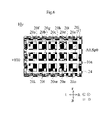
- FIG. 8 is a top view of the insulator layer 16a of the antenna element 10d.
- 9 and 10 are cross-sectional views of the antenna element 10d.
- the antenna element 10d differs from the antenna element 10 in that it includes antenna conductor layers 20a and 20b and reference conductor layers 22a and 22b.
- the antenna conductor layers 20a and 20b are provided on the upper main surface of the insulator layer 16a.
- the antenna conductor layers 20a and 20b are arranged in this order from left to right.
- the reference conductor layers 22a and 22b are provided on the lower main surface of the insulator layer 16e.
- the reference conductor layers 22a and 22b are provided in this order from left to right.
- the reference conductor layers 22a and 22b are electrically connected by conductor layers and interlayer connection conductors (not shown).
- This conductor layer is provided on the upper main surface of the insulator layer 16c.
- the reference conductor layers 22a, 22b, and 24 are electrically connected by conductor layers and interlayer connection conductors (not shown).
- the antenna element 10d has first sections A21, A23 and a second section A22.
- the first section A21, the second section A22 and the first section A23 are arranged in this order from left to right.
- the second section A22 is bent with respect to the first section A21 in the negative direction of the z-axis (vertical direction in the first section A21).
- the radius of curvature of the second section A22 is smaller than the radius of curvature of the first sections A21 and A23.
- the first sections A21 and A23 are not bent in the z-axis direction.
- the insulating base non-formed area A0 is located in the second section A22.
- the hole Sp0 is located in the second section A22.
- the insulating base non-formed region A0 and the holes Sp0 reach the signal conductor layer 28 .
- the insulating base material 12 is further provided with an insulating base material non-formation region A10 and holes Sp10.
- the insulating base non-formed region A10 and the holes Sp10 reach the signal conductor layer 28 .
- the vertical thickness of the antenna element 10d in the first sections A21 and A23 is greater than the vertical thickness of the antenna element 10d in the second section A22.
- the antenna element 10d can be easily bent in the z-axis direction in the second section A22.
- the rest of the structure of the antenna element 10d is the same as that of the antenna element 10, so description thereof will be omitted. According to the antenna element 10d, the same effect as the antenna element 10 can be obtained.
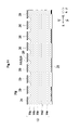
- FIG. 11 is a cross-sectional view of the antenna element 10e.
- the insulating base non-formed region A0 and the holes Sp0 do not reach the signal conductor layer 28, and the insulating base non-formed region A10 and the holes Sp10 reach the signal conductor layer 28. It differs from the antenna element 10d in that it does not.
- the rest of the structure of the antenna element 10e is the same as that of the antenna element 10d, so the description is omitted.
- the antenna element 10e can achieve the same effects as the antenna element 10d.
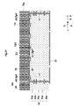
- FIG. 12 is a cross-sectional view of the antenna element 10f.
- the antenna element 10f differs from the antenna element 10e in that the insulating base non-formation region A10 and the air holes Sp10 are not provided. Since other structures of the antenna element 10f are the same as those of the antenna element 10e, description thereof is omitted.
- the antenna element 10f can provide the same effects as the antenna element 10e.
- FIG. 13 is a top view of the insulator layer 16a of the antenna element 10g.
- FIG. 14 is a cross-sectional view of the antenna element 10g.
- the antenna element 10 g differs from the antenna element 10 in the shape of the antenna conductor layer 20 and the shape of the reference conductor layer 24 . More specifically, the antenna conductor layer 20 has a meandering shape when viewed in the vertical direction. That is, the antenna conductor layer 20 meanders when viewed in the vertical direction. Further, the reference conductor layer 24 has an L shape when viewed in the vertical direction. Specifically, the reference conductor layer 24 extends in the front-rear direction on the left of the antenna conductor layer 20 and extends in the left-right direction behind the antenna conductor layer 20 . Since other structures of the antenna element 10g are the same as those of the antenna element 10, description thereof is omitted. According to the antenna element 10g, the same effects as those of the antenna element 10 can be obtained.
- the electrical length of the antenna conductor layer 20 is increased. Therefore, the frequency of the high-frequency signal that resonates in the antenna conductor layer 20 is lowered.
- FIG. 15 is a cross-sectional view of the antenna element 10h.
- the antenna element 10h differs from the antenna element 10 in that a protective layer 102 is further provided.
- the antenna conductor layer 20 is provided on the upper main surface of the insulating base material 12 .
- the protective layer 102 covers the antenna conductor layer 20 and is provided on the upper main surface of the insulating base material 12 .
- the material of the protective layer 102 is different from the material of the insulator layers 16a-16e. Accordingly, protective layer 102 is not part of insulating substrate 12 .
- the Young's modulus of the material of the protective layer 102 is, for example, greater than that of the material of the insulator layers 16a to 16e. Since other structures of the antenna element 10h are the same as those of the antenna element 10, description thereof is omitted. According to the antenna element 10h, the same effect as the antenna element 10 can be obtained.
- the antenna conductor layer 20 is protected and the structure of the holes Sp0 is protected. Further, when the dielectric constant of the protective layer 102 is higher than the dielectric constant of the insulator layers 16a to 16e, the frequency band of high-frequency signals that can be communicated by the antenna element 10h is widened. If the thickness of the protective layer 102 in the vertical direction is approximately the same as the wavelength of the high-frequency signal, the dielectric constant of the protective layer 102 may be lower than that of the insulating layers 16a to 16e.
- FIG. 16 is a cross-sectional view of the antenna element 10i.
- FIG. 17 is a top view of the antenna element 10i.
- FIG. 18 is a cross-sectional view of the antenna element 10i during manufacture.
- the antenna element 10i differs from the antenna element 10 in that it has a horn antenna structure.
- the antenna conductor layer 20 is provided on the upper main surface of the insulator layer 16b. However, as shown in FIG. 18, the upper surface of the insulator layer 16b is removed by etching before the insulator layers 16a-16e are crimped. At this time, the antenna conductor layer 20 is used as a mask. Therefore, under the antenna conductor layer 20 , the insulator layer 16 b remains in contact with the antenna conductor layer 20 . However, below the outer edge E1 of the antenna conductor layer 20 is located an insulating base non-formation area A0 in which the insulating layer 16b does not exist. That is, below the outer edge E1 of the antenna conductor layer 20, the holes Sp0 are located.
- the insulator layer 16a positioned around the antenna conductor layer 20 when viewed in the vertical direction is removed. Thereby, a through hole H100 is formed in the insulator layer 16a.
- the through-hole H100 has a shape in which the area of the through-hole H100 increases upward in a cross section perpendicular to the vertical direction.
- a plated layer 110 is provided to cover the inner peripheral surface of the through hole H100.
- the plated layer 110 is electrically connected to the reference conductor layer 24 .
- the rest of the structure of the antenna element 10i is the same as that of the antenna element 10, so the description is omitted. According to the antenna element 10i, the same effect as the antenna element 10 can be obtained.
- the antenna conductor layer 20 since the antenna conductor layer 20 is surrounded by air, the antenna conductor layer 20 has high radiation efficiency. Further, since the antenna element 10i has a horn antenna structure, the antenna element 10i has high directivity.
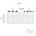
- FIG. 19 is a cross-sectional view of the antenna element 10j.
- FIG. 20 is a cross-sectional view of the antenna element 10j during manufacture.
- the antenna element 10j differs from the antenna element 10i in that reference conductor layers 25 and 27 are further provided.
- the reference conductor layers 25 and 27 are provided below the reference conductor layer 24 .
- the reference conductor layers 25 and 27 are exposed through the through hole H100.
- the plated layer 110 covers the inner peripheral surface of the through hole H100 and the reference conductor layers 25 and 27 exposed on the inner peripheral surface of the through hole H100.
- the through holes H100 are formed in the insulator layers 16a and 16b after the insulator layers 16a to 16f are stacked and pressure-bonded. Then, the plated layer 110 is formed on the inner peripheral surface of the through hole H100.
- Other structures of the antenna element 10j are the same as those of the antenna element 10i, so description thereof is omitted.
- the antenna element 10j can have the same effect as the antenna element 10i.
- FIG. 21 is a cross-sectional view of the antenna element 10k.
- the antenna element 10k differs from the antenna element 10 in that the second opening Op2 and the second insulating base non-formation area A2 do not exist.
- the rest of the structure of the antenna element 10k is the same as that of the antenna element 10, so the explanation is omitted.
- the antenna element 10k can have the same effect as the antenna element 10 does.
- FIG. 22 is a cross-sectional view of the antenna element 10l.
- the antenna element 10l differs from the antenna element 10a in that it further includes a first protective layer 70a and a second protective layer 70b.
- the first protective layer 70 a covers the upper main surface (first main surface) of the insulating base material 12 .
- the dielectric constant of the first protective layer 70 a is greater than that of the insulating base material 12 .
- the second protective layer 70 b covers the lower main surface (second main surface) of the insulating base material 12 .
- the dielectric constant of the second protective layer 70b is greater than that of the insulating base material 12 .
- Other structures of the antenna element 10d are the same as those of the antenna element 10a.
- the antenna element 10l can have the same effect as the antenna element 10a.
- the first protective layer 70 a covers the upper main surface (first main surface) of the insulating base material 12 . Therefore, the effect of shortening the wavelength of the high-frequency signal transmitted and received by the antenna conductor layer 20 is increased. Also, the antenna conductor layer 20 is protected by the first protective layer 70a. In addition, it is possible to simultaneously perform the filling of the material into the first insulating base non-formation region A1 and the second insulating base non-formation region A2 and the formation of the first protective layer 70a.
- FIG. 23 is a cross-sectional view of the antenna element 10m.
- the antenna element 10m is different from the antenna element 10l in that the first protective layer 70a is provided with a plurality of through holes h1 and the second protective layer 70b is provided with a plurality of through holes h2. differ from A through hole h1 is provided in a portion overlapping with one or more first openings Op1 and holes Sp0 in the first protective layer 70a when viewed in the vertical direction.
- the through hole h1 vertically penetrates the first protective layer 70a.
- the diameter of the through hole h1 is smaller than the diameter of the first opening Op1.
- Through holes h2 are provided in portions overlapping with the one or more second openings Op2 in the second protective layer 70b when viewed in the vertical direction.
- the diameter of the through hole h2 is smaller than the diameter of the second opening Op2.
- Other structures of the antenna element 10m are the same as those of the antenna element 10l.
- the antenna element 10m can have the same effect as the antenna element 10l.
- the through holes h1 are provided in the first protective layer 70a, the air in the first holes Sp1 can enter and exit. Therefore, even if the air inside the first holes Sp1 expands or contracts due to temperature changes such as reflow, the first protective layer 70 is less likely to peel off from the insulating base material 12 .
- FIG. 24 is a cross-sectional view of the antenna element 10n.
- the antenna element 10n differs from the antenna element 10k in that it further includes a first protective layer 70a.
- the first protective layer 70 a covers the upper main surface (first main surface) of the insulating base material 12 .
- the dielectric constant of the first protective layer 70 a is greater than that of the insulating base material 12 .
- the vertical thickness of the first protective layer 70a of the antenna element 10n is greater than the vertical thickness of the first protective layer 70a of the antenna element 10l.
- Other structures of antenna element 10n are the same as antenna element 10l.
- the antenna element 10n can have the same effect as the antenna element 10k.
- the first protective layer 70 a covers the upper main surface (first main surface) of the insulating base material 12 . Therefore, the effect of shortening the wavelength of the high-frequency signal transmitted and received by the antenna conductor layer 20 is increased. Also, the antenna conductor layer 20 is protected by the first protective layer 70a. In addition, it is possible to fill the insulating base non-formation region A0, the first insulating base non-formation region A1, and the second insulating base non-formation region A2 with the material and form the first protective layer 70a at the same time. .
- FIG. 25 is a cross-sectional view of the antenna element 10o.
- the antenna element 10o differs from the antenna element 10d in that the insulator layers 16a to 16e in the second section A22 are not removed.
- the rest of the structure of the antenna element 10o is the same as that of the antenna element 10d, so the description is omitted.
- the signal conductor layer 28 of the second section A22 is protected by the insulator layers 16a-16e.
- the resin etching of the second section A22 of the insulating base material 12 is not performed. The dry film is removed after resin etching.
- FIG. 26 is an exploded perspective view of the antenna element 10p.
- the antenna element 10p differs from the antenna element 10 in that the antenna conductor layers 20a and 20b are dipole antennas. Therefore, the antenna element 10h does not have the reference conductor layer 22.
- FIG. Each of the antenna conductor layers 20a and 20b is provided on the upper main surface of the insulator layer 16a.
- the antenna conductor layers 20a and 20b have a strip shape extending in the front-rear direction.
- a signal conductor layer 55a is connected to the antenna conductor layer 20a.
- a signal conductor layer 55b is connected to the antenna conductor layer 20b via an interlayer connection conductor v11.
- a plurality of first openings Op1 are provided in each of the antenna conductor layers 20a and 20b. Further, the insulator layer 16a is provided with a plurality of first insulating base non-formation regions A1. The rest of the structure of the antenna element 10p is the same as that of the antenna element 10, so the description is omitted. The antenna element 10p can have the same effect as the antenna element 10. FIG.
- circuit board 200 The circuit board 200 will be described below with reference to the drawings. 27 is a rear view of the circuit board 200. FIG.
- the circuit board 200 has a first section A111 and a second section A112.
- An antenna conductor layer 20 is provided in the first section A111. That is, the first section A111 has the same structure as the antenna elements 10, 10a-10h.
- the antenna conductor layer 20 is not provided in the second section A112. However, a signal conductor layer electrically connected to the antenna conductor layer 20 is provided.
- the first section A111 is not curved.
- the second section A112 is curved. However, the first section A111 may be curved. In this case, the radius of curvature of the first section A111 is greater than the radius of curvature of the second section A112.
- Holes Sp0a to Sp0f of antenna elements according to other modifications will be described below with reference to the drawings.
- 28 to 34 are cross-sectional views of holes Sp0a to Spg, respectively.
- the portion of the hole Sp0a having the maximum width in the direction perpendicular to the vertical direction may be located below the upper main surface of the insulator layer 16a.
- the air hole Sp0b may have a conical shape that is inverted upside down.
- the hole Sp0c may have a truncated cone shape that is inverted upside down.
- the holes Sp0d may be formed in a plurality of insulator layers 16a and 16b.
- the vacancies Sp0e may vertically penetrate between the upper main surface of the insulator layer 16a and the lower main surface of the insulator layer 16d.
- an insulator layer 116a may be provided between the insulator layers 16a and 16b.
- the material of the insulator layer 116a is, for example, fluororesin. Therefore, the insulator layer 116a is less likely to be removed by etching than the insulator layer 16a. Therefore, the vacancies Sp0f vertically penetrate only the insulator layer 16a.
- a through hole H120 may be formed in the insulator layer 116a. In this case, the vacancies Sp0g are formed in the insulator layers 16a and 16b.
- a conductor layer that is not etched may be provided instead of the insulator layer 116a in FIGS.
- the antenna elements according to the present invention are not limited to the antenna elements 10, 10a to 10p, and can be modified within the scope of the gist thereof.
- the configurations of the antenna elements 10, 10a to 10p may be combined arbitrarily.
- the holes Sp0, Sp0a to Sp0g may be formed by resin etching. In this case, processing of the insulator layers 16a and 16e is easy. Also, the holes Sp0, Sp0a to Sp0g may be formed by laser beam irradiation. In this case, the insulating layers 16a and 16e under the conductor layers can be scraped off by heat. Also, the holes Sp0, Sp0a to Sp0g may be formed by a combination of laser beam irradiation and resin etching. In this case, small diameter and deep holes can be formed.
- reference conductor layers 22, 24, and 26 are not essential components.
- the antenna conductor layer may be a dipole antenna or the like.
- the antenna conductor layer has a shape other than a rectangular shape, such as a linear shape.
- the antenna elements 10i to 10k may have a plurality of antenna conductor layers.
- At least a portion of the outer edge E1 of the antenna conductor should overlap the insulating base material non-formation area A0 when viewed in the vertical direction and should not be in contact with the insulating base material 12 .
- at least a portion of the inner edge E2 of the reference conductor layer 24 should overlap the insulating base non-formation region A0 when viewed in the vertical direction and should not be in contact with the insulating base 12 .
- An insulator layer may be further provided on the antenna conductor layer 20 .
- the material of this insulator layer may be the same material as the insulator layers 16a-16e. However, this insulator layer is not part of the insulating substrate 12 .
- the insulating base material 12 does not have to be flexible.
- the material of the insulating base material 12 may be a material other than a thermoplastic resin.
- the insulator layers 16a to 16f may be joined by an adhesive layer made of a material different from the material of the insulator layers 16a to 16f.
- a layer of the same material as the insulator layers 16a to 16d may be laminated on the upper main surface of the insulating base material 12. In this case, this layer is not part of the insulating substrate 12 . That is, the layers laminated above the upper main surface of the insulating base 12 on which the antenna conductor layer 20 is provided are not part of the insulating base 12 .
- the material filled in the first insulating base non-formation region A1 and the second insulating base non-formation region A2 is different from the material of the first protective layer 70a and the material of the second protective layer 70b. may be
Landscapes
- Details Of Aerials (AREA)
Priority Applications (3)
| Application Number | Priority Date | Filing Date | Title |
|---|---|---|---|
| JP2023518657A JP7652247B2 (ja) | 2021-05-07 | 2022-04-13 | アンテナ素子及び電子機器 |
| CN202290000397.2U CN220856914U (zh) | 2021-05-07 | 2022-04-13 | 天线元件以及电子设备 |
| US18/382,600 US12476354B2 (en) | 2021-05-07 | 2023-10-23 | Antenna element and electronic device |
Applications Claiming Priority (2)
| Application Number | Priority Date | Filing Date | Title |
|---|---|---|---|
| JP2021079045 | 2021-05-07 | ||
| JP2021-079045 | 2021-05-07 |
Related Child Applications (1)
| Application Number | Title | Priority Date | Filing Date |
|---|---|---|---|
| US18/382,600 Continuation US12476354B2 (en) | 2021-05-07 | 2023-10-23 | Antenna element and electronic device |
Publications (1)
| Publication Number | Publication Date |
|---|---|
| WO2022234769A1 true WO2022234769A1 (ja) | 2022-11-10 |
Family
ID=83932414
Family Applications (1)
| Application Number | Title | Priority Date | Filing Date |
|---|---|---|---|
| PCT/JP2022/017729 Ceased WO2022234769A1 (ja) | 2021-05-07 | 2022-04-13 | アンテナ素子及び電子機器 |
Country Status (4)
| Country | Link |
|---|---|
| US (1) | US12476354B2 (https=) |
| JP (1) | JP7652247B2 (https=) |
| CN (1) | CN220856914U (https=) |
| WO (1) | WO2022234769A1 (https=) |
Families Citing this family (1)
| Publication number | Priority date | Publication date | Assignee | Title |
|---|---|---|---|---|
| KR102743721B1 (ko) * | 2019-11-08 | 2024-12-17 | 삼성전자주식회사 | 송신 안테나 선택 방법 및 전자 장치 |
Citations (10)
| Publication number | Priority date | Publication date | Assignee | Title |
|---|---|---|---|---|
| JPH03192804A (ja) * | 1989-12-22 | 1991-08-22 | Nippon Telegr & Teleph Corp <Ntt> | アンテナ装置 |
| JPH10190351A (ja) * | 1996-12-25 | 1998-07-21 | Mitsubishi Electric Corp | ミリ波帯平面アンテナ |
| JPH11122032A (ja) * | 1997-10-11 | 1999-04-30 | Yokowo Co Ltd | マイクロストリップアンテナ |
| JP2002118417A (ja) * | 2000-10-10 | 2002-04-19 | Alps Electric Co Ltd | 平面パッチアンテナ |
| JP2002217637A (ja) * | 2001-01-15 | 2002-08-02 | Yokowo Co Ltd | 内蔵アンテナ |
| JP2006064679A (ja) * | 2004-08-30 | 2006-03-09 | Canon Inc | アンテナを備える電磁波素子 |
| EP1793451A1 (en) * | 2005-12-02 | 2007-06-06 | M/A-Com, Inc. | Compact broadband patch antenna |
| JP2013214939A (ja) * | 2012-03-08 | 2013-10-17 | Canon Inc | 電磁波を放射または受信する装置 |
| WO2017168705A1 (ja) * | 2016-03-31 | 2017-10-05 | 日本電業工作株式会社 | アンテナ |
| JP2018137737A (ja) * | 2017-02-21 | 2018-08-30 | 京セラ株式会社 | アンテナ基板 |
Family Cites Families (14)
| Publication number | Priority date | Publication date | Assignee | Title |
|---|---|---|---|---|
| JPH05175719A (ja) | 1991-12-20 | 1993-07-13 | Toko Inc | マイクロストリップアンテナの製造方法および共振周波数調整方法 |
| JPH1065437A (ja) | 1996-08-21 | 1998-03-06 | Saitama Nippon Denki Kk | 板状逆fアンテナおよび無線装置 |
| JP2004096259A (ja) | 2002-08-30 | 2004-03-25 | Matsushita Electric Ind Co Ltd | 多周波マイクロストリップアンテナ |
| JP4181083B2 (ja) | 2003-12-24 | 2008-11-12 | 三菱電機株式会社 | めっき方法と高周波線路 |
| US7812767B2 (en) * | 2004-09-07 | 2010-10-12 | Nippon Telegraph And Telephone Corporation | Antenna device, array antenna device using the antenna device, module, module array and package module |
| US7466269B2 (en) * | 2006-05-24 | 2008-12-16 | Wavebender, Inc. | Variable dielectric constant-based antenna and array |
| CN101652897B (zh) | 2007-04-05 | 2013-07-31 | 艾利森电话股份有限公司 | 极化相关的波束宽度调整器 |
| JP5983760B2 (ja) * | 2012-11-07 | 2016-09-06 | 株式会社村田製作所 | アレーアンテナ |
| WO2015133454A1 (ja) * | 2014-03-03 | 2015-09-11 | 株式会社フジクラ | アンテナモジュール、及び、その実装方法 |
| US9876278B2 (en) * | 2015-04-21 | 2018-01-23 | Kyocera Corporation | Antenna board |
| JP6687469B2 (ja) * | 2016-06-14 | 2020-04-22 | 日立オートモティブシステムズ株式会社 | ミリ波帯通信装置 |
| EP3698436B1 (en) * | 2017-10-18 | 2022-02-23 | CommScope Technologies LLC | Broadband stacked patch radiating elements and related phased array antennas |
| US12126100B2 (en) * | 2020-09-29 | 2024-10-22 | The Regents Of The University Of California | Apparatus for electromagnetic wave manipulation |
| TWI749987B (zh) * | 2021-01-05 | 2021-12-11 | 友達光電股份有限公司 | 天線結構及陣列天線模組 |
-
2022
- 2022-04-13 WO PCT/JP2022/017729 patent/WO2022234769A1/ja not_active Ceased
- 2022-04-13 CN CN202290000397.2U patent/CN220856914U/zh active Active
- 2022-04-13 JP JP2023518657A patent/JP7652247B2/ja active Active
-
2023
- 2023-10-23 US US18/382,600 patent/US12476354B2/en active Active
Patent Citations (10)
| Publication number | Priority date | Publication date | Assignee | Title |
|---|---|---|---|---|
| JPH03192804A (ja) * | 1989-12-22 | 1991-08-22 | Nippon Telegr & Teleph Corp <Ntt> | アンテナ装置 |
| JPH10190351A (ja) * | 1996-12-25 | 1998-07-21 | Mitsubishi Electric Corp | ミリ波帯平面アンテナ |
| JPH11122032A (ja) * | 1997-10-11 | 1999-04-30 | Yokowo Co Ltd | マイクロストリップアンテナ |
| JP2002118417A (ja) * | 2000-10-10 | 2002-04-19 | Alps Electric Co Ltd | 平面パッチアンテナ |
| JP2002217637A (ja) * | 2001-01-15 | 2002-08-02 | Yokowo Co Ltd | 内蔵アンテナ |
| JP2006064679A (ja) * | 2004-08-30 | 2006-03-09 | Canon Inc | アンテナを備える電磁波素子 |
| EP1793451A1 (en) * | 2005-12-02 | 2007-06-06 | M/A-Com, Inc. | Compact broadband patch antenna |
| JP2013214939A (ja) * | 2012-03-08 | 2013-10-17 | Canon Inc | 電磁波を放射または受信する装置 |
| WO2017168705A1 (ja) * | 2016-03-31 | 2017-10-05 | 日本電業工作株式会社 | アンテナ |
| JP2018137737A (ja) * | 2017-02-21 | 2018-08-30 | 京セラ株式会社 | アンテナ基板 |
Also Published As
| Publication number | Publication date |
|---|---|
| JP7652247B2 (ja) | 2025-03-27 |
| JPWO2022234769A1 (https=) | 2022-11-10 |
| US20240055754A1 (en) | 2024-02-15 |
| US12476354B2 (en) | 2025-11-18 |
| CN220856914U (zh) | 2024-04-26 |
Similar Documents
| Publication | Publication Date | Title |
|---|---|---|
| US11081804B2 (en) | Antenna-integrated type communication module and manufacturing method for the same | |
| CN104037166B (zh) | 包含天线层的半导体封装件及其制造方法 | |
| US7675466B2 (en) | Antenna array feed line structures for millimeter wave applications | |
| US7236070B2 (en) | Electronic component module and manufacturing method thereof | |
| JP5669043B2 (ja) | ポスト壁導波路アンテナ及びアンテナモジュール | |
| KR20200120580A (ko) | 칩 안테나 모듈 및 이를 포함하는 전자기기 | |
| CN110739528B (zh) | 天线设备 | |
| KR20210023958A (ko) | 칩 안테나 모듈 | |
| US9705194B2 (en) | Antenna module | |
| JP7136302B2 (ja) | 基板 | |
| US20180316080A1 (en) | High-frequency signal transmission line and electronic device | |
| JP5081985B2 (ja) | ケーブルコネクタおよびアンテナ部品 | |
| US11018434B2 (en) | Antenna apparatus, and manufacturing method | |
| US12494565B2 (en) | Coupling structure and antenna module | |
| JP5472552B2 (ja) | 高周波信号線路及び電子機器 | |
| KR102222943B1 (ko) | 칩 안테나 모듈 | |
| WO2022234769A1 (ja) | アンテナ素子及び電子機器 | |
| JP7420315B2 (ja) | アンテナ素子、電子機器及びアンテナ素子の製造方法 | |
| JP6569826B2 (ja) | アンテナモジュール | |
| JP2019186741A (ja) | アンテナ及びアンテナモジュール | |
| JP7803439B2 (ja) | 多層基板 | |
| JP7794328B2 (ja) | 多層基板 | |
| CN103985955A (zh) | 无线通信装置的双频天线 | |
| CN118040274A (zh) | 一种互联装置及无线通信装置 |
Legal Events
| Date | Code | Title | Description |
|---|---|---|---|
| 121 | Ep: the epo has been informed by wipo that ep was designated in this application |
Ref document number: 22798876 Country of ref document: EP Kind code of ref document: A1 |
|
| WWE | Wipo information: entry into national phase |
Ref document number: 2023518657 Country of ref document: JP |
|
| WWE | Wipo information: entry into national phase |
Ref document number: 202290000397.2 Country of ref document: CN |
|
| NENP | Non-entry into the national phase |
Ref country code: DE |
|
| 122 | Ep: pct application non-entry in european phase |
Ref document number: 22798876 Country of ref document: EP Kind code of ref document: A1 |