WO2022234769A1 - Antenna element and electronic device - Google Patents
Antenna element and electronic device Download PDFInfo
- Publication number
- WO2022234769A1 WO2022234769A1 PCT/JP2022/017729 JP2022017729W WO2022234769A1 WO 2022234769 A1 WO2022234769 A1 WO 2022234769A1 JP 2022017729 W JP2022017729 W JP 2022017729W WO 2022234769 A1 WO2022234769 A1 WO 2022234769A1
- Authority
- WO
- WIPO (PCT)
- Prior art keywords
- antenna element
- insulating base
- antenna
- conductor layer
- vertical direction
- Prior art date
Links
- 239000004020 conductor Substances 0.000 claims abstract description 300
- 239000000463 material Substances 0.000 claims abstract description 116
- 239000010410 layer Substances 0.000 claims description 332
- 230000015572 biosynthetic process Effects 0.000 claims description 64
- 239000011241 protective layer Substances 0.000 claims description 39
- 239000000758 substrate Substances 0.000 claims description 10
- 229920005992 thermoplastic resin Polymers 0.000 claims description 7
- 239000012212 insulator Substances 0.000 abstract description 79
- 230000004048 modification Effects 0.000 description 30
- 238000012986 modification Methods 0.000 description 30
- 239000011229 interlayer Substances 0.000 description 27
- 230000000694 effects Effects 0.000 description 19
- 238000004519 manufacturing process Methods 0.000 description 12
- 230000005855 radiation Effects 0.000 description 12
- 238000005530 etching Methods 0.000 description 11
- 230000005684 electric field Effects 0.000 description 7
- 230000006866 deterioration Effects 0.000 description 5
- 239000011888 foil Substances 0.000 description 5
- 239000002184 metal Substances 0.000 description 5
- 229910052751 metal Inorganic materials 0.000 description 5
- 229920005989 resin Polymers 0.000 description 5
- 239000011347 resin Substances 0.000 description 5
- 230000002093 peripheral effect Effects 0.000 description 4
- 230000008878 coupling Effects 0.000 description 3
- 238000010168 coupling process Methods 0.000 description 3
- 238000005859 coupling reaction Methods 0.000 description 3
- 239000011159 matrix material Substances 0.000 description 3
- 238000000034 method Methods 0.000 description 3
- 238000004904 shortening Methods 0.000 description 3
- 239000012790 adhesive layer Substances 0.000 description 2
- 238000002788 crimping Methods 0.000 description 2
- 230000005489 elastic deformation Effects 0.000 description 2
- 238000010438 heat treatment Methods 0.000 description 2
- 239000004033 plastic Substances 0.000 description 2
- 229920001343 polytetrafluoroethylene Polymers 0.000 description 2
- 239000004810 polytetrafluoroethylene Substances 0.000 description 2
- RYGMFSIKBFXOCR-UHFFFAOYSA-N Copper Chemical compound [Cu] RYGMFSIKBFXOCR-UHFFFAOYSA-N 0.000 description 1
- 229920000106 Liquid crystal polymer Polymers 0.000 description 1
- 239000004977 Liquid-crystal polymers (LCPs) Substances 0.000 description 1
- 239000004642 Polyimide Substances 0.000 description 1
- 239000000919 ceramic Substances 0.000 description 1
- 238000004891 communication Methods 0.000 description 1
- 239000011889 copper foil Substances 0.000 description 1
- 238000005304 joining Methods 0.000 description 1
- 230000000149 penetrating effect Effects 0.000 description 1
- 238000007747 plating Methods 0.000 description 1
- 229920001721 polyimide Polymers 0.000 description 1
- -1 polytetrafluoroethylene Polymers 0.000 description 1
- 239000000843 powder Substances 0.000 description 1
Images


Classifications
-
- H—ELECTRICITY
- H01—ELECTRIC ELEMENTS
- H01Q—ANTENNAS, i.e. RADIO AERIALS
- H01Q13/00—Waveguide horns or mouths; Slot antennas; Leaky-waveguide antennas; Equivalent structures causing radiation along the transmission path of a guided wave
- H01Q13/10—Resonant slot antennas
- H01Q13/106—Microstrip slot antennas
-
- H—ELECTRICITY
- H01—ELECTRIC ELEMENTS
- H01Q—ANTENNAS, i.e. RADIO AERIALS
- H01Q1/00—Details of, or arrangements associated with, antennas
- H01Q1/36—Structural form of radiating elements, e.g. cone, spiral, umbrella; Particular materials used therewith
- H01Q1/38—Structural form of radiating elements, e.g. cone, spiral, umbrella; Particular materials used therewith formed by a conductive layer on an insulating support
-
- H—ELECTRICITY
- H01—ELECTRIC ELEMENTS
- H01Q—ANTENNAS, i.e. RADIO AERIALS
- H01Q1/00—Details of, or arrangements associated with, antennas
- H01Q1/40—Radiating elements coated with or embedded in protective material
Definitions
- the present invention relates to an antenna element provided with an antenna conductor layer.
- the microstrip antenna described in Patent Document 1 As an invention related to conventional antenna elements, for example, the microstrip antenna described in Patent Document 1 is known.
- This microstrip antenna comprises a dielectric substrate, a rectangular conductor and a ground conductor.
- the dielectric substrate has an upper major surface and a lower major surface.
- a rectangular conductor is provided on the upper main surface of the dielectric substrate.
- a ground conductor is provided on the lower main surface of the dielectric substrate.
- the rectangular conductor overlaps the ground conductor when viewed in the vertical direction.
- a rectangular conductor functions as an antenna.
- electric field concentration may occur at the outer edge of the rectangular conductor when viewed in the vertical direction.
- electric field concentration occurs, for example, electric field coupling between the conductors existing around the rectangular conductor and the rectangular conductor is likely to occur.
- electromagnetic waves are likely to be radiated from the rectangular conductor toward conductors present around the rectangular conductor.
- the radiation efficiency of the microstrip antenna is reduced.
- an object of the present invention is to provide an antenna element and an electronic device capable of suppressing a decrease in the radiation efficiency of the antenna element.
- An antenna element includes: An antenna element, an insulating base material having a first principal surface and a second principal surface aligned in the vertical direction; one or more antenna conductor layers provided on the first main surface of the insulating base; and an insulating base non-formed region is positioned between the insulating base and the antenna conductor layer in the vertical direction;
- the insulating base does not exist in the insulating base non-formation region, at least a portion of the outer edge of the one or more antenna conductors overlaps the insulating base non-formed region when viewed in the vertical direction and is not in contact with the insulating base;
- the antenna element has the structure (A) or (B), and (A) the one or more insulating base non-forming regions are voids, and (B) the one or more insulating bases.
- a low dielectric constant material having a dielectric constant lower than that of the insulating substrate is provided in the non-forming region.
- the antenna element and the electronic device according to the present invention it is possible to suppress the deterioration of the radiation efficiency of the antenna element.
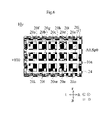
- FIG. 1 is an exploded perspective view of the antenna element 10.
- FIG. FIG. 2 is a cross-sectional view along AA in FIG.
- FIG. 3 is a flow chart showing the manufacturing process of the antenna element 10.
- FIG. 4 is a cross-sectional view of the antenna element 10a.
- FIG. 5 is a top view of the insulator layer 16a of the antenna element 10b.
- FIG. 6 is a top view of the insulator layer 16a of the antenna element 10c.
- FIG. 7 is a cross-sectional view of the antenna element 10c.
- FIG. 8 is a top view of the insulator layer 16a of the antenna element 10d.
- FIG. 9 is a cross-sectional view of the antenna element 10d.
- FIG. 10 is a cross-sectional view of the antenna element 10d.
- FIG. 11 is a cross-sectional view of the antenna element 10e.
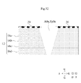
- FIG. 12 is a cross-sectional view of the antenna element 10f.
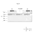
- FIG. 13 is a top view of the insulator layer 16a of the antenna element 10g.
- FIG. 14 is a cross-sectional view of the antenna element 10g.
- FIG. 15 is a cross-sectional view of the antenna element 10h.
- FIG. 16 is a cross-sectional view of the antenna element 10i.
- FIG. 17 is a top view of the antenna element 10i.
- FIG. 18 is a cross-sectional view of the antenna element 10i during manufacture.
- FIG. 19 is a cross-sectional view of the antenna element 10j.
- FIG. 11 is a cross-sectional view of the antenna element 10e.
- FIG. 12 is a cross-sectional view of the antenna element 10f.
- FIG. 13 is a top view of the
- FIG. 20 is a cross-sectional view of the antenna element 10j during manufacture.
- FIG. 21 is a cross-sectional view of the antenna element 10k.
- FIG. 22 is a cross-sectional view of the antenna element 10l.
- FIG. 23 is a cross-sectional view of the antenna element 10m.
- FIG. 24 is a cross-sectional view of the antenna element 10n.
- FIG. 25 is a cross-sectional view of the antenna element 10o.
- FIG. 26 is an exploded perspective view of the antenna element 10p.
- 27 is a rear view of the circuit board 200.
- FIG. FIG. 28 is a cross-sectional view of the hole Sp0a.
- FIG. 29 is a cross-sectional view of the hole Sp0b.
- FIG. 30 is a cross-sectional view of the hole Sp0c.
- FIG. 31 is a cross-sectional view of the hole Sp0d.
- FIG. 32 is a cross-sectional view of the hole Sp0e.
- FIG. 33 is a cross-sectional view of the hole Sp0f.
- FIG. 34 is a cross-sectional view of the hole Sp0g.
- FIG. 1 is an exploded perspective view of the antenna element 10.
- FIG. 1 is an exploded perspective view of the antenna element 10.
- FIG. 2 is a cross-sectional view of the electronic device 1 including the antenna element 10. As shown in FIG. FIG. 2 is a cross-sectional view along AA in FIG. However, FIG. 2 shows the housing 100 that is not shown in FIG.
- the vertical direction is defined as the direction in which the normal lines of the upper and lower main surfaces of the insulating base material 12 of the antenna element 10 extend.
- the vertical direction coincides with the stacking direction of the insulating base material 12 .
- the direction in which the long side of the antenna conductor layer 20 of the antenna element 10 extends is defined as the horizontal direction.
- the direction in which the short side of the antenna conductor layer 20 of the antenna element 10 extends is defined as the front-rear direction.
- the up-down direction is perpendicular to the front-rear direction.
- the left-right direction is orthogonal to the up-down direction and the front-rear direction.
- X is a part or member of the antenna element 10.
- each part of X is defined as follows.
- front of X is meant the front half of X.
- Back of X means the back half of X.
- the left part of X means the left half of X.
- the right part of X means the right half of X.
- Top of X means the top half of X.
- the lower part of X means the lower half of X.
- the leading edge of X means the leading edge of X.
- the trailing end of X means the trailing end of X.
- the left end of X means the end of X in the left direction.
- the right end of X means the end of X in the right direction.
- the upper end of X means the end of X in the upward direction.
- the lower end of X means the lower end of X.
- the front end of X means the front end of X and its vicinity.
- the rear end of X means the rear end of X and its vicinity.
- the left end of X means the left end of X and its vicinity.
- the right end of X means the right end of X and its vicinity.
- the upper end of X means the upper end of X and its vicinity.
- the lower end of X means the lower end of X and its vicinity.
- the antenna element 10 includes an insulating base material 12, an antenna conductor layer 20, reference conductor layers 22, 24 and 26, a signal conductor layer 28, a plurality of interlayer connection conductors v1 and interlayer connection conductors v2. there is
- the insulating base material 12 has a plate shape. Therefore, the insulating base material 12 has an upper principal surface (first principal surface) and a lower principal surface (second principal surface) which are aligned in the vertical direction.
- the upper main surface and the lower main surface of the insulating base material 12 have a rectangular shape with long sides extending in the left-right direction. Therefore, the length of the insulating base material 12 in the left-right direction is longer than the length of the insulating base material 12 in the front-rear direction.
- the insulating base material 12 includes insulator layers 16a to 16e, as shown in FIG.
- the insulating base material 12 has a structure in which insulating layers 16a to 16e are stacked vertically.
- the insulator layers 16a-16e are arranged in this order from top to bottom.
- the insulator layers 16a to 16e have the same rectangular shape as the insulating base material 12 when viewed in the vertical direction.
- the insulator layers 16a-16e are flexible dielectric sheets.
- the material of the insulating base material 12 is, for example, a thermoplastic resin.
- Thermoplastic resins are, for example, thermoplastic resins such as liquid crystal polymer and PTFE (polytetrafluoroethylene).
- the material of the insulating base material 12 may be polyimide.
- the insulating base material 12 has flexibility. Therefore, the antenna element 10 may be used while being bent. “The antenna element 10 is bent” means that the antenna element 10 is deformed and bent by applying an external force to the antenna element 10 .
- the deformation may be elastic deformation, plastic deformation, or both elastic deformation and plastic deformation.
- the antenna conductor layer 20 is provided on the upper main surface or the lower main surface of the insulating base material 12 .
- the antenna conductor layer 20 is provided on the upper main surface of the insulating base material 12 .
- the antenna conductor layer 20 is provided on the upper main surface of the insulator layer 16a (first insulator layer).
- the antenna conductor layer 20 has a rectangular shape with long sides extending in the horizontal direction when viewed in the vertical direction.
- the antenna conductor layer 20 resonates on both the short side extending in the front-rear direction and the long side extending in the left-right direction.
- the short side extending in the front-rear direction and the long side extending in the left-right direction of the antenna conductor layer 20 are about half the wavelength of the high-frequency signal transmitted and received by the antenna conductor layer 20 .
- the length of the wavelength of the high-frequency signal transmitted and received by the antenna conductor layer 20 is the wavelength in consideration of the wavelength shortening effect due to the dielectric constant of the insulating base material 12 .
- the antenna conductor layer 20 radiates high frequency signals as electromagnetic waves. Further, the antenna conductor layer 20 receives high-frequency signals of electromagnetic waves.
- the signal conductor layer 28 is provided on the insulating base material 12 .
- the signal conductor layer 28 is provided on the upper main surface of the insulator layer 16c.
- the signal conductor layer 28 has a linear shape extending in the left-right direction. The right end portion of the signal conductor layer 28 overlaps the antenna conductor layer 20 when viewed in the vertical direction.
- the signal conductor layer 28 transmits high frequency signals.
- the interlayer connection conductor v2 electrically connects the antenna conductor layer 20 and the signal conductor layer . More specifically, the interlayer connection conductor v2 penetrates the insulator layers 16a and 16b in the vertical direction. An upper end of the interlayer connection conductor v2 is connected to the antenna conductor layer 20 . The position where the interlayer connection conductor v2 is connected in the antenna conductor layer 20 is a feeding point for high frequency signals. The lower end of the interlayer connection conductor v2 is connected to the right end of the signal conductor layer 28 .
- the reference conductor layer 22 is provided on the insulating base material 12 and below the antenna conductor layer 20 .
- the reference conductor layer 22 is provided on the lower main surface of the insulator layer 16e.
- the reference conductor layer 22 overlaps the antenna conductor layer 20 when viewed in the vertical direction.
- the reference conductor layer 22 has a rectangular shape with long sides extending in the horizontal direction when viewed in the vertical direction.
- the reference conductor layer 22 protrudes from the antenna conductor layer 20 in the front-rear direction and the left-right direction when viewed in the vertical direction. That is, the outer edge of the reference conductor layer 22 includes the outer edge of the antenna conductor layer 20 when viewed in the vertical direction.
- the reference conductor layer 24 is provided on the insulating base material 12 .
- the reference conductor layer 24 is provided on the upper main surface of the insulating base 12 when the antenna conductor layer 20 is provided on the upper main surface of the insulating base 12 .
- the reference conductor layer 24 is provided on the upper main surface of the insulating base material 12 .
- the reference conductor layer 24 is provided on the upper main surface of the insulator layer 16a on which the antenna conductor layer 20 is provided.
- the reference conductor layer 24 has a rectangular frame shape when viewed in the vertical direction.
- the reference conductor layer 24 surrounds the antenna conductor layer 20 when viewed in the vertical direction.
- the antenna conductor layer 20 and the reference conductor layer 24 are separated from each other so that the antenna conductor layer 20 and the reference conductor layer 24 are not short-circuited.
- the reference conductor layer 26 is provided on the insulating base material 12 .
- the reference conductor layer 26 is provided on the upper main surface of the insulator layer 16c.
- the shape of the reference conductor layer 26 is substantially the same as that of the reference conductor layer 24 .
- the reference conductor layer 26 is not in contact with the signal conductor layer 28 so that the reference conductor layer 26 and the signal conductor layer 28 are not short-circuited.
- a plurality of interlayer connection conductors v1 electrically connect the reference conductor layer 22, the reference conductor layer 24, and the reference conductor layer . More specifically, the plurality of interlayer connection conductors v1 vertically penetrate through the insulator layers 16a to 16e. Upper ends of the plurality of interlayer connection conductors v1 are connected to the reference conductor layer 24 . Middle portions of the plurality of interlayer connection conductors v1 are connected to the reference conductor layer 26 . Lower ends of the plurality of interlayer connection conductors v1 are connected to the reference conductor layer 22 .
- the plurality of interlayer connection conductors v1 are arranged along the reference conductor layer 24 when viewed in the vertical direction. That is, the plurality of interlayer connection conductors v1 are arranged so as to surround the antenna conductor layer 20 when viewed in the vertical direction.
- the antenna conductor layer 20, the reference conductor layers 22, 24, 26, and the signal conductor layer 28 as described above are formed by, for example, etching a metal foil provided on the upper or lower main surface of the insulator layers 16a to 16e. It is formed by being The metal foil is, for example, copper foil.
- the interlayer connection conductors v1 and v2 are, for example, via-hole conductors.
- the via-hole conductors are produced by forming through-holes in the insulating layers 16a to 16e, filling the through-holes with a conductive paste, and solidifying the conductive paste by heating.
- the interlayer connection conductors v1 and v2 may be, for example, through-hole conductors. Through-hole conductors are produced by forming through-holes penetrating all or part of the insulator layers 16a to 16e and plating the through-holes.
- the insulating base material non-formation region A0 and the holes Sp0 will be described.
- the insulating base material non-forming area A0 is formed by partially recessing the upper main surface of the insulating base material 12 downward.
- the insulating base non-formation region A0 is positioned between the insulating base 12 and the antenna conductor layer 20 in the vertical direction. That is, the plurality of insulating base non-formation regions A0 are provided between the insulator layer 16a and the antenna conductor layer 20 in the vertical direction.
- the insulating base non-formation region A0 is positioned below the antenna conductor layer 20 and the reference conductor layer 24.
- the insulating base material 12 does not exist in the insulating base material non-formation area A0.
- the insulating base non-formation region A0 is the vacancy Sp0.
- the outer edge E1 of the antenna conductor layer 20 means an edge positioned outside the antenna conductor layer 20 when viewed in the vertical direction.
- the antenna conductor layer 20 does not exist outside the outer edge E1 of the antenna conductor layer 20 .
- the outer edge E1 has a rectangular shape.
- the inner edge E2 of the reference conductor layer 24 means an edge located inside the reference conductor layer 24 when viewed in the vertical direction.
- the inner edge E2 of the reference conductor layer 24 is positioned within the area surrounded by the outer edge of the reference conductor layer 24 .
- the reference conductor layer 24 exists outside the inner edge E2 of the reference conductor layer 24 .
- the inner edge E2 has a rectangular shape.
- the inner edge E2 surrounds the outer edge E1 when viewed in the vertical direction. Also, the distance between the inner edge E2 and the outer edge E1 is constant.
- a conductor non-formation area A11 is formed between the outer edge E1 of the antenna conductor layer 20 and the inner edge E2 of the reference conductor layer 24 .
- the conductor non-formation area A11 is an area in which no conductor exists.
- the conductor non-formation area A11 has a rectangular frame shape when viewed in the vertical direction.
- the insulating base non-formation region A0 and the holes Sp0 are along the outer edge E1 of the antenna conductor layer 20 and the inner edge E2 of the reference conductor layer 24 when viewed in the vertical direction. That is, the insulating base non-formation region A0 and the holes Sp0 overlap the conductor non-formation region A11 when viewed in the vertical direction. Therefore, the insulating base material non-formation region A0 and the holes Sp0 have a rectangular frame shape when viewed in the vertical direction. Thus, the insulating base non-formation region A0 and the holes Sp0 surround the antenna conductor layer 20 when viewed in the vertical direction. In addition, the reference conductor layer 24 surrounds the insulating base non-formed region A0 and the holes Sp0 when viewed in the vertical direction.
- the insulating base non-formation region A0 and the inner edge P1 of the hole Sp0 overlap the antenna conductor layer 20 when viewed in the vertical direction.
- a hole Sp0 exists between the outer edge E1 of the antenna conductor layer 20 and the insulating base material 12.
- the entire outer edge E ⁇ b>1 of the antenna conductor overlaps the insulating base material non-formation region A ⁇ b>0 when viewed in the vertical direction and is not in contact with the insulating base material 12 .
- the outer edges P2 of the insulating base non-formation region A0 and the holes Sp0 overlap the reference conductor layer 24 when viewed in the vertical direction.
- a hole Sp0 exists between the inner edge E2 of the reference conductor layer 24 and the insulating base material 12.
- the entire inner edge E2 of the reference conductor layer 24 overlaps the insulating base non-formed region A0 when viewed in the vertical direction, and is not in contact with the insulating base 12 .
- a plurality of first openings Op1 are provided in the antenna conductor layer 20 .
- the plurality of first openings Op1 are arranged in a matrix when viewed in the vertical direction.
- the multiple first openings Op1 have annular outer edges when viewed in the vertical direction.
- the plurality of first openings Op1 have circular outer edges when viewed in the vertical direction.
- an annular shape is not limited to a circular ring, and includes a rectangular shape and a triangular shape.
- the annular outer rim has no edges. Therefore, the first opening Op1 does not include a notch.
- the outer edge of the notch has edges.
- the outer edge of the notch is a part of the outer edge of the antenna conductor layer 20 that is bent toward the center of the antenna conductor layer 20 . Therefore, the outer edge of the notch is part of the antenna conductor layer 20 .
- the antenna conductor layer 20 does not exist within the first opening Op1.
- the interval between the plurality of adjacent first openings Op1 is, for example, 1/4 or less of the length of the wavelength of the high-frequency signal transmitted and received by the antenna conductor layer 20 .
- a plurality of first insulating base non-formation regions A1 are provided on the insulating base 12 .
- the plurality of first insulating base non-formation regions A1 are provided in the insulator layer 16a.
- the plurality of first insulating base non-formation regions A1 are positioned below the antenna conductor layer 20 .
- the insulating base material 12 does not exist in the plurality of first insulating base non-formed regions A1.
- the plurality of first insulating base non-formation regions A1 are the first holes Sp1.
- the plurality of first insulating base non-formation regions A1 are arranged in a matrix when viewed in the vertical direction so as to correspond to the plurality of first openings Op1.
- the plurality of first insulating base non-formation regions A1 have annular outer edges when viewed in the vertical direction.
- the plurality of first insulating base non-formation regions A1 have circular outer edges when viewed in the vertical direction.
- each of the plurality of first insulating base non-formation regions A1 includes each of the plurality of first openings Op1 when viewed in the vertical direction. That is, each of the plurality of first openings Op1 does not protrude from the plurality of first insulating base non-formation regions A1. Therefore, the diameter of the first insulating base non-formation region A1 is larger than the diameter of the first opening Op1.
- the first insulating base non-formation region A1 has a hemispherical shape.
- the plurality of second openings Op2, the plurality of second insulating base non-formation regions A2, and the plurality of second holes Sp2 will be described.
- the plurality of second openings Op2, the plurality of second insulating base non-forming regions A2, and the plurality of second holes Sp2 are formed by the plurality of first openings Op1, the plurality of first insulating base non-forming regions A1, and the plurality of second openings Op2. It has a vertically symmetrical structure with one vacancy Sp1. Therefore, description of the plurality of second openings Op2, the plurality of second insulating base non-formation regions A2, and the plurality of second holes Sp2 will be omitted.
- the electronic device 1 includes an antenna element 10 and a housing 100, as shown in FIG. Antenna element 10 is housed in housing 100 .
- the electronic device 1 is, for example, a mobile wireless communication terminal such as a smart phone.
- FIG. 3 is a flow chart showing the manufacturing process of the antenna element 10. As shown in FIG.
- insulator layers 16a to 16c with metal foil attached to the upper main surface are prepared.
- insulator layers 16d and 16e having metal foil attached to their lower main surfaces are prepared (step S1).
- a mask is formed on the metal foil and etching is performed to form the antenna conductor layer 20, the reference conductor layers 22, 24 and 26 and the signal conductor layer 28 on the insulator layers 16a to 16e (step S2). .
- a plurality of interlayer connection conductors v1 and interlayer connection conductors v2 are formed on the insulator layers 16a to 16e (step S3). Specifically, the insulator layers 16a to 16e are irradiated with a laser beam to form a plurality of through holes. After that, the plurality of through holes are filled with a conductive paste.
- the insulating base material 12 is formed by crimping the insulator layers 16a to 16e (step S4, crimping step).
- the insulator layers 16a to 16e are heated while being pressed vertically.
- the insulator layers 16a to 16e are softened, and the insulator layers 16a to 16e are integrated.
- the conductive paste is solidified by heating to form a plurality of interlayer connection conductors v1 and interlayer connection conductors v2.
- vacancies Sp0, a plurality of first vacancies Sp1, and a plurality of second vacancies Sp2 are formed in the insulator layers 16a and 16e (step S5). Specifically, by etching the insulator layer 16a using the antenna conductor layer 20 as a mask, the holes Sp0 and the plurality of first holes Sp1 are formed (first hole forming step). Furthermore, by etching the insulator layer 16e using the reference conductor layer 22 as a mask, a plurality of second holes Sp2 are formed (second hole forming step). Through the above steps, the antenna element 10 is completed.
- the outer edge E ⁇ b>1 of the antenna conductor layer 20 overlaps the insulating base material non-formed area A ⁇ b>0 when viewed in the vertical direction and is not in contact with the insulating base material 12 .
- the insulating base non-formation region A0 is the hole Sp0.
- the dielectric constant around the outer edge E1 of the antenna conductor layer 20 is lowered. Therefore, the occurrence of electric field concentration at the outer edge E1 of the antenna conductor layer 20 is suppressed.
- electric field coupling between the antenna conductor layer 20 and the reference conductor layer 24 is suppressed.
- the radiation of electromagnetic waves from the antenna conductor layer 20 toward the reference conductor layer 24 is suppressed, and the deterioration of the radiation efficiency of the microstrip antenna is suppressed.
- the deterioration of the radiation efficiency of the antenna element 10 can be suppressed also for the following reasons.
- the inner edge E2 of the reference conductor layer 24 overlaps the insulating base non-formed region A0 when viewed in the vertical direction, and is not in contact with the insulating base 12 .
- the insulating base non-formation region A0 is the hole Sp0.
- the dielectric constant around the inner edge E2 of the reference conductor layer 24 is lowered. Therefore, the occurrence of electric field concentration at the inner edge E2 of the reference conductor layer 24 is suppressed.
- electric field coupling between the antenna conductor layer 20 and the reference conductor layer 24 is suppressed.
- the radiation of electromagnetic waves from the antenna conductor layer 20 toward the reference conductor layer 24 is suppressed, and the deterioration of the radiation efficiency of the microstrip antenna is suppressed.
- each of the plurality of first insulating base non-formation regions A1 is located below the antenna conductor layer 20 .
- Each of the plurality of second insulating base non-formation regions A2 is located on the reference conductor layer 22 .
- the plurality of first insulating base non-formation regions A1 and the plurality of second insulating base non-formation regions A2 are first holes Sp1 and second holes Sp2, respectively. This reduces the dielectric constant of the region between the antenna conductor layer 20 and the reference conductor layer 22 . Therefore, the distance between the antenna conductor layer 20 and the reference conductor layer 22 can be shortened in order to form the designed capacitance between the antenna conductor layer 20 and the reference conductor layer 22 . As a result, the thickness of the antenna element 10 can be reduced.
- the antenna element 10 can be easily bent. More specifically, in the antenna element 10, the insulating base 12 is provided with a plurality of first holes Sp1, a plurality of second holes Sp2, and a hole Sp0. This makes it easier for the antenna element 10 to deform. In addition, since the thickness of the antenna element 10 can be reduced as described above, the antenna element 10 can be more easily deformed. As a result, according to the antenna element 10, the antenna element 10 can be easily bent.
- the radiation efficiency of the antenna element 10 can be improved. More specifically, as described above, since the dielectric constant near the antenna conductor layer 20 becomes smaller, the wavelength of the high-frequency signal transmitted through the antenna conductor layer 20 becomes longer. Therefore, the size of the antenna conductor layer 20 may be increased in order to resonate the high-frequency signal in the antenna conductor layer 20 . When the antenna conductor layer 20 is enlarged, the radiation efficiency of the antenna element 10 is improved.
- the holes Sp0 can be easily formed. More specifically, the holes Sp0 are formed by etching the insulator layer 16a using the antenna conductor layer 20 and the reference conductor layer 24 as masks. By using the antenna conductor layer 20 and the reference conductor layer 22 as masks in this way, it is not necessary to form a new mask for forming the holes Sp0. As a result, according to the manufacturing method of the antenna element 10, the holes Sp0 can be easily formed.
- the material of the insulating base material 12 is a thermoplastic resin, it is not necessary to use an adhesive layer made of a material different from the thermoplastic resin for joining the insulating layers 16a to 16e. Thereby, the insulating base material 12 can be easily formed by thermocompression bonding. Moreover, the insulating base material 12 can be easily plastically deformed.
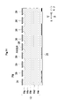
- FIG. 4 is a cross-sectional view of the antenna element 10a.
- the antenna element 10a differs from the antenna element 10 in the following three points.
- a low dielectric constant material 30 having a dielectric constant lower than that of the insulating base material 12 is provided in the plurality of first insulating base non-forming regions A1.
- a low dielectric constant material 32 having a dielectric constant lower than that of the insulating base material 12 is provided in the plurality of second insulating base non-formation regions A2.
- a low dielectric constant material 34 having a lower dielectric constant than the dielectric constant of the insulating base material 12 is provided in the insulating base non-formation region A0.
- the low dielectric constant materials 30, 32, 34 are, for example, materials in which low dielectric ceramic powder is mixed with resin.
- the rest of the structure of the antenna element 10a is the same as that of the antenna element 10, so the description is omitted.
- the antenna element 10a as described above has the same effects as the antenna element 10 does.
- the method for manufacturing the antenna element 10a further includes steps S6 and S7 in FIG. More specifically, each of the low dielectric constant materials 30 and 34 having a dielectric constant lower than that of the insulating base material 12 is filled into the plurality of first holes Sp1 and Sp0 (step S6, first filling step ). Furthermore, the low dielectric constant material 32 having a dielectric constant lower than that of the insulating base material 12 is filled into the plurality of second holes Sp2 (step S7, second filling step). In the first filling step and the second filling step, for example, each of the pastes of the low dielectric constant materials 30, 32, and 34 is squeegeeed into the plurality of first holes Sp1, the plurality of second holes Sp2, and the holes Sp0.
- FIG. 5 is a top view of the insulator layer 16a of the antenna element 10b.
- the antenna element 10b differs from the antenna element 10 in the structure of the antenna conductor layer 20, the number and shape of the first openings Op1, and the number and shape of the first insulating base non-formation regions A1. More specifically, the antenna conductor layer 20 and the reference conductor layer 24 are integrated. Thereby, the ground potential is connected to the antenna conductor layer 20 .
- the antenna element 10b has one first aperture Op1.
- the number of first insulating base non-formation regions A1 is one.
- the first opening Op1 has a belt shape extending in the front-rear direction when viewed in the vertical direction. The length of the first opening Op1 in the front-rear direction is approximately half the wavelength of the high-frequency signal transmitted and received by the antenna conductor layer 20 .
- the first insulating base non-formation region A1 has a strip shape extending in the front-rear direction when viewed in the vertical direction.
- the signal conductor layer 28 overlaps the first opening Op1 when viewed in the vertical direction.
- the signal conductor layer 28 is not connected to the antenna conductor layer 20 via an interlayer connection conductor.
- the antenna conductor layer 20 functions as a slot antenna.
- the rest of the structure of the antenna element 10b is the same as that of the antenna element 10, so the description is omitted. According to the antenna element 10b, the same effects as those of the antenna element 10 can be obtained.
- FIG. 6 is a top view of the insulator layer 16a of the antenna element 10c.
- FIG. 7 is a cross-sectional view of the antenna element 10c.
- the antenna element 10c differs from the antenna element 10 in that it includes a plurality of antenna conductor layers 20a to 20o.
- the antenna conductor layers 20a to 20o are provided on the upper main surface of the insulating base material 12. As shown in FIG. Accordingly, the antenna conductor layers 20a to 20o are provided on the upper main surface of the insulator layer 16a.
- the antenna conductor layers 20a to 20o are arranged in a matrix when viewed in the vertical direction. Although illustration is omitted, the antenna conductor layers 20a to 20o are electrically connected to signal conductor layers (not shown) via interlayer connection conductors v100. Since other structures of the antenna element 10c are the same as those of the antenna element 10, description thereof is omitted.
- the same effects as those of the antenna element 10 can be obtained. Further, by providing the first insulating base non-formation region A1 between the antenna conductor layers 20a to 20o, interference of high frequency signals between the antenna conductor layers 20a to 20o is suppressed. Furthermore, since the antenna conductor layers 20a to 20o can be brought closer, the size of the antenna element 10c can be reduced.
- FIG. 8 is a top view of the insulator layer 16a of the antenna element 10d.
- 9 and 10 are cross-sectional views of the antenna element 10d.
- the antenna element 10d differs from the antenna element 10 in that it includes antenna conductor layers 20a and 20b and reference conductor layers 22a and 22b.
- the antenna conductor layers 20a and 20b are provided on the upper main surface of the insulator layer 16a.
- the antenna conductor layers 20a and 20b are arranged in this order from left to right.
- the reference conductor layers 22a and 22b are provided on the lower main surface of the insulator layer 16e.
- the reference conductor layers 22a and 22b are provided in this order from left to right.
- the reference conductor layers 22a and 22b are electrically connected by conductor layers and interlayer connection conductors (not shown).
- This conductor layer is provided on the upper main surface of the insulator layer 16c.
- the reference conductor layers 22a, 22b, and 24 are electrically connected by conductor layers and interlayer connection conductors (not shown).
- the antenna element 10d has first sections A21, A23 and a second section A22.
- the first section A21, the second section A22 and the first section A23 are arranged in this order from left to right.
- the second section A22 is bent with respect to the first section A21 in the negative direction of the z-axis (vertical direction in the first section A21).
- the radius of curvature of the second section A22 is smaller than the radius of curvature of the first sections A21 and A23.
- the first sections A21 and A23 are not bent in the z-axis direction.
- the insulating base non-formed area A0 is located in the second section A22.
- the hole Sp0 is located in the second section A22.
- the insulating base non-formed region A0 and the holes Sp0 reach the signal conductor layer 28 .
- the insulating base material 12 is further provided with an insulating base material non-formation region A10 and holes Sp10.
- the insulating base non-formed region A10 and the holes Sp10 reach the signal conductor layer 28 .
- the vertical thickness of the antenna element 10d in the first sections A21 and A23 is greater than the vertical thickness of the antenna element 10d in the second section A22.
- the antenna element 10d can be easily bent in the z-axis direction in the second section A22.
- the rest of the structure of the antenna element 10d is the same as that of the antenna element 10, so description thereof will be omitted. According to the antenna element 10d, the same effect as the antenna element 10 can be obtained.
- FIG. 11 is a cross-sectional view of the antenna element 10e.
- the insulating base non-formed region A0 and the holes Sp0 do not reach the signal conductor layer 28, and the insulating base non-formed region A10 and the holes Sp10 reach the signal conductor layer 28. It differs from the antenna element 10d in that it does not.
- the rest of the structure of the antenna element 10e is the same as that of the antenna element 10d, so the description is omitted.
- the antenna element 10e can achieve the same effects as the antenna element 10d.
- FIG. 12 is a cross-sectional view of the antenna element 10f.
- the antenna element 10f differs from the antenna element 10e in that the insulating base non-formation region A10 and the air holes Sp10 are not provided. Since other structures of the antenna element 10f are the same as those of the antenna element 10e, description thereof is omitted.
- the antenna element 10f can provide the same effects as the antenna element 10e.
- FIG. 13 is a top view of the insulator layer 16a of the antenna element 10g.
- FIG. 14 is a cross-sectional view of the antenna element 10g.
- the antenna element 10 g differs from the antenna element 10 in the shape of the antenna conductor layer 20 and the shape of the reference conductor layer 24 . More specifically, the antenna conductor layer 20 has a meandering shape when viewed in the vertical direction. That is, the antenna conductor layer 20 meanders when viewed in the vertical direction. Further, the reference conductor layer 24 has an L shape when viewed in the vertical direction. Specifically, the reference conductor layer 24 extends in the front-rear direction on the left of the antenna conductor layer 20 and extends in the left-right direction behind the antenna conductor layer 20 . Since other structures of the antenna element 10g are the same as those of the antenna element 10, description thereof is omitted. According to the antenna element 10g, the same effects as those of the antenna element 10 can be obtained.
- the electrical length of the antenna conductor layer 20 is increased. Therefore, the frequency of the high-frequency signal that resonates in the antenna conductor layer 20 is lowered.
- FIG. 15 is a cross-sectional view of the antenna element 10h.
- the antenna element 10h differs from the antenna element 10 in that a protective layer 102 is further provided.
- the antenna conductor layer 20 is provided on the upper main surface of the insulating base material 12 .
- the protective layer 102 covers the antenna conductor layer 20 and is provided on the upper main surface of the insulating base material 12 .
- the material of the protective layer 102 is different from the material of the insulator layers 16a-16e. Accordingly, protective layer 102 is not part of insulating substrate 12 .
- the Young's modulus of the material of the protective layer 102 is, for example, greater than that of the material of the insulator layers 16a to 16e. Since other structures of the antenna element 10h are the same as those of the antenna element 10, description thereof is omitted. According to the antenna element 10h, the same effect as the antenna element 10 can be obtained.
- the antenna conductor layer 20 is protected and the structure of the holes Sp0 is protected. Further, when the dielectric constant of the protective layer 102 is higher than the dielectric constant of the insulator layers 16a to 16e, the frequency band of high-frequency signals that can be communicated by the antenna element 10h is widened. If the thickness of the protective layer 102 in the vertical direction is approximately the same as the wavelength of the high-frequency signal, the dielectric constant of the protective layer 102 may be lower than that of the insulating layers 16a to 16e.
- FIG. 16 is a cross-sectional view of the antenna element 10i.
- FIG. 17 is a top view of the antenna element 10i.
- FIG. 18 is a cross-sectional view of the antenna element 10i during manufacture.
- the antenna element 10i differs from the antenna element 10 in that it has a horn antenna structure.
- the antenna conductor layer 20 is provided on the upper main surface of the insulator layer 16b. However, as shown in FIG. 18, the upper surface of the insulator layer 16b is removed by etching before the insulator layers 16a-16e are crimped. At this time, the antenna conductor layer 20 is used as a mask. Therefore, under the antenna conductor layer 20 , the insulator layer 16 b remains in contact with the antenna conductor layer 20 . However, below the outer edge E1 of the antenna conductor layer 20 is located an insulating base non-formation area A0 in which the insulating layer 16b does not exist. That is, below the outer edge E1 of the antenna conductor layer 20, the holes Sp0 are located.
- the insulator layer 16a positioned around the antenna conductor layer 20 when viewed in the vertical direction is removed. Thereby, a through hole H100 is formed in the insulator layer 16a.
- the through-hole H100 has a shape in which the area of the through-hole H100 increases upward in a cross section perpendicular to the vertical direction.
- a plated layer 110 is provided to cover the inner peripheral surface of the through hole H100.
- the plated layer 110 is electrically connected to the reference conductor layer 24 .
- the rest of the structure of the antenna element 10i is the same as that of the antenna element 10, so the description is omitted. According to the antenna element 10i, the same effect as the antenna element 10 can be obtained.
- the antenna conductor layer 20 since the antenna conductor layer 20 is surrounded by air, the antenna conductor layer 20 has high radiation efficiency. Further, since the antenna element 10i has a horn antenna structure, the antenna element 10i has high directivity.
- FIG. 19 is a cross-sectional view of the antenna element 10j.
- FIG. 20 is a cross-sectional view of the antenna element 10j during manufacture.
- the antenna element 10j differs from the antenna element 10i in that reference conductor layers 25 and 27 are further provided.
- the reference conductor layers 25 and 27 are provided below the reference conductor layer 24 .
- the reference conductor layers 25 and 27 are exposed through the through hole H100.
- the plated layer 110 covers the inner peripheral surface of the through hole H100 and the reference conductor layers 25 and 27 exposed on the inner peripheral surface of the through hole H100.
- the through holes H100 are formed in the insulator layers 16a and 16b after the insulator layers 16a to 16f are stacked and pressure-bonded. Then, the plated layer 110 is formed on the inner peripheral surface of the through hole H100.
- Other structures of the antenna element 10j are the same as those of the antenna element 10i, so description thereof is omitted.
- the antenna element 10j can have the same effect as the antenna element 10i.
- FIG. 21 is a cross-sectional view of the antenna element 10k.
- the antenna element 10k differs from the antenna element 10 in that the second opening Op2 and the second insulating base non-formation area A2 do not exist.
- the rest of the structure of the antenna element 10k is the same as that of the antenna element 10, so the explanation is omitted.
- the antenna element 10k can have the same effect as the antenna element 10 does.
- FIG. 22 is a cross-sectional view of the antenna element 10l.
- the antenna element 10l differs from the antenna element 10a in that it further includes a first protective layer 70a and a second protective layer 70b.
- the first protective layer 70 a covers the upper main surface (first main surface) of the insulating base material 12 .
- the dielectric constant of the first protective layer 70 a is greater than that of the insulating base material 12 .
- the second protective layer 70 b covers the lower main surface (second main surface) of the insulating base material 12 .
- the dielectric constant of the second protective layer 70b is greater than that of the insulating base material 12 .
- Other structures of the antenna element 10d are the same as those of the antenna element 10a.
- the antenna element 10l can have the same effect as the antenna element 10a.
- the first protective layer 70 a covers the upper main surface (first main surface) of the insulating base material 12 . Therefore, the effect of shortening the wavelength of the high-frequency signal transmitted and received by the antenna conductor layer 20 is increased. Also, the antenna conductor layer 20 is protected by the first protective layer 70a. In addition, it is possible to simultaneously perform the filling of the material into the first insulating base non-formation region A1 and the second insulating base non-formation region A2 and the formation of the first protective layer 70a.
- FIG. 23 is a cross-sectional view of the antenna element 10m.
- the antenna element 10m is different from the antenna element 10l in that the first protective layer 70a is provided with a plurality of through holes h1 and the second protective layer 70b is provided with a plurality of through holes h2. differ from A through hole h1 is provided in a portion overlapping with one or more first openings Op1 and holes Sp0 in the first protective layer 70a when viewed in the vertical direction.
- the through hole h1 vertically penetrates the first protective layer 70a.
- the diameter of the through hole h1 is smaller than the diameter of the first opening Op1.
- Through holes h2 are provided in portions overlapping with the one or more second openings Op2 in the second protective layer 70b when viewed in the vertical direction.
- the diameter of the through hole h2 is smaller than the diameter of the second opening Op2.
- Other structures of the antenna element 10m are the same as those of the antenna element 10l.
- the antenna element 10m can have the same effect as the antenna element 10l.
- the through holes h1 are provided in the first protective layer 70a, the air in the first holes Sp1 can enter and exit. Therefore, even if the air inside the first holes Sp1 expands or contracts due to temperature changes such as reflow, the first protective layer 70 is less likely to peel off from the insulating base material 12 .
- FIG. 24 is a cross-sectional view of the antenna element 10n.
- the antenna element 10n differs from the antenna element 10k in that it further includes a first protective layer 70a.
- the first protective layer 70 a covers the upper main surface (first main surface) of the insulating base material 12 .
- the dielectric constant of the first protective layer 70 a is greater than that of the insulating base material 12 .
- the vertical thickness of the first protective layer 70a of the antenna element 10n is greater than the vertical thickness of the first protective layer 70a of the antenna element 10l.
- Other structures of antenna element 10n are the same as antenna element 10l.
- the antenna element 10n can have the same effect as the antenna element 10k.
- the first protective layer 70 a covers the upper main surface (first main surface) of the insulating base material 12 . Therefore, the effect of shortening the wavelength of the high-frequency signal transmitted and received by the antenna conductor layer 20 is increased. Also, the antenna conductor layer 20 is protected by the first protective layer 70a. In addition, it is possible to fill the insulating base non-formation region A0, the first insulating base non-formation region A1, and the second insulating base non-formation region A2 with the material and form the first protective layer 70a at the same time. .
- FIG. 25 is a cross-sectional view of the antenna element 10o.
- the antenna element 10o differs from the antenna element 10d in that the insulator layers 16a to 16e in the second section A22 are not removed.
- the rest of the structure of the antenna element 10o is the same as that of the antenna element 10d, so the description is omitted.
- the signal conductor layer 28 of the second section A22 is protected by the insulator layers 16a-16e.
- the resin etching of the second section A22 of the insulating base material 12 is not performed. The dry film is removed after resin etching.
- FIG. 26 is an exploded perspective view of the antenna element 10p.
- the antenna element 10p differs from the antenna element 10 in that the antenna conductor layers 20a and 20b are dipole antennas. Therefore, the antenna element 10h does not have the reference conductor layer 22.
- FIG. Each of the antenna conductor layers 20a and 20b is provided on the upper main surface of the insulator layer 16a.
- the antenna conductor layers 20a and 20b have a strip shape extending in the front-rear direction.
- a signal conductor layer 55a is connected to the antenna conductor layer 20a.
- a signal conductor layer 55b is connected to the antenna conductor layer 20b via an interlayer connection conductor v11.
- a plurality of first openings Op1 are provided in each of the antenna conductor layers 20a and 20b. Further, the insulator layer 16a is provided with a plurality of first insulating base non-formation regions A1. The rest of the structure of the antenna element 10p is the same as that of the antenna element 10, so the description is omitted. The antenna element 10p can have the same effect as the antenna element 10. FIG.
- circuit board 200 The circuit board 200 will be described below with reference to the drawings. 27 is a rear view of the circuit board 200. FIG.
- the circuit board 200 has a first section A111 and a second section A112.
- An antenna conductor layer 20 is provided in the first section A111. That is, the first section A111 has the same structure as the antenna elements 10, 10a-10h.
- the antenna conductor layer 20 is not provided in the second section A112. However, a signal conductor layer electrically connected to the antenna conductor layer 20 is provided.
- the first section A111 is not curved.
- the second section A112 is curved. However, the first section A111 may be curved. In this case, the radius of curvature of the first section A111 is greater than the radius of curvature of the second section A112.
- Holes Sp0a to Sp0f of antenna elements according to other modifications will be described below with reference to the drawings.
- 28 to 34 are cross-sectional views of holes Sp0a to Spg, respectively.
- the portion of the hole Sp0a having the maximum width in the direction perpendicular to the vertical direction may be located below the upper main surface of the insulator layer 16a.
- the air hole Sp0b may have a conical shape that is inverted upside down.
- the hole Sp0c may have a truncated cone shape that is inverted upside down.
- the holes Sp0d may be formed in a plurality of insulator layers 16a and 16b.
- the vacancies Sp0e may vertically penetrate between the upper main surface of the insulator layer 16a and the lower main surface of the insulator layer 16d.
- an insulator layer 116a may be provided between the insulator layers 16a and 16b.
- the material of the insulator layer 116a is, for example, fluororesin. Therefore, the insulator layer 116a is less likely to be removed by etching than the insulator layer 16a. Therefore, the vacancies Sp0f vertically penetrate only the insulator layer 16a.
- a through hole H120 may be formed in the insulator layer 116a. In this case, the vacancies Sp0g are formed in the insulator layers 16a and 16b.
- a conductor layer that is not etched may be provided instead of the insulator layer 116a in FIGS.
- the antenna elements according to the present invention are not limited to the antenna elements 10, 10a to 10p, and can be modified within the scope of the gist thereof.
- the configurations of the antenna elements 10, 10a to 10p may be combined arbitrarily.
- the holes Sp0, Sp0a to Sp0g may be formed by resin etching. In this case, processing of the insulator layers 16a and 16e is easy. Also, the holes Sp0, Sp0a to Sp0g may be formed by laser beam irradiation. In this case, the insulating layers 16a and 16e under the conductor layers can be scraped off by heat. Also, the holes Sp0, Sp0a to Sp0g may be formed by a combination of laser beam irradiation and resin etching. In this case, small diameter and deep holes can be formed.
- reference conductor layers 22, 24, and 26 are not essential components.
- the antenna conductor layer may be a dipole antenna or the like.
- the antenna conductor layer has a shape other than a rectangular shape, such as a linear shape.
- the antenna elements 10i to 10k may have a plurality of antenna conductor layers.
- At least a portion of the outer edge E1 of the antenna conductor should overlap the insulating base material non-formation area A0 when viewed in the vertical direction and should not be in contact with the insulating base material 12 .
- at least a portion of the inner edge E2 of the reference conductor layer 24 should overlap the insulating base non-formation region A0 when viewed in the vertical direction and should not be in contact with the insulating base 12 .
- An insulator layer may be further provided on the antenna conductor layer 20 .
- the material of this insulator layer may be the same material as the insulator layers 16a-16e. However, this insulator layer is not part of the insulating substrate 12 .
- the insulating base material 12 does not have to be flexible.
- the material of the insulating base material 12 may be a material other than a thermoplastic resin.
- the insulator layers 16a to 16f may be joined by an adhesive layer made of a material different from the material of the insulator layers 16a to 16f.
- a layer of the same material as the insulator layers 16a to 16d may be laminated on the upper main surface of the insulating base material 12. In this case, this layer is not part of the insulating substrate 12 . That is, the layers laminated above the upper main surface of the insulating base 12 on which the antenna conductor layer 20 is provided are not part of the insulating base 12 .
- the material filled in the first insulating base non-formation region A1 and the second insulating base non-formation region A2 is different from the material of the first protective layer 70a and the material of the second protective layer 70b. may be
Abstract
The present invention provides an antenna element. An insulating base material has a first main surface and a second main surface, aligned in the vertical direction. One or more antenna conductor layers are provided on the first main surface of the insulating base material. An area in which the insulating base material is not formed is positioned between the insulating base material and the antenna conductor layer in the vertical direction. An insulator layer is not present in the area in which the insulating base material is not formed. If viewed in the vertical direction, at least a portion of an outer edge of one or more antenna conductors overlap the area in which the insulating base material is not formed and does not contact the insulating base material. One or more areas in which the insulating base material is not formed is a vacancy.
Description
本発明は、アンテナ導体層を備えるアンテナ素子に関する。
The present invention relates to an antenna element provided with an antenna conductor layer.
従来のアンテナ素子に関する発明としては、例えば、特許文献1に記載のマイクロストリップアンテナが知られている。このマイクロストリップアンテナは、誘電体基板、方形状導体及び接地導体を備えている。誘電体基板は、上主面及び下主面を有している。方形状導体は、誘電体基板の上主面に設けられている。接地導体は、誘電体基板の下主面に設けられている。方形状導体は、上下方向に見て、接地導体と重なっている。このようなマイクロストリップアンテナでは、方形状導体がアンテナとして機能する。
As an invention related to conventional antenna elements, for example, the microstrip antenna described in Patent Document 1 is known. This microstrip antenna comprises a dielectric substrate, a rectangular conductor and a ground conductor. The dielectric substrate has an upper major surface and a lower major surface. A rectangular conductor is provided on the upper main surface of the dielectric substrate. A ground conductor is provided on the lower main surface of the dielectric substrate. The rectangular conductor overlaps the ground conductor when viewed in the vertical direction. In such a microstrip antenna, a rectangular conductor functions as an antenna.
ところで、特許文献1に記載のマイクロストリップアンテナにおいて、上下方向に見て方形状導体の外縁に電界集中が発生する場合がある。このような電界集中が発生すると、例えば、方形状導体の周囲に存在する導体と方形状導体とが電界結合しやすくなる。この場合、方形状導体から方形状導体の周囲に存在する導体に向かって電磁波が放射されやすくなる。その結果、マイクロストリップアンテナの放射効率が低下する。
By the way, in the microstrip antenna described in Patent Document 1, electric field concentration may occur at the outer edge of the rectangular conductor when viewed in the vertical direction. When such electric field concentration occurs, for example, electric field coupling between the conductors existing around the rectangular conductor and the rectangular conductor is likely to occur. In this case, electromagnetic waves are likely to be radiated from the rectangular conductor toward conductors present around the rectangular conductor. As a result, the radiation efficiency of the microstrip antenna is reduced.
そこで、本発明の目的は、アンテナ素子の放射効率の低下を抑制できるアンテナ素子及び電子機器を提供することである。
Accordingly, an object of the present invention is to provide an antenna element and an electronic device capable of suppressing a decrease in the radiation efficiency of the antenna element.
本発明の一形態に係るアンテナ素子は、
アンテナ素子であって、
上下方向に並んでいる第1主面及び第2主面を有している絶縁基材と、
前記絶縁基材の第1主面に設けられている1以上のアンテナ導体層と、
を備えており、
絶縁基材非形成領域が、上下方向において前記絶縁基材と前記アンテナ導体層との間に位置しており、
前記絶縁基材非形成領域には、前記絶縁基材が存在せず、
前記1以上のアンテナ導体の外縁の少なくとも一部分は、上下方向に見て前記絶縁基材非形成領域と重なり、前記絶縁基材と接触しておらず、
前記アンテナ素子は、(A)又は(B)の構造を有しており、(A)前記1以上の絶縁基材非形成領域は、空孔である、(B)前記1以上の絶縁基材非形成領域には、前記絶縁基材の誘電率より低い誘電率を有する低誘電率材料が設けられている。 An antenna element according to one aspect of the present invention includes:
An antenna element,
an insulating base material having a first principal surface and a second principal surface aligned in the vertical direction;
one or more antenna conductor layers provided on the first main surface of the insulating base;
and
an insulating base non-formed region is positioned between the insulating base and the antenna conductor layer in the vertical direction;
The insulating base does not exist in the insulating base non-formation region,
at least a portion of the outer edge of the one or more antenna conductors overlaps the insulating base non-formed region when viewed in the vertical direction and is not in contact with the insulating base;
The antenna element has the structure (A) or (B), and (A) the one or more insulating base non-forming regions are voids, and (B) the one or more insulating bases. A low dielectric constant material having a dielectric constant lower than that of the insulating substrate is provided in the non-forming region.
本発明に係るアンテナ素子及び電子機器によれば、アンテナ素子の放射効率の低下を抑制できる。
According to the antenna element and the electronic device according to the present invention, it is possible to suppress the deterioration of the radiation efficiency of the antenna element.
(実施形態)[アンテナ素子の構造]
以下に、本発明の実施形態に係るアンテナ素子10の構造について図面を参照しながら説明する。図1は、アンテナ素子10の分解斜視図である。なお、図1では、複数の層間接続導体v1、複数の第1開口Op1、複数の第2開口Op2、複数の第1絶縁基材非形成領域A1、複数の第2絶縁基材非形成領域A2、複数の第1空孔Sp1及び複数の第2空孔Sp2の内の代表的な層間接続導体v1、第1開口Op1、第2開口Op2、第1絶縁基材非形成領域A1、第2絶縁基材非形成領域A2、第1空孔Sp1及び第2空孔Sp2にのみ参照符号を付した。図2は、アンテナ素子10を備える電子機器1の断面図である。図2は、図1のA-Aにおける断面図である。ただし、図2には、図1に示されていない筐体100を示した。 (Embodiment) [Structure of Antenna Element]
The structure of theantenna element 10 according to the embodiment of the present invention will be described below with reference to the drawings. FIG. 1 is an exploded perspective view of the antenna element 10. FIG. In FIG. 1, a plurality of interlayer connection conductors v1, a plurality of first openings Op1, a plurality of second openings Op2, a plurality of first insulating base non-forming regions A1, and a plurality of second insulating base non-forming regions A2 , a representative interlayer connection conductor v1 among the plurality of first holes Sp1 and the plurality of second holes Sp2, the first opening Op1, the second opening Op2, the first insulating base non-formed area A1, the second insulating Reference numerals are attached only to the base material non-forming region A2, the first holes Sp1, and the second holes Sp2. FIG. 2 is a cross-sectional view of the electronic device 1 including the antenna element 10. As shown in FIG. FIG. 2 is a cross-sectional view along AA in FIG. However, FIG. 2 shows the housing 100 that is not shown in FIG.
以下に、本発明の実施形態に係るアンテナ素子10の構造について図面を参照しながら説明する。図1は、アンテナ素子10の分解斜視図である。なお、図1では、複数の層間接続導体v1、複数の第1開口Op1、複数の第2開口Op2、複数の第1絶縁基材非形成領域A1、複数の第2絶縁基材非形成領域A2、複数の第1空孔Sp1及び複数の第2空孔Sp2の内の代表的な層間接続導体v1、第1開口Op1、第2開口Op2、第1絶縁基材非形成領域A1、第2絶縁基材非形成領域A2、第1空孔Sp1及び第2空孔Sp2にのみ参照符号を付した。図2は、アンテナ素子10を備える電子機器1の断面図である。図2は、図1のA-Aにおける断面図である。ただし、図2には、図1に示されていない筐体100を示した。 (Embodiment) [Structure of Antenna Element]
The structure of the
本明細書において、方向を以下のように定義する。アンテナ素子10の絶縁基材12の上主面及び下主面の法線が延びている方向を上下方向と定義する。上下方向は、絶縁基材12の積層方向と一致する。また、アンテナ素子10のアンテナ導体層20の長辺が延びる方向を左右方向と定義する。アンテナ素子10のアンテナ導体層20の短辺が延びる方向を前後方向と定義する。上下方向は、前後方向に直交する。左右方向は、上下方向及び前後方向に直交する。
In this specification, directions are defined as follows. The vertical direction is defined as the direction in which the normal lines of the upper and lower main surfaces of the insulating base material 12 of the antenna element 10 extend. The vertical direction coincides with the stacking direction of the insulating base material 12 . Further, the direction in which the long side of the antenna conductor layer 20 of the antenna element 10 extends is defined as the horizontal direction. The direction in which the short side of the antenna conductor layer 20 of the antenna element 10 extends is defined as the front-rear direction. The up-down direction is perpendicular to the front-rear direction. The left-right direction is orthogonal to the up-down direction and the front-rear direction.
以下では、Xは、アンテナ素子10の部品又は部材である。本明細書において、特に断りのない場合には、Xの各部について以下のように定義する。Xの前部とは、Xの前半分を意味する。Xの後部とは、Xの後半分を意味する。Xの左部とは、Xの左半分を意味する。Xの右部とは、Xの右半分を意味する。Xの上部とは、Xの上半分を意味する。Xの下部とは、Xの下半分を意味する。Xの前端とは、Xの前方向の端を意味する。Xの後端とは、Xの後方向の端を意味する。Xの左端とは、Xの左方向の端を意味する。Xの右端とは、Xの右方向の端を意味する。Xの上端とは、Xの上方向の端を意味する。Xの下端とは、Xの下方向の端を意味する。Xの前端部とは、Xの前端及びその近傍を意味する。Xの後端部とは、Xの後端及びその近傍を意味する。Xの左端部とは、Xの左端及びその近傍を意味する。Xの右端部とは、Xの右端及びその近傍を意味する。Xの上端部とは、Xの上端及びその近傍を意味する。Xの下端部とは、Xの下端及びその近傍を意味する。
In the following, X is a part or member of the antenna element 10. In this specification, unless otherwise specified, each part of X is defined as follows. By front of X is meant the front half of X. Back of X means the back half of X. The left part of X means the left half of X. The right part of X means the right half of X. Top of X means the top half of X. The lower part of X means the lower half of X. The leading edge of X means the leading edge of X. The trailing end of X means the trailing end of X. The left end of X means the end of X in the left direction. The right end of X means the end of X in the right direction. The upper end of X means the end of X in the upward direction. The lower end of X means the lower end of X. The front end of X means the front end of X and its vicinity. The rear end of X means the rear end of X and its vicinity. The left end of X means the left end of X and its vicinity. The right end of X means the right end of X and its vicinity. The upper end of X means the upper end of X and its vicinity. The lower end of X means the lower end of X and its vicinity.
まず、図1を参照しながら、アンテナ素子10の構造について説明する。アンテナ素子10は、図1に示すように、絶縁基材12、アンテナ導体層20、リファレンス導体層22,24,26、信号導体層28、複数の層間接続導体v1及び層間接続導体v2を備えている。
First, the structure of the antenna element 10 will be described with reference to FIG. As shown in FIG. 1, the antenna element 10 includes an insulating base material 12, an antenna conductor layer 20, reference conductor layers 22, 24 and 26, a signal conductor layer 28, a plurality of interlayer connection conductors v1 and interlayer connection conductors v2. there is
絶縁基材12は、板形状を有している。従って、絶縁基材12は、上下方向に並んでいる上主面(第1主面)及び下主面(第2主面)を有している。絶縁基材12の上主面及び下主面は、左右方向に延びる長辺を有する長方形状を有している。従って、絶縁基材12の左右方向における長さは、絶縁基材12の前後方向における長さより長い。
The insulating base material 12 has a plate shape. Therefore, the insulating base material 12 has an upper principal surface (first principal surface) and a lower principal surface (second principal surface) which are aligned in the vertical direction. The upper main surface and the lower main surface of the insulating base material 12 have a rectangular shape with long sides extending in the left-right direction. Therefore, the length of the insulating base material 12 in the left-right direction is longer than the length of the insulating base material 12 in the front-rear direction.
絶縁基材12は、図1に示すように、絶縁体層16a~16eを含んでいる。絶縁基材12は、絶縁体層16a~16eが上下方向に積層された構造を有している。絶縁体層16a~16eは、上から下へとこの順に並んでいる。絶縁体層16a~16eは、上下方向に見て、絶縁基材12と同じ長方形状を有している。絶縁体層16a~16eは、可撓性を有する誘電体シートである。絶縁基材12の材料は、例えば、熱可塑性樹脂である。熱可塑性樹脂は、例えば、液晶ポリマー、PTFE(ポリテトラフロオロエチレン)等の熱可塑性樹脂である。絶縁基材12の材料は、ポリイミドであってもよい。絶縁基材12は可撓性を有する。そのため、アンテナ素子10は、折り曲げられて用いられてもよい。「アンテナ素子10が折り曲げられる」とは、アンテナ素子10に外力が加えられることによりアンテナ素子10が変形して曲がっていることを意味する。変形は、弾性変形でもよいし、塑性変形でもよいし、弾性変形及び塑性変形でもよい。
The insulating base material 12 includes insulator layers 16a to 16e, as shown in FIG. The insulating base material 12 has a structure in which insulating layers 16a to 16e are stacked vertically. The insulator layers 16a-16e are arranged in this order from top to bottom. The insulator layers 16a to 16e have the same rectangular shape as the insulating base material 12 when viewed in the vertical direction. The insulator layers 16a-16e are flexible dielectric sheets. The material of the insulating base material 12 is, for example, a thermoplastic resin. Thermoplastic resins are, for example, thermoplastic resins such as liquid crystal polymer and PTFE (polytetrafluoroethylene). The material of the insulating base material 12 may be polyimide. The insulating base material 12 has flexibility. Therefore, the antenna element 10 may be used while being bent. “The antenna element 10 is bent” means that the antenna element 10 is deformed and bent by applying an external force to the antenna element 10 . The deformation may be elastic deformation, plastic deformation, or both elastic deformation and plastic deformation.
アンテナ導体層20は、絶縁基材12の上主面又は下主面に設けられている。本実施形態では、アンテナ導体層20は、絶縁基材12の上主面に設けられている。アンテナ導体層20は、絶縁体層16a(第1絶縁体層)の上主面に設けられている。アンテナ導体層20は、上下方向に見て、左右方向に延びる長辺を有する長方形状を有している。アンテナ導体層20は、前後方向に延びる短辺及び左右方向に延びる長辺の両方で共振する。そこで、アンテナ導体層20の前後方向に延びる短辺及び左右方向に延びる長辺は、アンテナ導体層20が送受信する高周波信号の波長の約半分の長さである。アンテナ導体層20が送受信する高周波信号の波長の長さは、絶縁基材12の誘電率による波長短縮効果を考慮した波長である。アンテナ導体層20は、高周波信号を電磁波として放射する。また、アンテナ導体層20は、電磁波の高周波信号を受信する。
The antenna conductor layer 20 is provided on the upper main surface or the lower main surface of the insulating base material 12 . In this embodiment, the antenna conductor layer 20 is provided on the upper main surface of the insulating base material 12 . The antenna conductor layer 20 is provided on the upper main surface of the insulator layer 16a (first insulator layer). The antenna conductor layer 20 has a rectangular shape with long sides extending in the horizontal direction when viewed in the vertical direction. The antenna conductor layer 20 resonates on both the short side extending in the front-rear direction and the long side extending in the left-right direction. Therefore, the short side extending in the front-rear direction and the long side extending in the left-right direction of the antenna conductor layer 20 are about half the wavelength of the high-frequency signal transmitted and received by the antenna conductor layer 20 . The length of the wavelength of the high-frequency signal transmitted and received by the antenna conductor layer 20 is the wavelength in consideration of the wavelength shortening effect due to the dielectric constant of the insulating base material 12 . The antenna conductor layer 20 radiates high frequency signals as electromagnetic waves. Further, the antenna conductor layer 20 receives high-frequency signals of electromagnetic waves.
信号導体層28は、絶縁基材12に設けられている。本実施形態では、信号導体層28は、絶縁体層16cの上主面に設けられている。信号導体層28は、左右方向に延びている線形状を有している。信号導体層28の右端部は、上下方向に見て、アンテナ導体層20と重なっている。信号導体層28は、高周波信号を伝送する。
The signal conductor layer 28 is provided on the insulating base material 12 . In this embodiment, the signal conductor layer 28 is provided on the upper main surface of the insulator layer 16c. The signal conductor layer 28 has a linear shape extending in the left-right direction. The right end portion of the signal conductor layer 28 overlaps the antenna conductor layer 20 when viewed in the vertical direction. The signal conductor layer 28 transmits high frequency signals.
層間接続導体v2は、アンテナ導体層20と信号導体層28とを電気的に接続している。より詳細には、層間接続導体v2は、絶縁体層16a,16bを上下方向に貫通している。層間接続導体v2の上端は、アンテナ導体層20に接続されている。アンテナ導体層20において層間接続導体v2が接続されている位置は、高周波信号の給電点である。層間接続導体v2の下端は、信号導体層28の右端部に接続されている。
The interlayer connection conductor v2 electrically connects the antenna conductor layer 20 and the signal conductor layer . More specifically, the interlayer connection conductor v2 penetrates the insulator layers 16a and 16b in the vertical direction. An upper end of the interlayer connection conductor v2 is connected to the antenna conductor layer 20 . The position where the interlayer connection conductor v2 is connected in the antenna conductor layer 20 is a feeding point for high frequency signals. The lower end of the interlayer connection conductor v2 is connected to the right end of the signal conductor layer 28 .
リファレンス導体層22は、絶縁基材12に設けられ、かつ、アンテナ導体層20の下に設けられている。本実施形態では、リファレンス導体層22は、絶縁体層16eの下主面に設けられている。リファレンス導体層22は、上下方向に見て、アンテナ導体層20と重なっている。リファレンス導体層22は、上下方向に見て、左右方向に延びる長辺を有する長方形状を有している。リファレンス導体層22は、上下方向に見て、アンテナ導体層20の前後方向及び左右方向にはみ出している。すなわち、リファレンス導体層22の外縁は、上下方向に見て、アンテナ導体層20の外縁を包含している。
The reference conductor layer 22 is provided on the insulating base material 12 and below the antenna conductor layer 20 . In this embodiment, the reference conductor layer 22 is provided on the lower main surface of the insulator layer 16e. The reference conductor layer 22 overlaps the antenna conductor layer 20 when viewed in the vertical direction. The reference conductor layer 22 has a rectangular shape with long sides extending in the horizontal direction when viewed in the vertical direction. The reference conductor layer 22 protrudes from the antenna conductor layer 20 in the front-rear direction and the left-right direction when viewed in the vertical direction. That is, the outer edge of the reference conductor layer 22 includes the outer edge of the antenna conductor layer 20 when viewed in the vertical direction.
リファレンス導体層24は、絶縁基材12に設けられている。リファレンス導体層24は、アンテナ導体層20が絶縁基材12の上主面に設けられている場合には、絶縁基材12の上主面に設けられ、アンテナ導体層20が絶縁基材12の下主面に設けられている場合には、絶縁基材12の下主面に設けられている。本実施形態では、リファレンス導体層24は、絶縁基材12の上主面に設けられている。そして、リファレンス導体層24は、アンテナ導体層20が設けられている絶縁体層16aの上主面に設けられている。リファレンス導体層24は、上下方向に見て、長方形状の枠形状を有している。これにより、リファレンス導体層24は、上下方向に見て、アンテナ導体層20の周囲を囲んでいる。ただし、アンテナ導体層20とリファレンス導体層24とが短絡しないように、アンテナ導体層20とリファレンス導体層24とは離れている。
The reference conductor layer 24 is provided on the insulating base material 12 . The reference conductor layer 24 is provided on the upper main surface of the insulating base 12 when the antenna conductor layer 20 is provided on the upper main surface of the insulating base 12 . When provided on the lower main surface, it is provided on the lower main surface of the insulating base material 12 . In this embodiment, the reference conductor layer 24 is provided on the upper main surface of the insulating base material 12 . The reference conductor layer 24 is provided on the upper main surface of the insulator layer 16a on which the antenna conductor layer 20 is provided. The reference conductor layer 24 has a rectangular frame shape when viewed in the vertical direction. Thus, the reference conductor layer 24 surrounds the antenna conductor layer 20 when viewed in the vertical direction. However, the antenna conductor layer 20 and the reference conductor layer 24 are separated from each other so that the antenna conductor layer 20 and the reference conductor layer 24 are not short-circuited.
リファレンス導体層26は、絶縁基材12に設けられている。本実施形態では、リファレンス導体層26は、絶縁体層16cの上主面に設けられている。ただし、リファレンス導体層26の形状は、リファレンス導体層24と実質的に同じである。ただし、リファレンス導体層26と信号導体層28とが短絡しないように、リファレンス導体層26は、信号導体層28に接していない。
The reference conductor layer 26 is provided on the insulating base material 12 . In this embodiment, the reference conductor layer 26 is provided on the upper main surface of the insulator layer 16c. However, the shape of the reference conductor layer 26 is substantially the same as that of the reference conductor layer 24 . However, the reference conductor layer 26 is not in contact with the signal conductor layer 28 so that the reference conductor layer 26 and the signal conductor layer 28 are not short-circuited.
複数の層間接続導体v1は、リファレンス導体層22とリファレンス導体層24とリファレンス導体層26とを電気的に接続している。より詳細には、複数の層間接続導体v1は、絶縁体層16a~16eを上下方向に貫通している。複数の層間接続導体v1の上端は、リファレンス導体層24に接続されている。複数の層間接続導体v1の中間部は、リファレンス導体層26に接続されている。複数の層間接続導体v1の下端は、リファレンス導体層22に接続されている。複数の層間接続導体v1は、上下方向に見て、リファレンス導体層24に沿って並んでいる。すなわち、複数の層間接続導体v1は、上下方向に見て、アンテナ導体層20を囲むように並んでいる。
A plurality of interlayer connection conductors v1 electrically connect the reference conductor layer 22, the reference conductor layer 24, and the reference conductor layer . More specifically, the plurality of interlayer connection conductors v1 vertically penetrate through the insulator layers 16a to 16e. Upper ends of the plurality of interlayer connection conductors v1 are connected to the reference conductor layer 24 . Middle portions of the plurality of interlayer connection conductors v1 are connected to the reference conductor layer 26 . Lower ends of the plurality of interlayer connection conductors v1 are connected to the reference conductor layer 22 . The plurality of interlayer connection conductors v1 are arranged along the reference conductor layer 24 when viewed in the vertical direction. That is, the plurality of interlayer connection conductors v1 are arranged so as to surround the antenna conductor layer 20 when viewed in the vertical direction.
以上のようなアンテナ導体層20、リファレンス導体層22,24,26及び信号導体層28は、例えば、絶縁体層16a~16eの上主面又は下主面に設けられた金属箔にエッチングが施されることにより形成されている。金属箔は、例えば、銅箔である。また、層間接続導体v1,v2は、例えば、ビアホール導体である。ビアホール導体は、絶縁体層16a~16eに貫通孔を形成し、貫通孔に導電性ペーストを充填し、導電性ペーストを加熱により固化させることにより作製される。層間接続導体v1,v2は、例えば、スルーホール導体であってもよい。スルーホール導体は、絶縁体層16a~16eの一部又は全部を貫通する貫通孔を形成し、貫通孔にメッキを施すことにより作製される。
The antenna conductor layer 20, the reference conductor layers 22, 24, 26, and the signal conductor layer 28 as described above are formed by, for example, etching a metal foil provided on the upper or lower main surface of the insulator layers 16a to 16e. It is formed by being The metal foil is, for example, copper foil. Also, the interlayer connection conductors v1 and v2 are, for example, via-hole conductors. The via-hole conductors are produced by forming through-holes in the insulating layers 16a to 16e, filling the through-holes with a conductive paste, and solidifying the conductive paste by heating. The interlayer connection conductors v1 and v2 may be, for example, through-hole conductors. Through-hole conductors are produced by forming through-holes penetrating all or part of the insulator layers 16a to 16e and plating the through-holes.
次に、絶縁基材非形成領域A0及び空孔Sp0について説明する。絶縁基材非形成領域A0は、図2に示すように、絶縁基材12の上主面の一部が下方向に窪むことにより形成されている。絶縁基材非形成領域A0は、上下方向において絶縁基材12とアンテナ導体層20との間に位置している。すなわち、複数の絶縁基材非形成領域A0は、上下方向において絶縁体層16aとアンテナ導体層20との間に設けられている。これにより、絶縁基材非形成領域A0は、アンテナ導体層20及びリファレンス導体層24より下に位置している。絶縁基材非形成領域A0には、絶縁基材12が存在しない。本実施形態では、絶縁基材非形成領域A0は、空孔Sp0である。
Next, the insulating base material non-formation region A0 and the holes Sp0 will be described. As shown in FIG. 2, the insulating base material non-forming area A0 is formed by partially recessing the upper main surface of the insulating base material 12 downward. The insulating base non-formation region A0 is positioned between the insulating base 12 and the antenna conductor layer 20 in the vertical direction. That is, the plurality of insulating base non-formation regions A0 are provided between the insulator layer 16a and the antenna conductor layer 20 in the vertical direction. As a result, the insulating base non-formation region A0 is positioned below the antenna conductor layer 20 and the reference conductor layer 24. As shown in FIG. The insulating base material 12 does not exist in the insulating base material non-formation area A0. In this embodiment, the insulating base non-formation region A0 is the vacancy Sp0.
以下に、「外縁」及び「内縁」について説明する。本明細書において、例えば、アンテナ導体層20の外縁E1とは、上下方向に見て、アンテナ導体層20の外側に位置する縁を意味する。アンテナ導体層20の外縁E1より外側には、アンテナ導体層20が存在しない。本実施形態では、外縁E1は長方形状を有している。一方、本明細書において、例えば、リファレンス導体層24の内縁E2とは、上下方向に見て、リファレンス導体層24の内側に位置する縁を意味する。リファレンス導体層24の内縁E2は、リファレンス導体層24の外縁に囲まれた領域内に位置する。リファレンス導体層24の内縁E2より外側にはリファレンス導体層24が存在する。本実施形態では、内縁E2は長方形状を有している。内縁E2は、上下方向に見て、外縁E1を囲んでいる。また、内縁E2と外縁E1との距離は一定である。
The "outer edge" and "inner edge" will be explained below. In this specification, for example, the outer edge E1 of the antenna conductor layer 20 means an edge positioned outside the antenna conductor layer 20 when viewed in the vertical direction. The antenna conductor layer 20 does not exist outside the outer edge E1 of the antenna conductor layer 20 . In this embodiment, the outer edge E1 has a rectangular shape. On the other hand, in this specification, for example, the inner edge E2 of the reference conductor layer 24 means an edge located inside the reference conductor layer 24 when viewed in the vertical direction. The inner edge E2 of the reference conductor layer 24 is positioned within the area surrounded by the outer edge of the reference conductor layer 24 . The reference conductor layer 24 exists outside the inner edge E2 of the reference conductor layer 24 . In this embodiment, the inner edge E2 has a rectangular shape. The inner edge E2 surrounds the outer edge E1 when viewed in the vertical direction. Also, the distance between the inner edge E2 and the outer edge E1 is constant.
また、アンテナ導体層20の外縁E1とリファレンス導体層24の内縁E2との間には、導体非形成領域A11が形成されている。導体非形成領域A11は、導体が存在しない領域である。導体非形成領域A11は、上下方向に見て、長方形状の枠形状を有している。
In addition, a conductor non-formation area A11 is formed between the outer edge E1 of the antenna conductor layer 20 and the inner edge E2 of the reference conductor layer 24 . The conductor non-formation area A11 is an area in which no conductor exists. The conductor non-formation area A11 has a rectangular frame shape when viewed in the vertical direction.
絶縁基材非形成領域A0及び空孔Sp0は、上下方向に見て、アンテナ導体層20の外縁E1及びリファレンス導体層24の内縁E2に沿っている。すなわち、絶縁基材非形成領域A0及び空孔Sp0は、上下方向に見て、導体非形成領域A11と重なっている。従って、絶縁基材非形成領域A0及び空孔Sp0は、上下方向に見て、長方形状の枠形状を有している。これにより、絶縁基材非形成領域A0及び空孔Sp0は、上下方向に見て、アンテナ導体層20の周囲を囲んでいる。また、リファレンス導体層24は、上下方向に見て、絶縁基材非形成領域A0及び空孔Sp0の周囲を囲んでいる。
The insulating base non-formation region A0 and the holes Sp0 are along the outer edge E1 of the antenna conductor layer 20 and the inner edge E2 of the reference conductor layer 24 when viewed in the vertical direction. That is, the insulating base non-formation region A0 and the holes Sp0 overlap the conductor non-formation region A11 when viewed in the vertical direction. Therefore, the insulating base material non-formation region A0 and the holes Sp0 have a rectangular frame shape when viewed in the vertical direction. Thus, the insulating base non-formation region A0 and the holes Sp0 surround the antenna conductor layer 20 when viewed in the vertical direction. In addition, the reference conductor layer 24 surrounds the insulating base non-formed region A0 and the holes Sp0 when viewed in the vertical direction.
ただし、絶縁基材非形成領域A0及び空孔Sp0の内縁P1は、上下方向に見て、アンテナ導体層20と重なっている。これにより、アンテナ導体層20の外縁E1と絶縁基材12との間には空孔Sp0が存在している。その結果、アンテナ導体の外縁E1の全体は、上下方向に見て絶縁基材非形成領域A0と重なり、絶縁基材12と接触していない。
However, the insulating base non-formation region A0 and the inner edge P1 of the hole Sp0 overlap the antenna conductor layer 20 when viewed in the vertical direction. Thus, a hole Sp0 exists between the outer edge E1 of the antenna conductor layer 20 and the insulating base material 12. As shown in FIG. As a result, the entire outer edge E<b>1 of the antenna conductor overlaps the insulating base material non-formation region A<b>0 when viewed in the vertical direction and is not in contact with the insulating base material 12 .
また、絶縁基材非形成領域A0及び空孔Sp0の外縁P2は、上下方向に見て、リファレンス導体層24と重なっている。これにより、リファレンス導体層24の内縁E2と絶縁基材12との間には空孔Sp0が存在している。その結果、リファレンス導体層24の内縁E2の全体は、上下方向に見て絶縁基材非形成領域A0と重なり、絶縁基材12と接していない。
In addition, the outer edges P2 of the insulating base non-formation region A0 and the holes Sp0 overlap the reference conductor layer 24 when viewed in the vertical direction. Thus, a hole Sp0 exists between the inner edge E2 of the reference conductor layer 24 and the insulating base material 12. As shown in FIG. As a result, the entire inner edge E2 of the reference conductor layer 24 overlaps the insulating base non-formed region A0 when viewed in the vertical direction, and is not in contact with the insulating base 12 .
次に、複数の第1開口Op1、複数の第1絶縁基材非形成領域A1及び複数の第1空孔Sp1について説明する。複数の第1開口Op1は、アンテナ導体層20に設けられている。複数の第1開口Op1は、上下方向に見て、行列状に配置されている。複数の第1開口Op1は、上下方向に見て環状の外縁を有している。本実施形態では、複数の第1開口Op1は、上下方向に見て、円形状の外縁を有している。ただし、環状は、円環に限らず、長方形状や三角形状も含む。このように、環状の外縁は、端を有さない。従って、第1開口Op1は、切り欠きを含まない。切り欠きの外縁は、端を有している。切り欠きの外縁は、アンテナ導体層20の外縁の一部分が、アンテナ導体層20の中心に近づくように曲がっている部分である。従って、切り欠きの外縁は、アンテナ導体層20の一部である。第1開口Op1内には、アンテナ導体層20が存在しない。隣り合う複数の第1開口Op1の間隔は、例えば、アンテナ導体層20が送受信する高周波信号の波長の長さの1/4以下である。
Next, the plurality of first openings Op1, the plurality of first insulating base non-formation regions A1, and the plurality of first holes Sp1 will be described. A plurality of first openings Op1 are provided in the antenna conductor layer 20 . The plurality of first openings Op1 are arranged in a matrix when viewed in the vertical direction. The multiple first openings Op1 have annular outer edges when viewed in the vertical direction. In this embodiment, the plurality of first openings Op1 have circular outer edges when viewed in the vertical direction. However, an annular shape is not limited to a circular ring, and includes a rectangular shape and a triangular shape. Thus, the annular outer rim has no edges. Therefore, the first opening Op1 does not include a notch. The outer edge of the notch has edges. The outer edge of the notch is a part of the outer edge of the antenna conductor layer 20 that is bent toward the center of the antenna conductor layer 20 . Therefore, the outer edge of the notch is part of the antenna conductor layer 20 . The antenna conductor layer 20 does not exist within the first opening Op1. The interval between the plurality of adjacent first openings Op1 is, for example, 1/4 or less of the length of the wavelength of the high-frequency signal transmitted and received by the antenna conductor layer 20 .
複数の第1絶縁基材非形成領域A1は、絶縁基材12に設けられている。本実施形態では、複数の第1絶縁基材非形成領域A1は、絶縁体層16aに設けられている。これにより、複数の第1絶縁基材非形成領域A1は、アンテナ導体層20の下に位置している。複数の第1絶縁基材非形成領域A1には、絶縁基材12が存在しない。本実施形態では、複数の第1絶縁基材非形成領域A1は、第1空孔Sp1である。
A plurality of first insulating base non-formation regions A1 are provided on the insulating base 12 . In this embodiment, the plurality of first insulating base non-formation regions A1 are provided in the insulator layer 16a. As a result, the plurality of first insulating base non-formation regions A1 are positioned below the antenna conductor layer 20 . The insulating base material 12 does not exist in the plurality of first insulating base non-formed regions A1. In the present embodiment, the plurality of first insulating base non-formation regions A1 are the first holes Sp1.
複数の第1絶縁基材非形成領域A1は、複数の第1開口Op1に対応するように、上下方向に見て、行列状に配置されている。複数の第1絶縁基材非形成領域A1は、上下方向に見て環状の外縁を有している。本実施形態では、複数の第1絶縁基材非形成領域A1は、上下方向に見て、円形状の外縁を有している。ただし、複数の第1絶縁基材非形成領域A1のそれぞれは、上下方向に見て複数の第1開口Op1のそれぞれを包含している。すなわち、複数の第1開口Op1のそれぞれは、複数の第1絶縁基材非形成領域A1からはみ出していない。そのため、第1絶縁基材非形成領域A1の直径は、第1開口Op1の直径より大きい。また、第1絶縁基材非形成領域A1は、半球形状を有している。
The plurality of first insulating base non-formation regions A1 are arranged in a matrix when viewed in the vertical direction so as to correspond to the plurality of first openings Op1. The plurality of first insulating base non-formation regions A1 have annular outer edges when viewed in the vertical direction. In the present embodiment, the plurality of first insulating base non-formation regions A1 have circular outer edges when viewed in the vertical direction. However, each of the plurality of first insulating base non-formation regions A1 includes each of the plurality of first openings Op1 when viewed in the vertical direction. That is, each of the plurality of first openings Op1 does not protrude from the plurality of first insulating base non-formation regions A1. Therefore, the diameter of the first insulating base non-formation region A1 is larger than the diameter of the first opening Op1. In addition, the first insulating base non-formation region A1 has a hemispherical shape.
次に、複数の第2開口Op2、複数の第2絶縁基材非形成領域A2及び複数の第2空孔Sp2について説明する。複数の第2開口Op2、複数の第2絶縁基材非形成領域A2及び複数の第2空孔Sp2は、複数の第1開口Op1、複数の第1絶縁基材非形成領域A1及び複数の第1空孔Sp1と上下対称な構造を有している。そのため、複数の第2開口Op2、複数の第2絶縁基材非形成領域A2及び複数の第2空孔Sp2の説明を省略する。
Next, the plurality of second openings Op2, the plurality of second insulating base non-formation regions A2, and the plurality of second holes Sp2 will be described. The plurality of second openings Op2, the plurality of second insulating base non-forming regions A2, and the plurality of second holes Sp2 are formed by the plurality of first openings Op1, the plurality of first insulating base non-forming regions A1, and the plurality of second openings Op2. It has a vertically symmetrical structure with one vacancy Sp1. Therefore, description of the plurality of second openings Op2, the plurality of second insulating base non-formation regions A2, and the plurality of second holes Sp2 will be omitted.
電子機器1は、図2に示すように、アンテナ素子10及び筐体100を備えている。アンテナ素子10は、筐体100に収容される。電子機器1は、例えば、スマートフォン等の携帯型無線通信端末である。
The electronic device 1 includes an antenna element 10 and a housing 100, as shown in FIG. Antenna element 10 is housed in housing 100 . The electronic device 1 is, for example, a mobile wireless communication terminal such as a smart phone.
[アンテナ素子の製造方法]
以下に、アンテナ素子10の製造方法について図面を参照しながら説明する。図3は、アンテナ素子10の製造工程を示すフローチャートである。 [Manufacturing method of antenna element]
A method for manufacturing theantenna element 10 will be described below with reference to the drawings. FIG. 3 is a flow chart showing the manufacturing process of the antenna element 10. As shown in FIG.
以下に、アンテナ素子10の製造方法について図面を参照しながら説明する。図3は、アンテナ素子10の製造工程を示すフローチャートである。 [Manufacturing method of antenna element]
A method for manufacturing the
まず、上主面に金属箔が貼り付けられた絶縁体層16a~16cを準備する。同様に、下主面に金属箔が貼り付けられた絶縁体層16d,16eを準備する(ステップS1)。
First, insulator layers 16a to 16c with metal foil attached to the upper main surface are prepared. Similarly, insulator layers 16d and 16e having metal foil attached to their lower main surfaces are prepared (step S1).
次に、金属箔にマスクを形成し、エッチング処理を施すことにより、アンテナ導体層20、リファレンス導体層22,24,26及び信号導体層28を絶縁体層16a~16eに形成する(ステップS2)。
Next, a mask is formed on the metal foil and etching is performed to form the antenna conductor layer 20, the reference conductor layers 22, 24 and 26 and the signal conductor layer 28 on the insulator layers 16a to 16e (step S2). .
次に、絶縁体層16a~16eに複数の層間接続導体v1及び層間接続導体v2を形成する(ステップS3)。具体的には、絶縁体層16a~16eにレーザビームを照射して、複数の貫通孔を形成する。その後、複数の貫通孔に導電性ペーストを充填する。
Next, a plurality of interlayer connection conductors v1 and interlayer connection conductors v2 are formed on the insulator layers 16a to 16e (step S3). Specifically, the insulator layers 16a to 16e are irradiated with a laser beam to form a plurality of through holes. After that, the plurality of through holes are filled with a conductive paste.
次に、絶縁体層16a~16eを圧着することにより、絶縁基材12を形成する(ステップS4・圧着工程)。圧着工程では、絶縁体層16a~16eを上下方向に加圧しながら加熱する。これにより、絶縁体層16a~16eが軟化し、絶縁体層16a~16eが一体化される。また、導電性ペーストが加熱により固化し、複数の層間接続導体v1及び層間接続導体v2が形成される。
Next, the insulating base material 12 is formed by crimping the insulator layers 16a to 16e (step S4, crimping step). In the pressure bonding process, the insulator layers 16a to 16e are heated while being pressed vertically. As a result, the insulator layers 16a to 16e are softened, and the insulator layers 16a to 16e are integrated. Also, the conductive paste is solidified by heating to form a plurality of interlayer connection conductors v1 and interlayer connection conductors v2.
次に、空孔Sp0、複数の第1空孔Sp1及び複数の第2空孔Sp2のそれぞれを絶縁体層16a,16eに形成する(ステップS5)。具体的には、アンテナ導体層20をマスクとして絶縁体層16aにエッチングを施すことにより、空孔Sp0及び複数の第1空孔Sp1を形成する(第1空孔形成工程)。更に、リファレンス導体層22をマスクとして絶縁体層16eにエッチングを施すことにより、複数の第2空孔Sp2を形成する(第2空孔形成工程)。以上の工程を経て、アンテナ素子10が完成する。
Next, vacancies Sp0, a plurality of first vacancies Sp1, and a plurality of second vacancies Sp2 are formed in the insulator layers 16a and 16e (step S5). Specifically, by etching the insulator layer 16a using the antenna conductor layer 20 as a mask, the holes Sp0 and the plurality of first holes Sp1 are formed (first hole forming step). Furthermore, by etching the insulator layer 16e using the reference conductor layer 22 as a mask, a plurality of second holes Sp2 are formed (second hole forming step). Through the above steps, the antenna element 10 is completed.
[効果]
アンテナ素子10によれば、アンテナ素子10の放射効率の低下を抑制できる。アンテナ導体層20の外縁E1は、上下方向に見て絶縁基材非形成領域A0と重なり、絶縁基材12と接触していない。そして、絶縁基材非形成領域A0は、空孔Sp0である。これにより、アンテナ導体層20の外縁E1の周辺の誘電率が低くなる。そのため、アンテナ導体層20の外縁E1において電界集中が発生することが抑制される。その結果、アンテナ導体層20とリファレンス導体層24とが電界結合することが抑制される。以上より、アンテナ導体層20からリファレンス導体層24に向かって電磁波が放射されることが抑制され、マイクロストリップアンテナの放射効率の低下が抑制される。 [effect]
According to theantenna element 10, deterioration of the radiation efficiency of the antenna element 10 can be suppressed. The outer edge E<b>1 of the antenna conductor layer 20 overlaps the insulating base material non-formed area A<b>0 when viewed in the vertical direction and is not in contact with the insulating base material 12 . The insulating base non-formation region A0 is the hole Sp0. As a result, the dielectric constant around the outer edge E1 of the antenna conductor layer 20 is lowered. Therefore, the occurrence of electric field concentration at the outer edge E1 of the antenna conductor layer 20 is suppressed. As a result, electric field coupling between the antenna conductor layer 20 and the reference conductor layer 24 is suppressed. As described above, the radiation of electromagnetic waves from the antenna conductor layer 20 toward the reference conductor layer 24 is suppressed, and the deterioration of the radiation efficiency of the microstrip antenna is suppressed.
アンテナ素子10によれば、アンテナ素子10の放射効率の低下を抑制できる。アンテナ導体層20の外縁E1は、上下方向に見て絶縁基材非形成領域A0と重なり、絶縁基材12と接触していない。そして、絶縁基材非形成領域A0は、空孔Sp0である。これにより、アンテナ導体層20の外縁E1の周辺の誘電率が低くなる。そのため、アンテナ導体層20の外縁E1において電界集中が発生することが抑制される。その結果、アンテナ導体層20とリファレンス導体層24とが電界結合することが抑制される。以上より、アンテナ導体層20からリファレンス導体層24に向かって電磁波が放射されることが抑制され、マイクロストリップアンテナの放射効率の低下が抑制される。 [effect]
According to the
アンテナ素子10によれば、以下の理由によっても、アンテナ素子10の放射効率の低下を抑制できる。リファレンス導体層24の内縁E2は、上下方向に見て絶縁基材非形成領域A0と重なり、絶縁基材12と接触していない。そして、絶縁基材非形成領域A0は、空孔Sp0である。これにより、リファレンス導体層24の内縁E2の周辺の誘電率が低くなる。そのため、リファレンス導体層24の内縁E2において電界集中が発生することが抑制される。その結果、アンテナ導体層20とリファレンス導体層24とが電界結合することが抑制される。以上より、アンテナ導体層20からリファレンス導体層24に向かって電磁波が放射されることが抑制され、マイクロストリップアンテナの放射効率の低下が抑制される。
According to the antenna element 10, the deterioration of the radiation efficiency of the antenna element 10 can be suppressed also for the following reasons. The inner edge E2 of the reference conductor layer 24 overlaps the insulating base non-formed region A0 when viewed in the vertical direction, and is not in contact with the insulating base 12 . The insulating base non-formation region A0 is the hole Sp0. As a result, the dielectric constant around the inner edge E2 of the reference conductor layer 24 is lowered. Therefore, the occurrence of electric field concentration at the inner edge E2 of the reference conductor layer 24 is suppressed. As a result, electric field coupling between the antenna conductor layer 20 and the reference conductor layer 24 is suppressed. As described above, the radiation of electromagnetic waves from the antenna conductor layer 20 toward the reference conductor layer 24 is suppressed, and the deterioration of the radiation efficiency of the microstrip antenna is suppressed.
アンテナ素子10によれば、アンテナ素子10の薄型化を図ることができる。より詳細には、複数の第1絶縁基材非形成領域A1のそれぞれは、アンテナ導体層20の下に位置している。複数の第2絶縁基材非形成領域A2のそれぞれは、リファレンス導体層22の上に位置している。複数の第1絶縁基材非形成領域A1及び複数の第2絶縁基材非形成領域A2のそれぞれは、第1空孔Sp1及び第2空孔Sp2である。これにより、アンテナ導体層20とリファレンス導体層22との間の領域の誘電率が低下する。従って、設計値の容量をアンテナ導体層20とリファレンス導体層22との間に形成するために、アンテナ導体層20とリファレンス導体層22との距離を短くすることができる。これにより、アンテナ素子10の薄型化が図られる。
According to the antenna element 10, the thickness of the antenna element 10 can be reduced. More specifically, each of the plurality of first insulating base non-formation regions A1 is located below the antenna conductor layer 20 . Each of the plurality of second insulating base non-formation regions A2 is located on the reference conductor layer 22 . The plurality of first insulating base non-formation regions A1 and the plurality of second insulating base non-formation regions A2 are first holes Sp1 and second holes Sp2, respectively. This reduces the dielectric constant of the region between the antenna conductor layer 20 and the reference conductor layer 22 . Therefore, the distance between the antenna conductor layer 20 and the reference conductor layer 22 can be shortened in order to form the designed capacitance between the antenna conductor layer 20 and the reference conductor layer 22 . As a result, the thickness of the antenna element 10 can be reduced.
アンテナ素子10によれば、アンテナ素子10を容易に折り曲げることができる。より詳細には、アンテナ素子10では、複数の第1空孔Sp1、複数の第2空孔Sp2及び空孔Sp0が絶縁基材12に設けられている。これにより、アンテナ素子10が変形しやすくなる。また、前記の通りアンテナ素子10の薄型化が図られるので、アンテナ素子10が更に変形しやすくなる。その結果、アンテナ素子10によれば、アンテナ素子10を容易に折り曲げることができる。
According to the antenna element 10, the antenna element 10 can be easily bent. More specifically, in the antenna element 10, the insulating base 12 is provided with a plurality of first holes Sp1, a plurality of second holes Sp2, and a hole Sp0. This makes it easier for the antenna element 10 to deform. In addition, since the thickness of the antenna element 10 can be reduced as described above, the antenna element 10 can be more easily deformed. As a result, according to the antenna element 10, the antenna element 10 can be easily bent.
アンテナ素子10によれば、アンテナ素子10の放射効率を向上させることができる。より詳細には、前記の通り、アンテナ導体層20近傍の誘電率が小さくなるので、アンテナ導体層20を伝送される高周波信号の波長が長くなる。従って、アンテナ導体層20で高周波信号を共振させるために、アンテナ導体層20を大型化してもよい。アンテナ導体層20が大型化すると、アンテナ素子10の放射効率が向上する。
According to the antenna element 10, the radiation efficiency of the antenna element 10 can be improved. More specifically, as described above, since the dielectric constant near the antenna conductor layer 20 becomes smaller, the wavelength of the high-frequency signal transmitted through the antenna conductor layer 20 becomes longer. Therefore, the size of the antenna conductor layer 20 may be increased in order to resonate the high-frequency signal in the antenna conductor layer 20 . When the antenna conductor layer 20 is enlarged, the radiation efficiency of the antenna element 10 is improved.
アンテナ素子10の製造方法によれば、空孔Sp0を容易に形成できる。より詳細には、アンテナ導体層20及びリファレンス導体層24をマスクとして絶縁体層16aにエッチングを施すことにより、空孔Sp0を形成する。このように、アンテナ導体層20及びリファレンス導体層22をマスクとして利用することにより、空孔Sp0を形成するために、マスクを新たに形成する必要がない。その結果、アンテナ素子10の製造方法によれば、空孔Sp0を容易に形成できる。
According to the manufacturing method of the antenna element 10, the holes Sp0 can be easily formed. More specifically, the holes Sp0 are formed by etching the insulator layer 16a using the antenna conductor layer 20 and the reference conductor layer 24 as masks. By using the antenna conductor layer 20 and the reference conductor layer 22 as masks in this way, it is not necessary to form a new mask for forming the holes Sp0. As a result, according to the manufacturing method of the antenna element 10, the holes Sp0 can be easily formed.
絶縁基材12の材料が熱可塑性樹脂であるので、絶縁体層16a~16eの接合に熱可塑性樹脂とは異なる材料の接着剤層を用いる必要がない。これにより、熱圧着により絶縁基材12を容易に形成できる。また、絶縁基材12を容易に塑性変形させることができる。
Since the material of the insulating base material 12 is a thermoplastic resin, it is not necessary to use an adhesive layer made of a material different from the thermoplastic resin for joining the insulating layers 16a to 16e. Thereby, the insulating base material 12 can be easily formed by thermocompression bonding. Moreover, the insulating base material 12 can be easily plastically deformed.
(第1変形例)
以下に、第1変形例に係るアンテナ素子10aについて図面を参照しながら説明する。図4は、アンテナ素子10aの断面図である。 (First modification)
Anantenna element 10a according to a first modified example will be described below with reference to the drawings. FIG. 4 is a cross-sectional view of the antenna element 10a.
以下に、第1変形例に係るアンテナ素子10aについて図面を参照しながら説明する。図4は、アンテナ素子10aの断面図である。 (First modification)
An
アンテナ素子10aは、以下の3点においてアンテナ素子10と相違する。
The antenna element 10a differs from the antenna element 10 in the following three points.
・複数の第1絶縁基材非形成領域A1には、絶縁基材12の誘電率より低い誘電率を有する低誘電率材料30が設けられている。 ・複数の第2絶縁基材非形成領域A2には、絶縁基材12の誘電率より低い誘電率を有する低誘電率材料32が設けられている。 ・絶縁基材非形成領域A0には、絶縁基材12の誘電率より低い誘電率を有する低誘電率材料34が設けられている。
A low dielectric constant material 30 having a dielectric constant lower than that of the insulating base material 12 is provided in the plurality of first insulating base non-forming regions A1. · A low dielectric constant material 32 having a dielectric constant lower than that of the insulating base material 12 is provided in the plurality of second insulating base non-formation regions A2. · A low dielectric constant material 34 having a lower dielectric constant than the dielectric constant of the insulating base material 12 is provided in the insulating base non-formation region A0.
低誘電率材料30,32,34は、例えば、低誘電セラミックの粉末を樹脂に混合した材料である。アンテナ素子10aのその他の構造は、アンテナ素子10と同じであるので説明を省略する。以上のようなアンテナ素子10aは、アンテナ素子10と同じ作用効果を奏する。
The low dielectric constant materials 30, 32, 34 are, for example, materials in which low dielectric ceramic powder is mixed with resin. The rest of the structure of the antenna element 10a is the same as that of the antenna element 10, so the description is omitted. The antenna element 10a as described above has the same effects as the antenna element 10 does.
また、アンテナ素子10aの製造方法では、図3のステップS6及びステップS7を更に備えている。より詳細には、絶縁基材12の誘電率より低い誘電率を有する低誘電率材料30,34のそれぞれを複数の第1空孔Sp1及び空孔Sp0に充填する(ステップS6・第1充填工程)。更に、絶縁基材12の誘電率より低い誘電率を有する低誘電率材料32を複数の第2空孔Sp2に充填する(ステップS7・第2充填工程)。第1充填工程及び第2充填工程は、例えば、低誘電率材料30,32,34のペーストのそれぞれをスキージにより複数の第1空孔Sp1、複数の第2空孔Sp2及び空孔Sp0へと押し込むことにより実行される。このように、複数の第1空孔Sp1及び空孔Sp0に低誘電率材料30,34が充填されることにより、アンテナ導体層20の外縁E1及びリファレンス導体層24の内縁E2の変形が抑制される。
In addition, the method for manufacturing the antenna element 10a further includes steps S6 and S7 in FIG. More specifically, each of the low dielectric constant materials 30 and 34 having a dielectric constant lower than that of the insulating base material 12 is filled into the plurality of first holes Sp1 and Sp0 (step S6, first filling step ). Furthermore, the low dielectric constant material 32 having a dielectric constant lower than that of the insulating base material 12 is filled into the plurality of second holes Sp2 (step S7, second filling step). In the first filling step and the second filling step, for example, each of the pastes of the low dielectric constant materials 30, 32, and 34 is squeegeeed into the plurality of first holes Sp1, the plurality of second holes Sp2, and the holes Sp0. Executed by pushing. By filling the low dielectric constant materials 30 and 34 in the plurality of first holes Sp1 and Sp0 in this manner, deformation of the outer edge E1 of the antenna conductor layer 20 and the inner edge E2 of the reference conductor layer 24 is suppressed. be.
(第2変形例)
以下に、第2変形例に係るアンテナ素子10bについて図面を参照しながら説明する。図5は、アンテナ素子10bの絶縁体層16aの上面図である。 (Second modification)
Anantenna element 10b according to a second modified example will be described below with reference to the drawings. FIG. 5 is a top view of the insulator layer 16a of the antenna element 10b.
以下に、第2変形例に係るアンテナ素子10bについて図面を参照しながら説明する。図5は、アンテナ素子10bの絶縁体層16aの上面図である。 (Second modification)
An
アンテナ素子10bは、アンテナ導体層20の構造、第1開口Op1の数及び形状並びに第1絶縁基材非形成領域A1の数及び形状においてアンテナ素子10と相違する。より詳細には、アンテナ導体層20とリファレンス導体層24とが一体化されている。これにより、アンテナ導体層20には、グランド電位が接続されている。アンテナ素子10bでは、第1開口Op1の数は1個である。第1絶縁基材非形成領域A1の数は1個である。また、第1開口Op1は、上下方向に見て、前後方向に延びる帯形状を有している。第1開口Op1の前後方向の長さは、アンテナ導体層20が送受信する高周波信号の波長の約半分の長さである。第1絶縁基材非形成領域A1は、上下方向に見て、前後方向に延びる帯形状を有している。信号導体層28は、上下方向に見て、第1開口Op1と重なっている。ただし、信号導体層28は、アンテナ導体層20と層間接続導体を介して接続されていない。このようなアンテナ素子10bでは、アンテナ導体層20は、スロットアンテナとして機能する。アンテナ素子10bのその他の構造は、アンテナ素子10と同じであるので説明を省略する。アンテナ素子10bによれば、アンテナ素子10と同じ作用効果を奏することができる。
The antenna element 10b differs from the antenna element 10 in the structure of the antenna conductor layer 20, the number and shape of the first openings Op1, and the number and shape of the first insulating base non-formation regions A1. More specifically, the antenna conductor layer 20 and the reference conductor layer 24 are integrated. Thereby, the ground potential is connected to the antenna conductor layer 20 . The antenna element 10b has one first aperture Op1. The number of first insulating base non-formation regions A1 is one. In addition, the first opening Op1 has a belt shape extending in the front-rear direction when viewed in the vertical direction. The length of the first opening Op1 in the front-rear direction is approximately half the wavelength of the high-frequency signal transmitted and received by the antenna conductor layer 20 . The first insulating base non-formation region A1 has a strip shape extending in the front-rear direction when viewed in the vertical direction. The signal conductor layer 28 overlaps the first opening Op1 when viewed in the vertical direction. However, the signal conductor layer 28 is not connected to the antenna conductor layer 20 via an interlayer connection conductor. In such an antenna element 10b, the antenna conductor layer 20 functions as a slot antenna. The rest of the structure of the antenna element 10b is the same as that of the antenna element 10, so the description is omitted. According to the antenna element 10b, the same effects as those of the antenna element 10 can be obtained.
(第3変形例)
以下に、第3変形例に係るアンテナ素子10cについて図面を参照しながら説明する。図6は、アンテナ素子10cの絶縁体層16aの上面図である。図7は、アンテナ素子10cの断面図である。 (Third modification)
Anantenna element 10c according to a third modified example will be described below with reference to the drawings. FIG. 6 is a top view of the insulator layer 16a of the antenna element 10c. FIG. 7 is a cross-sectional view of the antenna element 10c.
以下に、第3変形例に係るアンテナ素子10cについて図面を参照しながら説明する。図6は、アンテナ素子10cの絶縁体層16aの上面図である。図7は、アンテナ素子10cの断面図である。 (Third modification)
An
アンテナ素子10cは、複数のアンテナ導体層20a~20oを備えている点においてアンテナ素子10と相違する。アンテナ導体層20a~20oは、絶縁基材12の上主面に設けられている。従って、アンテナ導体層20a~20oは、絶縁体層16aの上主面に設けられている。アンテナ導体層20a~20oは、上下方向に見て、行列状に配置されている。なお、図示を省略するが、アンテナ導体層20a~20oは、図示しない信号導体層に層間接続導体v100を介して電気的に接続されている。アンテナ素子10cのその他の構造は、アンテナ素子10と同じであるので説明を省略する。アンテナ素子10cによれば、アンテナ素子10と同じ作用効果を奏することができる。また、アンテナ導体層20a~20oの間に第1絶縁基材非形成領域A1が設けられることにより、アンテナ導体層20a~20o間の高周波信号の干渉が抑制される。更に、アンテナ導体層20a~20oを近づけることができるので、アンテナ素子10cの小型化が図られる。
The antenna element 10c differs from the antenna element 10 in that it includes a plurality of antenna conductor layers 20a to 20o. The antenna conductor layers 20a to 20o are provided on the upper main surface of the insulating base material 12. As shown in FIG. Accordingly, the antenna conductor layers 20a to 20o are provided on the upper main surface of the insulator layer 16a. The antenna conductor layers 20a to 20o are arranged in a matrix when viewed in the vertical direction. Although illustration is omitted, the antenna conductor layers 20a to 20o are electrically connected to signal conductor layers (not shown) via interlayer connection conductors v100. Since other structures of the antenna element 10c are the same as those of the antenna element 10, description thereof is omitted. According to the antenna element 10c, the same effects as those of the antenna element 10 can be obtained. Further, by providing the first insulating base non-formation region A1 between the antenna conductor layers 20a to 20o, interference of high frequency signals between the antenna conductor layers 20a to 20o is suppressed. Furthermore, since the antenna conductor layers 20a to 20o can be brought closer, the size of the antenna element 10c can be reduced.
(第4変形例)
以下に、第4変形例に係るアンテナ素子10dについて図面を参照しながら説明する。図8は、アンテナ素子10dの絶縁体層16aの上面図である。図9及び図10は、アンテナ素子10dの断面図である。 (Fourth modification)
Anantenna element 10d according to a fourth modification will be described below with reference to the drawings. FIG. 8 is a top view of the insulator layer 16a of the antenna element 10d. 9 and 10 are cross-sectional views of the antenna element 10d.
以下に、第4変形例に係るアンテナ素子10dについて図面を参照しながら説明する。図8は、アンテナ素子10dの絶縁体層16aの上面図である。図9及び図10は、アンテナ素子10dの断面図である。 (Fourth modification)
An
アンテナ素子10dは、アンテナ導体層20a,20b及びリファレンス導体層22a,22bを備えている点においてアンテナ素子10と相違する。アンテナ導体層20a,20bは、絶縁体層16aの上主面に設けられている。アンテナ導体層20a,20bは、左から右へとこの順に並んでいる。リファレンス導体層22a,22bは、絶縁体層16eの下主面に設けられている。リファレンス導体層22a,22bは、左から右へとこの順に設けられている。リファレンス導体層22a,22bは、図示しない導体層及び層間接続導体により電気的に接続されている。この導体層は、絶縁体層16cの上主面に設けられている。また、リファレンス導体層22a,22b,24は、図示しない導体層及び層間接続導体により電気的に接続されている。
The antenna element 10d differs from the antenna element 10 in that it includes antenna conductor layers 20a and 20b and reference conductor layers 22a and 22b. The antenna conductor layers 20a and 20b are provided on the upper main surface of the insulator layer 16a. The antenna conductor layers 20a and 20b are arranged in this order from left to right. The reference conductor layers 22a and 22b are provided on the lower main surface of the insulator layer 16e. The reference conductor layers 22a and 22b are provided in this order from left to right. The reference conductor layers 22a and 22b are electrically connected by conductor layers and interlayer connection conductors (not shown). This conductor layer is provided on the upper main surface of the insulator layer 16c. The reference conductor layers 22a, 22b, and 24 are electrically connected by conductor layers and interlayer connection conductors (not shown).
ここで、アンテナ素子10dは、第1区間A21,A23及び第2区間A22を有している。第1区間A21、第2区間A22及び第1区間A23は、左から右へとこの順に並んでいる。第2区間A22は、z軸の負方向(第1区間A21における上下方向)に第1区間A21に対して折れ曲がっている。第2区間A22の曲率半径は、第1区間A21,A23の曲率半径より小さい。本実施形態では、第1区間A21,A23は、z軸方向に折れ曲がっていない。
Here, the antenna element 10d has first sections A21, A23 and a second section A22. The first section A21, the second section A22 and the first section A23 are arranged in this order from left to right. The second section A22 is bent with respect to the first section A21 in the negative direction of the z-axis (vertical direction in the first section A21). The radius of curvature of the second section A22 is smaller than the radius of curvature of the first sections A21 and A23. In this embodiment, the first sections A21 and A23 are not bent in the z-axis direction.
このようなアンテナ素子10dでは、絶縁基材非形成領域A0は、第2区間A22に位置している。これにより、空孔Sp0は、第2区間A22に位置している。絶縁基材非形成領域A0及び空孔Sp0は、信号導体層28まで到達している。また、絶縁基材12には、絶縁基材非形成領域A10及び空孔Sp10が更に設けられている。絶縁基材非形成領域A10及び空孔Sp10は、信号導体層28まで到達している。その結果、第1区間A21,A23でのアンテナ素子10dの上下方向における厚みは、第2区間A22でのアンテナ素子10dの上下方向における厚みより大きい。そのため、アンテナ素子10dでは、第2区間A22においてアンテナ素子10dをz軸方向に容易に折り曲げることが可能である。なお、アンテナ素子10dのその他の構造は、アンテナ素子10と同じであるので説明を省略する。アンテナ素子10dによれば、アンテナ素子10と同じ作用効果を奏することができる。
In such an antenna element 10d, the insulating base non-formed area A0 is located in the second section A22. As a result, the hole Sp0 is located in the second section A22. The insulating base non-formed region A0 and the holes Sp0 reach the signal conductor layer 28 . Further, the insulating base material 12 is further provided with an insulating base material non-formation region A10 and holes Sp10. The insulating base non-formed region A10 and the holes Sp10 reach the signal conductor layer 28 . As a result, the vertical thickness of the antenna element 10d in the first sections A21 and A23 is greater than the vertical thickness of the antenna element 10d in the second section A22. Therefore, the antenna element 10d can be easily bent in the z-axis direction in the second section A22. The rest of the structure of the antenna element 10d is the same as that of the antenna element 10, so description thereof will be omitted. According to the antenna element 10d, the same effect as the antenna element 10 can be obtained.
(第5変形例)
以下に、第5変形例に係るアンテナ素子10eについて図面を参照しながら説明する。図11は、アンテナ素子10eの断面図である。 (Fifth modification)
Anantenna element 10e according to a fifth modified example will be described below with reference to the drawings. FIG. 11 is a cross-sectional view of the antenna element 10e.
以下に、第5変形例に係るアンテナ素子10eについて図面を参照しながら説明する。図11は、アンテナ素子10eの断面図である。 (Fifth modification)
An
アンテナ素子10eは、絶縁基材非形成領域A0及び空孔Sp0は、信号導体層28まで到達していない点、及び、絶縁基材非形成領域A10及び空孔Sp10は、信号導体層28まで到達していない点においてアンテナ素子10dと相違する。アンテナ素子10eのその他の構造は、アンテナ素子10dと同じであるので説明を省略する。アンテナ素子10eによれば、アンテナ素子10dと同じ作用効果を奏することができる。
In the antenna element 10e, the insulating base non-formed region A0 and the holes Sp0 do not reach the signal conductor layer 28, and the insulating base non-formed region A10 and the holes Sp10 reach the signal conductor layer 28. It differs from the antenna element 10d in that it does not. The rest of the structure of the antenna element 10e is the same as that of the antenna element 10d, so the description is omitted. The antenna element 10e can achieve the same effects as the antenna element 10d.
(第6変形例)
以下に、第6変形例に係るアンテナ素子10fについて図面を参照しながら説明する。図12は、アンテナ素子10fの断面図である。 (Sixth modification)
Anantenna element 10f according to the sixth modification will be described below with reference to the drawings. FIG. 12 is a cross-sectional view of the antenna element 10f.
以下に、第6変形例に係るアンテナ素子10fについて図面を参照しながら説明する。図12は、アンテナ素子10fの断面図である。 (Sixth modification)
An
アンテナ素子10fは、絶縁基材非形成領域A10及び空孔Sp10が設けられていない点においてアンテナ素子10eと相違する。アンテナ素子10fのその他の構造は、アンテナ素子10eと同じであるので説明を省略する。アンテナ素子10fによれば、アンテナ素子10eと同じ作用効果を奏することができる。
The antenna element 10f differs from the antenna element 10e in that the insulating base non-formation region A10 and the air holes Sp10 are not provided. Since other structures of the antenna element 10f are the same as those of the antenna element 10e, description thereof is omitted. The antenna element 10f can provide the same effects as the antenna element 10e.
(第7変形例)
以下に、第7変形例に係るアンテナ素子10gについて図面を参照しながら説明する。図13は、アンテナ素子10gの絶縁体層16aの上面図である。図14は、アンテナ素子10gの断面図である。 (Seventh modification)
Anantenna element 10g according to the seventh modification will be described below with reference to the drawings. FIG. 13 is a top view of the insulator layer 16a of the antenna element 10g. FIG. 14 is a cross-sectional view of the antenna element 10g.
以下に、第7変形例に係るアンテナ素子10gについて図面を参照しながら説明する。図13は、アンテナ素子10gの絶縁体層16aの上面図である。図14は、アンテナ素子10gの断面図である。 (Seventh modification)
An
アンテナ素子10gは、アンテナ導体層20の形状及びリファレンス導体層24の形状においてアンテナ素子10と相違する。より詳細には、アンテナ導体層20は、上下方向に見て、ミアンダ形状を有している。すなわち、アンテナ導体層20は、上下方向に見て、蛇行している。また、リファレンス導体層24は、上下方向に見て、L字形状を有している。具体的には、リファレンス導体層24は、アンテナ導体層20の左において前後方向に延びていると共に、アンテナ導体層20の後において左右方向に延びている。アンテナ素子10gのその他の構造は、アンテナ素子10と同じであるので説明を省略する。アンテナ素子10gによれば、アンテナ素子10と同じ作用効果を奏することができる。
The antenna element 10 g differs from the antenna element 10 in the shape of the antenna conductor layer 20 and the shape of the reference conductor layer 24 . More specifically, the antenna conductor layer 20 has a meandering shape when viewed in the vertical direction. That is, the antenna conductor layer 20 meanders when viewed in the vertical direction. Further, the reference conductor layer 24 has an L shape when viewed in the vertical direction. Specifically, the reference conductor layer 24 extends in the front-rear direction on the left of the antenna conductor layer 20 and extends in the left-right direction behind the antenna conductor layer 20 . Since other structures of the antenna element 10g are the same as those of the antenna element 10, description thereof is omitted. According to the antenna element 10g, the same effects as those of the antenna element 10 can be obtained.
また、アンテナ素子10gでは、アンテナ導体層20の電気長が長くなる。そのため、アンテナ導体層20において共振する高周波信号の周波数が低くなる。
Also, in the antenna element 10g, the electrical length of the antenna conductor layer 20 is increased. Therefore, the frequency of the high-frequency signal that resonates in the antenna conductor layer 20 is lowered.
(第8変形例)
以下に、第8変形例に係るアンテナ素子10hについて図面を参照しながら説明する。図15は、アンテナ素子10hの断面図である。 (Eighth modification)
Anantenna element 10h according to the eighth modification will be described below with reference to the drawings. FIG. 15 is a cross-sectional view of the antenna element 10h.
以下に、第8変形例に係るアンテナ素子10hについて図面を参照しながら説明する。図15は、アンテナ素子10hの断面図である。 (Eighth modification)
An
アンテナ素子10hは、保護層102を更に備えている点においてアンテナ素子10と相違する。アンテナ導体層20は、絶縁基材12の上主面に設けられている。保護層102は、アンテナ導体層20を覆い、絶縁基材12の上主面に設けられている。保護層102の材料は、絶縁体層16a~16eの材料とは異なる。従って、保護層102は、絶縁基材12の一部ではない。なお、保護層102の材料のヤング率は、例えば、絶縁体層16a~16eの材料のヤング率より大きい。アンテナ素子10hのその他の構造は、アンテナ素子10と同じであるので説明を省略する。アンテナ素子10hによれば、アンテナ素子10と同じ作用効果を奏することができる。
The antenna element 10h differs from the antenna element 10 in that a protective layer 102 is further provided. The antenna conductor layer 20 is provided on the upper main surface of the insulating base material 12 . The protective layer 102 covers the antenna conductor layer 20 and is provided on the upper main surface of the insulating base material 12 . The material of the protective layer 102 is different from the material of the insulator layers 16a-16e. Accordingly, protective layer 102 is not part of insulating substrate 12 . Note that the Young's modulus of the material of the protective layer 102 is, for example, greater than that of the material of the insulator layers 16a to 16e. Since other structures of the antenna element 10h are the same as those of the antenna element 10, description thereof is omitted. According to the antenna element 10h, the same effect as the antenna element 10 can be obtained.
アンテナ素子10hによれば、アンテナ導体層20が保護されると共に、空孔Sp0の構造が保護される。また、保護層102の誘電率が絶縁体層16a~16eの誘電率より高い場合、アンテナ素子10hにより通信可能な高周波信号の周波数帯域が広がる。なお、保護層102の上下方向の厚みを高周波信号の波長と同程度にする場合には、保護層102の誘電率は、絶縁体層16a~16eの誘電率より低くてもよい。
According to the antenna element 10h, the antenna conductor layer 20 is protected and the structure of the holes Sp0 is protected. Further, when the dielectric constant of the protective layer 102 is higher than the dielectric constant of the insulator layers 16a to 16e, the frequency band of high-frequency signals that can be communicated by the antenna element 10h is widened. If the thickness of the protective layer 102 in the vertical direction is approximately the same as the wavelength of the high-frequency signal, the dielectric constant of the protective layer 102 may be lower than that of the insulating layers 16a to 16e.
(第9変形例)
以下に、第9変形例に係るアンテナ素子10iについて図面を参照しながら説明する。図16は、アンテナ素子10iの断面図である。図17は、アンテナ素子10iの上面図である。図18は、アンテナ素子10iの製造時の断面図である。 (Ninth modification)
Anantenna element 10i according to the ninth modification will be described below with reference to the drawings. FIG. 16 is a cross-sectional view of the antenna element 10i. FIG. 17 is a top view of the antenna element 10i. FIG. 18 is a cross-sectional view of the antenna element 10i during manufacture.
以下に、第9変形例に係るアンテナ素子10iについて図面を参照しながら説明する。図16は、アンテナ素子10iの断面図である。図17は、アンテナ素子10iの上面図である。図18は、アンテナ素子10iの製造時の断面図である。 (Ninth modification)
An
アンテナ素子10iは、図16及び図17に示すように、ホーンアンテナ構造を有している点においてアンテナ素子10と相違する。アンテナ導体層20は、絶縁体層16bの上主面に設けられている。ただし、図18に示すように、絶縁体層16bの上面は、絶縁体層16a~16eの圧着前にエッチングにより除去されている。この際、アンテナ導体層20がマスクとして用いられる。そのため、アンテナ導体層20の下には、絶縁体層16bがアンテナ導体層20に接するように残っている。ただし、アンテナ導体層20の外縁E1の下には、絶縁体層16bが存在しない絶縁基材非形成領域A0が位置している。すなわち、アンテナ導体層20の外縁E1の下には、空孔Sp0が位置している。
The antenna element 10i, as shown in FIGS. 16 and 17, differs from the antenna element 10 in that it has a horn antenna structure. The antenna conductor layer 20 is provided on the upper main surface of the insulator layer 16b. However, as shown in FIG. 18, the upper surface of the insulator layer 16b is removed by etching before the insulator layers 16a-16e are crimped. At this time, the antenna conductor layer 20 is used as a mask. Therefore, under the antenna conductor layer 20 , the insulator layer 16 b remains in contact with the antenna conductor layer 20 . However, below the outer edge E1 of the antenna conductor layer 20 is located an insulating base non-formation area A0 in which the insulating layer 16b does not exist. That is, below the outer edge E1 of the antenna conductor layer 20, the holes Sp0 are located.
また、上下方向に見て、アンテナ導体層20の周囲に位置する絶縁体層16aが除去されている。これにより、絶縁体層16aには、貫通孔H100が形成されている。貫通孔H100は、上下方向に直交する断面において貫通孔H100の面積が上方向に行くにしたがって大きくなる形状を有している。また、貫通孔H100の内周面を覆うメッキ層110が設けられている。メッキ層110は、リファレンス導体層24に電気的に接続されている。アンテナ素子10iのその他の構造は、アンテナ素子10と同じであるので説明を省略する。アンテナ素子10iによれば、アンテナ素子10と同じ作用効果を奏することができる。また、アンテナ導体層20の周囲が空気であるので、アンテナ導体層20の放射効率が高い。また、アンテナ素子10iがホーンアンテナ構造を有することにより、アンテナ素子10iが高い指向性を有するようになる。
Also, the insulator layer 16a positioned around the antenna conductor layer 20 when viewed in the vertical direction is removed. Thereby, a through hole H100 is formed in the insulator layer 16a. The through-hole H100 has a shape in which the area of the through-hole H100 increases upward in a cross section perpendicular to the vertical direction. A plated layer 110 is provided to cover the inner peripheral surface of the through hole H100. The plated layer 110 is electrically connected to the reference conductor layer 24 . The rest of the structure of the antenna element 10i is the same as that of the antenna element 10, so the description is omitted. According to the antenna element 10i, the same effect as the antenna element 10 can be obtained. In addition, since the antenna conductor layer 20 is surrounded by air, the antenna conductor layer 20 has high radiation efficiency. Further, since the antenna element 10i has a horn antenna structure, the antenna element 10i has high directivity.
(第10変形例)
以下に、第10変形例に係るアンテナ素子10jについて図面を参照しながら説明する。図19は、アンテナ素子10jの断面図である。図20は、アンテナ素子10jの製造時の断面図である。 (Tenth Modification)
Anantenna element 10j according to a tenth modification will be described below with reference to the drawings. FIG. 19 is a cross-sectional view of the antenna element 10j. FIG. 20 is a cross-sectional view of the antenna element 10j during manufacture.
以下に、第10変形例に係るアンテナ素子10jについて図面を参照しながら説明する。図19は、アンテナ素子10jの断面図である。図20は、アンテナ素子10jの製造時の断面図である。 (Tenth Modification)
An
アンテナ素子10jは、リファレンス導体層25,27を更に備えている点においてアンテナ素子10iと相違する。リファレンス導体層25,27は、リファレンス導体層24の下に設けられている。リファレンス導体層25,27は、貫通孔H100に露出している。そして、メッキ層110は、貫通孔H100の内周面、及び、貫通孔H100の内周面において露出しているリファレンス導体層25,27を覆っている。このようなアンテナ素子10iの製造方法では、絶縁体層16a~16fを積層及び圧着した後に、貫通孔H100を絶縁体層16a,16bに形成する。そして、貫通孔H100の内周面にメッキ層110を形成する。アンテナ素子10jのその他の構造は、アンテナ素子10iと同じであるので説明を省略する。アンテナ素子10jによれば、アンテナ素子10iと同じ作用効果を奏することができる。
The antenna element 10j differs from the antenna element 10i in that reference conductor layers 25 and 27 are further provided. The reference conductor layers 25 and 27 are provided below the reference conductor layer 24 . The reference conductor layers 25 and 27 are exposed through the through hole H100. The plated layer 110 covers the inner peripheral surface of the through hole H100 and the reference conductor layers 25 and 27 exposed on the inner peripheral surface of the through hole H100. In this method of manufacturing the antenna element 10i, the through holes H100 are formed in the insulator layers 16a and 16b after the insulator layers 16a to 16f are stacked and pressure-bonded. Then, the plated layer 110 is formed on the inner peripheral surface of the through hole H100. Other structures of the antenna element 10j are the same as those of the antenna element 10i, so description thereof is omitted. The antenna element 10j can have the same effect as the antenna element 10i.
(第11変形例)
以下に、第11変形例に係るアンテナ素子10kについて図面を参照しながら説明する。図21は、アンテナ素子10kの断面図である。 (11th modification)
Anantenna element 10k according to the eleventh modification will be described below with reference to the drawings. FIG. 21 is a cross-sectional view of the antenna element 10k.
以下に、第11変形例に係るアンテナ素子10kについて図面を参照しながら説明する。図21は、アンテナ素子10kの断面図である。 (11th modification)
An
アンテナ素子10kは、第2開口Op2及び第2絶縁基材非形成領域A2が存在しない点においてアンテナ素子10と相違する。アンテナ素子10kのその他の構造は、アンテナ素子10と同じであるので説明を省略する。アンテナ素子10kは、アンテナ素子10と同じ作用効果を奏することができる。
The antenna element 10k differs from the antenna element 10 in that the second opening Op2 and the second insulating base non-formation area A2 do not exist. The rest of the structure of the antenna element 10k is the same as that of the antenna element 10, so the explanation is omitted. The antenna element 10k can have the same effect as the antenna element 10 does.
(第12変形例)
以下に、第12変形例に係るアンテナ素子10lについて図面を参照しながら説明する。図22は、アンテナ素子10lの断面図である。 (Twelfth modification)
An antenna element 10l according to the twelfth modification will be described below with reference to the drawings. FIG. 22 is a cross-sectional view of the antenna element 10l.
以下に、第12変形例に係るアンテナ素子10lについて図面を参照しながら説明する。図22は、アンテナ素子10lの断面図である。 (Twelfth modification)
An antenna element 10l according to the twelfth modification will be described below with reference to the drawings. FIG. 22 is a cross-sectional view of the antenna element 10l.
アンテナ素子10lは、第1保護層70a及び第2保護層70bを更に備えている点において、アンテナ素子10aと相違する。第1保護層70aは、絶縁基材12の上主面(第1主面)を覆っている。第1保護層70aの誘電率は、絶縁基材12の誘電率より大きい。第2保護層70bは、絶縁基材12の下主面(第2主面)を覆っている。第2保護層70bの誘電率は、絶縁基材12の誘電率より大きい。アンテナ素子10dのその他の構造は、アンテナ素子10aと同じである。アンテナ素子10lは、アンテナ素子10aと同じ作用効果を奏することができる。
The antenna element 10l differs from the antenna element 10a in that it further includes a first protective layer 70a and a second protective layer 70b. The first protective layer 70 a covers the upper main surface (first main surface) of the insulating base material 12 . The dielectric constant of the first protective layer 70 a is greater than that of the insulating base material 12 . The second protective layer 70 b covers the lower main surface (second main surface) of the insulating base material 12 . The dielectric constant of the second protective layer 70b is greater than that of the insulating base material 12 . Other structures of the antenna element 10d are the same as those of the antenna element 10a. The antenna element 10l can have the same effect as the antenna element 10a.
また、第1保護層70aは、絶縁基材12の上主面(第1主面)を覆っている。そのため、アンテナ導体層20が送受信する高周波信号の波長短縮効果が大きくなる。また、アンテナ導体層20が第1保護層70aにより保護される。また、第1絶縁基材非形成領域A1及び第2絶縁基材非形成領域A2への材料の充填と第1保護層70aの形成を同時に行うことが可能となる。
Also, the first protective layer 70 a covers the upper main surface (first main surface) of the insulating base material 12 . Therefore, the effect of shortening the wavelength of the high-frequency signal transmitted and received by the antenna conductor layer 20 is increased. Also, the antenna conductor layer 20 is protected by the first protective layer 70a. In addition, it is possible to simultaneously perform the filling of the material into the first insulating base non-formation region A1 and the second insulating base non-formation region A2 and the formation of the first protective layer 70a.
(第13変形例)
以下に、第13変形例に係るアンテナ素子10mについて図面を参照しながら説明する。図23は、アンテナ素子10mの断面図である。 (13th modification)
Anantenna element 10m according to the thirteenth modification will be described below with reference to the drawings. FIG. 23 is a cross-sectional view of the antenna element 10m.
以下に、第13変形例に係るアンテナ素子10mについて図面を参照しながら説明する。図23は、アンテナ素子10mの断面図である。 (13th modification)
An
アンテナ素子10mは、第1保護層70aに複数の貫通孔h1が設けられている点及び第2保護層70bに複数の貫通孔h2が設けられている点に備えている点において、アンテナ素子10lと相違する。上下方向に見て、第1保護層70aにおける1以上の第1開口Op1及び空孔Sp0と重なる部分に貫通孔h1が設けられている。貫通孔h1は、第1保護層70aを上下方向に貫通している。貫通孔h1の直径は、第1開口Op1の直径より小さい。上下方向に見て、第2保護層70bにおける1以上の第2開口Op2のそれぞれと重なる部分に貫通孔h2が設けられている。貫通孔h2の直径は、第2開口Op2の直径より小さい。アンテナ素子10mのその他の構造は、アンテナ素子10lと同じである。アンテナ素子10mは、アンテナ素子10lと同じ作用効果を奏することができる。
The antenna element 10m is different from the antenna element 10l in that the first protective layer 70a is provided with a plurality of through holes h1 and the second protective layer 70b is provided with a plurality of through holes h2. differ from A through hole h1 is provided in a portion overlapping with one or more first openings Op1 and holes Sp0 in the first protective layer 70a when viewed in the vertical direction. The through hole h1 vertically penetrates the first protective layer 70a. The diameter of the through hole h1 is smaller than the diameter of the first opening Op1. Through holes h2 are provided in portions overlapping with the one or more second openings Op2 in the second protective layer 70b when viewed in the vertical direction. The diameter of the through hole h2 is smaller than the diameter of the second opening Op2. Other structures of the antenna element 10m are the same as those of the antenna element 10l. The antenna element 10m can have the same effect as the antenna element 10l.
第1保護層70aに貫通孔h1が設けられているので、第1空孔Sp1内の空気が出入りできる。従って、リフロー等の温度変化により第1空孔Sp1内部の空気が膨張又は収縮しても、第1保護層70が絶縁基材12から剥がれにくい。
Since the through holes h1 are provided in the first protective layer 70a, the air in the first holes Sp1 can enter and exit. Therefore, even if the air inside the first holes Sp1 expands or contracts due to temperature changes such as reflow, the first protective layer 70 is less likely to peel off from the insulating base material 12 .
(第14変形例)
以下に、第14変形例に係るアンテナ素子10nについて図面を参照しながら説明する。図24は、アンテナ素子10nの断面図である。 (14th modification)
Anantenna element 10n according to the fourteenth modification will be described below with reference to the drawings. FIG. 24 is a cross-sectional view of the antenna element 10n.
以下に、第14変形例に係るアンテナ素子10nについて図面を参照しながら説明する。図24は、アンテナ素子10nの断面図である。 (14th modification)
An
アンテナ素子10nは、第1保護層70aを更に備えている点において、アンテナ素子10kと相違する。第1保護層70aは、絶縁基材12の上主面(第1主面)を覆っている。第1保護層70aの誘電率は、絶縁基材12の誘電率より大きい。また、アンテナ素子10nの第1保護層70aの上下方向の厚みは、アンテナ素子10lの第1保護層70aの上下方向の厚みより大きい。アンテナ素子10nのその他の構造は、アンテナ素子10lと同じである。アンテナ素子10nは、アンテナ素子10kと同じ作用効果を奏することができる。
The antenna element 10n differs from the antenna element 10k in that it further includes a first protective layer 70a. The first protective layer 70 a covers the upper main surface (first main surface) of the insulating base material 12 . The dielectric constant of the first protective layer 70 a is greater than that of the insulating base material 12 . The vertical thickness of the first protective layer 70a of the antenna element 10n is greater than the vertical thickness of the first protective layer 70a of the antenna element 10l. Other structures of antenna element 10n are the same as antenna element 10l. The antenna element 10n can have the same effect as the antenna element 10k.
また、第1保護層70aは、絶縁基材12の上主面(第1主面)を覆っている。そのため、アンテナ導体層20が送受信する高周波信号の波長短縮効果が大きくなる。また、アンテナ導体層20が第1保護層70aにより保護される。また、絶縁基材非形成領域A0、第1絶縁基材非形成領域A1及び第2絶縁基材非形成領域A2への材料の充填と第1保護層70aの形成を同時に行うことが可能となる。
Also, the first protective layer 70 a covers the upper main surface (first main surface) of the insulating base material 12 . Therefore, the effect of shortening the wavelength of the high-frequency signal transmitted and received by the antenna conductor layer 20 is increased. Also, the antenna conductor layer 20 is protected by the first protective layer 70a. In addition, it is possible to fill the insulating base non-formation region A0, the first insulating base non-formation region A1, and the second insulating base non-formation region A2 with the material and form the first protective layer 70a at the same time. .
(第15変形例)
以下に、第15変形例に係るアンテナ素子10oについて図面を参照しながら説明する。図25は、アンテナ素子10oの断面図である。 (Fifteenth Modification)
An antenna element 10o according to the fifteenth modification will be described below with reference to the drawings. FIG. 25 is a cross-sectional view of the antenna element 10o.
以下に、第15変形例に係るアンテナ素子10oについて図面を参照しながら説明する。図25は、アンテナ素子10oの断面図である。 (Fifteenth Modification)
An antenna element 10o according to the fifteenth modification will be described below with reference to the drawings. FIG. 25 is a cross-sectional view of the antenna element 10o.
アンテナ素子10oは、第2区間A22の絶縁体層16a~16eが除去されていない点において、アンテナ素子10dと相違する。アンテナ素子10oのその他の構造は、アンテナ素子10dと同じであるので説明を省略する。アンテナ素子10oによれば、第2区間A22の信号導体層28が絶縁体層16a~16eにより保護されるようになる。このようなアンテナ素子10oは、絶縁基材12の第2区間A22をドライフィルムで保護することにより、絶縁基材12の第2区間A22を樹脂エッチングしない。ドライフィルムは、樹脂エッチング後に除去される。
The antenna element 10o differs from the antenna element 10d in that the insulator layers 16a to 16e in the second section A22 are not removed. The rest of the structure of the antenna element 10o is the same as that of the antenna element 10d, so the description is omitted. According to the antenna element 10o, the signal conductor layer 28 of the second section A22 is protected by the insulator layers 16a-16e. In such an antenna element 10o, by protecting the second section A22 of the insulating base material 12 with a dry film, the resin etching of the second section A22 of the insulating base material 12 is not performed. The dry film is removed after resin etching.
(第16変形例)
以下に、第16変形例に係るアンテナ素子10pについて図面を参照しながら説明する。図26は、アンテナ素子10pの分解斜視図である。 (16th modification)
Anantenna element 10p according to the sixteenth modification will be described below with reference to the drawings. FIG. 26 is an exploded perspective view of the antenna element 10p.
以下に、第16変形例に係るアンテナ素子10pについて図面を参照しながら説明する。図26は、アンテナ素子10pの分解斜視図である。 (16th modification)
An
アンテナ素子10pは、アンテナ導体層20a,20bがダイポールアンテナである点においてアンテナ素子10と相違する。従って、アンテナ素子10hは、リファレンス導体層22を備えていない。アンテナ導体層20a,20bのそれぞれは、絶縁体層16aの上主面に設けられている。アンテナ導体層20a,20bは、前後方向に延びる帯形状を有している。アンテナ導体層20aには、信号導体層55aが接続されている。アンテナ導体層20bには、信号導体層55bが層間接続導体v11を介して接続されている。
The antenna element 10p differs from the antenna element 10 in that the antenna conductor layers 20a and 20b are dipole antennas. Therefore, the antenna element 10h does not have the reference conductor layer 22. FIG. Each of the antenna conductor layers 20a and 20b is provided on the upper main surface of the insulator layer 16a. The antenna conductor layers 20a and 20b have a strip shape extending in the front-rear direction. A signal conductor layer 55a is connected to the antenna conductor layer 20a. A signal conductor layer 55b is connected to the antenna conductor layer 20b via an interlayer connection conductor v11.
アンテナ導体層20a,20bのそれぞれには、複数の第1開口Op1が設けられている。また、絶縁体層16aには、複数の第1絶縁基材非形成領域A1が設けられている。アンテナ素子10pのその他の構造は、アンテナ素子10と同じであるので説明を省略する。アンテナ素子10pは、アンテナ素子10と同じ作用効果を奏することができる。
A plurality of first openings Op1 are provided in each of the antenna conductor layers 20a and 20b. Further, the insulator layer 16a is provided with a plurality of first insulating base non-formation regions A1. The rest of the structure of the antenna element 10p is the same as that of the antenna element 10, so the description is omitted. The antenna element 10p can have the same effect as the antenna element 10. FIG.
(回路基板)
以下に、回路基板200について図面を参照しながら説明する。図27は、回路基板200の背面図である。 (circuit board)
Thecircuit board 200 will be described below with reference to the drawings. 27 is a rear view of the circuit board 200. FIG.
以下に、回路基板200について図面を参照しながら説明する。図27は、回路基板200の背面図である。 (circuit board)
The
回路基板200は、第1区間A111及び第2区間A112を有している。第1区間A111には、アンテナ導体層20が設けられている。すなわち、第1区間A111は、アンテナ素子10,10a~10hと同じ構造を有している。第2区間A112には、アンテナ導体層20が設けられていない。ただし、アンテナ導体層20に電気的に接続された信号導体層が設けられている。第1区間A111は、曲がっていない。第2区間A112は、曲がっている。ただし、第1区間A111は、曲がっていてもよい。この場合、第1区間A111の曲率半径は、第2区間A112の曲率半径より大きい。
The circuit board 200 has a first section A111 and a second section A112. An antenna conductor layer 20 is provided in the first section A111. That is, the first section A111 has the same structure as the antenna elements 10, 10a-10h. The antenna conductor layer 20 is not provided in the second section A112. However, a signal conductor layer electrically connected to the antenna conductor layer 20 is provided. The first section A111 is not curved. The second section A112 is curved. However, the first section A111 may be curved. In this case, the radius of curvature of the first section A111 is greater than the radius of curvature of the second section A112.
(その他の変形例)
以下にその他の変形例に係るアンテナ素子の空孔Sp0a~Sp0fについて図面を参照しながら説明する。図28ないし図34のそれぞれは、空孔Sp0a~Spgの断面図である。 (Other modifications)
Holes Sp0a to Sp0f of antenna elements according to other modifications will be described below with reference to the drawings. 28 to 34 are cross-sectional views of holes Sp0a to Spg, respectively.
図28に示すように、空孔Sp0aの上下方向に直交する方向の最大幅を有する部分は、絶縁体層16aの上主面より下に位置してもよい。また、図29に示すように、空孔Sp0bは、上下が反転した円錐形状を有していてもよい。図30に示すように、空孔Sp0cは、上下が反転した円錐台形状を有していてもよい。また、図31に示すように、空孔Sp0dは、複数の絶縁体層16a,16bに形成されていてもよい。また、図32に示すように、空孔Sp0eは、絶縁体層16aの上主面と絶縁体層16dの下主面との間を上下方向に貫通していてもよい。
As shown in FIG. 28, the portion of the hole Sp0a having the maximum width in the direction perpendicular to the vertical direction may be located below the upper main surface of the insulator layer 16a. Further, as shown in FIG. 29, the air hole Sp0b may have a conical shape that is inverted upside down. As shown in FIG. 30, the hole Sp0c may have a truncated cone shape that is inverted upside down. Further, as shown in FIG. 31, the holes Sp0d may be formed in a plurality of insulator layers 16a and 16b. Further, as shown in FIG. 32, the vacancies Sp0e may vertically penetrate between the upper main surface of the insulator layer 16a and the lower main surface of the insulator layer 16d.
また、図33に示すように、絶縁体層16aと絶縁体層16bとの間に絶縁体層116aが設けられていてもよい。絶縁体層116aの材料は、例えば、フッ素樹脂である。従って、絶縁体層116aは、絶縁体層16aよりエッチングにより除去されにくい。従って、空孔Sp0fは、絶縁体層16aのみを上下方向に貫通している。また、図34に示すように、絶縁体層116aに貫通孔H120が形成されていてもよい。この場合、空孔Sp0gは、絶縁体層16a及び絶縁体層16bに形成される。なお、図33及び図34の絶縁体層116aの代わりに、エッチングされない導電体層が設けられてもよい。
Further, as shown in FIG. 33, an insulator layer 116a may be provided between the insulator layers 16a and 16b. The material of the insulator layer 116a is, for example, fluororesin. Therefore, the insulator layer 116a is less likely to be removed by etching than the insulator layer 16a. Therefore, the vacancies Sp0f vertically penetrate only the insulator layer 16a. Further, as shown in FIG. 34, a through hole H120 may be formed in the insulator layer 116a. In this case, the vacancies Sp0g are formed in the insulator layers 16a and 16b. A conductor layer that is not etched may be provided instead of the insulator layer 116a in FIGS.
(その他の実施形態)
本発明に係るアンテナ素子は、アンテナ素子10,10a~10pに限らず、その要旨の範囲内において変更可能である。なお、アンテナ素子10,10a~10pの構成を任意に組み合わせてもよい。 (Other embodiments)
The antenna elements according to the present invention are not limited to the antenna elements 10, 10a to 10p, and can be modified within the scope of the gist thereof. The configurations of the antenna elements 10, 10a to 10p may be combined arbitrarily.
本発明に係るアンテナ素子は、アンテナ素子10,10a~10pに限らず、その要旨の範囲内において変更可能である。なお、アンテナ素子10,10a~10pの構成を任意に組み合わせてもよい。 (Other embodiments)
The antenna elements according to the present invention are not limited to the
空孔Sp0,Sp0a~Sp0gは、樹脂エッチングにより形成されてもよい。この場合、絶縁体層16a,16eの加工が容易である。また、空孔Sp0,Sp0a~Sp0gは、レーザビーム照射により形成されてもよい。この場合、熱で導体層下の絶縁体層16a,16eを削ることができる。また、空孔Sp0,Sp0a~Sp0gは、レーザビーム照射及び樹脂エッチングの組み合わせにより形成されてもよい。この場合、小径で深い穴を形成できる。
The holes Sp0, Sp0a to Sp0g may be formed by resin etching. In this case, processing of the insulator layers 16a and 16e is easy. Also, the holes Sp0, Sp0a to Sp0g may be formed by laser beam irradiation. In this case, the insulating layers 16a and 16e under the conductor layers can be scraped off by heat. Also, the holes Sp0, Sp0a to Sp0g may be formed by a combination of laser beam irradiation and resin etching. In this case, small diameter and deep holes can be formed.
なお、リファレンス導体層22,24,26は必須の構成ではない。
Note that the reference conductor layers 22, 24, and 26 are not essential components.
アンテナ素子10,10a~10pにおいて、アンテナ導体層は、ダイポールアンテナ等であってもよい。この場合、アンテナ導体層は、例えば、線形状等の長方形状以外の形状を有する。
In the antenna elements 10, 10a to 10p, the antenna conductor layer may be a dipole antenna or the like. In this case, the antenna conductor layer has a shape other than a rectangular shape, such as a linear shape.
アンテナ素子10i~10kは、複数のアンテナ導体層を備えていてもよい。
The antenna elements 10i to 10k may have a plurality of antenna conductor layers.
なお、アンテナ導体の外縁E1の少なくとも一部分は、上下方向に見て絶縁基材非形成領域A0と重なり、絶縁基材12と接触していなければよい。同様に、リファレンス導体層24の内縁E2の少なくとも一部分は、上下方向に見て絶縁基材非形成領域A0と重なり、絶縁基材12と接していなければよい。
It should be noted that at least a portion of the outer edge E1 of the antenna conductor should overlap the insulating base material non-formation area A0 when viewed in the vertical direction and should not be in contact with the insulating base material 12 . Similarly, at least a portion of the inner edge E2 of the reference conductor layer 24 should overlap the insulating base non-formation region A0 when viewed in the vertical direction and should not be in contact with the insulating base 12 .
なお、アンテナ導体層20の上に更に絶縁体層が設けられてもよい。この絶縁体層の材料は、絶縁体層16a~16eと同じ材料であってもよい。ただし、この絶縁体層は、絶縁基材12の一部ではない。
An insulator layer may be further provided on the antenna conductor layer 20 . The material of this insulator layer may be the same material as the insulator layers 16a-16e. However, this insulator layer is not part of the insulating substrate 12 .
アンテナ素子10,10a~10pにおいて、絶縁基材12は、可撓性を有していなくてもよい。絶縁基材12の材料は、熱可塑性樹脂以外の材料であってもよい。また、絶縁体層16a~16fは、絶縁体層16a~16fの材料と異なる材料の接着剤層により接合されていてもよい。
In the antenna elements 10, 10a to 10p, the insulating base material 12 does not have to be flexible. The material of the insulating base material 12 may be a material other than a thermoplastic resin. Also, the insulator layers 16a to 16f may be joined by an adhesive layer made of a material different from the material of the insulator layers 16a to 16f.
なお、絶縁基材12の上主面の上に絶縁体層16a~16dと同じ材料の層が積層されていてもよい。この場合、この層は、絶縁基材12の一部ではない。すなわち、アンテナ導体層20が設けられている絶縁基材12の上主面より上に積層される層は、絶縁基材12の一部ではない。
A layer of the same material as the insulator layers 16a to 16d may be laminated on the upper main surface of the insulating base material 12. In this case, this layer is not part of the insulating substrate 12 . That is, the layers laminated above the upper main surface of the insulating base 12 on which the antenna conductor layer 20 is provided are not part of the insulating base 12 .
なお、アンテナ素子10lにおいて、第1絶縁基材非形成領域A1及び第2絶縁基材非形成領域A2に充填される材料は、第1保護層70aの材料及び第2保護層70bの材料と異なっていてもよい。
In the antenna element 10l, the material filled in the first insulating base non-formation region A1 and the second insulating base non-formation region A2 is different from the material of the first protective layer 70a and the material of the second protective layer 70b. may be
1:電子機器
10,10a~10p:アンテナ素子
12:絶縁基材
16a~16f:絶縁体層
20,20a~20o:アンテナ導体層
22,22a,22b:リファレンス導体層
24~27:リファレンス導体層
28:信号導体層
30:低誘電率材料
32:低誘電率材料
34:低誘電率材料
100:筐体
102:保護層
A0,A10:絶縁基材非形成領域
A1:第1絶縁基材非形成領域
A11:導体非形成領域
A2:第2絶縁基材非形成領域
A21,A23:第1区間
A22:第2区間
E1:外縁
E2:内縁
Sp0,Sp0a~Sp0g:空孔 1: Electronic device 10, 10a-10p: Antenna element 12: Insulating base material 16a-16f: Insulator layer 20, 20a-20o: Antenna conductor layer 22, 22a, 22b: Reference conductor layer 24-27: Reference conductor layer 28 : signal conductor layer 30: low dielectric constant material 32: low dielectric constant material 34: low dielectric constant material 100: housing 102: protective layers A0, A10: insulating base non-formed region A1: first insulating base non-formed region A11: Conductor non-formation region A2: Second insulating base non-formation region A21, A23: First section A22: Second section E1: Outer edge E2: Inner edge Sp0, Sp0a to Sp0g: Voids
10,10a~10p:アンテナ素子
12:絶縁基材
16a~16f:絶縁体層
20,20a~20o:アンテナ導体層
22,22a,22b:リファレンス導体層
24~27:リファレンス導体層
28:信号導体層
30:低誘電率材料
32:低誘電率材料
34:低誘電率材料
100:筐体
102:保護層
A0,A10:絶縁基材非形成領域
A1:第1絶縁基材非形成領域
A11:導体非形成領域
A2:第2絶縁基材非形成領域
A21,A23:第1区間
A22:第2区間
E1:外縁
E2:内縁
Sp0,Sp0a~Sp0g:空孔 1:
Claims (11)
- アンテナ素子であって、
上下方向に並んでいる第1主面及び第2主面を有している絶縁基材と、
前記絶縁基材の第1主面に設けられている1以上のアンテナ導体層と、
を備えており、
絶縁基材非形成領域が、上下方向において前記絶縁基材と前記アンテナ導体層との間に位置しており、
前記絶縁基材非形成領域には、前記絶縁基材が存在せず、
前記1以上のアンテナ導体の外縁の少なくとも一部分は、上下方向に見て前記絶縁基材非形成領域と重なり、前記絶縁基材と接触しておらず、
前記アンテナ素子は、(A)又は(B)の構造を有しており、(A)前記1以上の絶縁基材非形成領域は、空孔である、(B)前記1以上の絶縁基材非形成領域には、前記絶縁基材の誘電率より低い誘電率を有する低誘電率材料が設けられている、
アンテナ素子。 An antenna element,
an insulating base material having a first principal surface and a second principal surface aligned in the vertical direction;
one or more antenna conductor layers provided on the first main surface of the insulating base;
and
an insulating base non-formed region is positioned between the insulating base and the antenna conductor layer in the vertical direction;
The insulating base does not exist in the insulating base non-formation region,
at least a portion of the outer edge of the one or more antenna conductors overlaps the insulating base non-formed region when viewed in the vertical direction and is not in contact with the insulating base;
The antenna element has the structure (A) or (B), and (A) the one or more insulating base non-forming regions are voids, and (B) the one or more insulating bases. The non-formation region is provided with a low dielectric constant material having a dielectric constant lower than that of the insulating base material.
antenna element. - 前記アンテナ素子は、
リファレンス導体層を、
更に備えており、
前記リファレンス導体層は、前記絶縁基材の第2主面に設けられており、
前記アンテナ導体の外縁の少なくとも一部分及び前記リファレンス導体層の内縁の少なくとも一部分は、上下方向に見て前記絶縁基材非形成領域と重なり、前記絶縁基材と接していない、
請求項1に記載のアンテナ素子。 The antenna element is
the reference conductor layer,
It is also equipped with
The reference conductor layer is provided on the second main surface of the insulating base,
At least a portion of the outer edge of the antenna conductor and at least a portion of the inner edge of the reference conductor layer overlap the insulating base non-formed region when viewed in the vertical direction and are not in contact with the insulating base.
Antenna element according to claim 1 . - 前記アンテナ素子は、複数の前記アンテナ導体層を備えている、
請求項1又は請求項2のいずれかに記載のアンテナ素子。 The antenna element comprises a plurality of the antenna conductor layers,
3. An antenna element according to claim 1 or claim 2. - 前記アンテナ素子は、第1区間及び第2区間を有しており、
前記第2区間は、前記第1区間における上下方向に前記第1区間に対して折れ曲がっており、
前記第2区間の曲率半径は、前記第1区間の曲率半径より小さく、
前記絶縁基材非形成領域は、前記第2区間に位置している、
請求項1ないし請求項3のいずれかに記載のアンテナ素子。 The antenna element has a first section and a second section,
The second section is bent with respect to the first section in the vertical direction of the first section,
The radius of curvature of the second section is smaller than the radius of curvature of the first section,
The insulating base non-formation region is located in the second section,
4. An antenna element according to any one of claims 1 to 3. - 前記アンテナ素子は、
前記アンテナ導体層を覆い、前記絶縁基材の第1主面に設けられている保護層を、
更に備えている、
請求項1ないし請求項4のいずれかに記載のアンテナ素子。 The antenna element is
a protective layer covering the antenna conductor layer and provided on the first main surface of the insulating base,
is further equipped with
5. An antenna element according to any one of claims 1 to 4. - 前記保護層の誘電率は、前記絶縁基材の誘電率より大きい、
請求項5に記載のアンテナ素子。 the dielectric constant of the protective layer is greater than the dielectric constant of the insulating substrate;
6. Antenna element according to claim 5. - 前記保護層の誘電率は、前記絶縁基材の誘電率より小さい、
請求項5に記載のアンテナ素子。 the dielectric constant of the protective layer is smaller than the dielectric constant of the insulating substrate;
6. Antenna element according to claim 5. - 上下方向に見て、前記保護層における前記空孔と重なる部分に貫通孔が設けられている、
請求項5ないし請求項7のいずれかに記載のアンテナ素子。 A through hole is provided in a portion of the protective layer that overlaps with the hole when viewed in the vertical direction,
An antenna element according to any one of claims 5 to 7. - 前記1以上のアンテナ導体層の外縁の全体は、上下方向に見て前記絶縁基材非形成領域と重なり、前記絶縁基材と接触していない、
請求項1ないし請求項8のいずれかに記載のアンテナ素子。 The entire outer edge of the one or more antenna conductor layers overlaps the insulating base non-formed region when viewed in the vertical direction and is not in contact with the insulating base.
An antenna element according to any one of claims 1 to 8. - 前記絶縁基材の材料は、熱可塑性樹脂である、
請求項1ないし請求項9のいずれかに記載のアンテナ素子。 The material of the insulating base material is a thermoplastic resin,
An antenna element according to any one of claims 1 to 9. - 請求項1ないし請求項10のいずれかのアンテナ素子を、
備える、
電子機器。 The antenna element according to any one of claims 1 to 10,
prepare
Electronics.
Priority Applications (3)
| Application Number | Priority Date | Filing Date | Title |
|---|---|---|---|
| CN202290000397.2U CN220856914U (en) | 2021-05-07 | 2022-04-13 | Antenna element and electronic device |
| JP2023518657A JPWO2022234769A1 (en) | 2021-05-07 | 2022-04-13 | |
| US18/382,600 US20240055754A1 (en) | 2021-05-07 | 2023-10-23 | Antenna element and electronic device |
Applications Claiming Priority (2)
| Application Number | Priority Date | Filing Date | Title |
|---|---|---|---|
| JP2021079045 | 2021-05-07 | ||
| JP2021-079045 | 2021-05-07 |
Related Child Applications (1)
| Application Number | Title | Priority Date | Filing Date |
|---|---|---|---|
| US18/382,600 Continuation US20240055754A1 (en) | 2021-05-07 | 2023-10-23 | Antenna element and electronic device |
Publications (1)
| Publication Number | Publication Date |
|---|---|
| WO2022234769A1 true WO2022234769A1 (en) | 2022-11-10 |
Family
ID=83932414
Family Applications (1)
| Application Number | Title | Priority Date | Filing Date |
|---|---|---|---|
| PCT/JP2022/017729 WO2022234769A1 (en) | 2021-05-07 | 2022-04-13 | Antenna element and electronic device |
Country Status (4)
| Country | Link |
|---|---|
| US (1) | US20240055754A1 (en) |
| JP (1) | JPWO2022234769A1 (en) |
| CN (1) | CN220856914U (en) |
| WO (1) | WO2022234769A1 (en) |
Citations (10)
| Publication number | Priority date | Publication date | Assignee | Title |
|---|---|---|---|---|
| JPH03192804A (en) * | 1989-12-22 | 1991-08-22 | Nippon Telegr & Teleph Corp <Ntt> | Antenna system |
| JPH10190351A (en) * | 1996-12-25 | 1998-07-21 | Mitsubishi Electric Corp | Milli wave plane antenna |
| JPH11122032A (en) * | 1997-10-11 | 1999-04-30 | Yokowo Co Ltd | Microstrip antenna |
| JP2002118417A (en) * | 2000-10-10 | 2002-04-19 | Alps Electric Co Ltd | Planar patch antenna |
| JP2002217637A (en) * | 2001-01-15 | 2002-08-02 | Yokowo Co Ltd | Built-in antenna |
| JP2006064679A (en) * | 2004-08-30 | 2006-03-09 | Canon Inc | Electromagnetic wave element equipped with antenna |
| EP1793451A1 (en) * | 2005-12-02 | 2007-06-06 | M/A-Com, Inc. | Compact broadband patch antenna |
| JP2013214939A (en) * | 2012-03-08 | 2013-10-17 | Canon Inc | Device for irradiating or receiving electromagnetic wave |
| WO2017168705A1 (en) * | 2016-03-31 | 2017-10-05 | 日本電業工作株式会社 | Antenna |
| JP2018137737A (en) * | 2017-02-21 | 2018-08-30 | 京セラ株式会社 | Antenna substrate |
-
2022
- 2022-04-13 CN CN202290000397.2U patent/CN220856914U/en active Active
- 2022-04-13 JP JP2023518657A patent/JPWO2022234769A1/ja active Pending
- 2022-04-13 WO PCT/JP2022/017729 patent/WO2022234769A1/en active Application Filing
-
2023
- 2023-10-23 US US18/382,600 patent/US20240055754A1/en active Pending
Patent Citations (10)
| Publication number | Priority date | Publication date | Assignee | Title |
|---|---|---|---|---|
| JPH03192804A (en) * | 1989-12-22 | 1991-08-22 | Nippon Telegr & Teleph Corp <Ntt> | Antenna system |
| JPH10190351A (en) * | 1996-12-25 | 1998-07-21 | Mitsubishi Electric Corp | Milli wave plane antenna |
| JPH11122032A (en) * | 1997-10-11 | 1999-04-30 | Yokowo Co Ltd | Microstrip antenna |
| JP2002118417A (en) * | 2000-10-10 | 2002-04-19 | Alps Electric Co Ltd | Planar patch antenna |
| JP2002217637A (en) * | 2001-01-15 | 2002-08-02 | Yokowo Co Ltd | Built-in antenna |
| JP2006064679A (en) * | 2004-08-30 | 2006-03-09 | Canon Inc | Electromagnetic wave element equipped with antenna |
| EP1793451A1 (en) * | 2005-12-02 | 2007-06-06 | M/A-Com, Inc. | Compact broadband patch antenna |
| JP2013214939A (en) * | 2012-03-08 | 2013-10-17 | Canon Inc | Device for irradiating or receiving electromagnetic wave |
| WO2017168705A1 (en) * | 2016-03-31 | 2017-10-05 | 日本電業工作株式会社 | Antenna |
| JP2018137737A (en) * | 2017-02-21 | 2018-08-30 | 京セラ株式会社 | Antenna substrate |
Also Published As
| Publication number | Publication date |
|---|---|
| US20240055754A1 (en) | 2024-02-15 |
| JPWO2022234769A1 (en) | 2022-11-10 |
| CN220856914U (en) | 2024-04-26 |
Similar Documents
| Publication | Publication Date | Title |
|---|---|---|
| US11081804B2 (en) | Antenna-integrated type communication module and manufacturing method for the same | |
| CN110391494B (en) | Antenna module and electronic device | |
| CN108231750B (en) | Radio frequency device package and forming method thereof | |
| US7236070B2 (en) | Electronic component module and manufacturing method thereof | |
| US7675466B2 (en) | Antenna array feed line structures for millimeter wave applications | |
| US9129954B2 (en) | Semiconductor package including antenna layer and manufacturing method thereof | |
| US9332644B2 (en) | High-frequency transmission line and electronic device | |
| KR102486785B1 (en) | Chip antenna module | |
| JP5669043B2 (en) | Post-wall waveguide antenna and antenna module | |
| KR20200120580A (en) | Chip antenna module and electronic device including thereof | |
| US9705194B2 (en) | Antenna module | |
| US10044086B2 (en) | High-frequency signal transmission line and electronic device | |
| JP5081985B2 (en) | Cable connectors and antenna components | |
| JP7136302B2 (en) | substrate | |
| CN114144945A (en) | Flexible cable | |
| KR102107023B1 (en) | Antenna apparatus and antenna module | |
| CN110178269B (en) | Antenna module | |
| US11018434B2 (en) | Antenna apparatus, and manufacturing method | |
| WO2022234769A1 (en) | Antenna element and electronic device | |
| US9318786B2 (en) | High-frequency signal line and electronic device | |
| WO2022234748A1 (en) | Antenna element, electronic apparatus, and method for manufacturing antenna element | |
| KR102222943B1 (en) | Chip antenna module | |
| US20240039143A1 (en) | Coupling structure and antenna module | |
| CN118040274A (en) | Interconnection device and wireless communication device |
Legal Events
| Date | Code | Title | Description |
|---|---|---|---|
| 121 | Ep: the epo has been informed by wipo that ep was designated in this application |
Ref document number: 22798876 Country of ref document: EP Kind code of ref document: A1 |
|
| WWE | Wipo information: entry into national phase |
Ref document number: 2023518657 Country of ref document: JP |
|
| NENP | Non-entry into the national phase |
Ref country code: DE |