WO2022230910A1 - 配線回路基板の製造方法 - Google Patents
配線回路基板の製造方法 Download PDFInfo
- Publication number
- WO2022230910A1 WO2022230910A1 PCT/JP2022/018986 JP2022018986W WO2022230910A1 WO 2022230910 A1 WO2022230910 A1 WO 2022230910A1 JP 2022018986 W JP2022018986 W JP 2022018986W WO 2022230910 A1 WO2022230910 A1 WO 2022230910A1
- Authority
- WO
- WIPO (PCT)
- Prior art keywords
- roll
- resist layer
- layer
- circuit board
- plating resist
- Prior art date
- Legal status (The legal status is an assumption and is not a legal conclusion. Google has not performed a legal analysis and makes no representation as to the accuracy of the status listed.)
- Ceased
Links
Images





Classifications
-
- H—ELECTRICITY
- H05—ELECTRIC TECHNIQUES NOT OTHERWISE PROVIDED FOR
- H05K—PRINTED CIRCUITS; CASINGS OR CONSTRUCTIONAL DETAILS OF ELECTRIC APPARATUS; MANUFACTURE OF ASSEMBLAGES OF ELECTRICAL COMPONENTS
- H05K3/00—Apparatus or processes for manufacturing printed circuits
- H05K3/10—Apparatus or processes for manufacturing printed circuits in which conductive material is applied to the insulating support in such a manner as to form the desired conductive pattern
- H05K3/18—Apparatus or processes for manufacturing printed circuits in which conductive material is applied to the insulating support in such a manner as to form the desired conductive pattern using precipitation techniques to apply the conductive material
Definitions
- the present invention relates to a method for manufacturing a printed circuit board.
- roll-to-roll is often used in manufacturing methods for printed circuit boards such as flexible printed circuit boards.
- a roll around which a long support substrate is wound is prepared.
- a support substrate is unwound from the prepared roll.
- a predetermined treatment is applied to the unwound support substrate, and the treated support substrate is wound into a roll (see, for example, Patent Document 1).
- the base insulating layer, the chromium thin film, and the copper thin film are formed in this order on the support substrate as the above-described predetermined treatment.
- a plating resist is formed on the copper thin film using a dry film resist.
- the plating resist has openings in a pattern opposite to the predetermined pattern.
- a conductor layer having a predetermined pattern is formed as wiring on the copper thin film exposed in the portion where the plating resist is not formed. After that, the plating resist and the copper thin film on the portion where the conductor layer is not formed are removed.
- An object of the present invention is to provide a method of manufacturing a wired circuit board that enables manufacturing of a wired circuit board having fine conductor patterns with high production efficiency.
- a dry film resist is used to form a plating resist on the support substrate and insulating layer.
- a dry film resist has a structure in which a film made of a photosensitive material and a protective film are laminated, and can be easily attached onto a supporting substrate and an insulating layer.
- a dry film resist applied on the support substrate and insulating layer is exposed and developed. Thereby, a plating resist having openings of a predetermined pattern is formed.
- a method for manufacturing a printed circuit board includes the steps of preparing a laminate in which an insulating layer is formed on a long metal supporting substrate; A plating resist layer is formed by forming a plating resist layer containing a material, exposing the plating resist layer in a predetermined pattern by roll-to-roll, and developing the plating resist layer exposed in a predetermined pattern by roll-to-roll. and forming a conductive layer in the opening by roll-to-roll. and applying heat treatment to the applied plating resist solution.
- the steps of forming the plating resist layer, exposing the plating resist layer in a predetermined pattern, forming openings in the plating resist layer, and forming the conductor layer are each carried out in a roll-to-roll manner. It is done by roll. As a result, the printed circuit board can be manufactured with high production efficiency.
- the plating resist layer is formed by applying a plating resist solution onto the insulating layer and heat-treating the applied plating resist solution.
- the thickness of the liquid film of the plating resist solution formed on the insulating layer can be reduced.
- the thickness of the plating resist layer can be made sufficiently smaller than that of a plating resist layer formed using a dry film resist.
- the step of exposing the plating resist layer in a predetermined pattern includes contact exposure in which the plating resist layer is irradiated with exposure light through the mask while the mask corresponding to the predetermined pattern and the plating resist layer are in contact with each other. It's okay.
- the contact between the mask and the plating resist layer fixes the positional relationship between the mask and the plating resist layer. Moreover, since no gap (space) is formed between the mask and the plating resist layer, the spread of the exposure light is suppressed. As a result, it becomes possible to expose fine patterns with higher accuracy.
- the contact exposure may include applying a pressure equal to or higher than a predetermined pressure between the mask and the plating resist layer while the mask and the plating resist layer are in contact with each other. As a result, fine patterns can be exposed with higher precision.
- the metal support substrate may be made of stainless steel.
- a metal support substrate made of stainless steel has higher rigidity than a metal support substrate made of copper, for example.
- stainless steel has a relatively low thermal conductivity as a metallic material.
- a metal support substrate made of stainless steel has a lower thermal conductivity than a metal support substrate made of copper.
- the plating resist solution is made of a positive photosensitive resin
- the method for manufacturing the wiring circuit board includes, after the step of forming the conductor layer, a step of exposing the entire plating resist layer by roll-to-roll; and removing the plating resist layer on the insulating layer by developing the plating resist layer that has been entirely exposed by a two-roll process.
- the entire plating resist layer formed adjacent to the conductor layer dissolves in the developer. Therefore, the unnecessary plating resist layer can be easily removed from the metal supporting substrate after the formation of the conductor layer. As a result, part of the plating resist layer is prevented from remaining as a foreign substance on the produced wiring circuit board.
- the exposure amount of the plating resist layer may be 5 mJ/cm 2 or more.
- the plating resist layer on the insulating layer is smoothly dissolved in the developer.
- the plating resist layer can be smoothly removed in a short time without damaging the conductor layer.
- the insulating layer may be made of photosensitive polyimide.
- the thickness of the insulating layer can be reduced by forming the insulating layer using a photolithographic technique.
- the surface of the insulating layer can be mirror-finished without requiring mechanical or chemical processing. When the surface of the insulating layer is mirror-finished, scattering of the exposure light incident on the insulating layer on the surface of the insulating layer is suppressed when the plating resist layer is exposed. As a result, it becomes possible to form openings in a finer pattern in the plating resist layer.
- the step of forming the plating resist layer further includes the step of forming a seed layer on the insulating layer by roll-to-roll, wherein the step of forming the plating resist layer includes:
- the plating resist layer may be formed on the insulating layer through the seed layer, and the step of forming the conductor layer may include forming the conductor layer on the seed layer exposed in the opening by electroplating.
- the conductor layer can be formed by electrolytic plating.
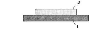
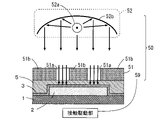
- FIG. 1 is a manufacturing process diagram for explaining a method of manufacturing a printed circuit board according to an embodiment of the present invention.
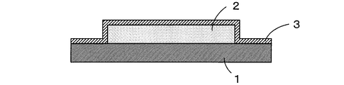
- FIG. 2 is a manufacturing process diagram for explaining a method of manufacturing a printed circuit board according to an embodiment of the present invention.
- FIG. 3 is a manufacturing process diagram for explaining a method of manufacturing a printed circuit board according to an embodiment of the present invention.
- FIG. 4 is a manufacturing process diagram for explaining a method of manufacturing a printed circuit board according to an embodiment of the present invention.
- FIG. 5 is a manufacturing process diagram for explaining a method of manufacturing a printed circuit board according to an embodiment of the present invention.
- FIG. 6 is a manufacturing process diagram for explaining a method of manufacturing a printed circuit board according to an embodiment of the present invention.
- FIG. 1 is a manufacturing process diagram for explaining a method of manufacturing a printed circuit board according to an embodiment of the present invention.
- FIG. 2 is a manufacturing process diagram for explaining a method of manufacturing a printed circuit board according to an embodiment of the present invention.
- FIG. 7 is a manufacturing process diagram for explaining a method of manufacturing a printed circuit board according to an embodiment of the present invention.
- FIG. 8 is a manufacturing process diagram for explaining a method of manufacturing a printed circuit board according to an embodiment of the present invention.
- FIG. 9 is a manufacturing process diagram for explaining a method of manufacturing a printed circuit board according to an embodiment of the present invention.
- FIG. 10 is a manufacturing process diagram for explaining a method of manufacturing a printed circuit board according to an embodiment of the present invention.
- FIG. 11 is a manufacturing process diagram for explaining a method of manufacturing a printed circuit board according to an embodiment of the present invention.
- FIG. 12 is a manufacturing process diagram for explaining a method of manufacturing a printed circuit board according to an embodiment of the present invention.
- FIG. 13 is a schematic diagram showing one configuration example of a roll-to-roll apparatus used in the method of manufacturing a printed circuit board.
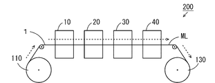
- FIG. 14 is a schematic diagram showing another configuration example of the roll-to-roll apparatus used in the method of manufacturing the printed circuit board.
- FIG. 15 is a schematic diagram showing another configuration example of the roll-to-roll apparatus used in the method of manufacturing the printed circuit board.
- a method for manufacturing a printed circuit board according to one embodiment of the present invention will be described below with reference to the drawings.
- a method of manufacturing a printed circuit board a method of manufacturing a flexible printed circuit board that can be applied to a semiconductor device or the like will be described.
- the flexible printed circuit board is abbreviated as printed circuit board.
- FIGS. 1 to 12 are manufacturing process diagrams for explaining a method for manufacturing a wired circuit board according to an embodiment of the present invention.
- a roll around which a long metal supporting substrate 1 is wound (hereinafter referred to as a delivery roll) is prepared, and the metal supporting substrate 1 is delivered from the prepared delivery roll.
- the metal supporting substrate 1 delivered from the delivery roll is wound around another roll (hereinafter referred to as a take-up roll).
- FIG. 1 shows a portion of the metal supporting substrate 1 unwound from the unwinding roll.
- a metal support substrate 1 according to the present embodiment is a support substrate made of stainless steel.
- the thickness of the metal supporting substrate 1 is preferably 10 ⁇ m or more and 100 ⁇ m or less, and is 20 ⁇ m in the present embodiment.
- the metal supporting board 1 is provided with the rigidity necessary for fabricating a printed circuit board by roll-to-roll.
- the thickness of the metal supporting substrate 1 is 100 ⁇ m or less, the flexibility necessary for roll-to-roll fabrication of the printed circuit board is ensured.
- an insulating layer 2 made of photosensitive polyimide is formed in a predetermined region on the upper surface of the metal supporting substrate 1 that has been drawn out.
- the thickness of the insulating layer 2 is 1 ⁇ m or more and 30 ⁇ m or less. Note that the insulating layer 2 may be formed so as to cover the entire upper surface of the metal supporting substrate 1 .
- a seed layer 3 is formed so as to cover the upper surface of the insulating layer 2, the side surfaces of the insulating layer 2, and the upper surface of the metal supporting board 1 where the insulating layer 2 is not formed.
- the seed layer 3 has a configuration in which a copper thin film is further laminated on an underlying layer in which two or more thin films selected from a chromium thin film, a nickel thin film, a titanium thin film, and an alloy thin film of chromium and nickel are laminated.
- the seed layer 3 may have a structure in which one of a chromium thin film, a nickel thin film, a titanium thin film, and a chromium-nickel alloy thin film is used as a base layer, and a copper thin film is laminated on the base layer. good.
- Each thin film forming the seed layer 3 is formed by, for example, sputtering or electroless plating.
- the seed layer 3 has a thickness of 0.01 ⁇ m or more and 1 ⁇ m or less.
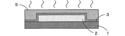
- the seed layer 3 is coated with a resist solution 4p. Thereby, a liquid film 4 of the resist liquid 4p is formed on the seed layer 3 .
- the application of the resist liquid 4 p onto the seed layer 3 is performed by a resist coating device 30 .
- the resist coating device 30 includes, for example, a coating nozzle 31 extending in a direction perpendicular to the conveying direction of the metal supporting substrate 1 (hereinafter referred to as a transverse direction).
- the coating nozzle 31 is provided at a position above the metal supporting substrate 1 conveyed between the feed roll and the take-up roll, and has a slit-shaped liquid discharge port 31s extending in the transverse direction.
- the coating nozzle 31 ejects the resist liquid 4p in a curtain shape toward the metal supporting substrate 1 conveyed from the slit-shaped liquid ejection port 31s.
- a positive photosensitive resin is used as the resist liquid 4p. More specifically, a positive photosensitive phenol resin or a positive acrylic resin is used as the resist liquid 4p.
- the amount of the resist liquid 4p supplied onto the metal supporting substrate 1 is adjusted so that the liquid film 4 is 1 ⁇ m or more and 15 ⁇ m or less.
- the resist liquid 4p contains a solvent component.
- the heat treatment removes the solvent component contained in the liquid film 4 to form a hardened resist layer 5 as shown in FIG.
- the thickness of the resist layer 5 is 1 ⁇ m or more and 5 ⁇ m or less.
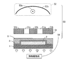
- the first exposure device 50 includes a mask 51 , a light source 52 and a contact driver 59 .
- the mask 51 has a light-transmitting portion 51a and a light-shielding portion 51b, and is arranged at a position above the metal supporting substrate 1 to be transported.
- light transmitting portions 51a are formed in a predetermined pattern.
- the light source 52 mainly consists of a lamp 52a and a mirror 52b, and is arranged to face the resist layer 5 with the mask 51 interposed therebetween.
- the lamp 52 a generates exposure light corresponding to the resist layer 5 .
- the mirror 52 b reflects the exposure light generated by the lamp 52 a toward the mask 51 .
- the metal supporting substrate 1 is covered with the mask 51 by the contact driving section 59 as indicated by the white arrow in FIG. pressed towards.
- the mask 51 is pressed toward the metal support substrate 1 by the contact driving portion 59 .
- a pressure greater than or equal to a predetermined pressure (pressing force) is applied between the resist layer 5 and the mask 51 .
- the contact drive unit 59 may have, for example, a lower surface contact member that contacts the lower surface of the metal supporting substrate 1 and an actuator that moves the lower surface contact member so that the metal supporting substrate 1 is pushed toward the mask 51. good.
- the contact driver 59 may have a top contact member that contacts the top surface of the mask 51 and an actuator that moves the top contact member so that the mask 51 is pushed toward the metal support substrate 1 .
- the contact driver 59 lowers the air pressure in the space surrounding the contact portion in a state where the lower surface of the mask 51 and the resist layer 5 are in contact with each other, thereby maintaining a predetermined pressure between the mask 51 and the resist layer 5 . (Crimping force) or more pressure may be applied.
- the predetermined pressure value may be set to a different value depending on the configuration of the contact driver 59 that brings the mask 51 and the resist layer 5 into contact.
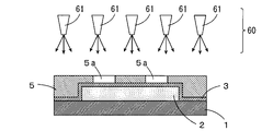
- the exposed resist layer 5 is developed.
- the resist layer 5 is developed by the first developing device 60 .
- the first developing device 60 includes multiple developing nozzles 61 .
- Each developing nozzle 61 is a spray nozzle arranged at a position above the transported metal supporting board 1 and sprays a developer toward the metal supporting board 1 .
- the resist layer 5 is composed of a positive photosensitive resin
- the exposed portion is dissolved in the developer and removed.
- openings 5 a having a predetermined pattern are formed in the resist layer 5 .
- the seed layer 3 is exposed upward in the opening 5a.
- the pattern width of the openings 5a in a cross section perpendicular to the one direction is 1 ⁇ m or more and 6 ⁇ m or less.
- a conductor layer 6 having a predetermined pattern is formed on the portion of the seed layer 3 exposed in the opening 5a (FIG. 8) of the resist layer 5 by electroplating.
- the thickness of the conductor layer 6 is 1 ⁇ m or more and 6 ⁇ m or less.
- the pattern width of the conductor layers 6 in a cross section orthogonal to the one direction is 1 ⁇ m or more and 5 ⁇ m or less.
- a second exposure device 80 includes a light source 81 and does not have a mask.
- the light source 81 like the light source 52, mainly consists of a lamp 81a and a mirror 81b.
- the second exposure device 80 may be provided with a transparent mask, that is, a mask consisting only of the light-transmitting portions 51a without the light-shielding portions 51b.
- the energy of the exposure light applied per unit area of the target when the target is exposed is called the exposure amount.
- the unit of exposure dose is represented by, for example, “mJ/cm 2 ”.
- the exposure amount of the resist layer 5 is the integrated light amount of the exposure light irradiated toward the resist layer 5 from the second exposure device 80, and the illuminance of the exposure light irradiated toward the resist layer 5 and the resist layer 5 It is determined by the irradiation time of the exposure light. Therefore, when the second exposure device 80 irradiates the resist film 5 with exposure light at a constant illuminance, the exposure amount of the resist layer 5 can be easily adjusted by adjusting the irradiation time.
- the exposure amount of the resist layer 5 is 5 mJ/cm 2 or more.
- the exposure amount of the resist layer 5 is preferably 100 mJ/cm 2 or more, more preferably 500 mJ/cm 2 or more.
- the exposed resist layer 5 is developed. Development of the resist layer 5 is performed by a second developing device 90 .
- the second developing device 90 includes a plurality of developing nozzles 91 like the first developing device 60 .
- Each developing nozzle 91 is a spray nozzle arranged at a position above the transported metal supporting board 1 and sprays a developer toward the metal supporting board 1 .
- the resist layer 5 is composed of a positive photosensitive resin
- the entire resist layer 5 is dissolved in the developer and removed.
- portions of the seed layer 3 where the conductor layer 6 is not formed are exposed.
- the exposed unnecessary portions of the seed layer 3 are removed by wet etching, for example.
- the laminated body of the metal supporting board 1, the insulating layer 2, the seed layer 3 and the conductor layer 6 is completed as the wired circuit board 7.
- the seed layer 3 and the conductor layer 6 formed in a predetermined pattern on the insulating layer 2 constitute the wiring of the printed circuit board 7 .
- the completed wired circuit board 7 is wound up on a winding roll.
- FIG. 13 is a schematic diagram showing one configuration example of a roll-to-roll apparatus used in the method of manufacturing a printed circuit board.
- the roll-to-roll apparatus 100 of FIG. 13 includes a delivery roll 110, an insulating layer forming apparatus 10, a seed layer forming apparatus 20, a resist coating apparatus 30, a heat treatment apparatus 40, a first exposure apparatus 50, a first developing apparatus 60, a plating It includes apparatus 70 , second exposure apparatus 80 , second development apparatus 90 , etching apparatus 95 and take-up roll 120 .
- a long metal support substrate 1 (FIG. 1) is wound around a bobbin (not shown).
- the metal supporting substrate 1 is delivered from the delivery roll 110 by rotating the delivery roll 110 .
- the fed metal supporting substrate 1 is sent to the insulating layer forming apparatus 10 .
- FIG. 13 the conveying direction of the metal supporting substrate 1 delivered from the delivery roll 110 is indicated by a dotted arrow.
- the insulating layer forming apparatus 10 forms the insulating layer 2 on the metal supporting substrate 1 as shown in the example of FIG.
- the metal supporting substrate 1 with the insulating layer 2 formed thereon is sent to the seed layer forming apparatus 20 .
- the seed layer forming apparatus 20 forms a seed layer 3 on the metal supporting substrate 1 so as to cover the insulating layer 2, as shown in the example of FIG.
- a laminate consisting of the metal supporting substrate 1 , the insulating layer 2 and the seed layer 3 is sent to a resist coating device 30 .
- the resist coating device 30 is equipped with a coating nozzle 31 and forms a liquid film 4 of a resist liquid 4p on the seed layer 3 .
- the laminate with the liquid film 4 formed thereon is sent to a heat treatment device 40 .
- the heat treatment device 40 includes, for example, a heater, and heats the liquid film 4 (FIG. 4) of the resist solution 4p.
- a resist layer 5 is formed on the seed layer 3 as shown in the example of FIG.
- the laminate with the resist layer 5 formed thereon is sent to the first exposure device 50 .
- the first exposure device 50 includes a mask 51, a light source 52, and a contact driver 59, as shown in the examples of FIGS.
- the first exposure device 50 exposes the resist layer 5 in a predetermined pattern while bringing the resist layer 5 and mask 51 into contact with each other.
- the laminate having the resist layer 5 exposed in a predetermined pattern is sent to the first developing device 60 .
- the first developing device 60 includes a plurality of developing nozzles 61, and supplies developer from the plurality of developing nozzles 61 onto the resist layer 5 after exposure. As a result, the exposed portions of the resist layer 5 are removed by the developer, and openings 5a having a predetermined pattern are formed in the resist layer 5. Next, as shown in FIG. The laminate including the resist layer 5 after development is sent to the plating apparatus 70 .
- the plating apparatus 70 forms the conductor layer 6 in the opening 5a (FIG. 8) of the resist layer 5 by electroplating, as shown in the example of FIG.
- the laminate on which the conductor layer 6 of the predetermined pattern is formed is sent to the second exposure device 80 .
- the second exposure device 80 has a light source 81 as shown in the example of FIG.
- the second exposure device 80 exposes the entire surface of the resist layer 5 .
- the laminate with the entire resist layer 5 exposed is sent to the second developing device 90 .
- the second developing device 90 has a plurality of developing nozzles 91, and supplies developer from the plurality of developing nozzles 91 onto the resist layer 5 after exposure. As a result, the entire exposed resist layer 5 is removed by the developer. The laminate from which the resist layer 5 has been removed is sent to an etching device 95 .
- the etching device 95 removes the exposed portion of the seed layer 3 by wet etching, for example, as shown in the example of FIG. As a result, the seed layer 3 and the conductor layer 6 existing on the insulating layer 2 are formed as wiring, and the wired circuit board 7 is completed.
- the printed circuit board 7 completed in the etching device 95 is wound around the winding roll 120 .
- the printed circuit board 7 may be manufactured using the following roll-to-roll apparatus instead of the roll-to-roll apparatus 100 shown in FIG. good.
- 14 and 15 are schematic diagrams showing another configuration example of the roll-to-roll apparatus used in the method of manufacturing the printed circuit board.
- two roll-to-roll devices 200 and 300 are used instead of the roll-to-roll device 100 of FIG.
- substantially the first half of the series of steps for manufacturing the printed circuit board 7 is performed.
- the roll-to-roll apparatus 300 of FIG. 15 substantially the latter half of the series of steps for manufacturing the printed circuit board 7 is performed.
- the roll-to-roll apparatus 200 in FIG. 14 includes a delivery roll 110, an insulating layer forming apparatus 10, a seed layer forming apparatus 20, a resist coating apparatus 30, a heat treatment apparatus 40, and an intermediate take-up roll .
- the metal supporting substrate 1 delivered from the delivery roll 110 is sent to the insulating layer forming apparatus 10, the seed layer forming apparatus 20, the resist coating apparatus 30 and the heat treatment apparatus 40 in sequence.
- the conveying direction of the metal supporting substrate 1 delivered from the delivery roll 110 is indicated by a dotted arrow.
- the insulating layer forming apparatus 10, the seed layer forming apparatus 20, the resist coating apparatus 30, and the heat treatment apparatus 40 in FIG. 14 have the same configurations as the components denoted by the same reference numerals in FIG. Thereby, an insulating layer 2 , a seed layer 3 and a resist layer 5 are sequentially formed on the metal supporting substrate 1 .
- the laminate ML after the formation of the resist layer 5 by the heat treatment device 40 is taken up by the intermediate take-up roll 130 .
- a roll-to-roll apparatus 300 in FIG. and take-up roll 120 As the intermediate delivery roll 140, the intermediate take-up roll 130 of the roll-to-roll device 200 of FIG. 14 is prepared.
- the laminate ML delivered from the intermediate delivery roll 140 passes through the first exposure device 50, the first development device 60, the plating device 70, the second exposure device 80, and the second development device 90. and sequentially sent to the etching device 95 .
- the conveying direction of the laminate ML delivered from the intermediate delivery roll 140 is indicated by a dotted arrow.
- the first exposure device 50, the first development device 60, the plating device 70, the second exposure device 80, the second development device 90 and the etching device 95 in FIG. 15 are denoted by the same reference numerals in FIG. Each element has the same configuration.
- the resist layer 5 formed on the metal supporting substrate 1 is exposed in a predetermined pattern and developed.
- the conductor layer 6 is formed in the opening 5a of the resist layer 5 formed by development.
- the entire surface of the resist layer 5 is exposed and developed.
- the exposed seed layer 3 is removed.
- the wiring circuit board 7 from which the seed layer 3 has been removed by the etching device 95 is taken up by the take-up roll 120 .
- the resist layer 5 is formed by applying a resist liquid 4p onto the insulating layer 2 and heat-treating the liquid film 4 of the applied resist liquid 4p.
- the thickness of the liquid film 4 formed on the insulating layer 2 can be reduced by adjusting the amount of the resist liquid 4p supplied onto the insulating layer.
- the thickness of the resist layer 5 can be made sufficiently smaller than that of a resist layer formed using a dry film resist. When the thickness of the resist layer 5 is small, it becomes possible to form the openings 5a in the resist layer 5 with a finer pattern.
- a support substrate made of stainless steel is used as the metal support substrate 1 .
- Metal support substrate 1 made of stainless steel has relatively high rigidity.
- the metal supporting board 1 made of stainless steel has higher rigidity than the metal supporting board made of copper.
- stainless steel has a relatively low thermal conductivity as a metallic material.
- a metal support substrate 1 made of stainless steel has a lower thermal conductivity than a metal support substrate made of copper.
- the resist layer 5 is made of a positive photosensitive resin. After forming the conductor layer 6, the entire resist layer 5 is exposed and developed. Therefore, after the conductor layer 6 is formed in the openings 5a of the resist layer 5, the portions of the resist layer 5 adjacent to the conductor layer 6 are dissolved in the developer (alkaline solution). Thereby, the unnecessary resist layer 5 can be easily removed from the metal supporting board 1 after the conductor layer 6 is formed. As a result, part of the resist layer 5 is prevented from remaining as a foreign matter on the printed circuit board 7 produced. In addition, defective removal of the seed layer 3 due to a portion of the resist layer 5 remaining can be prevented. Therefore, occurrence of a short circuit between a plurality of wirings on the printed circuit board 7 is prevented.
- the insulating layer 2 is made of photosensitive polyimide.
- the thickness of the insulating layer 2 can be reduced by forming the insulating layer 2 using a photolithographic technique. Moreover, it becomes possible to easily form the insulating layer 2 in a desired pattern.
- the surface of the insulating layer 2 can be mirror-finished without requiring mechanical or chemical processing. When the surface of the insulating layer 2 is mirror-finished, scattering of the exposure light incident on the insulating layer 2 on the surface of the insulating layer 2 is suppressed when the resist layer 5 is exposed. Thereby, it becomes possible to form the openings 5a in the resist layer 5 with a finer pattern.
- a plurality of processes for forming the printed circuit board 7 are performed by one roll-to-roll machine 100 or two roll-to-roll machines 200 and 300. Although steps are performed, the invention is not limited thereto. A plurality of processing steps for forming the printed circuit board 7 may be performed using three or more roll-to-roll machines. Alternatively, each of the multiple processing steps for forming the printed circuit board 7 may be performed using separate roll-to-roll equipment.
- the delivery roll 110 around which the elongated metal supporting substrate 1 is wound is prepared, but the present invention is not limited to this.
- a two-layer substrate roll in which the metal supporting substrate 1 and the insulating layer 2 are laminated may be prepared as the pay-out roll 110 .
- the step of forming the insulating layer 2 on the metal supporting substrate 1 (FIG. 2) can be omitted.
- the resist layer 5 is pressed against the lower surface of the mask 51 with a predetermined force during the exposure for forming the openings 5a of the predetermined pattern in the resist layer 5.
- the invention is not limited to these examples. During the exposure for forming the openings 5a of the predetermined pattern in the resist layer 5, the resist layer 5 and the mask 51 may be kept separated from each other.
- resist layer 5 and mask 51 are kept in contact with each other at a pressure lower than the predetermined pressure in the above embodiment. good too.
- the process of exposing while bringing the resist layer 5 and the mask 51 into contact with each other and applying a pressure lower than a predetermined value between the resist layer 5 and the mask 51 is called soft contact exposure.
- a positive photosensitive phenolic resin or a positive acrylic resin is used as the material of the resist layer 5, but the present invention is not limited to this.
- a positive epoxy resin may be used, or a positive photosensitive polyimide may be used.
- a positive photosensitive resin is used as the material of the resist layer 5, but the present invention is not limited to this.
- a negative photosensitive resin may be used instead of the positive photosensitive resin.
- the resist layer 5 is removed using, for example, a solvent or a remover containing the same components as the developer for the photosensitive resin. As a result, the process of exposing and developing the entire resist layer 5 becomes unnecessary.
- a support substrate made of stainless steel is used as the metal support substrate 1, but the present invention is not limited to this.
- a supporting substrate made of stainless steel instead of the supporting substrate made of stainless steel, a supporting substrate made of copper, a supporting substrate made of nickel, a supporting substrate made of a copper alloy, or the like can be used.
- the seed layer 3 is formed on the insulating layer 2 in order to form the conductor layer 6 by electroplating, but the present invention is not limited to this. If the conductor layer 6 is formed by, for example, electroless plating, the seed layer 3 may not be formed.
- photosensitive polyimide is used as the material of the insulating layer 2, but the present invention is not limited to this.
- a resin other than photosensitive polyimide phenol resin, acrylic resin, epoxy resin, etc.
- the resist layer 5 formed on the seed layer 3 in the above embodiment is removed without exposure and development by using a stripping solution containing the same components as the developer for the photosensitive resin. is also possible. Therefore, after the conductor layer 6 is formed, the unnecessary resist layer 5 may be removed using a stripping solution instead of performing the entire surface exposure and development on the resist layer 5 .
- the time required to dissolve the resist layer 5 is longer than when the resist layer 5 is removed by whole-surface exposure and development. Also, in this case, it is necessary to maintain the processing environment at a temperature higher than room temperature (for example, about 40° C. to 50° C.) in order to promote and stabilize the reaction between the resist layer 5 and the stripping solution. Therefore, the previously formed conductor layer 6 may be oxidized by the remover, and the electrical characteristics of the wiring may be degraded. Therefore, the resist layer 5 is preferably removed by exposure and development as shown in the above embodiment.
- the wired circuit board 7 is an example of a wired circuit board
- the metal supporting board 1 is an example of a metal supporting board
- the insulating layer 2 is an example of an insulating layer
- the resist layer 5 is a plating resist.
- layers are examples of layers.
- the opening 5a is an example of an opening
- the conductor layer 6 is an example of a conductor layer
- the mask 51 is an example of a mask
- the seed layer 3 is an example of a seed layer.
- Various other elements having the structure or function described in the claims can be used as each component of the claims.
- test masks used to fabricate the printed circuit boards of Example 1 and Comparative Examples 1 to 4 had 1 ⁇ m/1 ⁇ m, 2 ⁇ m/2 ⁇ m, 3 ⁇ m/3 ⁇ m, 4 ⁇ m/4 ⁇ m, 5 ⁇ m/5 ⁇ m, 6 ⁇ m 9 ⁇ m/6 ⁇ m, 7 ⁇ m/7 ⁇ m, 8 ⁇ m/8 ⁇ m and 9 ⁇ m/9 ⁇ m corresponding to 9 L/S patterns are formed in the light projecting portion.
- the present inventors compared the minimum L/S at which wiring could be formed for the wired circuit boards of Example 1 and Comparative Examples 1-4.
- the wired circuit board of Example 1 was manufactured according to the method of manufacturing the wired circuit board according to the above embodiment (see FIGS. 1 to 12). Specifically, when manufacturing the wired circuit board of Example 1, an insulating layer 2 made of photosensitive polyimide was formed on a metal supporting board 1 , and a seed layer 3 was further formed on the insulating layer 2 . Further, a resist layer 5 made of a positive photosensitive resin was formed on the seed layer 3 by coating the seed layer 3 with the resist solution 4p and performing heat treatment. The thickness of the resist layer 5 was 3 ⁇ m. When exposing the resist layer 5, hard contact exposure was performed using the above test mask. In this hard contact exposure, the metal supporting substrate 1 was pressed against the mask 51 so that a pressure of 0.5 MPa was applied between the resist layer 5 and the mask 51 .
- the wired circuit board of Comparative Example 1 was manufactured by the same method as the manufacturing method of the wired circuit board of Example 1 above, except for the following points.
- the resist layer 5 was formed by sticking a dry film resist onto the seed layer 3 .
- the resist layer 5 was made of a negative photosensitive resin and had a thickness of 10 ⁇ m. Further, when the wired circuit board of Comparative Example 1 was produced, the film-like resist layer 5 was peeled off from the seed layer 3 after the conductive layer 6 was formed.
- wiring with L/S of 6 ⁇ m/6 ⁇ m to 9 ⁇ m/9 ⁇ m was formed.
- the wired circuit board of Comparative Example 2 was produced in the same manner as the wired circuit board of Comparative Example 1 except that the thickness of the dry film resist used was changed.
- the thickness of the resist layer 5 formed on the seed layer 3 was 15 ⁇ m.
- wiring with L/S of 8 ⁇ m/8 ⁇ m to 9 ⁇ m/9 ⁇ m was formed.
- no wiring with an L/S of 1 ⁇ m/1 ⁇ m to 7 ⁇ m/7 ⁇ m was formed. That is, for the wired circuit board of Comparative Example 2, the minimum L/S at which wiring could be formed was 8 ⁇ m/8 ⁇ m.
- the thickness of the wiring formed on the printed circuit board of Comparative Example 2 was 8 ⁇ m.
- the wired circuit board of Comparative Example 3 was manufactured in the same manner as the wired circuit board of Comparative Example 1 except that the exposure method of the resist layer 5 was changed.
- the resist layer 5 is exposed in a predetermined pattern during the production of the printed circuit board of Comparative Example 3, the resist layer 5 is exposed from the exposure apparatus while the resist layer 5 and the test mask are separated from each other by a minute distance.
- a process of irradiating with light was performed.
- Such exposure processing is called proximity exposure.
- proximity exposure the distance between the resist layer 5 and the mask (in this example, the test mask) is maintained at, for example, several tens of micrometers.
- the wired circuit board of Comparative Example 4 was produced in the same manner as the wired circuit board of Comparative Example 3 except that the thickness of the dry film resist used was changed.
- the thickness of the resist layer 5 formed on the seed layer 3 was 20 ⁇ m.
- wiring with L/S of 6 ⁇ m/6 ⁇ m to 9 ⁇ m/9 ⁇ m was formed.
- no wiring with an L/S of 1 ⁇ m/1 ⁇ m to 5 ⁇ m/5 ⁇ m was formed. That is, for the wired circuit board of Comparative Example 4, the minimum L/S at which wiring could be formed was 6 ⁇ m/6 ⁇ m.
- the thickness of the wiring formed on the printed circuit board of Comparative Example 4 was 6 ⁇ m.
- the thickness (3 ⁇ m) of the resist layer 5 formed on the wired circuit board of Example 1 is equal to the thickness (10 ⁇ m to 20 ⁇ m) of the resist layer 5 formed on the wired circuit boards of Comparative Examples 1 to 4. small enough compared to As a result, it can be seen that when the resist liquid 4p is applied and the heat treatment is performed, the resist layer 5 having a sufficiently small thickness can be formed as compared with the case where the existing dry film resist is used.
- the minimum L/S (2 ⁇ m/2 ⁇ m) of Example 1 was the minimum L/S (6 ⁇ m/6 ⁇ m) of Comparative Example 1, It is sufficiently smaller than the minimum L/S of Comparative Example 2 (8 ⁇ m/8 ⁇ m), the minimum L/S of Comparative Example 3 (6 ⁇ m/6 ⁇ m) and the minimum L/S of Comparative Example 4 (6 ⁇ m/6 ⁇ m).
- the unnecessary resist layer 5 after the formation of the conductor layer 6 may be removed by exposing and developing the entire surface, or the entire surface may be exposed. It may be removed using a stripping solution without exposure and development.
- the present inventors conducted Examples 1 to 6 and Comparative Example 1, in which the manufacturing methods are different from each other, in order to confirm the peeling ability according to the removal method and removal conditions for the unnecessary resist layer 5 after the formation of the conductor layer 6. 4 wiring circuit boards were produced.
- the wired circuit board of Example 1 used in this verification test is the same as the wired circuit board of Example 1 produced in the line and space verification test. As described above, the wired circuit board of Example 1 was produced according to the method for manufacturing a wired circuit board shown in FIGS.
- the exposure amount of the resist layer 5 was set to 2000 mJ/cm 2 in the entire surface exposure for removing the unnecessary resist layer 5 after the formation of the conductor layer 6 .
- an ultraviolet irradiator model UV-2001M-ND
- Sanei Electric Works Co., Ltd. was used.
- the energy of the exposure light (ultraviolet rays including at least part of g-line, h-line and i-line) irradiated per unit area and per unit time to the resist layer 5 from the ultraviolet irradiator (Illuminance) was 90 mJ/cm 2 .
- a developer (P-10) manufactured by Tokyo Ohka Kogyo Co., Ltd. was used during development for removing the unnecessary resist layer 5 after the formation of the conductor layer 6. board. This development was carried out by setting the temperature environment to 25° C. and setting the development time to 100 seconds.
- the wired circuit boards of Examples 2 to 5 used in this confirmation test were produced in the same manner as the wired circuit board of Example 1, except that the exposure amount of the resist layer 5 when the entire surface of the resist layer 5 was exposed was different. did. Specifically, in the wiring circuit board of Example 2, the exposure amount of the resist layer 5 during the entire surface exposure was set to 5 mJ/cm 2 . In the wiring circuit board of Example 3, the exposure amount of the resist layer 5 during the entire surface exposure was set to 100 mJ/cm 2 . In the wiring circuit board of Example 4, the exposure amount of the resist layer 5 during the entire surface exposure was set to 500 mJ/cm 2 . In the printed circuit board of Example 5, the exposure amount of the resist layer 5 during the entire surface exposure was set to 1000 mJ/cm 2 .
- the wiring circuit board of Example 6 used in this confirmation test was the same as that of Example 6, except that the unnecessary resist layer 5 after the formation of the conductor layer 6 was removed using a stripping solution without performing the entire surface exposure and development. It was produced in the same manner as the wiring circuit board of No. 1.
- the wired circuit boards of Comparative Examples 1 to 4 used in this verification test are the same as the wired circuit boards of Comparative Examples 1 to 4 produced in the line and space verification test.
- the resist layer 5 was formed using a dry film resist.
- the unnecessary resist layer 5 after the formation of the conductor layer 6 was removed by physically peeling it off from the seed layer 3 .
- the unnecessary resist layer 5 after the formation of the conductor layer 6 was not subjected to overall exposure and development.
- a portion of the resist layer 5 remaining on the plurality of wirings and their peripheral portions is called a resist residue.
- the present inventors examined the wiring circuit boards of Examples 1 to 6 and Comparative Examples 1 to 4 produced as described above using an SEM (scanning electron microscope) at an acceleration voltage of 15 kV and a magnification of 1500 times. A secondary electron image was acquired at , and the presence or absence of resist residue was confirmed. As a result, no resist residue was observed in the printed circuit boards of Examples 1 to 5. On the other hand, the wiring circuit boards of Example 6 and Comparative Examples 1 to 4 were found to have residual resist.
- the present inventors confirmed the presence or absence of resist residues on the wiring circuit boards of Examples 1 to 6 and Comparative Examples 1 to 4 produced as described above with an optical microscope at a magnification of 20 times. As a result, no resist residue was found in the printed circuit boards of Examples 1 to 6. On the other hand, the printed circuit boards of Comparative Examples 1 to 4 were found to have residual resist.
- the inventors of the present invention confirmed that the wiring circuit boards of Examples 1 to 6 and Comparative Examples 1 to 4, as a comprehensive confirmation result of the resist residue, from the confirmation results of each wiring circuit board by SEM and optical microscope.
- Generation levels A, B, and C of residues were determined.
- the generation level A of resist residue indicates that no resist residue was observed in both the results of confirmation by SEM and optical microscope.
- the generation level B of resist residue indicates that no resist residue was observed only in either one of the confirmation results by SEM and optical microscope.
- the generation level C of the resist residue indicates that the resist residue was observed both in the results of confirmation by SEM and optical microscope.
- the resist residue generation level of the printed circuit boards of Examples 1 to 5 is A.
- the printed circuit boards of Example 6 and Comparative Example 4 have a resist residue generation level of B.
- the printed circuit boards of Comparative Examples 1 to 3 have a resist residue generation level of C.
- FIG. Table 2 below shows the confirmation test results regarding the peeling of the resist layer. Table 2 below shows the test results as well as whether or not the entire surface was exposed to light when removing the unnecessary resist layer 5 after the formation of the conductor layer 6, and the amount of exposure during the entire surface exposure.
- the wiring circuits of Examples 1 to 5 obtained by exposing the entire surface of the unnecessary resist layer 5 of the wiring circuit boards of Examples 1 to 6 to an exposure amount of 5 mJ/cm 2 or more and developing the wiring circuits. No resist residue was observed on the substrate.
- the wiring circuit board of Example 6 in which the unnecessary resist layer 5 was removed by the stripping solution without exposing and developing the entire surface, generated a resist residue by SEM. was accepted.
- the wiring circuit boards of Comparative Examples 1 to 4 in which the unnecessary resist layer 5 was removed by peeling off the dry film resist generation of resist residue was observed at least by SEM. Therefore, in order to suppress the generation of resist residue, it is preferable to expose the entire surface of the unnecessary resist layer 5 with an exposure amount of 5 mJ/cm 2 or more and develop it.
Landscapes
- Engineering & Computer Science (AREA)
- Manufacturing & Machinery (AREA)
- Microelectronics & Electronic Packaging (AREA)
- Manufacturing Of Printed Wiring (AREA)
Abstract
配線回路基板の製造方法は、ロールツーロールにより長尺状の金属支持基板上に絶縁層を形成する工程と、ロールツーロールにより絶縁層上に感光性材料を含むめっきレジスト層を形成する工程とを含む。また、配線回路基板の製造方法は、ロールツーロールによりめっきレジスト層を所定パターンで露光する工程と、ロールツーロールにより所定パターンで露光されためっきレジスト層を現像することにより、めっきレジスト層に所定パターンまたは所定パターンとは逆パターンの開口を形成する工程と、ロールツーロールにより開口内に導体層を形成する工程とを含む。めっきレジスト層を形成する工程は、絶縁層上に感光性のレジスト液を塗布し、塗布されたレジスト液の液膜に熱処理を施すことを含む。
Description
本発明は、配線回路基板の製造方法に関する。
従来より、フレキシブル配線回路基板等の配線回路基板の製造方法においては、ロールツーロールが多く利用されている。ロールツーロールにおいては、例えば長尺状の支持基板が巻回されたロールが用意される。用意されたロールから支持基板が繰り出される。繰り出された支持基板に所定の処理が施され、処理後の支持基板がロール状に巻き取られる(例えば、特許文献1参照)。
特許文献1に記載された回路付きサスペンション基板の製造方法においては、上記の所定の処理として、支持基板上にベース絶縁層、クロム薄膜および銅薄膜がこの順で形成される。また、ドライフィルムレジストを用いて銅薄膜上にめっきレジストが形成される。めっきレジストは、所定パターンと逆パターンの開口を有する。さらに、めっきレジストが形成されていない部分で露出する銅薄膜上に、所定パターンの導体層が配線として形成される。その後、めっきレジストと、導体層が形成されていない部分の銅薄膜が除去される。
ロールツーロールによれば、上記の一連の処理の一部または全てを連続的に行うことが可能になる。それにより、配線回路基板の生産効率が向上し、生産コストの低減が実現される。
近年、フレキシブル配線回路基板の用途の多様化に伴い、導体パターンの微細化が求められている。しかしながら、特許文献1に記載された製造方法では、導体パターンの微細化に限界があった。
本発明の目的は、微細な導体パターンを有する配線回路基板を高い生産効率で製造することが可能な配線回路基板の製造方法を提供することである。
上記のように、支持基板および絶縁層上にめっきレジストを形成するために、ドライフィルムレジストが用いられる。ドライフィルムレジストは、感光性材料からなるフィルムと保護フィルムとが積層された構造を有し、支持基板および絶縁層上に容易に貼り付けることが可能である。支持基板および絶縁層上に貼り付けられたドライフィルムレジストが、露光および現像される。それにより、所定パターンの開口を有するめっきレジストが形成される。
導体パターンの微細化を実現するためには、めっきレジストにおける開口のパターンをより微細化する必要がある。開口のパターンをより微細化するためには、めっきレジストの厚みを小さくすること、すなわちドライフィルムレジストが薄型化されることが望ましい。しかしながら、ロールツーロールに用いるために必要な強度等を考慮すると、ドライフィルムレジストの薄型化には限界がある。本発明者らは、上記の点に着目し、以下に示す発明を案出した。
(1)本発明の一局面に従う配線回路基板の製造方法は、長尺状の金属支持基板上に絶縁層が形成された積層体を用意する工程と、ロールツーロールにより絶縁層上に感光性材料を含むめっきレジスト層を形成する工程と、ロールツーロールによりめっきレジスト層を所定パターンで露光する工程と、ロールツーロールにより所定パターンで露光されためっきレジスト層を現像することにより、めっきレジスト層に所定パターンまたは所定パターンとは逆パターンの開口を形成する工程と、ロールツーロールにより開口内に導体層を形成する工程とを含み、めっきレジスト層を形成する工程は、絶縁層上に感光性のめっきレジスト液を塗布し、塗布されためっきレジスト液に熱処理を施すことを含む。
その配線回路基板の製造方法においては、めっきレジスト層を形成する工程、めっきレジスト層を所定パターンで露光する工程、めっきレジスト層に開口を形成する工程、導体層を形成する工程が、それぞれロールツーロールにより行われる。それにより、高い生産効率で配線回路基板を製造することができる。
また、めっきレジスト層は、絶縁層上にめっきレジスト液を塗布し、塗布されためっきレジスト液に熱処理を施すことにより形成される。ここで、絶縁層上へのめっきレジスト液の供給量を調整することにより、絶縁層上に形成されるめっきレジスト液の液膜の厚みを小さくすることができる。この場合、ドライフィルムレジストを用いて形成されるめっきレジスト層に比べて、めっきレジスト層の厚みを十分小さくすることができる。めっきレジスト層の厚みが小さいと、当該めっきレジスト層に、より微細なパターンで開口を形成することが可能になる。
これらの結果、微細な導体パターンを有する配線回路基板を高い生産効率で製造することが可能になる。
(2)めっきレジスト層を所定パターンで露光する工程は、所定パターンに対応するマスクとめっきレジスト層とを互いに接触させつつ、マスクを通してめっきレジスト層に露光光を照射する接触露光を行うことを含んでもよい。
この場合、マスクとめっきレジスト層とが接触することにより、マスクとめっきレジスト層との位置関係が固定される。また、マスクとめっきレジスト層との間に隙間(空間)が形成されないので、露光光の広がりが抑制される。これらの結果、より高い精度で微細なパターンの露光が可能となる。
(3)接触露光は、マスクとめっきレジスト層とが互いに接触した状態で、マスクとめっきレジスト層との間に予め定められた圧力以上の圧力を作用させることを含んでもよい。これにより、さらに高い精度で微細なパターンの露光が可能となる。
(4)金属支持基板は、ステンレス鋼からなってもよい。ステンレス鋼からなる金属支持基板は、例えば銅からなる金属支持基板に比べて高い剛性を有する。それにより、ロールツーロールにおいて、繰り出し用のロールと巻き取り用のロールとの間に位置する金属支持基板の部分にうねりが発生することが低減される。したがって、搬送中の金属支持基板の形状が平坦に維持されやすい。この場合、金属支持基板上に形成されるめっきレジスト層の厚みにばらつきが生じにくいので、高い精度で微細なパターンの露光が可能となる。また、金属支持基板の変形に伴ってめっきレジスト層に形成される開口のパターンが変形することが低減される。
さらに、ステンレス鋼は、金属材料として比較的低い熱伝導率を有する。例えば、ステンレス鋼からなる金属支持基板は、銅からなる金属支持基板に比べて低い熱伝導率を有する。これにより、めっきレジスト液に熱処理を施す場合には、金属支持基板により、めっきレジスト液の温度が急峻に上昇することが抑制される。それにより、めっきレジスト液の溶剤成分が適切に除去される。
(5)めっきレジスト液は、ポジ型の感光性樹脂からなり、配線回路基板の製造方法は、導体層を形成する工程の後、ロールツーロールによりめっきレジスト層の全体を露光する工程と、ロールツーロールにより全体が露光されためっきレジスト層を現像することにより、絶縁層上のめっきレジスト層を除去する工程とをさらに含んでもよい。
この場合、導体層と隣り合うように形成されためっきレジスト層の全体が、現像液に溶解する。したがって、導体層形成後の金属支持基板上から、不要なめっきレジスト層を容易に除去することができる。それにより、作製された配線回路基板にめっきレジスト層の一部が異物として残留することが防止される。
(6)導体層を形成する工程の後、めっきレジスト層の全体を露光する工程において、めっきレジスト層の露光量は5mJ/cm2以上であってもよい。この場合、露光後のめっきレジスト層に現像液を供給することにより、絶縁層上のめっきレジスト層が現像液に円滑に溶解する。それにより、導体層からなる複数の微細な配線間にめっきレジスト層が存在する場合でも、導体層を損傷させることなくそれらのめっきレジスト層が短時間で円滑に除去される。
(7)絶縁層は、感光性ポリイミドからなってもよい。この場合、フォトリソグラフィ技術を用いて絶縁層を形成することにより、絶縁層の薄膜化が可能になる。また、絶縁層を所望のパターンに容易に形成することが可能になる。さらに、絶縁層を感光性ポリイミドにより形成する場合には、機械的または化学的な加工を要することなく、絶縁層の表面を鏡面状態にすることができる。絶縁層の表面が鏡面状態にある場合、めっきレジスト層の露光時に、絶縁層に入射する露光光が絶縁層の表面で散乱することが抑制される。それにより、めっきレジスト層に、さらに微細なパターンで開口を形成することが可能になる。
(8)積層体を用意する工程の後、めっきレジスト層を形成する工程の前に、ロールツーロールにより絶縁層上にシード層を形成する工程をさらに含み、めっきレジスト層を形成する工程において、めっきレジスト層は、シード層を介して絶縁層上に形成され、導体層を形成する工程は、開口部内で露出するシード層上に電解めっきにより導体層を形成することを含んでもよい。この場合、導体層を電解めっきにより形成することができる。
本発明によれば、微細な導体パターンを有する配線回路基板を高い生産効率で製造することが可能になる。
以下、本発明の一実施の形態に係る配線回路基板の製造方法について図面を参照しつつ説明する。配線回路基板の製造方法の一例として、半導体装置等に適用可能なフレキシブル配線回路基板の製造方法を説明する。なお、以下の説明では、フレキシブル配線回路基板を配線回路基板と略記する。
[1]配線回路基板の製造方法
図1~図12は、本発明の一実施の形態に係る配線回路基板の製造方法を説明するための製造工程図である。まず、長尺状の金属支持基板1が巻回されたロール(以下、繰り出しロールと呼ぶ。)を用意し、用意した繰り出しロールから金属支持基板1を繰り出す。繰り出しロールから繰り出された金属支持基板1は、他のロール(以下、巻き取りロールと呼ぶ。)に巻き取られる。図1では、繰り出しロールから繰り出された金属支持基板1の一部が示される。本実施の形態に係る金属支持基板1は、ステンレス鋼からなる支持基板である。
図1~図12は、本発明の一実施の形態に係る配線回路基板の製造方法を説明するための製造工程図である。まず、長尺状の金属支持基板1が巻回されたロール(以下、繰り出しロールと呼ぶ。)を用意し、用意した繰り出しロールから金属支持基板1を繰り出す。繰り出しロールから繰り出された金属支持基板1は、他のロール(以下、巻き取りロールと呼ぶ。)に巻き取られる。図1では、繰り出しロールから繰り出された金属支持基板1の一部が示される。本実施の形態に係る金属支持基板1は、ステンレス鋼からなる支持基板である。
金属支持基板1の厚みは、10μm以上100μm以下であることが好ましく、本実施の形態では20μmである。金属支持基板1の厚みが10μm以上であることにより、金属支持基板1において、ロールツーロールによる配線回路基板の作製に必要な剛性が確保される。金属支持基板1の厚みが100μm以下であることにより、ロールツーロールによる配線回路基板の作製に必要なフレキシブル性が確保される。
次に、図2に示すように、繰り出された金属支持基板1の上面における所定領域に感光性ポリイミドからなる絶縁層2を形成する。絶縁層2の厚みは、1μm以上30μm以下である。なお、絶縁層2は、金属支持基板1の上面全体を覆うように形成されてもよい。
次に、図3に示すように、絶縁層2の上面、絶縁層2の側面および金属支持基板1の上面のうち絶縁層2が形成されていない部分を覆うように、シード層3を形成する。シード層3は、クロム薄膜、ニッケル薄膜、チタン薄膜およびクロムとニッケルとの合金薄膜のうち二以上の薄膜が積層された下地層上に、さらに銅薄膜が積層された構成を有する。なお、シード層3は、クロム薄膜、ニッケル薄膜、チタン薄膜およびクロムとニッケルとの合金薄膜のうち一の薄膜を下地層とし、その下地層上に銅薄膜が積層された構成を有してもよい。シード層3を構成する各薄膜は、例えばスパッタリングまたは無電解めっき等により形成される。シード層3の厚みは、0.01μm以上1μm以下である。
次に、図4に示すように、シード層3上にレジスト液4pを塗布する。それにより、シード層3上にレジスト液4pの液膜4が形成される。シード層3上へのレジスト液4pの塗布は、レジスト塗布装置30により行われる。レジスト塗布装置30は、例えば金属支持基板1の搬送方向に対して直交する方向(以下、横断方向と呼ぶ。)に延びる塗布ノズル31を備える。
塗布ノズル31は、繰り出しロールと巻き取りロールとの間で搬送される金属支持基板1よりも上方の位置に設けられ、横断方向に延びるスリット状の液吐出口31sを有する。塗布ノズル31は、スリット状の液吐出口31sから搬送される金属支持基板1に向けてレジスト液4pをカーテン状に吐出する。本実施の形態においては、レジスト液4pとしては、ポジ型の感光性樹脂が用いられる。より具体的には、レジスト液4pとしては、ポジ型の感光性フェノール樹脂またはポジ型のアクリル樹脂が用いられる。金属支持基板1上に供給されるレジスト液4pの量は、液膜4が1μm以上15μm以下となるように調整する。
次に、レジスト液4pの液膜4に熱処理を施す。レジスト液4pには、溶剤成分が含まれる。熱処理により、液膜4に含まれる溶剤成分が除去され、図5に示すように硬化したレジスト層5が形成される。レジスト層5の厚みは、1μm以上5μm以下である。
次に、レジスト層5を所定パターンで露光する。レジスト層5の露光は、図6に示す第1の露光装置50により行われる。第1の露光装置50は、マスク51、光源52および接触駆動部59を含む。マスク51は、透光部51aおよび遮光部51bを有し、搬送される金属支持基板1の上方の位置に配置される。マスク51においては、所定パターンで透光部51aが形成されている。光源52は、主としてランプ52aおよびミラー52bからなり、マスク51を挟んでレジスト層5に対向するように配置される。ランプ52aは、レジスト層5に対応する露光光を発生する。ミラー52bは、ランプ52aにより発生される露光光をマスク51に向けて反射する。
ここで、本実施の形態に係る配線回路基板の製造方法においては、レジスト層5の露光前に、図6に白抜きの矢印で示すように、接触駆動部59により金属支持基板1がマスク51に向けて押圧される。または、接触駆動部59によりマスク51が金属支持基板1に向けて押圧される。それにより、レジスト層5の上面とマスク51の下面とが接触する。このとき、レジスト層5とマスク51との間には、予め定められた圧力(圧着力)以上の圧力を作用させる。
なお、接触駆動部59は、例えば金属支持基板1の下面に接触する下面接触部材と、金属支持基板1がマスク51に向けて押し込まれるように下面接触部材を移動させるアクチュエータとを有してもよい。または、接触駆動部59は、マスク51の上面に接触する上面接触部材と、マスク51が金属支持基板1に向けて押し込まれるように上面接触部材を移動させるアクチュエータとを有してもよい。あるいは、接触駆動部59は、マスク51の下面とレジスト層5とが接触する状態でその接触部を取り囲む空間の気圧を低下させることによりマスク51とレジスト層5との間に予め定められた圧力(圧着力)以上の圧力を作用させる構成を有してもよい。予め定められた圧力の値は、マスク51とレジスト層5とを接触させる接触駆動部59の構成に応じて異なる値に設定されてもよい。
レジスト層5がマスク51の下面に押し当てられた状態で、図7に示すように、光源52から露光光を発生させる。この場合、マスク51のうち透光部51aを透過する光がレジスト層5に入射する。それにより、レジスト層5が所定パターンで露光される。このように、レジスト層5とマスク51とを互いに接触させるとともに、レジスト層5およびマスク51間に予め定められた圧力の値以上の圧力を作用させつつ露光を行う処理は、ハードコンタクト露光と呼ばれる。
次に、図8に示すように、露光されたレジスト層5を現像する。このとき、レジスト層5の現像は、第1の現像装置60により行われる。第1の現像装置60は、複数の現像ノズル61を含む。各現像ノズル61は、搬送される金属支持基板1の上方の位置に配置されたスプレーノズルであり、金属支持基板1に向けて現像液を噴射する。レジスト層5がポジ型の感光性樹脂で構成される場合、露光された部分が現像液に溶解し、除去される。それにより、レジスト層5に所定パターンの開口5aが形成される。開口5a内では、シード層3が上方に向かって露出する。一方向に延びるように形成される開口5aのうち、当該一方向に直交する断面における開口5aのパターン幅は、1μm以上6μm以下である。
次に、図9に示すように、レジスト層5の開口5a(図8)内で露出するシード層3の部分に、電解めっきにより所定パターンの導体層6を形成する。導体層6の厚みは、1μm以上6μm以下である。また、一方向に延びるように形成される導体層6のうち、当該一方向に直交する断面における導体層6のパターン幅は、1μm以上5μm以下である。
次に、図10に示すように、シード層3上に形成されたレジスト層5の全体に露光光が入射するように、レジスト層5の全体を露光する(以下、全面露光と呼ぶ。)。レジスト層5の露光は、第2の露光装置80により行われる。第2の露光装置80は、光源81を含み、マスクを有しない。光源81は、光源52と同様に、主としてランプ81aおよびミラー81bからなる。なお、第2の露光装置80は、透明なマスク、すなわち遮光部51bを有しない透光部51aのみからなるマスクを備えてもよい。
対象物の露光時に当該対象物の単位面積当たりに照射される露光光のエネルギーを露光量と呼ぶ。露光量の単位は、例えば「mJ/cm2」で表される。レジスト層5の露光量は、第2の露光装置80からレジスト層5に向けて照射される露光光の積算光量であり、レジスト層5に向けて照射される露光光の照度およびレジスト層5に対する露光光の照射時間により定まる。そのため、第2の露光装置80が一定の照度でレジスト膜5に露光光を照射する場合には、照射時間を調整することで、レジスト層5の露光量を容易に調整することができる。本実施の形態に係る全面露光においては、レジスト層5の露光量は、5mJ/cm2以上である。レジスト層5の露光量は、100mJ/cm2以上であることが好ましく、500mJ/cm2以上であることがより好ましい。
次に、図11に示すように、露光されたレジスト層5を現像する。レジスト層5の現像は、第2の現像装置90により行われる。第2の現像装置90は、第1の現像装置60と同様に、複数の現像ノズル91を含む。各現像ノズル91は、搬送される金属支持基板1の上方の位置に配置されたスプレーノズルであり、金属支持基板1に向けて現像液を噴射する。
レジスト層5がポジ型の感光性樹脂で構成される場合、レジスト層5の全体が現像液に溶解し、除去される。それにより、導体層6が形成されていないシード層3の部分が露出する。最後に、図12に示すように、露出するシード層3の不要部分を例えばウェットエッチングにより除去する。このようにして、金属支持基板1、絶縁層2、シード層3および導体層6の積層体が、配線回路基板7として完成する。絶縁層2上に所定パターンで形成されたシード層3および導体層6は、配線回路基板7の配線を構成する。完成した配線回路基板7は、巻き取りロールに巻き取られる。
[2]ロールツーロール装置の一構成例
上記の一連の処理は、例えば一のロールツーロール装置において連続的に行われる。図13は、配線回路基板の製造方法に用いられるロールツーロール装置の一構成例を示す模式図である。
上記の一連の処理は、例えば一のロールツーロール装置において連続的に行われる。図13は、配線回路基板の製造方法に用いられるロールツーロール装置の一構成例を示す模式図である。
図13のロールツーロール装置100は、繰り出しロール110、絶縁層形成装置10、シード層形成装置20、レジスト塗布装置30、熱処理装置40、第1の露光装置50、第1の現像装置60、めっき装置70、第2の露光装置80、第2の現像装置90、エッチング装置95および巻き取りロール120を含む。
繰り出しロール110においては、図示しないボビンに長尺状の金属支持基板1(図1)が巻回されている。繰り出しロール110が回転することにより、繰り出しロール110から金属支持基板1が繰り出される。繰り出された金属支持基板1は、絶縁層形成装置10に送られる。図13では、繰り出しロール110から繰り出される金属支持基板1の搬送方向が点線の矢印で示される。
絶縁層形成装置10は、図2の例に示すように、金属支持基板1上に絶縁層2を形成する。絶縁層2が形成された金属支持基板1は、シード層形成装置20に送られる。シード層形成装置20は、図3の例に示すように、絶縁層2を覆うように金属支持基板1上にシード層3を形成する。金属支持基板1、絶縁層2およびシード層3からなる積層体は、レジスト塗布装置30に送られる。
レジスト塗布装置30は、図4の例に示すように、塗布ノズル31を備え、シード層3上にレジスト液4pの液膜4を形成する。液膜4が形成された積層体は、熱処理装置40に送られる。熱処理装置40は、例えばヒータを備え、レジスト液4pの液膜4(図4)に熱処理を施す。それにより、図5の例に示すように、シード層3上にレジスト層5を形成する。レジスト層5が形成された積層体は、第1の露光装置50に送られる。
第1の露光装置50は、図6および図7の例に示すように、マスク51、光源52および接触駆動部59を備える。第1の露光装置50は、レジスト層5とマスク51とを接触させつつ所定パターンでレジスト層5を露光する。所定パターンでレジスト層5が露光された積層体は、第1の現像装置60に送られる。
第1の現像装置60は、図8の例に示すように、複数の現像ノズル61を備え、複数の現像ノズル61から露光後のレジスト層5上に現像液を供給する。それにより、露光されたレジスト層5の部分が現像液により除去され、レジスト層5に所定パターンの開口5aが形成される。現像後のレジスト層5を含む積層体は、めっき装置70に送られる。
めっき装置70は、図9の例に示すように、レジスト層5の開口5a(図8)内に電解めっきにより導体層6を形成する。所定パターンの導体層6が形成された積層体は、第2の露光装置80に送られる。第2の露光装置80は、図10の例に示すように、光源81を備える。第2の露光装置80は、レジスト層5の全面露光を行う。レジスト層5の全体が露光された積層体は、第2の現像装置90に送られる。
第2の現像装置90は、図11の例に示すように、複数の現像ノズル91を備え、複数の現像ノズル91から露光後のレジスト層5上に現像液を供給する。それにより、露光されたレジスト層5の全体が現像液により除去される。レジスト層5が除去された積層体は、エッチング装置95に送られる。
エッチング装置95は、図12の例に示すように、露出するシード層3の部分を例えばウェットエッチングにより除去する。これにより、絶縁層2上に存在するシード層3および導体層6が配線として形成され、配線回路基板7が完成する。エッチング装置95において完成した配線回路基板7は、巻き取りロール120に巻き取られる。
[3]ロールツーロール装置の他の例
本実施の形態においては、配線回路基板7の作製は、図13のロールツーロール装置100に代えて、以下のロールツーロール装置を用いて行ってもよい。図14および図15は、配線回路基板の製造方法に用いられるロールツーロール装置の他の構成例を示す模式図である。本例では、図13のロールツーロール装置100に代えて、2つのロールツーロール装置200,300が用いられる。図14のロールツーロール装置200においては、配線回路基板7を作製するための一連の工程のうち概ね前半部分の工程が行われる。一方、図15のロールツーロール装置300においては、配線回路基板7を作製するための一連の工程のうち概ね後半部分の工程が行われる。
本実施の形態においては、配線回路基板7の作製は、図13のロールツーロール装置100に代えて、以下のロールツーロール装置を用いて行ってもよい。図14および図15は、配線回路基板の製造方法に用いられるロールツーロール装置の他の構成例を示す模式図である。本例では、図13のロールツーロール装置100に代えて、2つのロールツーロール装置200,300が用いられる。図14のロールツーロール装置200においては、配線回路基板7を作製するための一連の工程のうち概ね前半部分の工程が行われる。一方、図15のロールツーロール装置300においては、配線回路基板7を作製するための一連の工程のうち概ね後半部分の工程が行われる。
具体的には、図14のロールツーロール装置200は、繰り出しロール110、絶縁層形成装置10、シード層形成装置20、レジスト塗布装置30、熱処理装置40および中間巻き取りロール130を含む。ロールツーロール装置200においては、繰り出しロール110から繰り出される金属支持基板1が絶縁層形成装置10、シード層形成装置20、レジスト塗布装置30および熱処理装置40に順次送られる。図14では、図13の例と同様に、繰り出しロール110から繰り出される金属支持基板1の搬送方向が点線の矢印で示される。
図14の絶縁層形成装置10、シード層形成装置20、レジスト塗布装置30および熱処理装置40は、図13において同じ符号が付された構成要素とそれぞれ同じ構成を有する。それにより、金属支持基板1上に絶縁層2、シード層3およびレジスト層5が順次形成される。熱処理装置40によるレジスト層5の形成後の積層体MLが、中間巻き取りロール130に巻き取られる。
図15のロールツーロール装置300は、中間繰り出しロール140、第1の露光装置50、第1の現像装置60、めっき装置70、第2の露光装置80、第2の現像装置90、エッチング装置95および巻き取りロール120を含む。中間繰り出しロール140として、図14のロールツーロール装置200の中間巻き取りロール130が用意される。
ロールツーロール装置300においては、中間繰り出しロール140から繰り出される積層体MLが第1の露光装置50、第1の現像装置60、めっき装置70、第2の露光装置80、第2の現像装置90およびエッチング装置95に順次送られる。図15では、図13の例と同様に、中間繰り出しロール140から繰り出される積層体MLの搬送方向が点線の矢印で示される。
図15の第1の露光装置50、第1の現像装置60、めっき装置70、第2の露光装置80、第2の現像装置90およびエッチング装置95は、図13において同じ符号が付された構成要素とそれぞれ同じ構成を有する。それにより、金属支持基板1上に形成されたレジスト層5が所定パターンで露光され、現像される。また、現像により形成されたレジスト層5の開口5a内に導体層6が形成される。さらに、レジスト層5が全面露光され、現像される。また、露出するシード層3が除去される。エッチング装置95によるシード層3の除去後の配線回路基板7が、巻き取りロール120に巻き取られる。
[4]効果
(1)本実施の形態においては、金属支持基板1の繰り出しロール110を用意した後、配線回路基板7が完成するまでの複数の処理工程の全てがロールツーロールにより行われる。それにより、高い生産効率で配線回路基板7を製造することができる。
(1)本実施の形態においては、金属支持基板1の繰り出しロール110を用意した後、配線回路基板7が完成するまでの複数の処理工程の全てがロールツーロールにより行われる。それにより、高い生産効率で配線回路基板7を製造することができる。
また、レジスト層5は、絶縁層2上にレジスト液4pを塗布し、塗布されたレジスト液4pの液膜4に熱処理を施すことにより形成される。絶縁層上へのレジスト液4pの供給量を調整することにより、絶縁層2上に形成される液膜4の厚みを小さくすることができる。この場合、ドライフィルムレジストを用いて形成されるレジスト層に比べて、レジスト層5の厚みを十分小さくすることができる。レジスト層5の厚みが小さいと、当該レジスト層5に、より微細なパターンで開口5aを形成することが可能になる。
これらの結果、微細な導体パターンを有する配線回路基板7を高い生産効率で製造することが可能になる。
(2)マスク51を用いたレジスト層5の露光時には、マスク51とレジスト層5とが接触する状態で、マスク51とレジスト層5との間に予め定められた圧力以上の圧力が作用する。それにより、マスク51とレジスト層5との位置関係が固定される。また、マスク51とレジスト層5との間に隙間(空間)が形成されないので、露光光の広がりが抑制される。これらの結果、高い精度で微細なパターンの露光が可能となる。
(3)本実施の形態では、金属支持基板1としてステンレス鋼からなる支持基板が用いられる。ステンレス鋼からなる金属支持基板1は、比較的高い剛性を有する。例えば、ステンレス鋼からなる金属支持基板1は、銅からなる金属支持基板に比べて高い剛性を有する。それにより、ロールツーロールにおいて、繰り出しロールと巻き取りロールとの間に位置する金属支持基板1の部分にうねりが発生することが低減される。したがって、搬送中の金属支持基板1の形状が平坦に維持されやすい。この場合、金属支持基板1上に形成されるレジスト層5の厚みにばらつきが生じにくいので、高い精度で微細なパターンの露光が可能となる。また、ステンレス鋼である金属支持基板1に変形が生じにくいので、露光時の位置精度が向上する。したがって、金属支持基板1の変形に伴ってレジスト層5に形成される開口5aのパターンが変形することが低減される。
さらに、ステンレス鋼は、金属材料として比較的低い熱伝導率を有する。例えば、ステンレス鋼からなる金属支持基板1は、銅からなる金属支持基板に比べて低い熱伝導率を有する。これにより、レジスト液4pの液膜4に熱処理を施す場合には、金属支持基板1により液膜4の温度が急峻に上昇することが抑制される。それにより、液膜4の溶剤成分が適切に除去される。
(4)本実施の形態では、レジスト層5は、ポジ型の感光性樹脂からなる。導体層6の形成後には、レジスト層5の全体が露光され、現像される。したがって、レジスト層5の開口5a内に導体層6が形成された後、導体層6に隣り合うレジスト層5の部分が、現像液(アルカリ性の溶液)に溶解する。それにより、導体層6形成後の金属支持基板1上から、不要なレジスト層5を容易に除去することができる。その結果、作製された配線回路基板7にレジスト層5の一部が異物として残留することが防止される。また、レジスト層5の一部が残留することに起因するシード層3の除去不良が防止される。したがって、配線回路基板7における複数の配線間の短絡の発生が防止される。
(5)本実施の形態では、絶縁層2が感光性ポリイミドからなる。この場合、フォトリソグラフィ技術を用いて絶縁層2を形成することにより、絶縁層2の薄膜化が可能になる。また、絶縁層2を所望のパターンに容易に形成することが可能になる。さらに、絶縁層2を感光性ポリイミドにより形成する場合には、機械的または化学的な加工を要することなく、絶縁層2の表面を鏡面状態にすることができる。絶縁層2の表面が鏡面状態にある場合、レジスト層5の露光時に、絶縁層2に入射する露光光が絶縁層2の表面で散乱することが抑制される。それにより、レジスト層5に、さらに微細なパターンで開口5aを形成することが可能になる。
[5]他の実施の形態
(1)上記実施の形態においては、1台のロールツーロール装置100または2台のロールツーロール装置200,300により配線回路基板7を形成するための複数の処理工程が行われるが、本発明はこれらに限定されない。配線回路基板7を形成するための複数の処理工程が、3台以上のロールツーロール装置を用いて行われてもよい。あるいは、配線回路基板7を形成するための複数の処理工程の各々が、個別のロールツーロール装置を用いて行われてもよい。
(1)上記実施の形態においては、1台のロールツーロール装置100または2台のロールツーロール装置200,300により配線回路基板7を形成するための複数の処理工程が行われるが、本発明はこれらに限定されない。配線回路基板7を形成するための複数の処理工程が、3台以上のロールツーロール装置を用いて行われてもよい。あるいは、配線回路基板7を形成するための複数の処理工程の各々が、個別のロールツーロール装置を用いて行われてもよい。
(2)上記実施の形態においては、最初に、長尺状の金属支持基板1が巻回された繰り出しロール110が用意されるが、本発明はこれに限定されない。金属支持基板1の繰り出しロール110に代えて、金属支持基板1および絶縁層2が積層された2層基材のロールが繰り出しロール110として用意されてもよい。この場合、金属支持基板1上に絶縁層2を形成する工程(図2)を省略することができる。
(3)上記実施の形態においては、レジスト層5に所定パターンの開口5aを形成するための露光時に、レジスト層5がマスク51の下面に所定の力で押圧される。または、マスク51がレジスト層5の上面に所定の力で押圧される。しかしながら、本発明はこれらの例に限定されない。レジスト層5に所定パターンの開口5aを形成するための露光時には、レジスト層5とマスク51とが互いに離間した状態が保持されてもよい。
あるいは、レジスト層5に所定パターンの開口5aを形成するための露光時には、上記実施の形態の予め定められた圧力よりも低い圧力でレジスト層5とマスク51とが互いに接触する状態が保持されてもよい。このように、レジスト層5とマスク51とを互いに接触させるとともに、レジスト層5およびマスク51間に所定値よりも低い圧力を作用させつつ露光を行う処理は、ソフトコンタクト露光と呼ばれる。
(4)上記実施の形態においては、レジスト層5の材料としてポジ型の感光性フェノール樹脂またはポジ型のアクリル樹脂が用いられるが、本発明はこれに限定されない。レジスト層5の材料として、ポジ型のエポキシ樹脂が用いられてもよいし、ポジ型の感光性ポリイミドが用いられてもよい。
(5)上記実施の形態においては、レジスト層5の材料としてポジ型の感光性樹脂が用いられるが、本発明はこれに限定されない。レジスト層5の材料として、ポジ型の感光性樹脂に代えてネガ型の感光性樹脂が用いられてもよい。この場合、導体層6の形成後にレジスト層5を除去する際に、レジスト層5が例えば溶剤または当該感光性樹脂用の現像液と同じ成分を含む剥離液を用いて除去される。それにより、レジスト層5の全体を露光して現像する工程が不要となる。
(6)上記実施の形態においては、金属支持基板1としてステンレス鋼からなる支持基板が用いられるが、本発明はこれに限定されない。金属支持基板1としては、ステンレス鋼からなる支持基板に代えて、銅からなる支持基板、ニッケルからなる支持基板または銅合金からなる支持基板等を用いることもできる。
(7)上記実施の形態においては、電解めっきにより導体層6を形成するために絶縁層2上にシード層3が形成されるが、本発明はこれに限定されない。導体層6が例えば無電解めっきで形成される場合には、シード層3は形成されなくてもよい。
(8)上記実施の形態においては、絶縁層2の材料として感光性ポリイミドが用いられるが、本発明はこれに限定されない。絶縁層2の材料として、感光性ポリイミド以外の樹脂(フェノール樹脂、アクリル樹脂またはエポキシ樹脂等)を用いてもよい。
(9)上記実施の形態においてシード層3上に形成されるレジスト層5は、当該感光性樹脂用の現像液と同じ成分を含む剥離液を用いることにより、露光および現像を行うことなく除去することも可能である。したがって、導体層6の形成後には、レジスト層5に対する全面露光および現像を行う代わりに、剥離液を用いて不要なレジスト層5を除去してもよい。
なお、剥離液を用いたレジスト層5の除去時には、全面露光および現像によりレジスト層5を除去する場合に比べて、レジスト層5を溶解させるのに要する時間が長くなる。また、この場合、レジスト層5と剥離液との間の反応の促進および反応の安定のために、処理環境を常温よりも高い温度(例えば40℃~50℃程度)に維持する必要がある。そのため、先に形成された導体層6が剥離液により酸化し、配線の電気的特性が低下する可能性がある。そのため、レジスト層5は、上記実施の形態に示すように、全面露光および現像により除去することが好ましい。
[6]請求項の各構成要素と実施の形態の各部との対応関係
以下、請求項の各構成要素と実施の形態の各要素との対応の例について説明するが、本発明は下記の例に限定されない。上記の実施の形態では、配線回路基板7が配線回路基板の例であり、金属支持基板1が金属支持基板の例であり、絶縁層2が絶縁層の例であり、レジスト層5がめっきレジスト層の例である。また、開口5aが開口の例であり、導体層6が導体層の例であり、マスク51がマスクの例であり、シード層3がシード層の例である。請求項の各構成要素として、請求項に記載されている構成または機能を有する他の種々の要素を用いることもできる。
以下、請求項の各構成要素と実施の形態の各要素との対応の例について説明するが、本発明は下記の例に限定されない。上記の実施の形態では、配線回路基板7が配線回路基板の例であり、金属支持基板1が金属支持基板の例であり、絶縁層2が絶縁層の例であり、レジスト層5がめっきレジスト層の例である。また、開口5aが開口の例であり、導体層6が導体層の例であり、マスク51がマスクの例であり、シード層3がシード層の例である。請求項の各構成要素として、請求項に記載されている構成または機能を有する他の種々の要素を用いることもできる。
[7]ラインアンドスペースの確認試験(実施例および比較例)
本発明者らは、上記実施の形態に係る配線回路基板の製造方法による効果を確認するために、製造方法が互いに異なる実施例1および比較例1~4の配線回路基板を作製した。これらの配線回路基板の作製時には、複数種類のラインアンドスペースに対応するパターンで投光部が形成されたテスト用マスクを用いた。ここで、ラインアンドスペースは、配線回路基板における配線の幅および隣り合う配線間の間隔を意味し、L/Sで表される。
本発明者らは、上記実施の形態に係る配線回路基板の製造方法による効果を確認するために、製造方法が互いに異なる実施例1および比較例1~4の配線回路基板を作製した。これらの配線回路基板の作製時には、複数種類のラインアンドスペースに対応するパターンで投光部が形成されたテスト用マスクを用いた。ここで、ラインアンドスペースは、配線回路基板における配線の幅および隣り合う配線間の間隔を意味し、L/Sで表される。
具体的には、実施例1および比較例1~4の配線回路基板の作製に用いたテスト用マスクには、1μm/1μm、2μm/2μm、3μm/3μm、4μm/4μm、5μm/5μm、6μm/6μm、7μm/7μm、8μm/8μmおよび9μm/9μmの9つのL/Sに対応する9つのパターンで投光部が形成されている。本発明者らは、実施例1および比較例1~4の配線回路基板について、配線の形成が可能であった最小のL/Sを比較した。
実施例1の配線回路基板は、上記実施の形態に係る配線回路基板の製造方法(図1~図12参照)に従って作製した。具体的には、実施例1の配線回路基板の作製時には、金属支持基板1上に感光性ポリイミドからなる絶縁層2を形成し、絶縁層2上にさらにシード層3を形成した。また、シード層3上にレジスト液4pを塗布して熱処理を行うことにより、シード層3上にポジ型の感光性樹脂からなるレジスト層5を形成した。レジスト層5の厚みは3μmであった。また、レジスト層5を露光する際には、上記のテスト用マスクを用いてハードコンタクト露光を行った。このハードコンタクト露光においては、レジスト層5とマスク51との間に0.5MPaの圧力が作用するように、金属支持基板1をマスク51に向けて押圧した。
完成した実施例1の配線回路基板においては、L/Sが2μm/2μm~9μm/9μmの配線が形成されていた。一方、L/Sが1μm/1μmの配線は形成されなかった。すなわち、実施例1の配線回路基板については、配線の形成が可能であった最小のL/Sは、2μm/2μmであった。なお、実施例1の配線回路基板に形成された配線の厚みは2μmであった。
比較例1の配線回路基板は、下記の点を除いて上記の実施例1の配線回路基板の製造方法と同じ方法で作製した。比較例1の配線回路基板の作製時には、シード層3上にドライフィルムレジストを貼り付けることによりレジスト層5を形成した。そのレジスト層5は、ネガ型の感光性樹脂からなり、厚みは10μmであった。また、比較例1の配線回路基板の作製時には、導体層6の形成後、フィルム状のレジスト層5をシード層3から引き剥がす処理を行った。完成した比較例1の配線回路基板においては、L/Sが6μm/6μm~9μm/9μmの配線が形成されていた。一方、L/Sが1μm/1μm~5μm/5μmの配線は形成されなかった。すなわち、比較例1の配線回路基板については、配線の形成が可能であった最小のL/Sは、6μm/6μmであった。なお、比較例1の配線回路基板に形成された配線の厚みは6μmであった。
比較例2の配線回路基板は、使用するドライフィルムレジストの厚みを変更した点を除いて比較例1の配線回路基板の製造方法と同じ方法で作製した。比較例2の配線回路基板の作製時において、シード層3上に形成されたレジスト層5の厚みは15μmであった。完成した比較例2の配線回路基板においては、L/Sが8μm/8μm~9μm/9μmの配線が形成されていた。一方、L/Sが1μm/1μm~7μm/7μmの配線は形成されなかった。すなわち、比較例2の配線回路基板については、配線の形成が可能であった最小のL/Sは、8μm/8μmであった。なお、比較例2の配線回路基板に形成された配線の厚みは8μmであった。
比較例3の配線回路基板は、レジスト層5の露光方法を変更した点を除いて比較例1の配線回路基板の製造方法と同じ方法で作製した。比較例3の配線回路基板の作製時において、レジスト層5を所定パターンで露光する際には、レジスト層5とテスト用マスクとが微小距離互いに離間した状態で、露光装置からレジスト層5に露光光を照射する処理を行った。このような露光処理は、プロキシミティ露光と呼ばれる。プロキシミティ露光において、レジスト層5とマスク(本例では、テスト用マスク)との間の距離は、例えば数十μm程度に保持される。完成した比較例3の配線回路基板においては、L/Sが6μm/6μm~9μm/9μmの配線が形成されていた。一方、L/Sが1μm/1μm~5μm/5μmの配線は形成されなかった。すなわち、比較例3の配線回路基板については、配線の形成が可能であった最小のL/Sは、6μm/6μmであった。なお、比較例3の配線回路基板に形成された配線の厚みは6μmであった。
比較例4の配線回路基板は、使用するドライフィルムレジストの厚みを変更した点を除いて比較例3の配線回路基板の製造方法と同じ方法で作製した。比較例4の配線回路基板の作製時において、シード層3上に形成されたレジスト層5の厚みは20μmであった。完成した比較例4の配線回路基板においては、L/Sが6μm/6μm~9μm/9μmの配線が形成されていた。一方、L/Sが1μm/1μm~5μm/5μmの配線は形成されなかった。すなわち、比較例4の配線回路基板については、配線の形成が可能であった最小のL/Sは、6μm/6μmであった。なお、比較例4の配線回路基板に形成された配線の厚みは6μmであった。
上記の実施例1および比較例1~4の配線回路基板の製造方法の相違点および完成した配線回路基板の評価結果(配線の形成が可能であった最小のL/S)を下記表1に示す。なお、実施例1および比較例1~4の配線回路基板には、20μmの厚みを有するステンレス鋼製の金属支持基板1を用いた。

上記のように、実施例1の配線回路基板に形成されたレジスト層5の厚み(3μm)は、比較例1~4の配線回路基板に形成されたレジスト層5の厚み(10μm~20μm)に比べて十分に小さい。これにより、レジスト液4pを塗布して熱処理を行う場合には、既存のドライフィルムレジストを用いる場合に比べて十分に厚みが小さいレジスト層5を形成することができることがわかる。
それにより、完成した実施例1および比較例1~4の配線回路基板においては、実施例1の最小L/S(2μm/2μm)が、比較例1の最小L/S(6μm/6μm)、比較例2の最小L/S(8μm/8μm)、比較例3の最小L/S(6μm/6μm)および比較例4の最小L/S(6μm/6μm)に比べて十分に小さい。
[8]レジスト層の剥離に関する確認試験(実施例および比較例)
上記のように、本発明の一局面に従う配線回路基板の製造方法においては、導体層6の形成後の不要なレジスト層5は、全面露光および現像を行うことにより除去してもよいし、全面露光および現像を行うことなく剥離液を用いて除去してもよい。本発明者らは、導体層6の形成後の不要なレジスト層5について、除去方法および除去条件に応じた剥離能力を確認するために、製造方法が互いに異なる実施例1~6および比較例1~4の配線回路基板を作製した。
上記のように、本発明の一局面に従う配線回路基板の製造方法においては、導体層6の形成後の不要なレジスト層5は、全面露光および現像を行うことにより除去してもよいし、全面露光および現像を行うことなく剥離液を用いて除去してもよい。本発明者らは、導体層6の形成後の不要なレジスト層5について、除去方法および除去条件に応じた剥離能力を確認するために、製造方法が互いに異なる実施例1~6および比較例1~4の配線回路基板を作製した。
本確認試験で用いた実施例1の配線回路基板は、ラインアンドスペースの確認試験で作製した実施例1の配線回路基板と同じである。上記のように、実施例1の配線回路基板は、図11~図12に記載された配線回路基板の製造方法に従って作製した。
ここで、実施例1の配線回路基板の作製においては、導体層6の形成後の不要なレジスト層5を除去するための全面露光時に、レジスト層5の露光量を2000mJ/cm2とした。なお、この全面露光では、株式会社三永電機製作所製の紫外線照射器(型式UV-2001M-ND)を用いた。また、上記の全面露光においては、紫外線照射器からレジスト層5に、単位面積当たりかつ単位時間当たりに照射される露光光(g線、h線およびi線の少なくとも一部を含む紫外線)のエネルギー(照度)は90mJ/cm2であった。
さらに、実施例1の配線回路基板の作製においては、導体層6の形成後の不要なレジスト層5を除去するための現像時に、東京応化工業株式会社製の現像液(P-10)を用いた。この現像は、温度環境を25℃に設定し、現像時間を100秒に設定して行った。
本確認試験で用いた実施例2~5の配線回路基板は、レジスト層5の全面露光時におけるレジスト層5の露光量が異なる点を除いて、実施例1の配線回路基板と同じ方法で作製した。具体的には、実施例2の配線回路基板は、全面露光時のレジスト層5の露光量を5mJ/cm2とした。実施例3の配線回路基板は、全面露光時のレジスト層5の露光量を100mJ/cm2とした。実施例4の配線回路基板は、全面露光時のレジスト層5の露光量を500mJ/cm2とした。実施例5の配線回路基板は、全面露光時のレジスト層5の露光量を1000mJ/cm2とした。
本確認試験で用いた実施例6の配線回路基板は、導体層6の形成後の不要なレジスト層5を、全面露光および現像を行うことなく剥離液を用いて除去した点を除いて実施例1の配線回路基板と同じ方法で作製した。
本確認試験で用いた比較例1~4の配線回路基板は、ラインアンドスペースの確認試験で作製した比較例1~4の配線回路基板と同じである。上記のように、比較例1~4の配線回路基板の作製時には、ドライフィルムレジストを用いてレジスト層5を形成した。また、導体層6の形成後の不要なレジスト層5は、シード層3から物理的に引き剥がすことにより除去した。このように、比較例1~4の配線回路基板については、導体層6の形成後の不要なレジスト層5の全面露光および現像を行っていない。
以下の説明では、不要なレジスト層5の除去後に、複数の配線およびその周辺部に残留するレジスト層5の一部をレジスト残渣と呼ぶ。
本発明者らは、上記のようにして作製された実施例1~6および比較例1~4の配線回路基板について、SEM(走査型電子顕微鏡)により、加速電圧を15kVとし、1500倍の倍率で二次電子像を取得し、レジスト残渣の有無を確認した。その結果、実施例1~5の配線回路基板については、レジスト残渣の存在が認められなかった。一方、実施例6および比較例1~4の配線回路基板については、レジスト残渣の存在が認められた。
また、本発明者らは、上記のようにして作製された実施例1~6および比較例1~4の配線回路基板について、光学顕微鏡により、20倍の倍率でレジスト残渣の有無を確認した。その結果、実施例1~6の配線回路基板については、レジスト残渣の存在が認められなかった。一方、比較例1~4の配線回路基板については、レジスト残渣の存在が認められた。
さらに、本発明者らは、SEMおよび光学顕微鏡による各配線回路基板の確認結果から、レジスト残渣に関する総合的な確認結果として、実施例1~6および比較例1~4の配線回路基板について、レジスト残渣の発生レベルA,B,Cを決定した。ここで、レジスト残渣の発生レベルAは、SEMおよび光学顕微鏡による確認結果のいずれにおいてもレジスト残渣が認められなかったことを表すものとする。レジスト残渣の発生レベルBは、SEMおよび光学顕微鏡による確認結果のいずれか一方でのみレジスト残渣が認められなかったことを表すものとする。レジスト残渣の発生レベルCは、SEMおよび光学顕微鏡による確認結果のいずれにおいてもレジスト残渣が認められたことを表すものとする。
この場合、実施例1~5の配線回路基板のレジスト残渣の発生レベルはAとなる。一方、実施例6および比較例4の配線回路基板のレジスト残渣の発生レベルはBとなる。他方、比較例1~3の配線回路基板のレジスト残渣の発生レベルはCとなる。上記のレジスト層の剥離に関する確認試験結果を下記表2に示す。下記表2においては、試験結果とともに、導体層6の形成後の不要なレジスト層5の除去を行う際の全面露光の有無および全面露光時の露光量が示される。
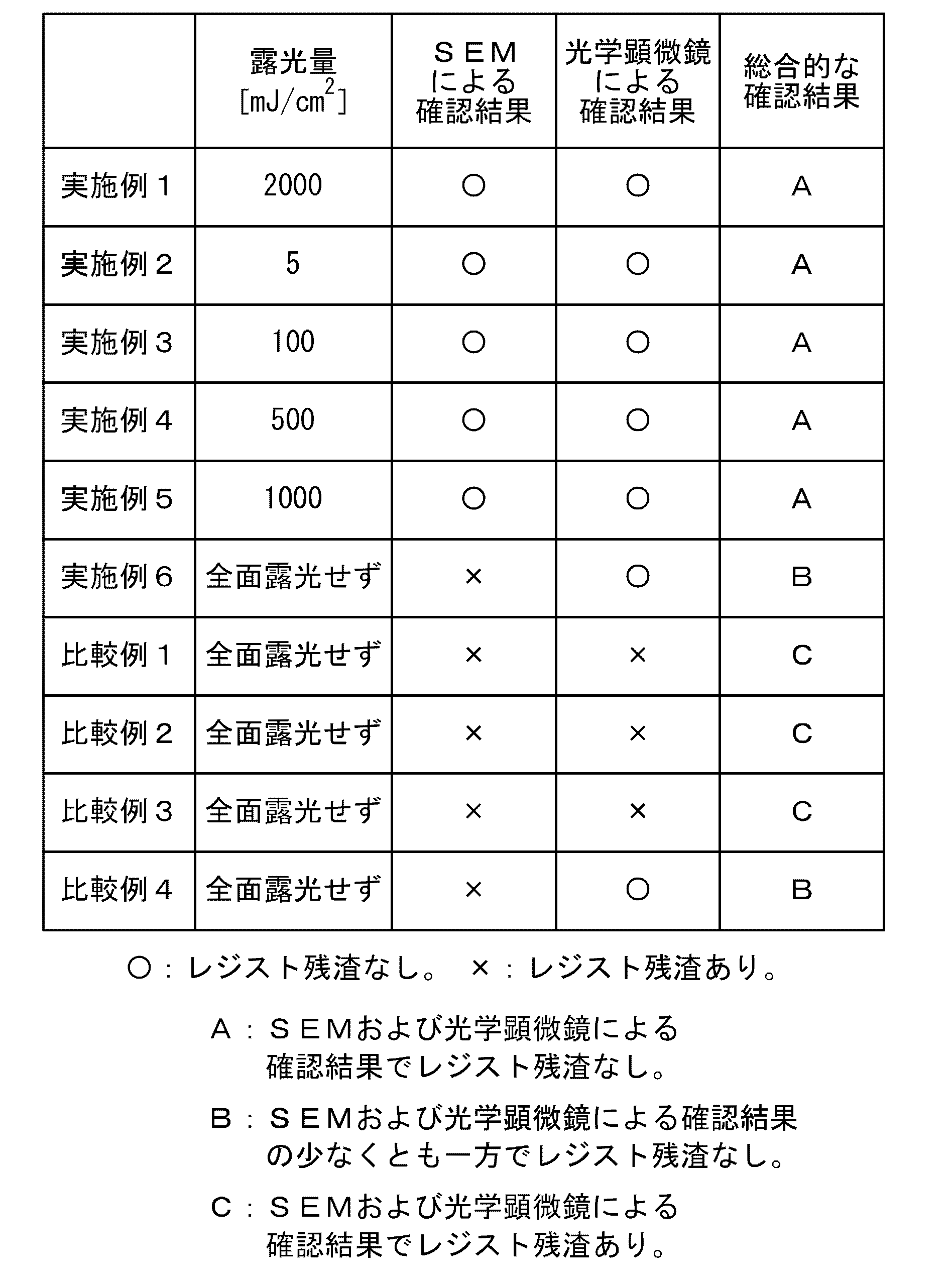
上記のように、実施例1~6の配線回路基板のうち不要なレジスト層5を5mJ/cm2以上の露光量で全面露光し、現像することにより得られた実施例1~5の配線回路基板には、レジスト残渣の発生が認められなかった。これに対して、実施例1~6の配線回路基板のうち不要なレジスト層5を全面露光および現像することなく剥離液により除去した実施例6の配線回路基板には、SEMによりレジスト残渣の発生が認められた。また、ドライフィルムレジストを引き剥がすことにより不要なレジスト層5を除去した比較例1~4の配線回路基板には、少なくともSEMによりレジスト残渣の発生が認められた。したがって、レジスト残渣の発生を抑制するためには、不要なレジスト層5を5mJ/cm2以上の露光量で全面露光し、現像することが好ましいことが分かった。
Claims (8)
- 長尺状の金属支持基板上に絶縁層が形成された積層体を用意する工程と、
ロールツーロールにより前記絶縁層上に感光性材料を含むめっきレジスト層を形成する工程と、
ロールツーロールにより前記めっきレジスト層を所定パターンで露光する工程と、
ロールツーロールにより前記所定パターンで露光されためっきレジスト層を現像することにより、前記めっきレジスト層に前記所定パターンまたは前記所定パターンとは逆パターンの開口を形成する工程と、
ロールツーロールにより前記開口内に導体層を形成する工程とを含み、
前記めっきレジスト層を形成する工程は、前記絶縁層上に感光性のめっきレジスト液を塗布し、塗布されためっきレジスト液に熱処理を施すことを含む、配線回路基板の製造方法。 - 前記めっきレジスト層を前記所定パターンで露光する工程は、前記所定パターンに対応するマスクと前記めっきレジスト層とを互いに接触させつつ、前記マスクを通して前記めっきレジスト層に露光光を照射する接触露光を行うことを含む、請求項1記載の配線回路基板の製造方法。
- 前記接触露光は、前記マスクと前記めっきレジスト層とが互いに接触した状態で、前記マスクと前記めっきレジスト層との間に予め定められた圧力以上の圧力を作用させることを含む、請求項2記載の配線回路基板の製造方法。
- 前記金属支持基板は、ステンレス鋼からなる、請求項1~3のいずれか一項に記載の配線回路基板の製造方法。
- 前記めっきレジスト液は、ポジ型の感光性樹脂からなり、
前記配線回路基板の製造方法は、
前記導体層を形成する工程の後、ロールツーロールにより前記めっきレジスト層の全体を露光する工程と、
ロールツーロールにより前記全体が露光されためっきレジスト層を現像することにより、前記絶縁層上のめっきレジスト層を除去する工程とをさらに含む、請求項1~4のいずれか一項に記載の配線回路基板の製造方法。 - 前記導体層を形成する工程の後、前記めっきレジスト層の全体を露光する工程において、前記めっきレジスト層の露光量は5mJ/cm2以上である、請求項5記載の配線回路基板の製造方法。
- 前記絶縁層は、感光性ポリイミドからなる、請求項1~6のいずれか一項に記載の配線回路基板の製造方法。
- 前記積層体を用意する工程の後、前記めっきレジスト層を形成する工程の前に、ロールツーロールにより前記絶縁層上にシード層を形成する工程をさらに含み、
めっきレジスト層を形成する工程において、前記めっきレジスト層は、前記シード層を介して前記絶縁層上に形成され、
前記導体層を形成する工程は、前記開口部内で露出するシード層上に電解めっきにより前記導体層を形成することを含む、請求項1~7のいずれか一項に記載の配線回路基板の製造方法。
Priority Applications (1)
| Application Number | Priority Date | Filing Date | Title |
|---|---|---|---|
| JP2023517578A JPWO2022230910A1 (ja) | 2021-04-30 | 2022-04-26 |
Applications Claiming Priority (2)
| Application Number | Priority Date | Filing Date | Title |
|---|---|---|---|
| JP2021-078091 | 2021-04-30 | ||
| JP2021078091 | 2021-04-30 |
Publications (1)
| Publication Number | Publication Date |
|---|---|
| WO2022230910A1 true WO2022230910A1 (ja) | 2022-11-03 |
Family
ID=83848477
Family Applications (1)
| Application Number | Title | Priority Date | Filing Date |
|---|---|---|---|
| PCT/JP2022/018986 Ceased WO2022230910A1 (ja) | 2021-04-30 | 2022-04-26 | 配線回路基板の製造方法 |
Country Status (3)
| Country | Link |
|---|---|
| JP (1) | JPWO2022230910A1 (ja) |
| TW (1) | TW202249552A (ja) |
| WO (1) | WO2022230910A1 (ja) |
Citations (6)
| Publication number | Priority date | Publication date | Assignee | Title |
|---|---|---|---|---|
| JPS52143769A (en) * | 1976-05-26 | 1977-11-30 | Hitachi Ltd | Removing method of positive type photo resist |
| JPH01253728A (ja) * | 1988-04-03 | 1989-10-11 | Nippon Synthetic Chem Ind Co Ltd:The | 感光性樹脂の製造方法および感光性樹脂組成物 |
| JPH07261388A (ja) * | 1994-03-25 | 1995-10-13 | Hitachi Chem Co Ltd | 感光性樹脂組成物、これを用いた感光性エレメント及びめっきレジストの製造法 |
| JPH10320736A (ja) * | 1997-05-22 | 1998-12-04 | Fujitsu Ltd | 配線パターンを有する磁気ヘッド用サスペンション素子の製造方法と製造設備 |
| JPH1117059A (ja) * | 1997-06-26 | 1999-01-22 | Toppan Printing Co Ltd | ボールグリッドアレイ基板及びその連続体 |
| JP2000290406A (ja) * | 1999-04-07 | 2000-10-17 | Toray Ind Inc | 耐熱性樹脂前駆体のパターン形成方法 |
-
2022
- 2022-04-26 WO PCT/JP2022/018986 patent/WO2022230910A1/ja not_active Ceased
- 2022-04-26 JP JP2023517578A patent/JPWO2022230910A1/ja active Pending
- 2022-04-28 TW TW111116209A patent/TW202249552A/zh unknown
Patent Citations (6)
| Publication number | Priority date | Publication date | Assignee | Title |
|---|---|---|---|---|
| JPS52143769A (en) * | 1976-05-26 | 1977-11-30 | Hitachi Ltd | Removing method of positive type photo resist |
| JPH01253728A (ja) * | 1988-04-03 | 1989-10-11 | Nippon Synthetic Chem Ind Co Ltd:The | 感光性樹脂の製造方法および感光性樹脂組成物 |
| JPH07261388A (ja) * | 1994-03-25 | 1995-10-13 | Hitachi Chem Co Ltd | 感光性樹脂組成物、これを用いた感光性エレメント及びめっきレジストの製造法 |
| JPH10320736A (ja) * | 1997-05-22 | 1998-12-04 | Fujitsu Ltd | 配線パターンを有する磁気ヘッド用サスペンション素子の製造方法と製造設備 |
| JPH1117059A (ja) * | 1997-06-26 | 1999-01-22 | Toppan Printing Co Ltd | ボールグリッドアレイ基板及びその連続体 |
| JP2000290406A (ja) * | 1999-04-07 | 2000-10-17 | Toray Ind Inc | 耐熱性樹脂前駆体のパターン形成方法 |
Also Published As
| Publication number | Publication date |
|---|---|
| TW202249552A (zh) | 2022-12-16 |
| JPWO2022230910A1 (ja) | 2022-11-03 |
Similar Documents
| Publication | Publication Date | Title |
|---|---|---|
| US6156484A (en) | Gray scale etching for thin flexible interposer | |
| KR100621550B1 (ko) | 테이프 배선 기판의 제조방법 | |
| TWI304523B (en) | Immersion lithography exposure apparatus and method | |
| CN101438636B (zh) | 抗蚀图的形成方法、电路基板的制造方法和电路基板 | |
| EP0403851A2 (en) | Excimer induced topography of flexible interconnect structures | |
| JP2009278070A (ja) | 配線回路基板の製造方法 | |
| CN101534608B (zh) | 一种柔性线路板的制作方法 | |
| WO2022230910A1 (ja) | 配線回路基板の製造方法 | |
| JP2019091840A (ja) | 配線層の製造方法並びにシード層の形成方法 | |
| JP2006114631A (ja) | 配線回路基板の製造方法 | |
| WO2021261525A1 (ja) | 配線構造体及びその製造方法、並びに半導体パッケージ | |
| JP2017038037A (ja) | 金属配線の製造方法 | |
| KR102830295B1 (ko) | Dfr 패턴의 재사용이 가능한 메탈 마스크 제조 방법 및 이에 의해 제조된 메탈 마스크 | |
| JP2025015323A (ja) | フレキシブル配線回路基板の製造方法 | |
| JPH1140619A (ja) | フープ状フレキシブル基板製造における基板変形防止装置 | |
| CN110621116A (zh) | 一种封装基板的制作方法 | |
| JP2886697B2 (ja) | 可撓性回路基板の製造法 | |
| TWI893768B (zh) | 雙面線路基板的側面配線製造方法 | |
| JPH11288080A (ja) | フォトレジスト印刷用マスクと印刷装置および印刷方法と電極箔の製造方法および印刷用ロール | |
| CN101945533B (zh) | 电路基板 | |
| JP5520140B2 (ja) | ドライフィルムレジストの薄膜化処理方法 | |
| JP7246615B2 (ja) | プリント配線板の製造方法及び積層体 | |
| JP2020049754A (ja) | 基板の製造方法 | |
| CN120835468A (zh) | 双面线路基板的侧面配线制造方法 | |
| JP4582277B2 (ja) | 柱状金属体の形成方法及び多層配線基板の製造方法 |
Legal Events
| Date | Code | Title | Description |
|---|---|---|---|
| 121 | Ep: the epo has been informed by wipo that ep was designated in this application |
Ref document number: 22795823 Country of ref document: EP Kind code of ref document: A1 |
|
| WWE | Wipo information: entry into national phase |
Ref document number: 2023517578 Country of ref document: JP |
|
| NENP | Non-entry into the national phase |
Ref country code: DE |
|
| 122 | Ep: pct application non-entry in european phase |
Ref document number: 22795823 Country of ref document: EP Kind code of ref document: A1 |