WO2022224985A1 - センサモジュール及び車両 - Google Patents
センサモジュール及び車両 Download PDFInfo
- Publication number
- WO2022224985A1 WO2022224985A1 PCT/JP2022/018263 JP2022018263W WO2022224985A1 WO 2022224985 A1 WO2022224985 A1 WO 2022224985A1 JP 2022018263 W JP2022018263 W JP 2022018263W WO 2022224985 A1 WO2022224985 A1 WO 2022224985A1
- Authority
- WO
- WIPO (PCT)
- Prior art keywords
- sensor
- temperature
- content
- processing unit
- sensor module
- Prior art date
- Legal status (The legal status is an assumption and is not a legal conclusion. Google has not performed a legal analysis and makes no representation as to the accuracy of the status listed.)
- Ceased
Links
Images




Classifications
-
- G—PHYSICS
- G01—MEASURING; TESTING
- G01D—MEASURING NOT SPECIALLY ADAPTED FOR A SPECIFIC VARIABLE; ARRANGEMENTS FOR MEASURING TWO OR MORE VARIABLES NOT COVERED IN A SINGLE OTHER SUBCLASS; TARIFF METERING APPARATUS; MEASURING OR TESTING NOT OTHERWISE PROVIDED FOR
- G01D3/00—Indicating or recording apparatus with provision for the special purposes referred to in the subgroups
- G01D3/028—Indicating or recording apparatus with provision for the special purposes referred to in the subgroups mitigating undesired influences, e.g. temperature, pressure
- G01D3/036—Indicating or recording apparatus with provision for the special purposes referred to in the subgroups mitigating undesired influences, e.g. temperature, pressure on measuring arrangements themselves
- G01D3/0365—Indicating or recording apparatus with provision for the special purposes referred to in the subgroups mitigating undesired influences, e.g. temperature, pressure on measuring arrangements themselves the undesired influence being measured using a separate sensor, which produces an influence related signal
Definitions
- the invention disclosed in this specification relates to a sensor module and a vehicle.
- the semiconductor device includes a driving section that drives the sensor and a processing section that processes the output of the sensor.
- the sensor and the processing unit are often manufactured in separate processes and sealed in one package. Since the sensor and the processing unit manufactured by different processes have different temperature dependencies, it is difficult to correct the temperature of the sensor module as a whole.
- a sensor module disclosed herein includes a sensor, a semiconductor device including a driving unit configured to drive the sensor and a processing unit configured to process an output signal of the sensor; a switching unit configured to switch whether to cut off or disable the supply of the output signal of the sensor to the processing unit; and a storage unit configured to store temperature correction content in a non-volatile manner. and a control unit configured to perform temperature correction on the driving unit and the processing unit based on the contents of the temperature correction.
- the vehicle disclosed in this specification includes the above sensor module.
- FIG. 1 is a diagram showing a schematic configuration of a sensor module according to one embodiment.
- FIG. 2 is a diagram showing a first configuration example of a sensor module according to one embodiment.
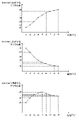
- FIG. 3 is a graph showing an example of contents of temperature correction for the output offset of the processing section alone, contents of temperature correction for the output offset of the driving section, and contents of temperature correction for the output offset of the sensor.
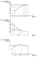
- FIG. 4 is a graph showing another example of the content of temperature correction regarding the output offset of the processing unit alone, the content of temperature correction regarding the output offset of the driving unit, and the content of temperature correction regarding the output offset of the sensor.
- FIG. 5 is a diagram showing a second configuration example of the sensor module according to one embodiment.
- FIG. 6 is a diagram showing a third configuration example of the sensor module according to one embodiment.
- FIG. 7 is a diagram showing a fourth configuration example of the sensor module according to one embodiment.
- FIG. 8 is an external view of a vehicle according to one embodiment.
- FIG. 1 is a diagram showing a schematic configuration of a sensor module according to one embodiment.
- the sensor module 100 shown in FIG. 1 includes a semiconductor device 1, a sensor 2, and terminals T101 to T103.
- the semiconductor device 1 is, for example, an LSI (Large Scale Integration).
- the semiconductor device 1 includes a digital circuit 11, a driving section 12, a resistor 13, a processing section 14, and terminals T11 to T17.
- the sensor module 100 includes the drive section 12 and the processing section 14 .
- the sensor 2 collects information to be detected, converts the collected information into an electrical signal, and outputs the electrical signal.
- the sensor 2 has terminals T21 to T24.
- the detection target of the sensor 2 is not particularly limited as long as it is other than temperature.
- the format of the output signal of the sensor 2 is not particularly limited, the sensor 2 outputs a differential voltage signal in this embodiment.
- the semiconductor device 1 and the sensor 2 are manufactured by separate processes. For example, the semiconductor device 1 is manufactured by a silicon semiconductor process, and the sensor 2 is manufactured by a compound semiconductor process.
- the terminal T101 is configured to receive the power supply voltage VDD, and is physically and electrically connected to the terminal T11 inside the sensor module 100 .
- the terminal T102 is a terminal configured to be connected to a ground potential, and is physically and electrically connected to the terminal T12 inside the sensor module 100.
- the terminal T103 is configured to output the output signal of the processing unit 14 (to be described later) to the outside of the sensor module 100, and is physically and electrically connected to the terminal T17 inside the sensor module 100.
- the terminals T13 to T16 are physically and electrically connected to the terminals T21 to T24 inside the sensor module 100, respectively.
- the digital circuit 11 is a circuit that processes digital signals and controls the operation of the sensor module 100 as a whole.
- the digital circuit 11 includes a storage section 11A and a control section 11B. That is, the sensor module 100 includes a storage section 11A and a control section 11B.
- the storage unit 11A is configured to store the content of temperature correction in a non-volatile manner.
- the control unit 11B is configured to perform temperature correction of the driving unit 12 and the processing unit 14 based on the content of temperature correction stored in the storage unit 11A.
- the drive unit 12 is configured to drive the sensor 2 .
- a drive current output from the drive unit 12 is supplied to the terminal T21 of the sensor 2 via the terminal T13.
- a first end of the resistor 13 is physically and electrically connected to the terminal T14 inside the semiconductor device 1, and a second end of the resistor 13 is physically and electrically connected to the terminal T12 inside the semiconductor device 1. .
- the resistor 13 converts the driving current of the sensor 2 into voltage, and the voltage corresponding to the driving current of the sensor 2 is fed back to the driving section 12 .
- the drive unit 12 feedback-controls the drive current of the sensor 2 .
- the processing unit 14 is configured to process the output signal of the sensor 2 .
- the processing unit 14 includes a first processing unit 14A and a second processing unit 14B.
- the first processing unit 14A is configured to receive and process the output signal of the sensor 2. Specifically, the output signals of the sensor 2 output from the terminals T23 and T24 of the sensor 2 are supplied to the first processing section 14A via the terminals T15 and T16.
- the first processing section 14A is a single amplifier, the first processing section 14A is not limited to a single amplifier, and may have a configuration in which a plurality of amplifiers are connected in series, for example.
- the second processing unit 14B is configured to receive and process the output signal of the first processing unit 14A.
- the output signal of the second processing section 14B is supplied to the terminal T103 via the terminal T17.
- the second processing section 14B is a single amplifier, but the second processing section 14B is not limited to a single amplifier, and may have a configuration in which a plurality of amplifiers are connected in series, for example. .
- a switching unit SW1 is provided inside the first processing unit 14A. That is, the sensor module 100 has a switching section SW1.
- the switching unit SW1 is configured to switch whether to disable the supply of the output signal of the sensor 2 to the processing unit 14 or not. Specifically, the switching unit SW1 is configured to switch whether to short-circuit the terminal T23 and the terminal T24.
- the switching unit SW1 may be configured to switch whether to cut off the supply of the output signal of the sensor 2 to the processing unit 14 or not.
- the switching unit SW1 is provided between the terminals T15 and T16 and the processing unit 14 instead of inside the first processing unit 14A, and the switching unit SW1 turns on/off electrical connection between the terminals T15 and T16 and the processing unit 14. You may
- the switching unit SW1 disables the supply of the output signal of the sensor 2 to the processing unit 14 .
- This makes it possible to distinguish between the temperature characteristics of the semiconductor device 1 and the temperature characteristics of the sensor 2 .
- the output signal of the terminal T103 is taken into the evaluation device, which is an external device of the sensor module 100, while changing the ambient temperature of the sensor module 100.
- the evaluation device which is an external device of the sensor module 100
- the terminal T103 of the sensor module 100 and the input terminal of the evaluation device are connected by a cable or the like.
- the evaluation device Based on the output signal from the terminal T103, the evaluation device prepares the content of the temperature correction regarding the output offset of the processing unit 14 alone.
- the content of the temperature correction regarding the output offset of the processing unit 14 alone is stored in the storage unit 11A.
- the control unit 11B performs temperature correction on the second processing unit 14B based on the content of temperature correction regarding the output offset of the processing unit 14 alone, and transfers the output signal of the sensor 2 to the processing unit 14.
- the output signal at the terminal T103 is taken into the evaluation device while the supply is not disabled.
- the sensor 2 does not have to sense the object to be sensed (including the case where the sensor 2 performs weak sensing that can be regarded as not sensing), and the output signal of the sensor 2 offsets the output offset of the sensor 2. Sensing objects that are negligibly large may be sensed.
- the evaluation device creates contents of temperature correction relating to the output offset of the driving section 12 based on the output signal of the terminal T103.
- the content of temperature correction regarding the output offset of the processing unit 14 alone and the content of temperature correction regarding the output offset of the drive unit 12 are stored in the storage unit 11A.
- the control unit 11B temperature-compensates the driving unit 12 and the second processing unit 14B based on the content of the temperature correction regarding the output offset of the processing unit 14 alone and the content of the temperature correction regarding the output offset of the driving unit 12, and the sensor 2 A state in which the object to be sensed is not being sensed (including a case in which weak sensing is being performed that can be regarded as not being sensed) and the supply of the output signal of the sensor 2 to the processing unit 14 is not disabled.
- the output signal of the terminal T103 is taken into the evaluation device.
- the above-described evaluation device prepares contents of temperature correction regarding the output offset of the sensor 2 based on the output signal of the terminal T103.
- the content of the temperature correction related to the output offset of the sensor 2 is stored in the storage unit 11A.
- the control unit 11B controls the driving unit 12, the driving unit 12, and the sensor 2 based on the content of the temperature correction regarding the output offset of the processing unit 14 alone, the content of the temperature correction regarding the output offset of the driving unit 12, and the content of the temperature correction regarding the output offset of the sensor 2.
- the temperature of the second processing section 14B and the first processing section 14A can be corrected.
- the sensor module 100 includes the switching unit SW1, it is possible to separate the temperature characteristics of the semiconductor device 1 and the temperature characteristics of the sensor 2 from each other. Therefore, it becomes easy for the evaluation device, which is an external device of the sensor module 100 , to acquire the content of the temperature correction of the sensor module 100 . As a result, the sensor module 100 can easily perform temperature correction.
- the sensor module 100 may be configured to have the function of the evaluation device.
- the contents of temperature correction stored in the storage unit 11A include the contents of temperature correction regarding the output offset of the processing unit 14 alone, the contents of temperature correction regarding the output offset of the driving unit 12, and the contents of temperature correction regarding the output offset of the sensor 2. Since the content is included, temperature correction of each of the processing unit 14 alone, the drive unit 12, and the sensor 2 can be performed appropriately.
- the content of temperature correction related to the output offset of the processing unit 14 alone, the content of temperature correction related to the output offset of the drive unit 12, the content of temperature correction related to the output offset of the sensor 2, and the drive unit to be controlled by the temperature correction 12, the second processing unit 14B, and the first processing unit 14A are in one-to-one correspondence, so temperature correction control is easy.
- FIG. 2 is a diagram showing a first configuration example of the sensor module 100.
- the sensor module 100A shown in FIG. 2 has a terminal T104.
- the semiconductor device 1 of the sensor module 100A also includes DACs (Digital to Analog Converters) 15A to 15C, an ADC (Analog to Digital Converter) 16, a temperature sensor 17, and a terminal T18. That is, the sensor module 100A includes DACs 15A-15C. Further, in the sensor module 100A, the digital circuit 11 has a communication section 11C.
- DACs Digital to Analog Converters
- ADC Analog to Digital Converter
- the control unit 11B controls the second processing unit 14B via the DAC 15C to perform temperature correction regarding the output offset of the processing unit 14 alone.
- the control unit 11B controls the driving unit 12 via the DAC 15A to perform temperature correction regarding the output offset of the driving unit 12.
- the control unit 11B controls the first processing unit 14A via the DAC 15B to perform temperature correction regarding the output offset of the sensor 2.
- the control section 11B can control the second processing section 14B, the driving section 12, and the first processing section 14A with a simple configuration.
- the communication unit 11C can acquire the signal and information supplied to the terminal T104 via the terminal T18. For example, by connecting the output terminal of the evaluation device and the terminal T104 with a cable or the like, the communication unit 11C can transmit the content of the temperature correction regarding the output offset of the processing unit 14 alone from the evaluation device and the output offset of the driving unit 12. The content of the temperature correction and the content of the temperature correction related to the output offset of the sensor 2 can be obtained.
- FIG. 3 is a graph showing an example of the content of temperature correction regarding the output offset of the processing unit 14 alone, the content of temperature correction regarding the output offset of the driving unit 12, and the content of temperature correction regarding the output offset of the sensor 2.
- FIG. The horizontal axis of each graph shown in FIG. 3 represents time, the vertical axis of the upper graph shown in FIG. The axis represents the digital value that the control section 11B supplies to the DAC 15A, and the vertical axis of the lower graph shown in FIG. 3 represents the digital value that the control section 11B supplies to the DAC 15B.
- a data table corresponding to nine black circles in the upper graph shown in FIG. 3 is stored in the storage section 11A as contents of temperature correction relating to the output offset of the processing section 14 alone. Digital values between two bullets are linearly interpolated, for example.
- a data table corresponding to nine black circles in the central graph shown in FIG. Digital values between two bullets are linearly interpolated, for example.
- a data table corresponding to nine black circles in the lower graph shown in FIG. Digital values between two bullets are linearly interpolated, for example.
- the values of the first temperature data t1 are the same, and the values of the second temperature data t2 to the ninth temperature data t9 are also the same.
- each temperature data can be set to a different value depending on the content of temperature correction regarding the output offset of the processing unit 14 alone, the content of temperature correction regarding the output offset of the drive unit 12, and the content of temperature correction regarding the output offset of the sensor 2. is preferably As a result, for example, temperature data can be concentrated near the inflection point of the graph, and the accuracy of temperature correction near the inflection point of the graph can be improved.
- each graph shown in FIG. 4 represents time
- the vertical axis of the upper graph shown in FIG. The axis represents the digital value that the control section 11B supplies to the DAC 15A
- the vertical axis of the lower graph shown in FIG. 4 represents the digital value that the control section 11B supplies to the DAC 15B.
- the eighth temperature data t8 is set to different values.
- the storage unit 11A may store a function indicating the relationship between temperature and digital value instead of the data table.
- the semiconductor device 1 of the sensor module 100A includes the temperature sensor 17. That is, the sensor module 100A has the temperature sensor 17 . An output signal (temperature information) of the temperature sensor 17 is converted into a digital signal by the ADC 16 and supplied to the digital circuit 11 . The digital circuit 11 temperature-compensates the drive unit 12 and the processing unit 14 based on the temperature information and the content of the temperature compensation stored in the storage unit 11A.
- the sensor module 100A includes the temperature sensor 17, there is no need to provide an input terminal for inputting temperature information to the sensor module 100A. As a result, it is possible to reduce the size and cost of the sensor module 100A.
- FIG. 5 is a diagram showing a second configuration example of the sensor module 100.
- FIG. A sensor module 100B shown in FIG. 5 differs from the sensor module 100A in that a temperature sensor is not provided inside the semiconductor device 1, and is basically the same as the sensor module 100A in other respects.
- the sensor module 100B includes a sensor 3.
- the semiconductor device 1 of the sensor module 100B has a terminal T19.
- An output signal (temperature information) from the sensor 3 is supplied to the ADC 16 via the terminal T19.
- FIG. 6 is a diagram showing a third configuration example of the sensor module 100.
- FIG. A sensor module 100C shown in FIG. 6 differs from the sensor module 100A in that the semiconductor device 1 includes a constant voltage source 18 and a selector 19, and otherwise is basically the same as the sensor module 100A.
- the constant voltage source 18 is configured to output a constant voltage.
- the constant voltage means a voltage that is constant in an ideal state, and is actually a voltage that can slightly fluctuate due to temperature changes or the like.
- a specific circuit configuration of the constant voltage source 18 is not particularly limited, but in this configuration example, the constant voltage source 18 is a bandgap type constant voltage circuit.
- the output signal (temperature information) of the sensor 3 is supplied to the first input terminal of the selector 19 .
- a constant voltage output from the constant voltage source 18 is supplied to the second input terminal of the selector 19 .
- the selector 19 is configured to select either the output signal of the sensor 3 or the constant voltage.
- the ADC 16 converts the output of the selector 19 into a digital signal and supplies it to the digital circuit 11 .
- the control unit 11B is configured to correct the output signal (temperature information) of the sensor 3 based on the output of the ADC 16 when the selector 19 selects the constant voltage.
- the selector 19 periodically selects the constant voltage only for a short period of time and selects the output signal of the sensor 3 at other times.
- the sensor module 101C improves the accuracy of the temperature information by correcting the temperature information, so the accuracy of the temperature correction of the driving unit and the processing unit is also improved.
- FIG. 7 is a diagram showing a fourth configuration example of the sensor module 100.
- FIG. A sensor module 100D shown in FIG. 7 differs from the sensor module 100C in that a temperature sensor is not provided inside the semiconductor device 1, and is basically the same as the sensor module 100C in other respects.
- the sensor module 100D includes a sensor 3.
- the semiconductor device 1 of the sensor module 100D has a terminal T19.
- the output signal (temperature information) of the sensor 3 is supplied to the first input terminal of the selector 19 via the terminal T19.
- the device or equipment on which the sensor module 100 described above is mounted is not limited, it is particularly useful to mount the sensor module 100 on a device or equipment in which the temperature in the usage environment changes greatly.
- the sensor module 100 is mounted on a vehicle X shown in FIG. 8, for example. That is, the vehicle X has the sensor module 100 .
- the sensor 2 provided in the sensor module 100 is a magnetic sensor, and the rotor rotational position of a predetermined motor provided in the vehicle X is detected based on the detection signal of the magnetic sensor. Just do it.
- the sensor modules 100A to 100D described above are configured to incorporate a temperature sensor, but the temperature information detected by the temperature sensor provided outside the sensor module is acquired by the control unit provided inside the sensor module.
- the sensor modules (100A to 100D) described above include a sensor (2), a driving section (12) configured to drive the sensor, and a processing section (12) configured to process the output signal of the sensor. 14), a switching unit (SW1) configured to switch whether to cut off or disable the supply of the output signal of the sensor to the processing unit, and contents of temperature correction. and a control unit (11B) configured to perform temperature correction of the driving unit and the processing unit based on the content of the temperature correction. It is a configuration (first configuration) provided.
- the sensor module which is the first configuration, has a configuration that enables separation of the temperature characteristics of the semiconductor device and the temperature characteristics of the sensor. Therefore, the sensor module can easily perform temperature correction.
- the content of the temperature correction includes a first content related to the output offset of the processing unit alone, a second content related to the output offset of the drive unit, and a second content related to the output offset of the sensor. 3 content and the configuration (second configuration).
- the sensor module having the second configuration above can appropriately perform temperature correction for each of the processing unit, drive unit, and sensor.
- the processing units include a first processing unit (14A) configured to receive and process an output signal of the sensor, and receive the output signal of the first processing unit. and a second processing unit (14B) configured to process the second processing unit (14B), wherein the control unit temperature-compensates the second processing unit based on the first content, and the driving unit based on the second content may be temperature-corrected, and the temperature of the first processing unit may be corrected based on the third content (third configuration).
- first to third DACs (15A to 15C) are provided, and the control section corrects the temperature of the second processing section via the first DAC, and corrects the temperature of the second processing section via the second DAC.
- a configuration (fourth configuration) may be configured such that the driving section is temperature-corrected via the third DAC, and the first processing section is temperature-corrected via the third DAC.
- the control section can control the second processing section, the driving section, and the first processing section with a simple configuration.
- each of the first content, the second content, and the third content is a data table, and the temperature data of the data table is the first content,
- the second content and the third content may be set to different values (fifth configuration).
- the sensor module having the fifth configuration concentrates the temperature data near the inflection point of the graph obtained by interpolating the data table to improve the accuracy of temperature correction near the inflection point of the graph. be able to.
- the temperature sensor (3, 17) is provided, and the control unit acquires temperature information detected by the temperature sensor, and the temperature information and the temperature A configuration (sixth configuration) configured to correct the temperatures of the driving unit and the processing unit based on the content of the correction may be employed.
- the sensor module of the sixth configuration has a built-in temperature sensor, it does not require an input terminal for inputting temperature information. As a result, it is possible to reduce the size and cost of the sensor module.
- a constant voltage source (18) configured to output a constant voltage, and configured to select either the output of the temperature sensor or the constant voltage.
- a selector (19); and an ADC (16) configured to analog-to-digital convert an output of the selector, wherein the controller controls the ADC when the selector selects the constant voltage.
- a configuration (seventh configuration) may be configured to correct the temperature information based on the output of.
- the sensor module having the seventh configuration improves the accuracy of the temperature information by correcting the temperature information, so that the temperature correction accuracy of the driving unit and the processing unit is also improved.
- the vehicle (X) described above has a configuration (eighth configuration) including the sensor module having any one of the first to seventh configurations.
- the mounted sensor module can easily perform temperature correction.
Landscapes
- Physics & Mathematics (AREA)
- General Physics & Mathematics (AREA)
- Measuring Temperature Or Quantity Of Heat (AREA)
- Indication And Recording Devices For Special Purposes And Tariff Metering Devices (AREA)
Abstract
Description
11 デジタル回路
11A 記憶部
11B 制御部
11C 通信部
12 駆動部
13 抵抗
14 処理部
14A 第1処理部
14B 第2処理部
15A~15C DAC
16 ADC
17 温度センサ
18 定電圧源
19 セレクタ
2 センサ
3 温度センサ
100、100A~100D センサモジュール
SW1 切替部
T11~T19、T21~T24、T101~T104 端子
X 車両
Claims (8)
- センサと、
前記センサを駆動するように構成される駆動部及び前記センサの出力信号を処理するように構成される処理部を含む半導体装置と、
前記センサの出力信号の前記処理部への供給を遮断又は無効にするか否かを切り替えるように構成される切替部と、
温度補正の内容を不揮発的に記憶するように構成される記憶部と、
前記温度補正の内容に基づき、前記駆動部及び前記処理部を温度補正するように構成される制御部と、
を備える、センサモジュール。 - 前記温度補正の内容は、
前記処理部単体の出力オフセットに関する第1内容と、
前記駆動部の出力オフセットに関する第2内容と、
前記センサの出力オフセットに関する第3内容と、
を含む、請求項1に記載のセンサモジュール。 - 前記処理部は、前記センサの出力信号を受け取って処理するように構成される第1処理部と、前記第1処理部の出力信号を受け取って処理するように構成される第2処理部と、を備え、
前記制御部は、前記第1内容に基づき前記第2処理部を温度補正し、前記第2内容に基づき前記駆動部を温度補正し、前記第3内容に基づき前記第1処理部を温度補正するように構成される、請求項2に記載のセンサモジュール。 - 第1~第3DACを備え、
前記制御部は、前記第1DACを介して前記第2処理部を温度補正し、前記第2DACを介して前記駆動部を温度補正し、前記第3DACを介して前記第1処理部を温度補正するように構成される、請求項3に記載のセンサモジュール。 - 前記第1内容、前記第2内容、及び前記第3内容はそれぞれデータテーブルであり、
前記データテーブルの温度データは前記第1内容、前記第2内容、及び前記第3内容それぞれで異なる値に設定可能である、請求項2~4のいずれか一項に記載のセンサモジュール。 - 温度センサを備え、
前記制御部は、前記温度センサによって検知された温度情報を取得し、前記温度情報及び前記温度補正の内容に基づき、前記駆動部及び前記処理部を温度補正するように構成される、請求項1~5のいずれか一項に記載のセンサモジュール。 - 定電圧を出力するように構成される定電圧源と、
前記温度センサの出力と前記定電圧のいずれか一方を選択するように構成されるセレクタと、
前記セレクタの出力をアナログ・デジタル変換するように構成されるADCと、
を備え、
前記制御部は、前記セレクタが前記定電圧を選択しているときの前記ADCの出力に基づき、前記温度情報を補正するように構成される、請求項6に記載のセンサモジュール。 - 請求項1~7のいずれか一項に記載のセンサモジュールを備える、車両。
Priority Applications (3)
| Application Number | Priority Date | Filing Date | Title |
|---|---|---|---|
| JP2023515495A JP7824279B2 (ja) | 2021-04-21 | 2022-04-20 | センサモジュール及び車両 |
| CN202280029460.XA CN117203500A (zh) | 2021-04-21 | 2022-04-20 | 传感器模块和车辆 |
| US18/484,754 US20240035852A1 (en) | 2021-04-21 | 2023-10-11 | Sensor module and vehicle |
Applications Claiming Priority (2)
| Application Number | Priority Date | Filing Date | Title |
|---|---|---|---|
| JP2021071585 | 2021-04-21 | ||
| JP2021-071585 | 2021-04-21 |
Related Child Applications (1)
| Application Number | Title | Priority Date | Filing Date |
|---|---|---|---|
| US18/484,754 Continuation US20240035852A1 (en) | 2021-04-21 | 2023-10-11 | Sensor module and vehicle |
Publications (1)
| Publication Number | Publication Date |
|---|---|
| WO2022224985A1 true WO2022224985A1 (ja) | 2022-10-27 |
Family
ID=83722341
Family Applications (1)
| Application Number | Title | Priority Date | Filing Date |
|---|---|---|---|
| PCT/JP2022/018263 Ceased WO2022224985A1 (ja) | 2021-04-21 | 2022-04-20 | センサモジュール及び車両 |
Country Status (4)
| Country | Link |
|---|---|
| US (1) | US20240035852A1 (ja) |
| JP (1) | JP7824279B2 (ja) |
| CN (1) | CN117203500A (ja) |
| WO (1) | WO2022224985A1 (ja) |
Citations (3)
| Publication number | Priority date | Publication date | Assignee | Title |
|---|---|---|---|---|
| JP2004108825A (ja) * | 2002-09-13 | 2004-04-08 | Mitsubishi Electric Corp | 温度検出装置および温度検出手段を備えた電力変換装置 |
| JP2010156686A (ja) * | 2008-12-08 | 2010-07-15 | Robert Bosch Gmbh | オフセットが低減されている集積センサアレイ |
| JP2015204608A (ja) * | 2014-04-16 | 2015-11-16 | 富士電機株式会社 | 物理量センサ装置および物理量センサ装置の調整方法 |
Family Cites Families (5)
| Publication number | Priority date | Publication date | Assignee | Title |
|---|---|---|---|---|
| JP5757772B2 (ja) * | 2011-04-13 | 2015-07-29 | ルネサスエレクトロニクス株式会社 | 半導体装置、及びデータ生成方法 |
| US9991792B2 (en) * | 2014-08-27 | 2018-06-05 | Intersil Americas LLC | Current sensing with RDSON correction |
| EP3351905B1 (en) * | 2017-01-19 | 2020-03-11 | Melexis Technologies NV | Sensor with self diagnostic function |
| JP7333705B2 (ja) | 2019-04-03 | 2023-08-25 | ホーチキ株式会社 | 回路システム |
| DE102019207657B4 (de) * | 2019-05-24 | 2022-01-27 | Vitesco Technologies GmbH | Sensormodul, Verfahren zum Bereitstellen eines analogen Sensormodulsignals und Sensorsystem |
-
2022
- 2022-04-20 WO PCT/JP2022/018263 patent/WO2022224985A1/ja not_active Ceased
- 2022-04-20 CN CN202280029460.XA patent/CN117203500A/zh active Pending
- 2022-04-20 JP JP2023515495A patent/JP7824279B2/ja active Active
-
2023
- 2023-10-11 US US18/484,754 patent/US20240035852A1/en active Pending
Patent Citations (3)
| Publication number | Priority date | Publication date | Assignee | Title |
|---|---|---|---|---|
| JP2004108825A (ja) * | 2002-09-13 | 2004-04-08 | Mitsubishi Electric Corp | 温度検出装置および温度検出手段を備えた電力変換装置 |
| JP2010156686A (ja) * | 2008-12-08 | 2010-07-15 | Robert Bosch Gmbh | オフセットが低減されている集積センサアレイ |
| JP2015204608A (ja) * | 2014-04-16 | 2015-11-16 | 富士電機株式会社 | 物理量センサ装置および物理量センサ装置の調整方法 |
Also Published As
| Publication number | Publication date |
|---|---|
| CN117203500A (zh) | 2023-12-08 |
| JP7824279B2 (ja) | 2026-03-04 |
| US20240035852A1 (en) | 2024-02-01 |
| JPWO2022224985A1 (ja) | 2022-10-27 |
Similar Documents
| Publication | Publication Date | Title |
|---|---|---|
| US9128163B2 (en) | Voltage measuring apparatus for plural battery | |
| KR20150096323A (ko) | 오프셋 보상을 갖는 증폭기 | |
| US9360344B2 (en) | Parallel reading of an analog sensor by two control units | |
| US8319677B2 (en) | Semiconductor integrated circuit device having A/D converter with impedance matching circuit | |
| US9148133B2 (en) | Trimming circuit, power supply including trimming circuit, and trimming method | |
| TW201603479A (zh) | 具有校正功能之驅動裝置及其應用之無線充電驅動系統 | |
| US9395213B2 (en) | Sensor signal processing device and readout integrated circuit including the same | |
| JP4206574B2 (ja) | 組電池の電圧検出回路 | |
| WO2022224985A1 (ja) | センサモジュール及び車両 | |
| US10816946B2 (en) | Signal processing device | |
| EP1788398A1 (en) | Detector | |
| CN104515611B (zh) | 一种感温电路及温度传感器 | |
| JP2011069809A (ja) | 制御システム及びそれに用いる半導体素子 | |
| EP4060898A1 (en) | Current output module | |
| US10003351B2 (en) | Semiconductor device including analog-to-digital conversion circuit | |
| US10063248B2 (en) | Driver arrangement and method for providing an analog output signal | |
| KR20150088603A (ko) | 출력 방식의 변환이 가능한 캘리브레이션 압력센서 모듈 | |
| CN115361018B (zh) | 一种adc校正电路 | |
| CN118783958A (zh) | 模数转换电路、芯片及电子设备 | |
| JP6314681B2 (ja) | 排気ガスセンサのa/d変換データ補正システム | |
| WO2018078823A1 (ja) | アナログデジタル変換装置及びアナログデジタル変換方法 | |
| WO2012081960A1 (en) | Dual- function successive approximation analog to digital converter (sa-adc) | |
| JP6972705B2 (ja) | 電子装置 | |
| US20090241664A1 (en) | Angular rate detection apparatus providing stable output | |
| JP2014086748A (ja) | 逐次比較型a/dコンバータ及び逐次比較型a/dコンバータの補正チャージ方法 |
Legal Events
| Date | Code | Title | Description |
|---|---|---|---|
| 121 | Ep: the epo has been informed by wipo that ep was designated in this application |
Ref document number: 22791756 Country of ref document: EP Kind code of ref document: A1 |
|
| WWE | Wipo information: entry into national phase |
Ref document number: 2023515495 Country of ref document: JP |
|
| WWE | Wipo information: entry into national phase |
Ref document number: 202280029460.X Country of ref document: CN |
|
| NENP | Non-entry into the national phase |
Ref country code: DE |
|
| 122 | Ep: pct application non-entry in european phase |
Ref document number: 22791756 Country of ref document: EP Kind code of ref document: A1 |