WO2022224847A1 - 出力回路 - Google Patents
出力回路 Download PDFInfo
- Publication number
- WO2022224847A1 WO2022224847A1 PCT/JP2022/017394 JP2022017394W WO2022224847A1 WO 2022224847 A1 WO2022224847 A1 WO 2022224847A1 JP 2022017394 W JP2022017394 W JP 2022017394W WO 2022224847 A1 WO2022224847 A1 WO 2022224847A1
- Authority
- WO
- WIPO (PCT)
- Prior art keywords
- wiring
- power supply
- output
- extending
- semiconductor chip
- Prior art date
- Legal status (The legal status is an assumption and is not a legal conclusion. Google has not performed a legal analysis and makes no representation as to the accuracy of the status listed.)
- Ceased
Links
Images


Classifications
-
- H—ELECTRICITY
- H10—SEMICONDUCTOR DEVICES; ELECTRIC SOLID-STATE DEVICES NOT OTHERWISE PROVIDED FOR
- H10D—INORGANIC ELECTRIC SEMICONDUCTOR DEVICES
- H10D89/00—Aspects of integrated devices not covered by groups H10D84/00 - H10D88/00
- H10D89/10—Integrated device layouts
-
- H—ELECTRICITY
- H10—SEMICONDUCTOR DEVICES; ELECTRIC SOLID-STATE DEVICES NOT OTHERWISE PROVIDED FOR
- H10D—INORGANIC ELECTRIC SEMICONDUCTOR DEVICES
- H10D84/00—Integrated devices formed in or on semiconductor substrates that comprise only semiconducting layers, e.g. on Si wafers or on GaAs-on-Si wafers
- H10D84/90—Masterslice integrated circuits
- H10D84/903—Masterslice integrated circuits comprising field effect technology
- H10D84/907—CMOS gate arrays
-
- H—ELECTRICITY
- H10—SEMICONDUCTOR DEVICES; ELECTRIC SOLID-STATE DEVICES NOT OTHERWISE PROVIDED FOR
- H10W—GENERIC PACKAGES, INTERCONNECTIONS, CONNECTORS OR OTHER CONSTRUCTIONAL DETAILS OF DEVICES COVERED BY CLASS H10
- H10W20/00—Interconnections in chips, wafers or substrates
- H10W20/40—Interconnections external to wafers or substrates, e.g. back-end-of-line [BEOL] metallisations or vias connecting to gate electrodes
- H10W20/41—Interconnections external to wafers or substrates, e.g. back-end-of-line [BEOL] metallisations or vias connecting to gate electrodes characterised by their conductive parts
- H10W20/427—Power or ground buses
-
- H—ELECTRICITY
- H10—SEMICONDUCTOR DEVICES; ELECTRIC SOLID-STATE DEVICES NOT OTHERWISE PROVIDED FOR
- H10D—INORGANIC ELECTRIC SEMICONDUCTOR DEVICES
- H10D84/00—Integrated devices formed in or on semiconductor substrates that comprise only semiconducting layers, e.g. on Si wafers or on GaAs-on-Si wafers
- H10D84/01—Manufacture or treatment
- H10D84/0123—Integrating together multiple components covered by H10D12/00 or H10D30/00, e.g. integrating multiple IGBTs
- H10D84/0126—Integrating together multiple components covered by H10D12/00 or H10D30/00, e.g. integrating multiple IGBTs the components including insulated gates, e.g. IGFETs
- H10D84/0149—Manufacturing their interconnections or electrodes, e.g. source or drain electrodes
-
- H—ELECTRICITY
- H10—SEMICONDUCTOR DEVICES; ELECTRIC SOLID-STATE DEVICES NOT OTHERWISE PROVIDED FOR
- H10D—INORGANIC ELECTRIC SEMICONDUCTOR DEVICES
- H10D84/00—Integrated devices formed in or on semiconductor substrates that comprise only semiconducting layers, e.g. on Si wafers or on GaAs-on-Si wafers
- H10D84/01—Manufacture or treatment
- H10D84/0123—Integrating together multiple components covered by H10D12/00 or H10D30/00, e.g. integrating multiple IGBTs
- H10D84/0126—Integrating together multiple components covered by H10D12/00 or H10D30/00, e.g. integrating multiple IGBTs the components including insulated gates, e.g. IGFETs
- H10D84/0165—Integrating together multiple components covered by H10D12/00 or H10D30/00, e.g. integrating multiple IGBTs the components including insulated gates, e.g. IGFETs the components including complementary IGFETs, e.g. CMOS devices
- H10D84/0186—Manufacturing their interconnections or electrodes, e.g. source or drain electrodes
-
- H—ELECTRICITY
- H10—SEMICONDUCTOR DEVICES; ELECTRIC SOLID-STATE DEVICES NOT OTHERWISE PROVIDED FOR
- H10D—INORGANIC ELECTRIC SEMICONDUCTOR DEVICES
- H10D84/00—Integrated devices formed in or on semiconductor substrates that comprise only semiconducting layers, e.g. on Si wafers or on GaAs-on-Si wafers
- H10D84/01—Manufacture or treatment
- H10D84/02—Manufacture or treatment characterised by using material-based technologies
- H10D84/03—Manufacture or treatment characterised by using material-based technologies using Group IV technology, e.g. silicon technology or silicon-carbide [SiC] technology
- H10D84/038—Manufacture or treatment characterised by using material-based technologies using Group IV technology, e.g. silicon technology or silicon-carbide [SiC] technology using silicon technology, e.g. SiGe
-
- H—ELECTRICITY
- H10—SEMICONDUCTOR DEVICES; ELECTRIC SOLID-STATE DEVICES NOT OTHERWISE PROVIDED FOR
- H10D—INORGANIC ELECTRIC SEMICONDUCTOR DEVICES
- H10D84/00—Integrated devices formed in or on semiconductor substrates that comprise only semiconducting layers, e.g. on Si wafers or on GaAs-on-Si wafers
- H10D84/80—Integrated devices formed in or on semiconductor substrates that comprise only semiconducting layers, e.g. on Si wafers or on GaAs-on-Si wafers characterised by the integration of at least one component covered by groups H10D12/00 or H10D30/00, e.g. integration of IGFETs
- H10D84/82—Integrated devices formed in or on semiconductor substrates that comprise only semiconducting layers, e.g. on Si wafers or on GaAs-on-Si wafers characterised by the integration of at least one component covered by groups H10D12/00 or H10D30/00, e.g. integration of IGFETs of only field-effect components
- H10D84/83—Integrated devices formed in or on semiconductor substrates that comprise only semiconducting layers, e.g. on Si wafers or on GaAs-on-Si wafers characterised by the integration of at least one component covered by groups H10D12/00 or H10D30/00, e.g. integration of IGFETs of only field-effect components of only insulated-gate FETs [IGFET]
- H10D84/83125—Integrated devices formed in or on semiconductor substrates that comprise only semiconducting layers, e.g. on Si wafers or on GaAs-on-Si wafers characterised by the integration of at least one component covered by groups H10D12/00 or H10D30/00, e.g. integration of IGFETs of only field-effect components of only insulated-gate FETs [IGFET] the IGFETs characterised by having shared source or drain regions
-
- H—ELECTRICITY
- H10—SEMICONDUCTOR DEVICES; ELECTRIC SOLID-STATE DEVICES NOT OTHERWISE PROVIDED FOR
- H10D—INORGANIC ELECTRIC SEMICONDUCTOR DEVICES
- H10D84/00—Integrated devices formed in or on semiconductor substrates that comprise only semiconducting layers, e.g. on Si wafers or on GaAs-on-Si wafers
- H10D84/80—Integrated devices formed in or on semiconductor substrates that comprise only semiconducting layers, e.g. on Si wafers or on GaAs-on-Si wafers characterised by the integration of at least one component covered by groups H10D12/00 or H10D30/00, e.g. integration of IGFETs
- H10D84/82—Integrated devices formed in or on semiconductor substrates that comprise only semiconducting layers, e.g. on Si wafers or on GaAs-on-Si wafers characterised by the integration of at least one component covered by groups H10D12/00 or H10D30/00, e.g. integration of IGFETs of only field-effect components
- H10D84/83—Integrated devices formed in or on semiconductor substrates that comprise only semiconducting layers, e.g. on Si wafers or on GaAs-on-Si wafers characterised by the integration of at least one component covered by groups H10D12/00 or H10D30/00, e.g. integration of IGFETs of only field-effect components of only insulated-gate FETs [IGFET]
- H10D84/85—Complementary IGFETs, e.g. CMOS
-
- H—ELECTRICITY
- H10—SEMICONDUCTOR DEVICES; ELECTRIC SOLID-STATE DEVICES NOT OTHERWISE PROVIDED FOR
- H10D—INORGANIC ELECTRIC SEMICONDUCTOR DEVICES
- H10D84/00—Integrated devices formed in or on semiconductor substrates that comprise only semiconducting layers, e.g. on Si wafers or on GaAs-on-Si wafers
- H10D84/90—Masterslice integrated circuits
- H10D84/903—Masterslice integrated circuits comprising field effect technology
- H10D84/907—CMOS gate arrays
- H10D84/968—Macro-architecture
- H10D84/974—Layout specifications, i.e. inner core regions
- H10D84/981—Power supply lines
-
- H—ELECTRICITY
- H10—SEMICONDUCTOR DEVICES; ELECTRIC SOLID-STATE DEVICES NOT OTHERWISE PROVIDED FOR
- H10W—GENERIC PACKAGES, INTERCONNECTIONS, CONNECTORS OR OTHER CONSTRUCTIONAL DETAILS OF DEVICES COVERED BY CLASS H10
- H10W90/00—Package configurations
Definitions
- the present disclosure relates to a semiconductor integrated circuit device having a buried power supply wiring (BPR: Buried Power Rail), and particularly to a layout structure of an output circuit.
- BPR Buried Power Rail
- a semiconductor integrated circuit device includes an input/output circuit that inputs and outputs signals to and from the outside through an input/output pad.
- the output circuit in the input/output circuit due attention must be paid to its layout structure in order to allow a large current to flow.
- power supply wiring is provided in a buried wiring (Buried Interconnect) layer embedded in the substrate, instead of the conventional power supply wiring provided in the metal wiring layer formed above the transistor. It has been proposed to use a buried power supply wiring (BPR) with metal wiring.
- BPR buried power supply wiring
- Patent Documents 1 and 2 disclose a technique of using a BPR in a diode portion of an input/output circuit in a semiconductor integrated circuit device.
- Patent Documents 1 and 2 do not disclose a specific layout structure regarding a circuit that allows a large current to flow, such as an output circuit in an input/output circuit.
- An object of the present disclosure is to realize an output circuit capable of allowing a large current to flow through an output terminal in a semiconductor integrated circuit device including a BPR.
- an output circuit for outputting a signal from a semiconductor integrated circuit includes a first conductivity type first power supply connected between a first power supply that supplies a first power supply voltage and an output terminal.
- a transistor a first power supply wiring formed in an embedded wiring layer and extending in a first direction to supply the first power supply voltage, and a first wiring layer above the embedded wiring layer.
- a second power supply wiring extending in the first direction to supply the first power supply voltage, and a second wiring layer above the first wiring layer and perpendicular to the first direction.
- a third power wiring extending in the second direction and connected to the second power wiring; and a third power wiring formed in the first wiring layer, extending in the first direction and connected to the output terminal. and a second output wiring formed in the second wiring layer, extending in the second direction, and connected to the first output wiring.
- the output circuit comprises a first transistor of a first conductivity type connected between a first power supply supplying a first power supply voltage and the output terminal.
- a power supply wiring for supplying a first power supply voltage is formed in the embedded wiring layer and the first and second wiring layers thereabove. Therefore, the resistance value of the supply path of the first power supply is lowered, so that the output wiring of the first and second wiring layers can be thickened while suppressing an increase in the area of the output circuit. Therefore, a large current can flow through the output terminal.
- an output circuit for outputting a signal from a semiconductor integrated circuit includes a first conductivity type first power supply connected between a first power supply that supplies a first power supply voltage and an output terminal.
- a transistor a first power supply wiring formed in an embedded wiring layer and extending in a first direction to supply the first power supply voltage, and a first wiring layer above the embedded wiring layer.
- a third power wiring extending in the first direction and connected to the second power wiring; and a third power wiring formed in the first wiring layer, extending in the second direction and connected to the output terminal. and a second output wiring formed in the second wiring layer, extending in the first direction, and connected to the first output wiring.
- the output circuit comprises a first transistor of a first conductivity type connected between a first power supply supplying a first power supply voltage and the output terminal.
- a power supply wiring for supplying a first power supply voltage is formed in the embedded wiring layer and the first and second wiring layers thereabove. Therefore, since the resistance value of the supply path of the first power supply is reduced, the output wiring of the second wiring layer can be thickened while suppressing an increase in the area of the output circuit. Therefore, a large current can flow through the output terminal.
- a third aspect of the present disclosure includes a first semiconductor chip and a second semiconductor chip stacked on the first semiconductor chip, wherein the rear surface of the first semiconductor chip and the main surface of the second semiconductor chip
- the output circuit configured in the semiconductor integrated circuit device opposite to the first semiconductor chip is a first conductivity type first power supply connected between a first power supply for supplying a first power supply voltage and an output terminal in the first semiconductor chip.
- a first output wiring extending in the first direction and connected to the output terminal; and a second wiring layer above the first wiring layer and perpendicular to the first direction.
- a second output wiring extending in a second direction and connected to the first output wiring, wherein in the second semiconductor chip, the second output wiring extends in the second direction and is viewed from above the second output wiring;
- a second power supply wiring having an overlap is provided, and the second power supply wiring is connected to the first power supply wiring via vias formed on the back surface side of the first semiconductor chip.
- the output circuit includes the first transistor of the first conductivity type connected between the first power supply for supplying the first power supply voltage and the output terminal in the first semiconductor chip.
- a power supply wiring for supplying the first power supply voltage is formed in the embedded wiring layer of the first semiconductor chip and the second semiconductor chip.
- a fourth aspect of the present disclosure includes a first semiconductor chip and a second semiconductor chip stacked on the first semiconductor chip, wherein the back surface of the first semiconductor chip and the main surface of the second semiconductor chip
- the output circuit configured in the semiconductor integrated circuit device opposite to the first semiconductor chip is a first conductivity type first power supply connected between a first power supply for supplying a first power supply voltage and an output terminal in the first semiconductor chip. 1 transistor, a first power supply wiring formed in an embedded wiring layer and extending in a first direction to supply the first power supply voltage, and a first wiring layer formed in a layer above the embedded wiring layer.
- the output circuit includes the first transistor of the first conductivity type connected between the first power supply for supplying the first power supply voltage and the output terminal in the first semiconductor chip.
- a power supply wiring for supplying the first power supply voltage is formed in the embedded wiring layer of the first semiconductor chip and the second semiconductor chip.
- the resistance value of the supply path of the first power supply can be reduced without providing the power supply wiring in the second wiring layer of the first semiconductor chip. Therefore, in the first semiconductor chip, the output wiring of the second wiring layer can be thickened, so that a large current can flow through the output terminal.
- the power supply wiring formed on the second semiconductor chip also overlaps with the output wiring in a plan view, so that it can be made thicker.
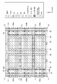
- FIG. 2 is a plan view showing the layout of IO cells in the first embodiment; 5 is a plan view showing some layers of FIG. 4; FIG. 5 is a plan view showing some layers of FIG. 4; FIG. (a) to (c) are cross-sectional structures of the layout in FIG. FIG.
- FIG. 2 is a plan view showing the layout of IO cells in the first embodiment; Circuit diagram of the output circuit in the modified example A plan view showing a layout of an IO cell in a modified example A plan view showing a layout of an IO cell in a modified example Overall configuration of a semiconductor integrated circuit device according to the second embodiment A plan view showing the layout of IO cells in the second embodiment.
- a plan view showing some layers of FIG. 13 A plan view showing some layers of FIG. 13 A plan view showing some layers of FIG. 13 (a) to (c) are cross-sectional structures of the layout of FIG.
- FIG. 4 is a plan view showing the layout of IO cells in Configuration Example 1 of the third embodiment; 20 is a plan view showing some layers of FIG.
- FIG. 11 is a plan view showing the layout of IO cells in configuration example 2 of the third embodiment
- 24 is a plan view showing some layers of FIG. 23
- FIG. 23 Modification of the configuration of FIG. FIG. 11 is a plan view showing the layout of IO cells in configuration example 2 of the third embodiment
- Modification of the configuration of FIG. FIG. 11 is a plan view showing the layout of IO cells in Configuration Example 3 of the third embodiment
- FIG. 11 is a plan view showing the layout of IO cells in Configuration Example 3 of the third embodiment;
- VSS and VDDIO refer to both the power supply itself or the power supply voltage.
- FIG. 1 is a plan view schematically showing the overall configuration of a semiconductor integrated circuit device (semiconductor chip) according to an embodiment.
- the horizontal direction of the drawing is the X direction
- the vertical direction of the drawing is the Y direction (the same applies to subsequent figures).
- a semiconductor integrated circuit device 1 shown in FIG. 1 includes a core region 2 in which an internal core circuit is formed, and an IO region 3 provided around the core region 2 and in which an interface circuit (IO circuit) is formed.
- An IO cell row 5 is provided in the IO region 3 so as to surround the core region 2 in the peripheral portion of the semiconductor integrated circuit device 1 .
- the IO cell column 5 includes a plurality of IO cells 10 forming an interface circuit.
- the IO cell 10 includes a signal IO cell for inputting, outputting or inputting/outputting a signal, a power supply IO cell for supplying a ground potential (power supply voltage VSS), and a power supply (power supply voltage VSS) mainly for the IO area 3.
- VDDIO is 1.8V.
- an IO cell 10A for signal input/output is arranged on the upper side of the core region 2 in the drawing, and an IO cell 10B for signal input/output is arranged on the left side of the core region 2 in the drawing.
- the IO area 3 is provided with power supply wirings 6 and 7 extending in the direction in which the IO cells 10 are arranged.
- the power supply wirings 6 and 7 are formed in a ring shape on the periphery of the semiconductor integrated circuit device 1 (also called ring power supply wiring).
- the power wiring 6 supplies VDDIO
- the power wiring 7 supplies VSS.
- the semiconductor integrated circuit device 1 is provided with a plurality of external connection pads.
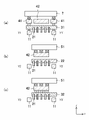
- FIG. 2 is a simplified configuration diagram of the IO cells 10A and 10B.
- the IO cell 10A has power supply wirings 6 and 7 extending in the X direction.
- an N conductivity type output transistor section 101 is provided under the power supply line 7 and a P conductivity type output transistor section 102 is provided under the power supply line 6 .
- the N-conductivity type output transistor section 101 and the P-conductivity type output transistor section 102 are provided outside the chip in the IO cell 10A.
- power supply wirings 6 and 7 extending in the Y direction are arranged in the IO cell 10B.
- an N conductivity type output transistor section 103 is provided under the power supply line 7 and a P conductivity type output transistor section 104 is provided under the power supply line 6 .
- the N-conductivity type output transistor section 103 and the P-conductivity type output transistor section 104 are provided outside the chip in the IO cell 10B.
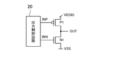
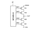
- FIG. 3 is a circuit diagram of the output circuit in this embodiment.
- a P-conductivity type (hereinafter referred to as P-type) transistor P1 is provided between a power supply VDDIO and an output terminal (which outputs an output signal OUT).
- a transistor N1 of N-conductivity type (hereinafter referred to as N-type as appropriate) is provided between it and the signal line.
- the output control circuit 20 outputs output control signals INP and INN.
- the transistor P1 receives an output control signal INP at its gate, and the transistor N1 receives an output control signal INN at its gate.
- An output signal OUT is supplied to an external connection pad.
- the output control signals INP and INN are at low level, the output signal OUT is at high level (VDDIO), and when the output control signals INP and INN are at high level, the output signal OUT is at low level (VSS).
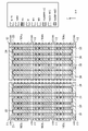
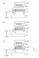
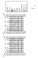
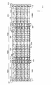
- FIG. 4 is a plan view showing the layout of the output transistor section in the IO cell 10B shown in FIG. 2(b) in this embodiment.
- 5 and 6 are plan views showing FIG. 4 divided into layers, FIG. 5 showing the configuration of the local wiring and lower layers, and FIG. 6 showing the configuration of the local wiring and higher layers.
- show. 7A and 7B are cross-sectional views showing the cross-sectional structure of the layout of FIG. The cross-sectional structure of Y3' is shown.
- the left portion of the drawing corresponds to the N conductivity type output transistor section 103 forming the transistor N1, and the right portion of the drawing corresponds to the P conductivity type output transistor section 104 forming the transistor P1.
- Fin FETs Field Effect Transistors
- the power wirings 6 and 7 shown in FIG. 2B are formed in the M2 wiring layer.
- the power supply wiring 7 for supplying VSS is provided on the N-conductivity type output transistor section 103
- the power supply wiring 6 for supplying VDDIO is provided on the P-conductivity type output transistor section 104 .
- the N conductivity type output transistor section 103 has three sections 103a, 103b, and 103c each having five fins 21 extending in parallel in the X direction.
- Embedded power supply wirings 11 extending in the X direction are arranged above and below the portions 103a, 103b, and 103c.
- the embedded power supply wiring 11 supplies VSS.
- a gate line 22 extending in the Y direction is arranged over portions 103a, 103b and 103c.
- a FinFET is formed by the Fin 21 and the gate wiring 22 .
- a local wiring 31 extending in the Y direction is commonly connected to the terminals of the fins 21 serving as the sources of the FinFETs.
- the local wiring 31 is connected to the embedded power supply wiring 11 through vias, and supplies VSS to the source of the FinFET.
- a local wiring 32 extending in the Y direction is commonly connected to terminals of the fins 21 serving as drains of the FinFETs.
- the local wiring 31 is connected via vias to the M1 wiring 41 extending in the X direction.
- the M1 wiring 41 is arranged at a position overlapping the embedded power supply wiring 11 in plan view.
- the M1 wiring 41 is connected via a via to the power supply wiring 7 formed in the M2 wiring layer.
- the local wiring 32 is connected via a via to the M1 wiring 42 extending in the X direction.
- the M1 wiring 42 is connected to the M2 wiring 51 via vias.
- the M1 wiring 42 and the M2 wiring 51 correspond to output wirings.
- the M2 wiring 51 is connected to an upper layer pad electrode (not shown).
- the configuration of the P-conductivity type output transistor section 104 is also substantially the same as that of the N-conductivity type output transistor section 103 .
- the P conductivity type output transistor section 104 has three sections 104a, 104b and 104c each having five fins 23 extending in parallel in the Y direction.
- Embedded power supply wirings 12 extending in the X direction are arranged above and below the portions 104a, 104b, and 104c in the drawing.
- the embedded power wiring 12 supplies VDDIO.
- a gate line 24 extending in the Y direction is arranged across portions 104a, 104b and 104c.
- a FinFET is formed by the Fin 23 and the gate wiring 24 .
- a local wiring 33 extending in the Y direction is commonly connected to the terminals of the fins 23 serving as the sources of the FinFETs.
- the local wiring 33 is connected to the embedded power supply wiring 12 via vias and supplies VDDIO to the source of the FinFET.
- a local wiring 34 extending in the Y direction is commonly connected to terminals of the fins 23 serving as drains of the FinFETs.
- the local wiring 33 is connected via vias to the M1 wiring 43 extending in the X direction.
- the M1 wiring 43 is arranged at a position overlapping the embedded power supply wiring 12 in plan view.
- the M1 wiring 43 is connected via a via to the power supply wiring 6 formed in the M2 wiring layer.
- the local wiring 34 is connected to the M1 wiring 42 extending in the X direction via vias.
- the power supply wiring for supplying VSS the power supply wiring 11 is formed in the embedded wiring layer, the power supply wiring 41 is formed in the M1 wiring layer, and the power supply wiring 7 is formed in the M2 wiring layer. .
- the resistance value of the VSS supply path is lowered, so that the power supply wirings 7 and 41 can be thinned.
- the power supply wirings for supplying VDDIO the power supply wiring 12 is formed in the embedded wiring layer, the power supply wiring 43 is formed in the M1 wiring layer, and the power supply wiring 6 is formed in the M2 wiring layer.
- the resistance value of the VDDIO supply path is lowered, so that the power supply wirings 6 and 43 can be thinned.
- the output wiring 42 of the M1 wiring layer and the output wiring 51 of the M2 wiring layer can be thickened while suppressing an increase in the area of the output circuit. Therefore, a large current can flow through the output terminal.
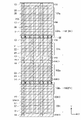
- FIG. 8 is a plan view showing the layout of the output transistor section in the IO cell 10A shown in FIG. 2(a). Note that the cross-sectional structure can be easily analogized from FIG. 7, and the illustration is omitted here.
- the upper portion of the drawing corresponds to the N conductivity type output transistor section 101 forming the transistor N1, and the lower portion of the drawing corresponds to the P conductivity type output transistor section 102 forming the transistor P1.
- Fin FETs are formed in the N conductivity type output transistor section 101 and the P conductivity type output transistor section 102 .
- the power wirings 6 and 7 shown in FIG. 2A are formed in the M1 wiring layer.
- the power supply wiring 7 for supplying VSS is provided on the N-conductivity type output transistor section 101
- the power supply wiring 6 for supplying VDDIO is provided on the P-conductivity type output transistor section 102 .
- the N conductivity type output transistor section 101 has three sections 101a, 101b, and 101c each having five fins 21 extending in parallel in the X direction.
- Embedded power supply wirings 13 extending in the X direction are arranged above and below the portions 101a, 101b, and 101c.
- the embedded power supply wiring 13 supplies VSS.
- a gate line 22 extending in the Y direction is arranged over portions 101a, 101b and 101c.
- a FinFET is formed by the Fin 21 and the gate wiring 22 .
- a local wiring 35 extending in the Y direction is commonly connected to the terminal of the fin 21 serving as the source of the FinFET.
- the local wiring 35 is connected to the embedded power supply wiring 13 through vias, and supplies VSS to the source of the FinFET.
- the local wiring 35 corresponds to power supply wiring.
- the local wiring 35 is connected via a via to the power supply wiring 7 formed in the M1 wiring layer.
- the P-conductivity type output transistor section 102 has three sections 102a, 102b, and 102c in which five fins 23 extending in parallel in the X direction are arranged.
- Embedded power supply wirings 14 extending in the X direction are arranged above and below the portions 102a, 102b, and 102c.
- the embedded power supply wiring 14 supplies VDDIO.
- a gate line 24 extending in the Y direction is arranged across portions 102a, 102b and 102c.
- a FinFET is formed by the Fin 23 and the gate wiring 24 .
- a local wiring 37 extending in the Y direction is commonly connected to the terminals of the fins 23 serving as the sources of the FinFETs.
- the local wiring 37 is connected to the embedded power supply wiring 14 via vias and supplies VDDIO to the source of the FinFET.
- the local wiring 37 corresponds to power supply wiring.
- the local wiring 37 is connected via vias to the power supply wiring 6 formed in the M1 wiring layer.
- a terminal of the fin 21 serving as the drain of the FinFET in the N-conductivity output transistor section 101 and a terminal of the fin 23 serving as the drain of the FinFET in the P-conductivity output transistor section 102 share a local wiring 36 extending in the Y direction. It is connected to the.
- the local wiring 36 is connected to the M1 wiring 45 via vias. Local wiring 36 and M1 wiring 45 correspond to output wiring.
- the M1 wiring 45 is connected to an upper layer pad electrode (not shown).
- the power supply wiring 13 is formed in the embedded wiring layer, the local wiring 35 is formed, and the power supply wiring 7 is formed in the M1 wiring layer as the power supply wiring for supplying VSS.
- the resistance value of the VSS supply path is lowered, so that the power supply wiring 7 can be thinned.
- the power supply wiring 14 is formed in the embedded wiring layer, the local wiring 37 is formed, and the power supply wiring 6 is formed in the M1 wiring layer.
- the resistance value of the VDDIO supply path is reduced, so that the power supply wiring 6 can be thinned.
- the output wiring 45 of the M1 wiring layer can be thickened while suppressing an increase in the area of the output circuit. Therefore, a large current can flow through the output terminal.
- an embedded power supply wiring 13 supplying VSS and an embedded power supply wiring 14 supplying VDDIO are formed between the transistor N1 and the transistor P1. Since the embedded power supply wiring is formed by embedding metal wiring in grooves provided in the substrate, wells in the substrate, STI, etc., it has the effect of reducing noise propagation through the substrate and the like. Therefore, by providing a buried power supply wiring between transistors N1 and P1, latch-up resistance can be improved.
- FIG. 9 is a circuit diagram of an output circuit in a modification.
- P-type transistors P21 and P22 are provided in series between the power supply VDDIO and the output signal line, and N-type transistors N21 and P22 are provided between the power supply VSS and the output signal line. N22 are arranged in series.
- the output control circuit 21 outputs output control signals INP1, INP2, INN1 and INN2.
- Transistor P21 receives output control signal INP1 at its gate, and transistor P22 receives output control signal INP2 at its gate.
- Transistor N21 receives output control signal INN1 at its gate, and transistor N22 receives output control signal INN2 at its gate.
- the output signal OUT is then supplied to an external connection pad.
- the output control signals INP1, INP2, INN1 and INN2 are at low level, the output signal OUT is at high level (VDDIO), and when the output control signals INP1, INP2, INN1 and INN2 are at high level, the output signal OUT is at low level. (VSS).
- One of the output control signals INP1 and INP2 may be at the fixed potential (VSS) and one of the output control signals INN1 and INN2 may be at the fixed potential (VDDIO).
- FIG. 10 is a plan view showing the layout of the output transistor section in the IO cell 10B shown in FIG. 2(b) according to this modification.
- the left portion of the drawing corresponds to the N conductivity type output transistor section 103 that constitutes the transistors N21 and N22
- the right portion of the drawing corresponds to the P conductivity type output transistor section 104 that constitutes the transistors P21 and P22. do.
- Fin FETs are formed in the N conductivity type output transistor section 103 and the P conductivity type output transistor section 104 .
- the power wirings 6 and 7 shown in FIG. 2B are formed in the M2 wiring layer.
- the power supply wiring 7 for supplying VSS is provided on the N-conductivity type output transistor section 103
- the power supply wiring 6 for supplying VDDIO is provided on the P-conductivity type output transistor section 104 .
- the layout of FIG. 10 has a longer fin length because the transistors are arranged in series in two stages, and two gate wirings are arranged between the local wirings.
- the basic configuration is the same as that of the above-described embodiment, and detailed description will be omitted.
- the M1 wiring 44 is connected to the M2 wiring 52, and the M2 wiring 52 is connected to an upper layer pad electrode (not shown).
- FIG. 11 is a plan view showing the layout of the output transistor section in the IO cell 10A shown in FIG. 2(a) in this modification.
- the upper portion of the drawing corresponds to the N conductivity type output transistor section 101 forming the transistors N21 and N22
- the lower portion of the drawing corresponds to the P conductivity type output transistor section 102 forming the transistors P21 and P22.
- Fin FETs are formed in the N conductivity type output transistor section 101 and the P conductivity type output transistor section 102 .
- the power wirings 6 and 7 shown in FIG. 2B are formed in the M1 wiring layer.
- the power supply wiring 7 for supplying VSS is provided on the N-conductivity type output transistor section 101
- the power supply wiring 6 for supplying VDDIO is provided on the P-conductivity type output transistor section 102 .
- the layout of FIG. 11 has two tiers of transistors in series, so the length of the fin is longer, and two gate wirings are arranged between the local wirings.
- the basic configuration is the same as that of the above-described embodiment, and detailed description will be omitted.
- the M1 wiring 46 is connected to an upper layer pad electrode (not shown).
- the same effects as those of the above-described embodiment can be obtained. That is, in the layout of FIG. 10, the output wiring 44 of the M1 wiring layer and the output wiring 52 of the M2 wiring layer can be thickened while suppressing an increase in the area of the output circuit. Therefore, a large current can flow through the output terminal. In the layout of FIG. 11, the output wiring 46 of the M1 wiring layer can be thickened while suppressing an increase in the area of the output circuit. Therefore, a large current can flow through the output terminal.
- an embedded power supply wiring for supplying VSS and an embedded power supply wiring for supplying VDDIO are formed between the transistor N1 and the transistor P1. Since the embedded power supply wiring is formed by embedding metal wiring in grooves provided in the substrate, wells in the substrate, STI, etc., it has the effect of reducing noise propagation through the substrate and the like. Therefore, by providing a buried power supply wiring between transistors N1 and P1, latch-up resistance can be improved.
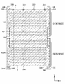
- FIG. 12 is a diagram showing the overall configuration of a semiconductor integrated circuit device according to the second embodiment.
- a semiconductor integrated circuit device 200 is configured by stacking a first semiconductor chip 201 (chip A) and a second semiconductor chip 202 (chip B). In the stacked portion, the back surface of the first semiconductor chip 201 and the main surface of the second semiconductor chip 202 face each other.
- the first semiconductor chip 201 is formed with a circuit including a transistor that constitutes an output buffer, and is also formed with an embedded power supply wiring.
- the second semiconductor chip 202 has power supply wirings connected to embedded power supply wirings formed in the first semiconductor chip 201 .
- the embedded power wiring formed in the first semiconductor chip 201 and the power wiring formed in the second semiconductor chip 202 are connected via a through silicon via (TSV).
- TSV through silicon via
- the plan view of the semiconductor integrated circuit device 200 shown in FIG. 12 is the same as in FIG. That is, the first semiconductor chip 201 includes a core region 2 in which an internal core circuit is formed, and an IO region 3 provided around the core region 2 and in which an interface circuit (IO circuit) is formed.
- An IO cell array 5 is provided in the IO region 3 so as to surround the core region 2 in the peripheral portion of the semiconductor integrated circuit device 200 .
- a plurality of IO cells 10 forming an interface circuit are arranged in the IO cell column 5 .
- the power wirings 6 and 7 extending in the direction in which the IO cells 10 are arranged are formed on the second semiconductor chip 202 .
- the simple configuration of the IO cells 10A and 10B is the same as in FIG. 2, and the circuit diagram of the output circuit is the same as in FIG.
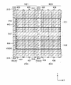
- FIG. 13 is a plan view showing the layout of the output transistor section in the IO cell 10B shown in FIG. 2(b) in this embodiment.
- the layout of FIG. 13 corresponds to the circuit diagram of FIG. 14 to 16 are plan views showing FIG. 13 divided into layers.
- 14 shows the configuration of the power supply wiring of the second semiconductor chip 202 and the embedded power supply wiring and fins of the first semiconductor chip 201
- FIG. FIG. 16 shows the configuration of the local wiring of the first semiconductor chip 201 and the upper layers.
- 17A and 17B are cross-sectional views showing the cross-sectional structure of the layout of FIG. The cross-sectional structure of Y3' is shown.
- the left portion of the drawing corresponds to the N conductivity type output transistor portion 103 forming the transistor N1, and the right portion of the drawing corresponds to the P conductivity type output transistor portion 104 forming the transistor P1.
- Fin FETs Field Effect Transistors
- the power wirings 6 and 7 shown in FIG. 2B are formed on the second semiconductor chip 202 .
- the power supply wiring 7 for supplying VSS is provided at a position overlapping with the N-conductivity type output transistor section 103 in plan view
- the power supply wiring 6 for supplying VDDIO is provided at a position overlapping with the P-conductivity type output transistor section 104 in plan view. It is
- the N conductivity type output transistor section 103 has three sections 103a, 103b, and 103c each having five fins 21 extending in parallel in the X direction.
- Embedded power supply wirings 11 extending in the X direction are arranged above and below the portions 103a, 103b, and 103c in the drawing.
- the embedded power supply wiring 11 supplies VSS.
- the embedded power supply wiring 11 is connected to the power supply wiring 7 of the second semiconductor chip 202 via the TSV.
- a gate wiring 22 extending in the Y direction is arranged over the portions 103a, 103b, and 103c.
- a FinFET is formed by the Fin 21 and the gate wiring 22 .
- a local wiring 31 extending in the Y direction is commonly connected to the terminal of the fin 21 serving as the source of the FinFET.
- the local wiring 31 is connected to the embedded power supply wiring 11 through vias, and supplies VSS to the source of the FinFET.
- a local wiring 32 extending in the Y direction is commonly connected to terminals of the fins 21 serving as drains of the FinFETs.
- the local wiring 32 is connected via a via to the M1 wiring 242 extending in the X direction.
- the M1 wiring 242 is connected to the M2 wiring 251 through vias 261 .
- the M1 wiring 242 and the M2 wiring 251 correspond to output wirings.
- the M2 wiring 251 is connected to an upper layer pad electrode (not shown).
- the P-conductivity type output transistor section 104 has three sections 104a, 104b, and 104c each having five fins 23 extending in parallel in the X direction.
- Embedded power supply wirings 12 extending in the X direction are arranged above and below the portions 104a, 104b, and 104c in the drawing.
- the embedded power wiring 12 supplies VDDIO.
- the embedded power wiring 12 is connected to the power wiring 6 of the second semiconductor chip 202 via the TSV.
- a gate wiring 24 extending in the Y direction is arranged over the portions 104a, 104b, and 104c.
- a FinFET is formed by the Fin 23 and the gate wiring 24 .
- a local wiring 33 extending in the Y direction is commonly connected to the terminals of the fins 23 serving as the sources of the FinFETs.
- the local wiring 33 is connected to the embedded power supply wiring 12 via vias and supplies VDDIO to the source of the FinFET.
- a local wiring 34 extending in the Y direction is commonly connected to terminals of the fins 23 serving as drains of the FinFETs.
- the local wiring 34 is connected via a via to the M1 wiring 242 extending in the X direction.
- the power wirings 6 and 7 of the second semiconductor chip 202 overlap the M2 wirings 251 of the first semiconductor chip 201 in plan view. Also, the arrangement position of the via 261 connecting the M1 wiring 242 and the M2 wiring 251 overlaps with the power supply wirings 6 and 7 of the second semiconductor chip 202 in plan view.
- the power wiring 11 formed in the embedded wiring layer of the first semiconductor chip 201 and the power wiring 7 formed in the second semiconductor chip 202 are formed as power wiring for supplying VSS. ing.
- the resistance value of the VSS supply path can be reduced without providing the power wiring in the M1 wiring layer of the first semiconductor chip 201 .
- power supply wirings for supplying VDDIO power supply wirings 12 formed in the embedded wiring layer of the first semiconductor chip 201 and power supply wirings 6 formed in the second semiconductor chip 202 are formed.
- the resistance value of the VDDIO supply path can be reduced without providing the power wiring in the M1 wiring layer of the first semiconductor chip 201 .
- the output wiring 242 of the M1 wiring layer and the output wiring 251 of the M2 wiring layer can be thickened, and the number of vias 261 connecting them can be increased.
- a large current can flow through the
- the power supply wirings 6 and 7 formed on the second semiconductor chip 202 also overlap the output wiring 251 in a plan view, and can be made thicker.
- FIG. 18 is a plan view showing the layout of the output transistor section in the IO cell 10A shown in FIG. 2(a) in this embodiment. Note that the cross-sectional structure can be easily analogized from FIG. 17, and the illustration is omitted here.
- the upper portion of the drawing corresponds to the N conductivity type output transistor section 101 forming the transistor N1, and the lower portion of the drawing corresponds to the P conductivity type output transistor section 102 forming the transistor P1.
- Fin FETs are formed in the N conductivity type output transistor section 101 and the P conductivity type output transistor section 102 .
- the power wirings 6 and 7 shown in FIG. 2A are formed on the second semiconductor chip 202 .
- the power wiring 7 for supplying VSS is provided at a position overlapping with the N-conductivity type output transistor section 101 in plan view
- the power wiring 6 for supplying VDDIO is provided at a position overlapping with the P-conductivity type output transistor section 102 in plan view. It is
- the N conductivity type output transistor section 101 has three sections 101a, 101b, and 101c each having five fins 21 extending in parallel in the X direction.
- Embedded power supply wirings 13 extending in the X direction are arranged above and below the portions 101a, 101b, and 101c in the drawing.
- the embedded power supply wiring 13 supplies VSS.
- the embedded power supply wiring 13 is connected to the power supply wiring 7 of the second semiconductor chip 202 via the TSV.
- a gate wiring 22 extending in the Y direction is arranged over the portions 101a, 101b, and 101c.
- a FinFET is formed by the Fin 21 and the gate wiring 22 .
- a local wiring 35 extending in the Y direction is commonly connected to the terminals of the fins 21 serving as the sources of the FinFETs.
- the local wiring 35 is connected to the embedded power supply wiring 13 through vias, and supplies VSS to the source of the FinFET.
- the P-conductivity type output transistor section 102 has three sections 102a, 102b, and 102c in which five fins 23 extending in parallel in the X direction are arranged.
- Embedded power supply wirings 14 extending in the X direction are arranged above and below the portions 102a, 102b, and 102c in the drawing.
- the embedded power supply wiring 14 supplies VDDIO.
- the embedded power supply wiring 14 is connected to the power supply wiring 6 of the second semiconductor chip 202 via the TSV.
- a gate wiring 24 extending in the Y direction is arranged over the portions 102a, 102b, and 102c.
- a FinFET is formed by the Fin 23 and the gate wiring 24 .
- a local wiring 37 extending in the Y direction is commonly connected to the terminals of the fins 23 serving as the sources of the FinFETs.
- the local wiring 37 is connected to the embedded power supply wiring 14 via vias and supplies VDDIO to the source of the FinFET.
- a terminal of the fin 21 serving as the drain of the FinFET in the N-conductivity output transistor section 101 and a terminal of the fin 23 serving as the drain of the FinFET in the P-conductivity output transistor section 102 share a local wiring 36 extending in the Y direction. It is connected to the. Local wiring 36 is connected to M1 wiring 245 via via 262 . Local wiring 36 and M1 wiring 245 correspond to output wiring. The M1 wiring 245 is connected to an upper layer pad electrode (not shown).
- the power wirings 6 and 7 of the second semiconductor chip 202 overlap the M1 wirings 245 of the first semiconductor chip 201 in plan view. Also, the arrangement position of the via 262 connecting the local wiring 36 and the M1 wiring 245 overlaps with the power supply wirings 6 and 7 of the second semiconductor chip 202 in plan view.
- the power wiring 13 formed in the embedded wiring layer of the first semiconductor chip 201 and the power wiring 7 formed in the second semiconductor chip 202 are formed as the power wiring for supplying VSS. ing.
- the resistance value of the VSS supply path can be lowered without providing the power wiring in the M1 wiring layer of the first semiconductor chip 201 .
- the power supply wirings 14 formed in the embedded wiring layer of the first semiconductor chip 201 and the power supply wirings 6 formed in the second semiconductor chip 202 are formed.
- the resistance value of the VDDIO supply path can be reduced without providing the power wiring in the M1 wiring layer of the first semiconductor chip 201 .
- the output wiring 245 of the M1 wiring layer can be thickened, and the number of vias 262 for connecting to the local wiring 36 can be increased, so that a large current can flow to the output terminal. can flow.
- the power supply wirings 6 and 7 formed on the second semiconductor chip 202 also overlap the output wiring 245 in a plan view, and can be made thicker.
- the power supply wirings 6 and 7 formed on the second semiconductor chip 202 may be of a single layer or may be of multiple layers.
- the wiring direction is not limited to the one shown here.
- each layer may be extended in a direction perpendicular to each other to form a mesh-like power wiring. This makes it possible to further strengthen the power supply.
- both the VSS power supply wiring and the VDDIO power supply wiring are formed on the second semiconductor chip 202, but only one of the power supply wirings may be formed on the second semiconductor chip 202. .
- the output transistor has a two-stage configuration, it can be similarly configured.
- the BPR that is, the power supply wiring formed in the embedded wiring layer extends in the X direction.
- the BPR extends in the Y direction.
- Configuration example 1 corresponds to the first embodiment.
- the circuit configuration of the output circuit is as shown in the circuit diagram of FIG.
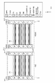
- FIG. 19 is a plan view showing the layout of the output transistor section in the IO cell 10B shown in FIG. 2(b) in this configuration example.
- 20 and 21 are plan views showing FIG. 19 divided into layers, FIG. 20 showing the configuration of the local wiring and lower layers, and FIG. 21 showing the configuration of the local wiring and higher layers.
- show. 19 to 21 are diagrams corresponding to FIGS. 4 to 6 shown in the first embodiment, and explanations of configurations that can be easily guessed from the description of the first embodiment may be omitted.
- the left portion of the drawing corresponds to the N conductivity type output transistor portion 103 forming the transistor N1, and the right portion of the drawing corresponds to the P conductivity type output transistor portion 104 forming the transistor P1.
- Fin FETs Field Effect Transistors
- the power wirings 6 and 7 shown in FIG. 2B are formed in the M2 wiring layer.
- the power supply wiring 7 for supplying VSS is provided on the N-conductivity type output transistor section 103
- the power supply wiring 6 for supplying VDDIO is provided on the P-conductivity type output transistor section 104 .
- an output wiring 51 is formed in the M2 wiring layer.
- the M2 wiring 51 is connected to an upper layer pad electrode (not shown).
- the N conductivity type output transistor section 103 has ten fins 21 extending in parallel in the X direction.
- Embedded power supply wirings 311 extending in the Y direction are arranged on the left and right sides of the fin 21 in the drawing, respectively.
- the embedded power supply wiring 311 supplies VSS.
- a gate wiring 22 extending in the Y direction over ten fins 21 is arranged.
- a FinFET is formed by the Fin 21 and the gate wiring 22 .
- a local wiring 330 extending in the Y direction is formed in a layer above the embedded power supply wiring 311 so as to overlap the embedded power supply wiring 311 in a plan view.
- the local wiring 330 is connected to the underlying embedded power supply wiring 311 via vias.
- a local wiring 331 extending in the Y direction is commonly connected to the terminal of the fin 21 serving as the source of the FinFET.
- the local wiring 331 is connected to the local wiring 330 via five M1 wirings 341 extending in parallel in the X direction, and supplies VSS to the source of the FinFET.
- the M1 wiring 341 is connected via vias to the power supply wiring 7 formed in the M2 wiring layer.
- a local wiring 332 extending in the Y direction is commonly connected to the terminals of the fins 21 serving as the drains of the finFETs.
- the local wiring 332 is connected via a via to the M1 wiring 342 extending in parallel in the X direction.
- the M1 wiring 342 is connected to the M2 wiring 51 via vias.
- the configuration of the P-conductivity type output transistor section 104 is also substantially the same as that of the N-conductivity type output transistor section 103 .
- Ten fins 23 extending in parallel in the X direction are arranged in the P conductivity type output transistor section 104 .
- Embedded power supply wirings 312 extending in the Y direction are arranged on the left and right sides of the fin 23 in the drawing, respectively.
- the embedded power wiring 312 supplies VDDIO.
- a gate wiring 24 extending in the Y direction over ten fins 23 is arranged.
- a FinFET is formed by the Fin 23 and the gate wiring 24 .
- a local wiring 335 extending in the Y direction is formed on the upper layer of the embedded power supply wiring 312 so as to overlap with the embedded power supply wiring 312 in plan view.
- the local wiring 335 is connected to the underlying embedded power supply wiring 312 via vias.
- a local wiring 333 extending in the Y direction is commonly connected to the terminals of the fins 23 serving as the sources of the FinFETs.
- the local wiring 333 is connected to the local wiring 335 via five M1 wirings 343 extending in parallel in the X direction, and supplies VDDIO to the source of the FinFET.
- the M1 wiring 343 is connected via a via to the power supply wiring 6 formed in the M2 wiring layer.
- a local wiring 334 extending in the Y direction is commonly connected to the terminals of the fins 23 serving as the drains of the finFETs. Similar to the local wiring 332, the local wiring 334 is connected via vias to five M1 wirings 342 extending in parallel in the X direction.
- the power supply wiring for supplying VSS the power supply wiring 311 is formed in the embedded wiring layer, the local wiring 330 is formed, the power supply wiring 341 is formed in the M1 wiring layer, and the power supply wiring is formed in the M2 wiring layer.
- a wiring 7 is formed.
- the resistance value of the VSS supply path is lowered, so that the power supply wiring 7 can be thinned.
- a power supply wiring 312 is formed in the embedded wiring layer, a local wiring 335 is formed, a power supply wiring 343 is formed in the M1 wiring layer, and a power supply wiring 6 is formed in the M2 wiring layer.
- the resistance value of the VDDIO supply path is reduced, so that the power supply wiring 6 can be thinned.
- the output wiring 51 of the M2 wiring layer can be thickened while suppressing an increase in the area of the output circuit. Therefore, a large current can flow through the output terminal.
- an embedded power supply wiring 311 supplying VSS and an embedded power supply wiring 312 supplying VDDIO are formed between the transistor N1 and the transistor P1. Since the embedded power supply wiring is formed by embedding metal wiring in grooves provided in the substrate, wells in the substrate, STI, etc., it has the effect of reducing noise propagation through the substrate and the like. Therefore, by providing embedded power supply wirings 311 and 312 between transistors N1 and P1, latch-up resistance can be improved.
- FIG. 22 is a plan view showing the layout of the output transistor section in the IO cell 10A shown in FIG. 2(a) in this configuration example.
- FIG. 22 is a diagram corresponding to FIG. 8 shown in the first embodiment, and the description of the configuration that can be easily guessed from the description of the first embodiment may be omitted.
- the upper portion of the drawing corresponds to the N conductivity type output transistor section 101 forming the transistor N1, and the lower portion of the drawing corresponds to the P conductivity type output transistor section 102 forming the transistor P1.
- Fin FETs are formed in the N conductivity type output transistor section 101 and the P conductivity type output transistor section 102 .
- the power wirings 6 and 7 shown in FIG. 2A are formed in the M1 wiring layer.
- the power supply wiring 7 for supplying VSS is provided on the N-conductivity type output transistor section 101
- the power supply wiring 6 for supplying VDDIO is provided on the P-conductivity type output transistor section 102 .
- the N conductivity type output transistor section 101 has ten fins 21 extending in parallel in the X direction.
- Embedded power supply wirings 313 extending in the Y direction are arranged on the left and right sides of the fin 21 in the drawing, respectively.
- the embedded power supply wiring 313 supplies VSS.
- a gate wiring 22 extending in the Y direction over ten fins 21 is arranged.
- a FinFET is formed by the Fin 21 and the gate wiring 22 .
- a local wiring 336 extending in the Y direction is formed on the upper layer of the embedded power supply wiring 313 so as to overlap with the embedded power supply wiring 313 in plan view.
- the local wiring 336 is connected to the underlying embedded power supply wiring 313 via vias. Also, the local wiring 336 is connected to the power supply wiring 7 formed in the upper M1 wiring layer through vias.
- a local wiring 337 extending in the Y direction is commonly connected to the terminal of the fin 21 serving as the source of the FinFET.
- the local wiring 337 is connected to the power supply wiring 7 formed in the M1 wiring layer via vias, and supplies VSS to the source of the FinFET.
- the P-type output transistor section 102 has ten fins 23 extending in parallel in the X direction.
- Embedded power supply wirings 314 extending in the Y direction are arranged on the left and right sides of the fin 23 in the drawing, respectively.
- the embedded power wiring 314 supplies VDDIO.
- a gate wiring 24 extending in the Y direction over ten fins 23 is arranged.
- a FinFET is formed by the Fin 23 and the gate wiring 24 .
- a local wiring 340 extending in the Y direction is formed in a layer above the embedded power supply wiring 314 so as to overlap the embedded power supply wiring 314 in a plan view.
- the local wiring 340 is connected to the underlying embedded power supply wiring 314 via vias. Also, the local wiring 340 is connected to the power supply wiring 6 formed in the upper M1 wiring layer through vias.
- a local wiring 338 extending in the Y direction is commonly connected to the terminals of the fins 23 serving as the sources of the FinFETs.
- the local wiring 338 is connected to the power supply wiring 6 formed in the M1 wiring layer via vias, and supplies VDDIO to the source of the FinFET.
- a local wiring 339 extending in the Y direction is common to the terminal of the fin 21 serving as the drain of the FinFET in the N-conductivity output transistor section 101 and the terminal of the fin 23 serving as the drain of the FinFET in the P-conductivity output transistor section 102 . It is connected to the.
- the local wiring 339 is connected via a via to the output wiring 45 formed in the M1 wiring layer.
- the M1 wiring 45 is connected to an upper layer pad electrode (not shown).
- the power supply wiring for supplying VSS the power supply wiring 313 is formed in the embedded wiring layer, the local wirings 336 and 337 are formed, and the power supply wiring 7 is formed in the M1 wiring layer.
- the resistance value of the VSS supply path is lowered, so that the power supply wiring 7 can be thinned.
- a power supply wiring 314 is formed in the embedded wiring layer, local wirings 338 and 340 are formed, and a power supply wiring 6 is formed in the M1 wiring layer.
- the resistance value of the VDDIO supply path is reduced, so that the power supply wiring 6 can be thinned.
- the output wiring 45 of the M1 wiring layer can be thickened while suppressing an increase in the area of the output circuit. Therefore, a large current can flow through the output terminal.
- Configuration example 2 corresponds to the circuit diagram of FIG. 9 according to the modification of the first embodiment
- Configuration example 2 corresponds to a modification of the first embodiment.
- the circuit configuration of the output circuit is as shown in the circuit diagram of FIG.
- FIG. 23 is a plan view showing the layout of the output transistor section in the IO cell 10B shown in FIG. 2(b) in this configuration example.
- 24 and 25 are plan views showing FIG. 23 divided into layers, FIG. 24 showing the configuration of the local wiring and lower layers, and FIG. 25 showing the configuration of the local wiring and higher layers.
- show. 23 to 25 are diagrams corresponding to FIG. 10 shown in the modified example of the first embodiment, and the description of the configuration that can be easily guessed from the description of the modified example of the first embodiment may be omitted. be.
- the left portion of the drawing corresponds to the N conductivity type output transistor portion 103 forming the transistors N21 and N22, and the right portion of the drawing corresponds to the P conductivity type output transistor portion forming the transistors P21 and P22.
- Fin FETs are formed in the N conductivity type output transistor section 103 and the P conductivity type output transistor section 104 .
- the power wirings 6 and 7 shown in FIG. 2B are formed in the M2 wiring layer.
- the power supply wiring 7 for supplying VSS is provided on the N-conductivity type output transistor section 103
- the power supply wiring 6 for supplying VDDIO is provided on the P-conductivity type output transistor section 104 .
- an output wiring 52 is formed in the M2 wiring layer.
- the M2 wiring 52 is connected to an upper layer pad electrode (not shown).
- the layouts of FIGS. 23 to 25 have longer fins because the transistors are arranged in series in two stages, and two gate wirings are provided between the local wirings. are placed.
- the basic configuration is the same as that of configuration example 1 described above, and detailed description thereof will be omitted.
- the output wiring 52 of the M2 wiring layer can be thickened while suppressing an increase in the area of the output circuit. Therefore, a large current can flow through the output terminal.
- FIG. 26 is a modified example of the configuration of FIG.
- the series-connected transistors N21 and N22 are configured by a single fin, and the serially-connected transistors P21 and P22 are configured by a single fin.
- the fins forming the transistor N21 and the fins forming the transistor N22 are separated, and the fins forming the transistor P21 and the fin forming the transistor P22 are separated. ing. That is, the transistor N21 and the transistor N22 are configured independently of each other, and the structures forming the channel, gate, source and drain are separated from each other. Further, the transistor P21 and the transistor P22 are configured independently of each other, and the structures forming the channel, gate, source and drain are separated from each other.
- an embedded power supply wiring 311 is formed between the transistor N21 and the transistor N22.
- a local wiring 431 connected to a terminal serving as the drain of the fin of the transistor N21 and a local wiring 432 connected to a terminal serving as the source of the fin of the transistor N22 are connected to each other. are connected via an M1 wiring 441 extending in the direction.
- an embedded power supply wiring 312 is formed between the transistor P21 and the transistor P22.
- a local wiring 433 connected to a terminal serving as the drain of the fin of the transistor P21 and a local wiring 434 connected to a terminal serving as the source of the fin of the transistor P22 are connected to each other. are connected via an M1 wiring 442 extending in the direction.
- the transistors N21 and N22 are formed by fins separated from each other, and the transistors P21 and P22 are formed by fins separated from each other. Thereby, the ESD resistance of the semiconductor integrated circuit device can be improved.
- FIG. 27 is a plan view showing the layout of the output transistor section in the IO cell 10A shown in FIG. 2(a) in this configuration example.
- FIG. 27 is a diagram corresponding to FIG. 11 showing the modified example of the first embodiment, and the description of the configuration that can be easily guessed from the description of the first embodiment may be omitted.
- the upper portion of the drawing corresponds to the N conductivity type output transistor section 101 forming the transistors N21 and N22
- the lower portion of the drawing corresponds to the P conductivity type output transistor section 102 forming the transistors P21 and P22.
- Fin FETs are formed in the N conductivity type output transistor section 101 and the P conductivity type output transistor section 102 .
- the power wirings 6 and 7 shown in FIG. 2B are formed in the M1 wiring layer.
- the power supply wiring 7 for supplying VSS is provided on the N-conductivity type output transistor section 101
- the power supply wiring 6 for supplying VDDIO is provided on the P-conductivity type output transistor section 102 .
- an output wiring 45 is formed in the M1 wiring layer.
- the output wiring 45 of the M1 wiring layer can be thickened while suppressing an increase in the area of the output circuit. Therefore, a large current can flow through the output terminal.
- FIG. 28 is a modified example of the configuration of FIG.
- the series-connected transistors N21 and N22 are configured by a series of fins
- the series-connected transistors P21 and P22 are configured by a series of fins.
- the fins forming the transistor N21 and the fins forming the transistor N22 are separated, and the fins forming the transistor P21 and the fin forming the transistor P22 are separated. ing. That is, the transistor N21 and the transistor N22 are configured independently of each other, and the structures forming the channel, gate, source and drain are separated from each other.
- the transistor P21 and the transistor P22 are configured independently of each other. The structures that make up the channel, gate, source and drain are isolated from each other.
- an embedded power supply wiring 313 is formed between the transistor N21 and the transistor N22.
- a local wiring 435 connected to a terminal serving as the drain of the fin of the transistor N21 and a local wiring 436 connected to a terminal serving as the source of the fin of the transistor N22 are connected to each other. are connected via an M1 wiring 443 extending in the direction.
- an embedded power supply wiring 314 is formed between the transistor P21 and the transistor P22. Then, a local wiring 437 connected to a terminal serving as the drain of the fin of the transistor P21 and a local wiring 438 connected to a terminal serving as the source of the fin of the transistor P22 are connected to each other. are connected via an M1 wiring 444 extending in the direction.
- the transistors N21 and N22 are formed by fins separated from each other, and the transistors P21 and P22 are formed by fins separated from each other. Thereby, the ESD resistance of the semiconductor integrated circuit device can be improved.
- Configuration example 3 corresponds to the above-described second embodiment.
- the overall configuration of the semiconductor integrated circuit device is as shown in FIG. 12, and the circuit configuration of the output circuit is as shown in the circuit diagram of FIG.
- FIG. 29 is a plan view showing the layout of the output transistor section in the IO cell 10B shown in FIG. 2(b) in the third configuration example.
- the layout of FIG. 29 corresponds to the circuit diagram of FIG. 30 to 32 are plan views showing FIG. 29 divided into layers.
- 30 shows the configuration of the power supply wiring of the second semiconductor chip 202 and the embedded power supply wiring and fins of the first semiconductor chip 201
- FIG. FIG. 32 shows the configuration of the local wiring of the first semiconductor chip 201 and the upper layers.
- 29 to 32 are diagrams corresponding to FIGS. 13 to 16 shown in the second embodiment, and explanations of configurations that can be easily guessed from the description of the second embodiment may be omitted.
- the left portion of the drawing corresponds to the N conductivity type output transistor portion 103 forming the transistor N1
- the right portion of the drawing corresponds to the P conductivity type output transistor portion 104 forming the transistor P1.
- Fin FETs Field Effect Transistors
- the power wirings 6 and 7 shown in FIG. 2B are formed on the second semiconductor chip 202 .
- the power supply wiring 7 for supplying VSS is provided at a position overlapping with the N-conductivity type output transistor section 103 in plan view, and the power supply wiring 6 for supplying VDDIO is provided at a position overlapping with the P-conductivity type output transistor section 104 in plan view. It is
- the N conductivity type output transistor section 103 has ten fins 21 extending in parallel in the X direction.
- Embedded power supply wirings 511 extending in the Y direction are arranged on the left and right sides of the fin 21 in the drawing.
- An embedded power supply wiring 511 supplies VSS.
- the embedded power wiring 511 is connected to the power wiring 7 of the second semiconductor chip 202 via the TSV.
- a gate wiring 22 extending in the Y direction over ten fins 21 is arranged.
- a FinFET is formed by the Fin 21 and the gate wiring 22 .
- a local wiring 530 extending in the Y direction is formed on the upper layer of the embedded power supply wiring 511 so as to overlap with the embedded power supply wiring 511 in plan view.
- the local wiring 530 is connected to the underlying embedded power supply wiring 511 via vias.
- a local wiring 531 extending in the Y direction is commonly connected to the terminals of the fins 21 serving as the sources of the FinFETs.
- the local wiring 531 is connected to the local wiring 530 via the M1 wiring 541 extending in the X direction, and supplies VSS to the source of the FinFET.
- a local wiring 532 extending in the Y direction is commonly connected to the terminals of the fins 21 serving as the drains of the finFETs.
- the local wiring 532 is connected via a via to the M1 wiring 542 extending in the X direction.
- the M1 wiring 542 is connected to the M2 wiring 551 through vias 561 .
- the M1 wiring 542 and the M2 wiring 551 correspond to output wirings.
- the M2 wiring 551 is connected to an upper layer pad electrode (not shown).
- the P-conductivity type output transistor section 104 has ten fins 23 extending in parallel in the X direction.
- Embedded power supply wirings 512 extending in the Y direction are arranged on the left and right sides of the fin 23 in the drawing.
- the embedded power supply wiring 512 supplies VDDIO.
- the embedded power supply wiring 512 is connected to the power supply wiring 6 of the second semiconductor chip 202 via the TSV.
- a gate wiring 24 extending in the Y direction over ten fins 23 is arranged.
- a FinFET is formed by the Fin 23 and the gate wiring 24 .
- a local wiring 535 extending in the Y direction is formed in a layer above the embedded power supply wiring 512 so as to overlap the embedded power supply wiring 512 in plan view.
- the local wiring 535 is connected to the underlying embedded power supply wiring 512 via vias.
- a local wiring 533 extending in the Y direction is commonly connected to the terminal of the fin 23 serving as the source of the FinFET.
- the local wiring 533 is connected to the local wiring 535 via the M1 wiring 543 extending in the X direction, and supplies VDDIO to the source of the FinFET.
- a local wiring 534 extending in the Y direction is commonly connected to the terminals of the fins 23 serving as the drains of the finFETs.
- the local wiring 534 is connected via a via to the M1 wiring 542 extending in the X direction.
- the power wirings 6 and 7 of the second semiconductor chip 202 overlap the M2 wirings 551 of the first semiconductor chip 201 in plan view. Also, the arrangement position of the via 561 connecting the M1 wiring 542 and the M2 wiring 551 overlaps with the power supply wirings 6 and 7 of the second semiconductor chip 202 in plan view.
- the power wiring 511 formed in the embedded wiring layer of the first semiconductor chip 201 and the power wiring 7 formed in the second semiconductor chip 202 are formed as the power wiring for supplying VSS. ing.
- the resistance value of the VSS supply path can be reduced even if the number of power supply wirings in the M1 wiring layer of the first semiconductor chip 201 is reduced.
- power supply wirings for supplying VDDIO power supply wirings 512 formed in the embedded wiring layer of the first semiconductor chip 201 and power supply wirings 6 formed in the second semiconductor chip 202 are formed.
- the resistance value of the VDDIO supply path can be reduced even if the power wiring of the M1 wiring layer of the first semiconductor chip 201 is reduced.
- the output wiring 542 of the M1 wiring layer and the output wiring 551 of the M2 wiring layer can be thickened, and the number of vias 561 connecting them can be increased.
- a large current can flow through the
- the power supply wirings 6 and 7 formed on the second semiconductor chip 202 also overlap the output wiring 551 in a plan view, and can be made thicker.
- an embedded power supply wiring 511 supplying VSS and an embedded power supply wiring 512 supplying VDDIO are formed between the transistor N1 and the transistor P1. Since the embedded power supply wiring is formed by embedding metal wiring in grooves provided in the substrate, wells in the substrate, STI, etc., it has the effect of reducing noise propagation through the substrate and the like. Therefore, by providing a buried power supply wiring between transistors N1 and P1, latch-up resistance can be improved.
- FIG. 33 is a plan view showing the layout of the output transistor section in the IO cell 10A shown in FIG. 2(a) in the third configuration example.
- FIG. 33 is a diagram corresponding to FIG. 18 shown in the second embodiment, and the description of the configuration that can be easily guessed from the description of the second embodiment may be omitted.
- the upper portion of the drawing corresponds to the N conductivity type output transistor section 101 forming the transistor N1, and the lower portion of the drawing corresponds to the P conductivity type output transistor section 102 forming the transistor P1.
- Fin FETs are formed in the N conductivity type output transistor section 101 and the P conductivity type output transistor section 102 .
- the power wirings 6 and 7 shown in FIG. 2A are formed on the second semiconductor chip 202 .
- the power wiring 7 for supplying VSS is provided at a position overlapping with the N-conductivity type output transistor section 101 in plan view
- the power wiring 6 for supplying VDDIO is provided at a position overlapping with the P-conductivity type output transistor section 102 in plan view. It is
- the N conductivity type output transistor section 101 has ten fins 21 extending in parallel in the X direction.
- Embedded power supply wirings 513 extending in the Y direction are arranged on the left and right sides of the fin 21 in the drawing.
- the embedded power supply wiring 513 supplies VSS.
- the embedded power supply wiring 513 is connected to the power supply wiring 7 of the second semiconductor chip 202 via the TSV.
- a gate wiring 22 extending in the Y direction over ten fins 21 is arranged.
- a FinFET is formed by the Fin 21 and the gate wiring 22 .
- a local wiring 536 extending in the Y direction is formed on the upper layer of the embedded power supply wiring 513 so as to overlap with the embedded power supply wiring 513 in plan view.
- the local wiring 536 is connected to the buried power supply wiring 513 in the lower layer through vias.
- a local wiring 537 extending in the Y direction is commonly connected to the terminals of the fins 21 serving as the sources of the FinFETs.
- the local wiring 537 is connected to the local wiring 536 via the M1 wiring 545 extending in the X direction, and supplies VSS to the source of the FinFET.
- the P-type output transistor section 102 has ten fins 23 extending in parallel in the X direction.
- Embedded power supply wirings 514 extending in the Y direction are arranged on the left and right sides of the fin 23 in the drawing.
- An embedded power supply wiring 514 supplies VDDIO.
- the embedded power supply wiring 514 is connected to the power supply wiring 6 of the second semiconductor chip 202 via the TSV.
- a gate wiring 24 extending in the Y direction over ten fins 23 is arranged.
- a FinFET is formed by the Fin 23 and the gate wiring 24 .
- a local wiring 540 extending in the Y direction is formed in a layer above the embedded power supply wiring 514 so as to overlap the embedded power supply wiring 514 in plan view.
- the local wiring 540 is connected to the underlying embedded power supply wiring 514 via vias.
- a local wiring 538 extending in the Y direction is commonly connected to the terminals of the fins 23 serving as the sources of the FinFETs.
- Local wiring 538 is connected to local wiring 540 via M1 wiring 546 extending in the X direction to supply VDDIO to the source of the FinFET.
- a local wiring 539 extending in the Y direction is common to the terminal of the fin 21 serving as the drain of the FinFET in the N-conductivity output transistor section 101 and the terminal of the fin 23 serving as the drain of the FinFET in the P-conductivity output transistor section 102 . It is connected to the. Local wire 539 is connected to M1 wire 547 via via 562 . Local wiring 539 and M1 wiring 547 correspond to output wirings. The M1 wiring 547 is connected to an upper layer pad electrode (not shown).
- the power wirings 6 and 7 of the second semiconductor chip 202 overlap the M1 wirings 547 of the first semiconductor chip 201 in plan view. Also, the arrangement position of the via 562 connecting the local wiring 539 and the M1 wiring 547 overlaps with the power supply wirings 6 and 7 of the second semiconductor chip 202 in plan view.
- the power supply wiring 513 formed in the embedded wiring layer of the first semiconductor chip 201 and the power supply wiring 7 formed in the second semiconductor chip 202 are formed as power supply wirings for supplying VSS. ing.
- the resistance value of the VSS supply path can be reduced without providing the power wiring in the M1 wiring layer of the first semiconductor chip 201 .
- power supply wirings for supplying VDDIO power supply wirings 514 formed in the embedded wiring layer of the first semiconductor chip 201 and power supply wirings 6 formed in the second semiconductor chip 202 are formed.
- the resistance value of the VDDIO supply path can be reduced without providing the power wiring in the M1 wiring layer of the first semiconductor chip 201 .
- the output wiring 547 of the M1 wiring layer can be thickened, and the number of vias 562 for connecting to the local wiring 539 can be increased, so that a large current can flow to the output terminal. can flow.
- the power supply wirings 6 and 7 formed on the second semiconductor chip 202 overlap with the output wiring 547 in plan view, and can be made thicker.
- the FinFET is formed in the transistor portion, but the transistor formed in the transistor portion is not limited to the FinFET, and may be, for example, a nanosheet FET. good too.
Landscapes
- Design And Manufacture Of Integrated Circuits (AREA)
- Semiconductor Integrated Circuits (AREA)
Priority Applications (2)
| Application Number | Priority Date | Filing Date | Title |
|---|---|---|---|
| JP2023516443A JPWO2022224847A1 (https=) | 2021-04-22 | 2022-04-08 | |
| US18/489,440 US20240072058A1 (en) | 2021-04-22 | 2023-10-18 | Output circuit |
Applications Claiming Priority (2)
| Application Number | Priority Date | Filing Date | Title |
|---|---|---|---|
| JP2021-072819 | 2021-04-22 | ||
| JP2021072819 | 2021-04-22 |
Related Child Applications (1)
| Application Number | Title | Priority Date | Filing Date |
|---|---|---|---|
| US18/489,440 Continuation US20240072058A1 (en) | 2021-04-22 | 2023-10-18 | Output circuit |
Publications (1)
| Publication Number | Publication Date |
|---|---|
| WO2022224847A1 true WO2022224847A1 (ja) | 2022-10-27 |
Family
ID=83722960
Family Applications (1)
| Application Number | Title | Priority Date | Filing Date |
|---|---|---|---|
| PCT/JP2022/017394 Ceased WO2022224847A1 (ja) | 2021-04-22 | 2022-04-08 | 出力回路 |
Country Status (3)
| Country | Link |
|---|---|
| US (1) | US20240072058A1 (https=) |
| JP (1) | JPWO2022224847A1 (https=) |
| WO (1) | WO2022224847A1 (https=) |
Cited By (6)
| Publication number | Priority date | Publication date | Assignee | Title |
|---|---|---|---|---|
| WO2024204590A1 (ja) * | 2023-03-30 | 2024-10-03 | ローム株式会社 | 半導体装置 |
| WO2024210011A1 (ja) * | 2023-04-05 | 2024-10-10 | 株式会社ソシオネクスト | 出力回路 |
| WO2024214653A1 (ja) * | 2023-04-13 | 2024-10-17 | 株式会社ソシオネクスト | 半導体集積回路装置 |
| WO2025115361A1 (ja) * | 2023-11-30 | 2025-06-05 | 株式会社ソシオネクスト | 半導体集積回路装置 |
| WO2025177613A1 (ja) * | 2024-02-21 | 2025-08-28 | 株式会社ソシオネクスト | 半導体集積回路装置 |
| WO2025177614A1 (ja) * | 2024-02-21 | 2025-08-28 | 株式会社ソシオネクスト | 半導体集積回路装置 |
Families Citing this family (1)
| Publication number | Priority date | Publication date | Assignee | Title |
|---|---|---|---|---|
| JP7640861B2 (ja) * | 2019-10-18 | 2025-03-06 | 株式会社ソシオネクスト | 半導体集積回路装置 |
Citations (7)
| Publication number | Priority date | Publication date | Assignee | Title |
|---|---|---|---|---|
| JPH09293786A (ja) * | 1996-04-25 | 1997-11-11 | Sony Corp | 多層配線を有する半導体装置及びその配線方法 |
| JP2002299342A (ja) * | 2001-03-30 | 2002-10-11 | Fujitsu Quantum Devices Ltd | 高周波半導体装置 |
| JP2004104136A (ja) * | 2003-09-18 | 2004-04-02 | Renesas Technology Corp | 半導体集積回路装置の製造方法およびマスクパターンの生成方法 |
| WO2019130965A1 (ja) * | 2017-12-25 | 2019-07-04 | 株式会社ソシオネクスト | 出力回路 |
| WO2020066797A1 (ja) * | 2018-09-28 | 2020-04-02 | 株式会社ソシオネクスト | 半導体集積回路装置および半導体パッケージ構造 |
| WO2020137746A1 (ja) * | 2018-12-26 | 2020-07-02 | 株式会社ソシオネクスト | 半導体集積回路装置 |
| JP2020202294A (ja) * | 2019-06-10 | 2020-12-17 | ルネサスエレクトロニクス株式会社 | 半導体装置およびその製造方法 |
-
2022
- 2022-04-08 WO PCT/JP2022/017394 patent/WO2022224847A1/ja not_active Ceased
- 2022-04-08 JP JP2023516443A patent/JPWO2022224847A1/ja active Pending
-
2023
- 2023-10-18 US US18/489,440 patent/US20240072058A1/en active Pending
Patent Citations (7)
| Publication number | Priority date | Publication date | Assignee | Title |
|---|---|---|---|---|
| JPH09293786A (ja) * | 1996-04-25 | 1997-11-11 | Sony Corp | 多層配線を有する半導体装置及びその配線方法 |
| JP2002299342A (ja) * | 2001-03-30 | 2002-10-11 | Fujitsu Quantum Devices Ltd | 高周波半導体装置 |
| JP2004104136A (ja) * | 2003-09-18 | 2004-04-02 | Renesas Technology Corp | 半導体集積回路装置の製造方法およびマスクパターンの生成方法 |
| WO2019130965A1 (ja) * | 2017-12-25 | 2019-07-04 | 株式会社ソシオネクスト | 出力回路 |
| WO2020066797A1 (ja) * | 2018-09-28 | 2020-04-02 | 株式会社ソシオネクスト | 半導体集積回路装置および半導体パッケージ構造 |
| WO2020137746A1 (ja) * | 2018-12-26 | 2020-07-02 | 株式会社ソシオネクスト | 半導体集積回路装置 |
| JP2020202294A (ja) * | 2019-06-10 | 2020-12-17 | ルネサスエレクトロニクス株式会社 | 半導体装置およびその製造方法 |
Cited By (6)
| Publication number | Priority date | Publication date | Assignee | Title |
|---|---|---|---|---|
| WO2024204590A1 (ja) * | 2023-03-30 | 2024-10-03 | ローム株式会社 | 半導体装置 |
| WO2024210011A1 (ja) * | 2023-04-05 | 2024-10-10 | 株式会社ソシオネクスト | 出力回路 |
| WO2024214653A1 (ja) * | 2023-04-13 | 2024-10-17 | 株式会社ソシオネクスト | 半導体集積回路装置 |
| WO2025115361A1 (ja) * | 2023-11-30 | 2025-06-05 | 株式会社ソシオネクスト | 半導体集積回路装置 |
| WO2025177613A1 (ja) * | 2024-02-21 | 2025-08-28 | 株式会社ソシオネクスト | 半導体集積回路装置 |
| WO2025177614A1 (ja) * | 2024-02-21 | 2025-08-28 | 株式会社ソシオネクスト | 半導体集積回路装置 |
Also Published As
| Publication number | Publication date |
|---|---|
| JPWO2022224847A1 (https=) | 2022-10-27 |
| US20240072058A1 (en) | 2024-02-29 |
Similar Documents
| Publication | Publication Date | Title |
|---|---|---|
| WO2022224847A1 (ja) | 出力回路 | |
| US12274091B2 (en) | Semiconductor integrated circuit device | |
| US7989846B2 (en) | Semiconductor device with three-dimensional field effect transistor structure | |
| US12080805B2 (en) | Semiconductor chip | |
| US20220216319A1 (en) | Semiconductor integrated circuit device | |
| US11824055B2 (en) | Semiconductor integrated circuit device | |
| JP3074003B2 (ja) | 半導体集積回路装置 | |
| US11063035B2 (en) | Semiconductor integrated circuit device | |
| US11295987B2 (en) | Output circuit | |
| US20080217704A1 (en) | Semiconductor device | |
| US20240363521A1 (en) | Semiconductor integrated circuit device | |
| JP4925115B2 (ja) | 半導体装置 | |
| US8994098B2 (en) | Semiconductor device including pillar transistors | |
| JP2000223575A (ja) | 半導体装置の設計方法、半導体装置および半導体装置の製造方法 | |
| WO2024210011A1 (ja) | 出力回路 | |
| JP2002083933A (ja) | 半導体装置 | |
| US20260033012A1 (en) | Semiconductor integrated circuit device | |
| US20250151412A1 (en) | Semiconductor integrated circuit device | |
| WO2024047820A1 (ja) | 半導体集積回路装置 | |
| JP2007027160A (ja) | 半導体集積回路 |
Legal Events
| Date | Code | Title | Description |
|---|---|---|---|
| 121 | Ep: the epo has been informed by wipo that ep was designated in this application |
Ref document number: 22791621 Country of ref document: EP Kind code of ref document: A1 |
|
| WWE | Wipo information: entry into national phase |
Ref document number: 2023516443 Country of ref document: JP |
|
| NENP | Non-entry into the national phase |
Ref country code: DE |
|
| 122 | Ep: pct application non-entry in european phase |
Ref document number: 22791621 Country of ref document: EP Kind code of ref document: A1 |