WO2022210477A1 - 接合構造体 - Google Patents
接合構造体 Download PDFInfo
- Publication number
- WO2022210477A1 WO2022210477A1 PCT/JP2022/014835 JP2022014835W WO2022210477A1 WO 2022210477 A1 WO2022210477 A1 WO 2022210477A1 JP 2022014835 W JP2022014835 W JP 2022014835W WO 2022210477 A1 WO2022210477 A1 WO 2022210477A1
- Authority
- WO
- WIPO (PCT)
- Prior art keywords
- joined
- joint
- bonding
- bonded
- ratio
- Prior art date
Links
- 239000000463 material Substances 0.000 claims abstract description 62
- RYGMFSIKBFXOCR-UHFFFAOYSA-N Copper Chemical compound [Cu] RYGMFSIKBFXOCR-UHFFFAOYSA-N 0.000 claims abstract description 39
- 239000010949 copper Substances 0.000 claims abstract description 28
- 229910052802 copper Inorganic materials 0.000 claims abstract description 27
- 238000005304 joining Methods 0.000 claims abstract description 26
- 229910052751 metal Inorganic materials 0.000 claims description 22
- 239000002184 metal Substances 0.000 claims description 22
- 125000001183 hydrocarbyl group Chemical group 0.000 claims description 9
- 125000004432 carbon atom Chemical group C* 0.000 claims description 8
- 125000002887 hydroxy group Chemical group [H]O* 0.000 claims description 8
- PXHVJJICTQNCMI-UHFFFAOYSA-N Nickel Chemical compound [Ni] PXHVJJICTQNCMI-UHFFFAOYSA-N 0.000 claims description 6
- BQCADISMDOOEFD-UHFFFAOYSA-N Silver Chemical compound [Ag] BQCADISMDOOEFD-UHFFFAOYSA-N 0.000 claims description 4
- 229910052709 silver Inorganic materials 0.000 claims description 4
- 239000004332 silver Substances 0.000 claims description 4
- PCHJSUWPFVWCPO-UHFFFAOYSA-N gold Chemical compound [Au] PCHJSUWPFVWCPO-UHFFFAOYSA-N 0.000 claims description 3
- 229910052737 gold Inorganic materials 0.000 claims description 3
- 239000010931 gold Substances 0.000 claims description 3
- 125000004435 hydrogen atom Chemical group [H]* 0.000 claims description 3
- 229910052759 nickel Inorganic materials 0.000 claims description 3
- RTAQQCXQSZGOHL-UHFFFAOYSA-N Titanium Chemical compound [Ti] RTAQQCXQSZGOHL-UHFFFAOYSA-N 0.000 claims description 2
- 229910052719 titanium Inorganic materials 0.000 claims description 2
- 239000010936 titanium Substances 0.000 claims description 2
- 238000000576 coating method Methods 0.000 description 51
- 239000011248 coating agent Substances 0.000 description 50
- 239000000203 mixture Substances 0.000 description 37
- 239000007788 liquid Substances 0.000 description 25
- 239000003638 chemical reducing agent Substances 0.000 description 19
- 239000007787 solid Substances 0.000 description 15
- 239000002923 metal particle Substances 0.000 description 14
- 239000002245 particle Substances 0.000 description 14
- 238000005245 sintering Methods 0.000 description 14
- 239000000126 substance Substances 0.000 description 12
- 238000005259 measurement Methods 0.000 description 11
- 238000000034 method Methods 0.000 description 11
- 238000004519 manufacturing process Methods 0.000 description 10
- 239000000843 powder Substances 0.000 description 10
- 238000001035 drying Methods 0.000 description 6
- 238000010438 heat treatment Methods 0.000 description 6
- 230000002093 peripheral effect Effects 0.000 description 6
- 239000004065 semiconductor Substances 0.000 description 6
- OWMVSZAMULFTJU-UHFFFAOYSA-N bis-tris Chemical compound OCCN(CCO)C(CO)(CO)CO OWMVSZAMULFTJU-UHFFFAOYSA-N 0.000 description 5
- 238000009835 boiling Methods 0.000 description 5
- 230000000052 comparative effect Effects 0.000 description 5
- 230000001965 increasing effect Effects 0.000 description 5
- 238000002844 melting Methods 0.000 description 5
- 230000008018 melting Effects 0.000 description 5
- 238000012360 testing method Methods 0.000 description 5
- 238000005011 time of flight secondary ion mass spectroscopy Methods 0.000 description 5
- SVTBMSDMJJWYQN-UHFFFAOYSA-N 2-methylpentane-2,4-diol Chemical compound CC(O)CC(C)(C)O SVTBMSDMJJWYQN-UHFFFAOYSA-N 0.000 description 4
- 230000001186 cumulative effect Effects 0.000 description 4
- 238000010586 diagram Methods 0.000 description 4
- 238000010304 firing Methods 0.000 description 4
- 238000004949 mass spectrometry Methods 0.000 description 4
- 150000002739 metals Chemical class 0.000 description 4
- 239000000758 substrate Substances 0.000 description 4
- LYCAIKOWRPUZTN-UHFFFAOYSA-N Ethylene glycol Chemical compound OCCO LYCAIKOWRPUZTN-UHFFFAOYSA-N 0.000 description 3
- DNIAPMSPPWPWGF-UHFFFAOYSA-N Propylene glycol Chemical compound CC(O)CO DNIAPMSPPWPWGF-UHFFFAOYSA-N 0.000 description 3
- 239000012298 atmosphere Substances 0.000 description 3
- MTHSVFCYNBDYFN-UHFFFAOYSA-N diethylene glycol Chemical compound OCCOCCO MTHSVFCYNBDYFN-UHFFFAOYSA-N 0.000 description 3
- 230000014759 maintenance of location Effects 0.000 description 3
- 150000005846 sugar alcohols Polymers 0.000 description 3
- PUPZLCDOIYMWBV-UHFFFAOYSA-N (+/-)-1,3-Butanediol Chemical compound CC(O)CCO PUPZLCDOIYMWBV-UHFFFAOYSA-N 0.000 description 2
- XKRFYHLGVUSROY-UHFFFAOYSA-N Argon Chemical compound [Ar] XKRFYHLGVUSROY-UHFFFAOYSA-N 0.000 description 2
- IJGRMHOSHXDMSA-UHFFFAOYSA-N Atomic nitrogen Chemical compound N#N IJGRMHOSHXDMSA-UHFFFAOYSA-N 0.000 description 2
- PEDCQBHIVMGVHV-UHFFFAOYSA-N Glycerine Chemical compound OCC(O)CO PEDCQBHIVMGVHV-UHFFFAOYSA-N 0.000 description 2
- KDLHZDBZIXYQEI-UHFFFAOYSA-N Palladium Chemical compound [Pd] KDLHZDBZIXYQEI-UHFFFAOYSA-N 0.000 description 2
- 125000001931 aliphatic group Chemical group 0.000 description 2
- -1 aminoalcohol compound Chemical class 0.000 description 2
- HHKZCCWKTZRCCL-UHFFFAOYSA-N bis-tris propane Chemical compound OCC(CO)(CO)NCCCNC(CO)(CO)CO HHKZCCWKTZRCCL-UHFFFAOYSA-N 0.000 description 2
- WERYXYBDKMZEQL-UHFFFAOYSA-N butane-1,4-diol Chemical compound OCCCCO WERYXYBDKMZEQL-UHFFFAOYSA-N 0.000 description 2
- 239000004020 conductor Substances 0.000 description 2
- 238000002149 energy-dispersive X-ray emission spectroscopy Methods 0.000 description 2
- 230000002708 enhancing effect Effects 0.000 description 2
- 229940051250 hexylene glycol Drugs 0.000 description 2
- BDAGIHXWWSANSR-UHFFFAOYSA-N methanoic acid Natural products OC=O BDAGIHXWWSANSR-UHFFFAOYSA-N 0.000 description 2
- 238000001000 micrograph Methods 0.000 description 2
- 229910052757 nitrogen Inorganic materials 0.000 description 2
- 230000000704 physical effect Effects 0.000 description 2
- 229940068886 polyethylene glycol 300 Drugs 0.000 description 2
- 239000000523 sample Substances 0.000 description 2
- 238000007650 screen-printing Methods 0.000 description 2
- 125000006850 spacer group Chemical group 0.000 description 2
- 230000000007 visual effect Effects 0.000 description 2
- LCZVSXRMYJUNFX-UHFFFAOYSA-N 2-[2-(2-hydroxypropoxy)propoxy]propan-1-ol Chemical compound CC(O)COC(C)COC(C)CO LCZVSXRMYJUNFX-UHFFFAOYSA-N 0.000 description 1
- OSWFIVFLDKOXQC-UHFFFAOYSA-N 4-(3-methoxyphenyl)aniline Chemical compound COC1=CC=CC(C=2C=CC(N)=CC=2)=C1 OSWFIVFLDKOXQC-UHFFFAOYSA-N 0.000 description 1
- 239000007989 BIS-Tris Propane buffer Substances 0.000 description 1
- UFHFLCQGNIYNRP-UHFFFAOYSA-N Hydrogen Chemical compound [H][H] UFHFLCQGNIYNRP-UHFFFAOYSA-N 0.000 description 1
- ATJFFYVFTNAWJD-UHFFFAOYSA-N Tin Chemical compound [Sn] ATJFFYVFTNAWJD-UHFFFAOYSA-N 0.000 description 1
- 239000007983 Tris buffer Substances 0.000 description 1
- 239000000956 alloy Substances 0.000 description 1
- 229910045601 alloy Inorganic materials 0.000 description 1
- 229910052782 aluminium Inorganic materials 0.000 description 1
- XAGFODPZIPBFFR-UHFFFAOYSA-N aluminium Chemical compound [Al] XAGFODPZIPBFFR-UHFFFAOYSA-N 0.000 description 1
- 125000003277 amino group Chemical group 0.000 description 1
- 239000002518 antifoaming agent Substances 0.000 description 1
- 239000003125 aqueous solvent Substances 0.000 description 1
- 229910052786 argon Inorganic materials 0.000 description 1
- 229910052785 arsenic Inorganic materials 0.000 description 1
- 239000011230 binding agent Substances 0.000 description 1
- 239000000919 ceramic Substances 0.000 description 1
- 238000006243 chemical reaction Methods 0.000 description 1
- 239000003795 chemical substances by application Substances 0.000 description 1
- 230000021615 conjugation Effects 0.000 description 1
- 239000000470 constituent Substances 0.000 description 1
- PMHQVHHXPFUNSP-UHFFFAOYSA-M copper(1+);methylsulfanylmethane;bromide Chemical compound Br[Cu].CSC PMHQVHHXPFUNSP-UHFFFAOYSA-M 0.000 description 1
- 230000006866 deterioration Effects 0.000 description 1
- SZXQTJUDPRGNJN-UHFFFAOYSA-N dipropylene glycol Chemical compound OCCCOCCCO SZXQTJUDPRGNJN-UHFFFAOYSA-N 0.000 description 1
- 238000009826 distribution Methods 0.000 description 1
- 230000000694 effects Effects 0.000 description 1
- 238000011156 evaluation Methods 0.000 description 1
- 238000004299 exfoliation Methods 0.000 description 1
- 230000001747 exhibiting effect Effects 0.000 description 1
- 239000012530 fluid Substances 0.000 description 1
- 235000019253 formic acid Nutrition 0.000 description 1
- 239000012634 fragment Substances 0.000 description 1
- 229910052733 gallium Inorganic materials 0.000 description 1
- 239000007789 gas Substances 0.000 description 1
- 229960005150 glycerol Drugs 0.000 description 1
- 235000011187 glycerol Nutrition 0.000 description 1
- 238000007646 gravure printing Methods 0.000 description 1
- 239000001257 hydrogen Substances 0.000 description 1
- 229910052739 hydrogen Inorganic materials 0.000 description 1
- 238000010191 image analysis Methods 0.000 description 1
- 239000011261 inert gas Substances 0.000 description 1
- 238000010030 laminating Methods 0.000 description 1
- 238000001819 mass spectrum Methods 0.000 description 1
- 238000000691 measurement method Methods 0.000 description 1
- 238000001465 metallisation Methods 0.000 description 1
- 238000002156 mixing Methods 0.000 description 1
- 239000003607 modifier Substances 0.000 description 1
- 239000012299 nitrogen atmosphere Substances 0.000 description 1
- 238000007645 offset printing Methods 0.000 description 1
- 230000003287 optical effect Effects 0.000 description 1
- 229910052763 palladium Inorganic materials 0.000 description 1
- 235000011837 pasties Nutrition 0.000 description 1
- 229940113115 polyethylene glycol 200 Drugs 0.000 description 1
- 239000011148 porous material Substances 0.000 description 1
- 238000002360 preparation method Methods 0.000 description 1
- 238000003825 pressing Methods 0.000 description 1
- 238000007639 printing Methods 0.000 description 1
- 238000001028 reflection method Methods 0.000 description 1
- 239000011347 resin Substances 0.000 description 1
- 229920005989 resin Polymers 0.000 description 1
- 229920006395 saturated elastomer Polymers 0.000 description 1
- 229910052710 silicon Inorganic materials 0.000 description 1
- 239000000243 solution Substances 0.000 description 1
- 238000000992 sputter etching Methods 0.000 description 1
- 229910052718 tin Inorganic materials 0.000 description 1
- LENZDBCJOHFCAS-UHFFFAOYSA-N tris Chemical compound OCC(N)(CO)CO LENZDBCJOHFCAS-UHFFFAOYSA-N 0.000 description 1
- 239000004034 viscosity adjusting agent Substances 0.000 description 1
Images


Classifications
-
- B—PERFORMING OPERATIONS; TRANSPORTING
- B22—CASTING; POWDER METALLURGY
- B22F—WORKING METALLIC POWDER; MANUFACTURE OF ARTICLES FROM METALLIC POWDER; MAKING METALLIC POWDER; APPARATUS OR DEVICES SPECIALLY ADAPTED FOR METALLIC POWDER
- B22F7/00—Manufacture of composite layers, workpieces, or articles, comprising metallic powder, by sintering the powder, with or without compacting wherein at least one part is obtained by sintering or compression
- B22F7/06—Manufacture of composite layers, workpieces, or articles, comprising metallic powder, by sintering the powder, with or without compacting wherein at least one part is obtained by sintering or compression of composite workpieces or articles from parts, e.g. to form tipped tools
- B22F7/062—Manufacture of composite layers, workpieces, or articles, comprising metallic powder, by sintering the powder, with or without compacting wherein at least one part is obtained by sintering or compression of composite workpieces or articles from parts, e.g. to form tipped tools involving the connection or repairing of preformed parts
- B22F7/064—Manufacture of composite layers, workpieces, or articles, comprising metallic powder, by sintering the powder, with or without compacting wherein at least one part is obtained by sintering or compression of composite workpieces or articles from parts, e.g. to form tipped tools involving the connection or repairing of preformed parts using an intermediate powder layer
-
- B—PERFORMING OPERATIONS; TRANSPORTING
- B22—CASTING; POWDER METALLURGY
- B22F—WORKING METALLIC POWDER; MANUFACTURE OF ARTICLES FROM METALLIC POWDER; MAKING METALLIC POWDER; APPARATUS OR DEVICES SPECIALLY ADAPTED FOR METALLIC POWDER
- B22F7/00—Manufacture of composite layers, workpieces, or articles, comprising metallic powder, by sintering the powder, with or without compacting wherein at least one part is obtained by sintering or compression
- B22F7/06—Manufacture of composite layers, workpieces, or articles, comprising metallic powder, by sintering the powder, with or without compacting wherein at least one part is obtained by sintering or compression of composite workpieces or articles from parts, e.g. to form tipped tools
- B22F7/08—Manufacture of composite layers, workpieces, or articles, comprising metallic powder, by sintering the powder, with or without compacting wherein at least one part is obtained by sintering or compression of composite workpieces or articles from parts, e.g. to form tipped tools with one or more parts not made from powder
-
- B—PERFORMING OPERATIONS; TRANSPORTING
- B22—CASTING; POWDER METALLURGY
- B22F—WORKING METALLIC POWDER; MANUFACTURE OF ARTICLES FROM METALLIC POWDER; MAKING METALLIC POWDER; APPARATUS OR DEVICES SPECIALLY ADAPTED FOR METALLIC POWDER
- B22F1/00—Metallic powder; Treatment of metallic powder, e.g. to facilitate working or to improve properties
- B22F1/05—Metallic powder characterised by the size or surface area of the particles
- B22F1/052—Metallic powder characterised by the size or surface area of the particles characterised by a mixture of particles of different sizes or by the particle size distribution
-
- B—PERFORMING OPERATIONS; TRANSPORTING
- B22—CASTING; POWDER METALLURGY
- B22F—WORKING METALLIC POWDER; MANUFACTURE OF ARTICLES FROM METALLIC POWDER; MAKING METALLIC POWDER; APPARATUS OR DEVICES SPECIALLY ADAPTED FOR METALLIC POWDER
- B22F1/00—Metallic powder; Treatment of metallic powder, e.g. to facilitate working or to improve properties
- B22F1/05—Metallic powder characterised by the size or surface area of the particles
- B22F1/054—Nanosized particles
- B22F1/056—Submicron particles having a size above 100 nm up to 300 nm
-
- B—PERFORMING OPERATIONS; TRANSPORTING
- B22—CASTING; POWDER METALLURGY
- B22F—WORKING METALLIC POWDER; MANUFACTURE OF ARTICLES FROM METALLIC POWDER; MAKING METALLIC POWDER; APPARATUS OR DEVICES SPECIALLY ADAPTED FOR METALLIC POWDER
- B22F1/00—Metallic powder; Treatment of metallic powder, e.g. to facilitate working or to improve properties
- B22F1/06—Metallic powder characterised by the shape of the particles
- B22F1/065—Spherical particles
-
- B—PERFORMING OPERATIONS; TRANSPORTING
- B22—CASTING; POWDER METALLURGY
- B22F—WORKING METALLIC POWDER; MANUFACTURE OF ARTICLES FROM METALLIC POWDER; MAKING METALLIC POWDER; APPARATUS OR DEVICES SPECIALLY ADAPTED FOR METALLIC POWDER
- B22F1/00—Metallic powder; Treatment of metallic powder, e.g. to facilitate working or to improve properties
- B22F1/06—Metallic powder characterised by the shape of the particles
- B22F1/068—Flake-like particles
-
- B—PERFORMING OPERATIONS; TRANSPORTING
- B22—CASTING; POWDER METALLURGY
- B22F—WORKING METALLIC POWDER; MANUFACTURE OF ARTICLES FROM METALLIC POWDER; MAKING METALLIC POWDER; APPARATUS OR DEVICES SPECIALLY ADAPTED FOR METALLIC POWDER
- B22F1/00—Metallic powder; Treatment of metallic powder, e.g. to facilitate working or to improve properties
- B22F1/10—Metallic powder containing lubricating or binding agents; Metallic powder containing organic material
- B22F1/107—Metallic powder containing lubricating or binding agents; Metallic powder containing organic material containing organic material comprising solvents, e.g. for slip casting
-
- B—PERFORMING OPERATIONS; TRANSPORTING
- B22—CASTING; POWDER METALLURGY
- B22F—WORKING METALLIC POWDER; MANUFACTURE OF ARTICLES FROM METALLIC POWDER; MAKING METALLIC POWDER; APPARATUS OR DEVICES SPECIALLY ADAPTED FOR METALLIC POWDER
- B22F3/00—Manufacture of workpieces or articles from metallic powder characterised by the manner of compacting or sintering; Apparatus specially adapted therefor ; Presses and furnaces
- B22F3/12—Both compacting and sintering
- B22F3/14—Both compacting and sintering simultaneously
-
- B—PERFORMING OPERATIONS; TRANSPORTING
- B22—CASTING; POWDER METALLURGY
- B22F—WORKING METALLIC POWDER; MANUFACTURE OF ARTICLES FROM METALLIC POWDER; MAKING METALLIC POWDER; APPARATUS OR DEVICES SPECIALLY ADAPTED FOR METALLIC POWDER
- B22F7/00—Manufacture of composite layers, workpieces, or articles, comprising metallic powder, by sintering the powder, with or without compacting wherein at least one part is obtained by sintering or compression
- B22F7/02—Manufacture of composite layers, workpieces, or articles, comprising metallic powder, by sintering the powder, with or without compacting wherein at least one part is obtained by sintering or compression of composite layers
- B22F7/04—Manufacture of composite layers, workpieces, or articles, comprising metallic powder, by sintering the powder, with or without compacting wherein at least one part is obtained by sintering or compression of composite layers with one or more layers not made from powder, e.g. made from solid metal
-
- B—PERFORMING OPERATIONS; TRANSPORTING
- B22—CASTING; POWDER METALLURGY
- B22F—WORKING METALLIC POWDER; MANUFACTURE OF ARTICLES FROM METALLIC POWDER; MAKING METALLIC POWDER; APPARATUS OR DEVICES SPECIALLY ADAPTED FOR METALLIC POWDER
- B22F7/00—Manufacture of composite layers, workpieces, or articles, comprising metallic powder, by sintering the powder, with or without compacting wherein at least one part is obtained by sintering or compression
- B22F7/06—Manufacture of composite layers, workpieces, or articles, comprising metallic powder, by sintering the powder, with or without compacting wherein at least one part is obtained by sintering or compression of composite workpieces or articles from parts, e.g. to form tipped tools
- B22F7/062—Manufacture of composite layers, workpieces, or articles, comprising metallic powder, by sintering the powder, with or without compacting wherein at least one part is obtained by sintering or compression of composite workpieces or articles from parts, e.g. to form tipped tools involving the connection or repairing of preformed parts
-
- B—PERFORMING OPERATIONS; TRANSPORTING
- B32—LAYERED PRODUCTS
- B32B—LAYERED PRODUCTS, i.e. PRODUCTS BUILT-UP OF STRATA OF FLAT OR NON-FLAT, e.g. CELLULAR OR HONEYCOMB, FORM
- B32B15/00—Layered products comprising a layer of metal
- B32B15/20—Layered products comprising a layer of metal comprising aluminium or copper
-
- B—PERFORMING OPERATIONS; TRANSPORTING
- B32—LAYERED PRODUCTS
- B32B—LAYERED PRODUCTS, i.e. PRODUCTS BUILT-UP OF STRATA OF FLAT OR NON-FLAT, e.g. CELLULAR OR HONEYCOMB, FORM
- B32B7/00—Layered products characterised by the relation between layers; Layered products characterised by the relative orientation of features between layers, or by the relative values of a measurable parameter between layers, i.e. products comprising layers having different physical, chemical or physicochemical properties; Layered products characterised by the interconnection of layers
- B32B7/04—Interconnection of layers
- B32B7/12—Interconnection of layers using interposed adhesives or interposed materials with bonding properties
-
- B—PERFORMING OPERATIONS; TRANSPORTING
- B32—LAYERED PRODUCTS
- B32B—LAYERED PRODUCTS, i.e. PRODUCTS BUILT-UP OF STRATA OF FLAT OR NON-FLAT, e.g. CELLULAR OR HONEYCOMB, FORM
- B32B9/00—Layered products comprising a layer of a particular substance not covered by groups B32B11/00 - B32B29/00
- B32B9/04—Layered products comprising a layer of a particular substance not covered by groups B32B11/00 - B32B29/00 comprising such particular substance as the main or only constituent of a layer, which is next to another layer of the same or of a different material
- B32B9/041—Layered products comprising a layer of a particular substance not covered by groups B32B11/00 - B32B29/00 comprising such particular substance as the main or only constituent of a layer, which is next to another layer of the same or of a different material of metal
-
- B—PERFORMING OPERATIONS; TRANSPORTING
- B33—ADDITIVE MANUFACTURING TECHNOLOGY
- B33Y—ADDITIVE MANUFACTURING, i.e. MANUFACTURING OF THREE-DIMENSIONAL [3-D] OBJECTS BY ADDITIVE DEPOSITION, ADDITIVE AGGLOMERATION OR ADDITIVE LAYERING, e.g. BY 3-D PRINTING, STEREOLITHOGRAPHY OR SELECTIVE LASER SINTERING
- B33Y10/00—Processes of additive manufacturing
-
- C—CHEMISTRY; METALLURGY
- C22—METALLURGY; FERROUS OR NON-FERROUS ALLOYS; TREATMENT OF ALLOYS OR NON-FERROUS METALS
- C22C—ALLOYS
- C22C1/00—Making non-ferrous alloys
- C22C1/04—Making non-ferrous alloys by powder metallurgy
- C22C1/0425—Copper-based alloys
-
- C—CHEMISTRY; METALLURGY
- C22—METALLURGY; FERROUS OR NON-FERROUS ALLOYS; TREATMENT OF ALLOYS OR NON-FERROUS METALS
- C22C—ALLOYS
- C22C5/00—Alloys based on noble metals
- C22C5/06—Alloys based on silver
-
- C—CHEMISTRY; METALLURGY
- C22—METALLURGY; FERROUS OR NON-FERROUS ALLOYS; TREATMENT OF ALLOYS OR NON-FERROUS METALS
- C22C—ALLOYS
- C22C9/00—Alloys based on copper
-
- H—ELECTRICITY
- H01—ELECTRIC ELEMENTS
- H01L—SEMICONDUCTOR DEVICES NOT COVERED BY CLASS H10
- H01L21/00—Processes or apparatus adapted for the manufacture or treatment of semiconductor or solid state devices or of parts thereof
- H01L21/02—Manufacture or treatment of semiconductor devices or of parts thereof
- H01L21/04—Manufacture or treatment of semiconductor devices or of parts thereof the devices having potential barriers, e.g. a PN junction, depletion layer or carrier concentration layer
- H01L21/50—Assembly of semiconductor devices using processes or apparatus not provided for in a single one of the subgroups H01L21/06 - H01L21/326, e.g. sealing of a cap to a base of a container
- H01L21/52—Mounting semiconductor bodies in containers
-
- H—ELECTRICITY
- H01—ELECTRIC ELEMENTS
- H01L—SEMICONDUCTOR DEVICES NOT COVERED BY CLASS H10
- H01L24/00—Arrangements for connecting or disconnecting semiconductor or solid-state bodies; Methods or apparatus related thereto
- H01L24/01—Means for bonding being attached to, or being formed on, the surface to be connected, e.g. chip-to-package, die-attach, "first-level" interconnects; Manufacturing methods related thereto
- H01L24/02—Bonding areas ; Manufacturing methods related thereto
- H01L24/04—Structure, shape, material or disposition of the bonding areas prior to the connecting process
- H01L24/05—Structure, shape, material or disposition of the bonding areas prior to the connecting process of an individual bonding area
-
- H—ELECTRICITY
- H01—ELECTRIC ELEMENTS
- H01L—SEMICONDUCTOR DEVICES NOT COVERED BY CLASS H10
- H01L24/00—Arrangements for connecting or disconnecting semiconductor or solid-state bodies; Methods or apparatus related thereto
- H01L24/01—Means for bonding being attached to, or being formed on, the surface to be connected, e.g. chip-to-package, die-attach, "first-level" interconnects; Manufacturing methods related thereto
- H01L24/26—Layer connectors, e.g. plate connectors, solder or adhesive layers; Manufacturing methods related thereto
- H01L24/28—Structure, shape, material or disposition of the layer connectors prior to the connecting process
- H01L24/29—Structure, shape, material or disposition of the layer connectors prior to the connecting process of an individual layer connector
-
- H—ELECTRICITY
- H01—ELECTRIC ELEMENTS
- H01L—SEMICONDUCTOR DEVICES NOT COVERED BY CLASS H10
- H01L24/00—Arrangements for connecting or disconnecting semiconductor or solid-state bodies; Methods or apparatus related thereto
- H01L24/01—Means for bonding being attached to, or being formed on, the surface to be connected, e.g. chip-to-package, die-attach, "first-level" interconnects; Manufacturing methods related thereto
- H01L24/26—Layer connectors, e.g. plate connectors, solder or adhesive layers; Manufacturing methods related thereto
- H01L24/31—Structure, shape, material or disposition of the layer connectors after the connecting process
- H01L24/32—Structure, shape, material or disposition of the layer connectors after the connecting process of an individual layer connector
-
- B—PERFORMING OPERATIONS; TRANSPORTING
- B22—CASTING; POWDER METALLURGY
- B22F—WORKING METALLIC POWDER; MANUFACTURE OF ARTICLES FROM METALLIC POWDER; MAKING METALLIC POWDER; APPARATUS OR DEVICES SPECIALLY ADAPTED FOR METALLIC POWDER
- B22F2201/00—Treatment under specific atmosphere
- B22F2201/02—Nitrogen
-
- B—PERFORMING OPERATIONS; TRANSPORTING
- B22—CASTING; POWDER METALLURGY
- B22F—WORKING METALLIC POWDER; MANUFACTURE OF ARTICLES FROM METALLIC POWDER; MAKING METALLIC POWDER; APPARATUS OR DEVICES SPECIALLY ADAPTED FOR METALLIC POWDER
- B22F2301/00—Metallic composition of the powder or its coating
- B22F2301/10—Copper
-
- B—PERFORMING OPERATIONS; TRANSPORTING
- B22—CASTING; POWDER METALLURGY
- B22F—WORKING METALLIC POWDER; MANUFACTURE OF ARTICLES FROM METALLIC POWDER; MAKING METALLIC POWDER; APPARATUS OR DEVICES SPECIALLY ADAPTED FOR METALLIC POWDER
- B22F2301/00—Metallic composition of the powder or its coating
- B22F2301/15—Nickel or cobalt
-
- B—PERFORMING OPERATIONS; TRANSPORTING
- B22—CASTING; POWDER METALLURGY
- B22F—WORKING METALLIC POWDER; MANUFACTURE OF ARTICLES FROM METALLIC POWDER; MAKING METALLIC POWDER; APPARATUS OR DEVICES SPECIALLY ADAPTED FOR METALLIC POWDER
- B22F2301/00—Metallic composition of the powder or its coating
- B22F2301/20—Refractory metals
- B22F2301/205—Titanium, zirconium or hafnium
-
- B—PERFORMING OPERATIONS; TRANSPORTING
- B22—CASTING; POWDER METALLURGY
- B22F—WORKING METALLIC POWDER; MANUFACTURE OF ARTICLES FROM METALLIC POWDER; MAKING METALLIC POWDER; APPARATUS OR DEVICES SPECIALLY ADAPTED FOR METALLIC POWDER
- B22F2301/00—Metallic composition of the powder or its coating
- B22F2301/25—Noble metals, i.e. Ag Au, Ir, Os, Pd, Pt, Rh, Ru
- B22F2301/255—Silver or gold
-
- B—PERFORMING OPERATIONS; TRANSPORTING
- B22—CASTING; POWDER METALLURGY
- B22F—WORKING METALLIC POWDER; MANUFACTURE OF ARTICLES FROM METALLIC POWDER; MAKING METALLIC POWDER; APPARATUS OR DEVICES SPECIALLY ADAPTED FOR METALLIC POWDER
- B22F2304/00—Physical aspects of the powder
- B22F2304/05—Submicron size particles
- B22F2304/056—Particle size above 100 nm up to 300 nm
-
- B—PERFORMING OPERATIONS; TRANSPORTING
- B22—CASTING; POWDER METALLURGY
- B22F—WORKING METALLIC POWDER; MANUFACTURE OF ARTICLES FROM METALLIC POWDER; MAKING METALLIC POWDER; APPARATUS OR DEVICES SPECIALLY ADAPTED FOR METALLIC POWDER
- B22F2304/00—Physical aspects of the powder
- B22F2304/10—Micron size particles, i.e. above 1 micrometer up to 500 micrometer
-
- B—PERFORMING OPERATIONS; TRANSPORTING
- B22—CASTING; POWDER METALLURGY
- B22F—WORKING METALLIC POWDER; MANUFACTURE OF ARTICLES FROM METALLIC POWDER; MAKING METALLIC POWDER; APPARATUS OR DEVICES SPECIALLY ADAPTED FOR METALLIC POWDER
- B22F2998/00—Supplementary information concerning processes or compositions relating to powder metallurgy
- B22F2998/10—Processes characterised by the sequence of their steps
-
- B—PERFORMING OPERATIONS; TRANSPORTING
- B22—CASTING; POWDER METALLURGY
- B22F—WORKING METALLIC POWDER; MANUFACTURE OF ARTICLES FROM METALLIC POWDER; MAKING METALLIC POWDER; APPARATUS OR DEVICES SPECIALLY ADAPTED FOR METALLIC POWDER
- B22F2999/00—Aspects linked to processes or compositions used in powder metallurgy
-
- B—PERFORMING OPERATIONS; TRANSPORTING
- B32—LAYERED PRODUCTS
- B32B—LAYERED PRODUCTS, i.e. PRODUCTS BUILT-UP OF STRATA OF FLAT OR NON-FLAT, e.g. CELLULAR OR HONEYCOMB, FORM
- B32B2250/00—Layers arrangement
- B32B2250/02—2 layers
-
- B—PERFORMING OPERATIONS; TRANSPORTING
- B32—LAYERED PRODUCTS
- B32B—LAYERED PRODUCTS, i.e. PRODUCTS BUILT-UP OF STRATA OF FLAT OR NON-FLAT, e.g. CELLULAR OR HONEYCOMB, FORM
- B32B2255/00—Coating on the layer surface
- B32B2255/06—Coating on the layer surface on metal layer
-
- B—PERFORMING OPERATIONS; TRANSPORTING
- B32—LAYERED PRODUCTS
- B32B—LAYERED PRODUCTS, i.e. PRODUCTS BUILT-UP OF STRATA OF FLAT OR NON-FLAT, e.g. CELLULAR OR HONEYCOMB, FORM
- B32B2255/00—Coating on the layer surface
- B32B2255/20—Inorganic coating
- B32B2255/205—Metallic coating
-
- B—PERFORMING OPERATIONS; TRANSPORTING
- B32—LAYERED PRODUCTS
- B32B—LAYERED PRODUCTS, i.e. PRODUCTS BUILT-UP OF STRATA OF FLAT OR NON-FLAT, e.g. CELLULAR OR HONEYCOMB, FORM
- B32B2255/00—Coating on the layer surface
- B32B2255/26—Polymeric coating
-
- B—PERFORMING OPERATIONS; TRANSPORTING
- B32—LAYERED PRODUCTS
- B32B—LAYERED PRODUCTS, i.e. PRODUCTS BUILT-UP OF STRATA OF FLAT OR NON-FLAT, e.g. CELLULAR OR HONEYCOMB, FORM
- B32B2307/00—Properties of the layers or laminate
- B32B2307/70—Other properties
- B32B2307/748—Releasability
-
- H—ELECTRICITY
- H01—ELECTRIC ELEMENTS
- H01L—SEMICONDUCTOR DEVICES NOT COVERED BY CLASS H10
- H01L2224/00—Indexing scheme for arrangements for connecting or disconnecting semiconductor or solid-state bodies and methods related thereto as covered by H01L24/00
- H01L2224/01—Means for bonding being attached to, or being formed on, the surface to be connected, e.g. chip-to-package, die-attach, "first-level" interconnects; Manufacturing methods related thereto
- H01L2224/02—Bonding areas; Manufacturing methods related thereto
- H01L2224/04—Structure, shape, material or disposition of the bonding areas prior to the connecting process
- H01L2224/05—Structure, shape, material or disposition of the bonding areas prior to the connecting process of an individual bonding area
- H01L2224/0554—External layer
- H01L2224/05599—Material
- H01L2224/056—Material with a principal constituent of the material being a metal or a metalloid, e.g. boron [B], silicon [Si], germanium [Ge], arsenic [As], antimony [Sb], tellurium [Te] and polonium [Po], and alloys thereof
- H01L2224/05638—Material with a principal constituent of the material being a metal or a metalloid, e.g. boron [B], silicon [Si], germanium [Ge], arsenic [As], antimony [Sb], tellurium [Te] and polonium [Po], and alloys thereof the principal constituent melting at a temperature of greater than or equal to 950°C and less than 1550°C
- H01L2224/05639—Silver [Ag] as principal constituent
-
- H—ELECTRICITY
- H01—ELECTRIC ELEMENTS
- H01L—SEMICONDUCTOR DEVICES NOT COVERED BY CLASS H10
- H01L2224/00—Indexing scheme for arrangements for connecting or disconnecting semiconductor or solid-state bodies and methods related thereto as covered by H01L24/00
- H01L2224/01—Means for bonding being attached to, or being formed on, the surface to be connected, e.g. chip-to-package, die-attach, "first-level" interconnects; Manufacturing methods related thereto
- H01L2224/02—Bonding areas; Manufacturing methods related thereto
- H01L2224/04—Structure, shape, material or disposition of the bonding areas prior to the connecting process
- H01L2224/05—Structure, shape, material or disposition of the bonding areas prior to the connecting process of an individual bonding area
- H01L2224/0554—External layer
- H01L2224/05599—Material
- H01L2224/056—Material with a principal constituent of the material being a metal or a metalloid, e.g. boron [B], silicon [Si], germanium [Ge], arsenic [As], antimony [Sb], tellurium [Te] and polonium [Po], and alloys thereof
- H01L2224/05638—Material with a principal constituent of the material being a metal or a metalloid, e.g. boron [B], silicon [Si], germanium [Ge], arsenic [As], antimony [Sb], tellurium [Te] and polonium [Po], and alloys thereof the principal constituent melting at a temperature of greater than or equal to 950°C and less than 1550°C
- H01L2224/05644—Gold [Au] as principal constituent
-
- H—ELECTRICITY
- H01—ELECTRIC ELEMENTS
- H01L—SEMICONDUCTOR DEVICES NOT COVERED BY CLASS H10
- H01L2224/00—Indexing scheme for arrangements for connecting or disconnecting semiconductor or solid-state bodies and methods related thereto as covered by H01L24/00
- H01L2224/01—Means for bonding being attached to, or being formed on, the surface to be connected, e.g. chip-to-package, die-attach, "first-level" interconnects; Manufacturing methods related thereto
- H01L2224/02—Bonding areas; Manufacturing methods related thereto
- H01L2224/04—Structure, shape, material or disposition of the bonding areas prior to the connecting process
- H01L2224/05—Structure, shape, material or disposition of the bonding areas prior to the connecting process of an individual bonding area
- H01L2224/0554—External layer
- H01L2224/05599—Material
- H01L2224/056—Material with a principal constituent of the material being a metal or a metalloid, e.g. boron [B], silicon [Si], germanium [Ge], arsenic [As], antimony [Sb], tellurium [Te] and polonium [Po], and alloys thereof
- H01L2224/05638—Material with a principal constituent of the material being a metal or a metalloid, e.g. boron [B], silicon [Si], germanium [Ge], arsenic [As], antimony [Sb], tellurium [Te] and polonium [Po], and alloys thereof the principal constituent melting at a temperature of greater than or equal to 950°C and less than 1550°C
- H01L2224/05647—Copper [Cu] as principal constituent
-
- H—ELECTRICITY
- H01—ELECTRIC ELEMENTS
- H01L—SEMICONDUCTOR DEVICES NOT COVERED BY CLASS H10
- H01L2224/00—Indexing scheme for arrangements for connecting or disconnecting semiconductor or solid-state bodies and methods related thereto as covered by H01L24/00
- H01L2224/01—Means for bonding being attached to, or being formed on, the surface to be connected, e.g. chip-to-package, die-attach, "first-level" interconnects; Manufacturing methods related thereto
- H01L2224/02—Bonding areas; Manufacturing methods related thereto
- H01L2224/04—Structure, shape, material or disposition of the bonding areas prior to the connecting process
- H01L2224/05—Structure, shape, material or disposition of the bonding areas prior to the connecting process of an individual bonding area
- H01L2224/0554—External layer
- H01L2224/05599—Material
- H01L2224/056—Material with a principal constituent of the material being a metal or a metalloid, e.g. boron [B], silicon [Si], germanium [Ge], arsenic [As], antimony [Sb], tellurium [Te] and polonium [Po], and alloys thereof
- H01L2224/05638—Material with a principal constituent of the material being a metal or a metalloid, e.g. boron [B], silicon [Si], germanium [Ge], arsenic [As], antimony [Sb], tellurium [Te] and polonium [Po], and alloys thereof the principal constituent melting at a temperature of greater than or equal to 950°C and less than 1550°C
- H01L2224/05655—Nickel [Ni] as principal constituent
-
- H—ELECTRICITY
- H01—ELECTRIC ELEMENTS
- H01L—SEMICONDUCTOR DEVICES NOT COVERED BY CLASS H10
- H01L2224/00—Indexing scheme for arrangements for connecting or disconnecting semiconductor or solid-state bodies and methods related thereto as covered by H01L24/00
- H01L2224/01—Means for bonding being attached to, or being formed on, the surface to be connected, e.g. chip-to-package, die-attach, "first-level" interconnects; Manufacturing methods related thereto
- H01L2224/02—Bonding areas; Manufacturing methods related thereto
- H01L2224/04—Structure, shape, material or disposition of the bonding areas prior to the connecting process
- H01L2224/05—Structure, shape, material or disposition of the bonding areas prior to the connecting process of an individual bonding area
- H01L2224/0554—External layer
- H01L2224/05599—Material
- H01L2224/056—Material with a principal constituent of the material being a metal or a metalloid, e.g. boron [B], silicon [Si], germanium [Ge], arsenic [As], antimony [Sb], tellurium [Te] and polonium [Po], and alloys thereof
- H01L2224/05663—Material with a principal constituent of the material being a metal or a metalloid, e.g. boron [B], silicon [Si], germanium [Ge], arsenic [As], antimony [Sb], tellurium [Te] and polonium [Po], and alloys thereof the principal constituent melting at a temperature of greater than 1550°C
- H01L2224/05666—Titanium [Ti] as principal constituent
-
- H—ELECTRICITY
- H01—ELECTRIC ELEMENTS
- H01L—SEMICONDUCTOR DEVICES NOT COVERED BY CLASS H10
- H01L2224/00—Indexing scheme for arrangements for connecting or disconnecting semiconductor or solid-state bodies and methods related thereto as covered by H01L24/00
- H01L2224/01—Means for bonding being attached to, or being formed on, the surface to be connected, e.g. chip-to-package, die-attach, "first-level" interconnects; Manufacturing methods related thereto
- H01L2224/26—Layer connectors, e.g. plate connectors, solder or adhesive layers; Manufacturing methods related thereto
- H01L2224/28—Structure, shape, material or disposition of the layer connectors prior to the connecting process
- H01L2224/29—Structure, shape, material or disposition of the layer connectors prior to the connecting process of an individual layer connector
- H01L2224/29001—Core members of the layer connector
- H01L2224/29099—Material
- H01L2224/291—Material with a principal constituent of the material being a metal or a metalloid, e.g. boron [B], silicon [Si], germanium [Ge], arsenic [As], antimony [Sb], tellurium [Te] and polonium [Po], and alloys thereof
- H01L2224/29138—Material with a principal constituent of the material being a metal or a metalloid, e.g. boron [B], silicon [Si], germanium [Ge], arsenic [As], antimony [Sb], tellurium [Te] and polonium [Po], and alloys thereof the principal constituent melting at a temperature of greater than or equal to 950°C and less than 1550°C
- H01L2224/29147—Copper [Cu] as principal constituent
-
- H—ELECTRICITY
- H01—ELECTRIC ELEMENTS
- H01L—SEMICONDUCTOR DEVICES NOT COVERED BY CLASS H10
- H01L2224/00—Indexing scheme for arrangements for connecting or disconnecting semiconductor or solid-state bodies and methods related thereto as covered by H01L24/00
- H01L2224/01—Means for bonding being attached to, or being formed on, the surface to be connected, e.g. chip-to-package, die-attach, "first-level" interconnects; Manufacturing methods related thereto
- H01L2224/26—Layer connectors, e.g. plate connectors, solder or adhesive layers; Manufacturing methods related thereto
- H01L2224/31—Structure, shape, material or disposition of the layer connectors after the connecting process
- H01L2224/32—Structure, shape, material or disposition of the layer connectors after the connecting process of an individual layer connector
- H01L2224/321—Disposition
- H01L2224/32151—Disposition the layer connector connecting between a semiconductor or solid-state body and an item not being a semiconductor or solid-state body, e.g. chip-to-substrate, chip-to-passive
- H01L2224/32221—Disposition the layer connector connecting between a semiconductor or solid-state body and an item not being a semiconductor or solid-state body, e.g. chip-to-substrate, chip-to-passive the body and the item being stacked
-
- H—ELECTRICITY
- H01—ELECTRIC ELEMENTS
- H01L—SEMICONDUCTOR DEVICES NOT COVERED BY CLASS H10
- H01L2224/00—Indexing scheme for arrangements for connecting or disconnecting semiconductor or solid-state bodies and methods related thereto as covered by H01L24/00
- H01L2224/80—Methods for connecting semiconductor or other solid state bodies using means for bonding being attached to, or being formed on, the surface to be connected
- H01L2224/83—Methods for connecting semiconductor or other solid state bodies using means for bonding being attached to, or being formed on, the surface to be connected using a layer connector
- H01L2224/8338—Bonding interfaces outside the semiconductor or solid-state body
- H01L2224/83399—Material
- H01L2224/834—Material with a principal constituent of the material being a metal or a metalloid, e.g. boron [B], silicon [Si], germanium [Ge], arsenic [As], antimony [Sb], tellurium [Te] and polonium [Po], and alloys thereof
- H01L2224/83438—Material with a principal constituent of the material being a metal or a metalloid, e.g. boron [B], silicon [Si], germanium [Ge], arsenic [As], antimony [Sb], tellurium [Te] and polonium [Po], and alloys thereof the principal constituent melting at a temperature of greater than or equal to 950°C and less than 1550°C
- H01L2224/83439—Silver [Ag] as principal constituent
-
- H—ELECTRICITY
- H01—ELECTRIC ELEMENTS
- H01L—SEMICONDUCTOR DEVICES NOT COVERED BY CLASS H10
- H01L2224/00—Indexing scheme for arrangements for connecting or disconnecting semiconductor or solid-state bodies and methods related thereto as covered by H01L24/00
- H01L2224/80—Methods for connecting semiconductor or other solid state bodies using means for bonding being attached to, or being formed on, the surface to be connected
- H01L2224/83—Methods for connecting semiconductor or other solid state bodies using means for bonding being attached to, or being formed on, the surface to be connected using a layer connector
- H01L2224/8338—Bonding interfaces outside the semiconductor or solid-state body
- H01L2224/83399—Material
- H01L2224/834—Material with a principal constituent of the material being a metal or a metalloid, e.g. boron [B], silicon [Si], germanium [Ge], arsenic [As], antimony [Sb], tellurium [Te] and polonium [Po], and alloys thereof
- H01L2224/83438—Material with a principal constituent of the material being a metal or a metalloid, e.g. boron [B], silicon [Si], germanium [Ge], arsenic [As], antimony [Sb], tellurium [Te] and polonium [Po], and alloys thereof the principal constituent melting at a temperature of greater than or equal to 950°C and less than 1550°C
- H01L2224/83444—Gold [Au] as principal constituent
-
- H—ELECTRICITY
- H01—ELECTRIC ELEMENTS
- H01L—SEMICONDUCTOR DEVICES NOT COVERED BY CLASS H10
- H01L2224/00—Indexing scheme for arrangements for connecting or disconnecting semiconductor or solid-state bodies and methods related thereto as covered by H01L24/00
- H01L2224/80—Methods for connecting semiconductor or other solid state bodies using means for bonding being attached to, or being formed on, the surface to be connected
- H01L2224/83—Methods for connecting semiconductor or other solid state bodies using means for bonding being attached to, or being formed on, the surface to be connected using a layer connector
- H01L2224/8338—Bonding interfaces outside the semiconductor or solid-state body
- H01L2224/83399—Material
- H01L2224/834—Material with a principal constituent of the material being a metal or a metalloid, e.g. boron [B], silicon [Si], germanium [Ge], arsenic [As], antimony [Sb], tellurium [Te] and polonium [Po], and alloys thereof
- H01L2224/83438—Material with a principal constituent of the material being a metal or a metalloid, e.g. boron [B], silicon [Si], germanium [Ge], arsenic [As], antimony [Sb], tellurium [Te] and polonium [Po], and alloys thereof the principal constituent melting at a temperature of greater than or equal to 950°C and less than 1550°C
- H01L2224/83447—Copper [Cu] as principal constituent
-
- H—ELECTRICITY
- H01—ELECTRIC ELEMENTS
- H01L—SEMICONDUCTOR DEVICES NOT COVERED BY CLASS H10
- H01L2224/00—Indexing scheme for arrangements for connecting or disconnecting semiconductor or solid-state bodies and methods related thereto as covered by H01L24/00
- H01L2224/80—Methods for connecting semiconductor or other solid state bodies using means for bonding being attached to, or being formed on, the surface to be connected
- H01L2224/83—Methods for connecting semiconductor or other solid state bodies using means for bonding being attached to, or being formed on, the surface to be connected using a layer connector
- H01L2224/8338—Bonding interfaces outside the semiconductor or solid-state body
- H01L2224/83399—Material
- H01L2224/834—Material with a principal constituent of the material being a metal or a metalloid, e.g. boron [B], silicon [Si], germanium [Ge], arsenic [As], antimony [Sb], tellurium [Te] and polonium [Po], and alloys thereof
- H01L2224/83438—Material with a principal constituent of the material being a metal or a metalloid, e.g. boron [B], silicon [Si], germanium [Ge], arsenic [As], antimony [Sb], tellurium [Te] and polonium [Po], and alloys thereof the principal constituent melting at a temperature of greater than or equal to 950°C and less than 1550°C
- H01L2224/83455—Nickel [Ni] as principal constituent
-
- H—ELECTRICITY
- H01—ELECTRIC ELEMENTS
- H01L—SEMICONDUCTOR DEVICES NOT COVERED BY CLASS H10
- H01L2224/00—Indexing scheme for arrangements for connecting or disconnecting semiconductor or solid-state bodies and methods related thereto as covered by H01L24/00
- H01L2224/80—Methods for connecting semiconductor or other solid state bodies using means for bonding being attached to, or being formed on, the surface to be connected
- H01L2224/83—Methods for connecting semiconductor or other solid state bodies using means for bonding being attached to, or being formed on, the surface to be connected using a layer connector
- H01L2224/8338—Bonding interfaces outside the semiconductor or solid-state body
- H01L2224/83399—Material
- H01L2224/834—Material with a principal constituent of the material being a metal or a metalloid, e.g. boron [B], silicon [Si], germanium [Ge], arsenic [As], antimony [Sb], tellurium [Te] and polonium [Po], and alloys thereof
- H01L2224/83463—Material with a principal constituent of the material being a metal or a metalloid, e.g. boron [B], silicon [Si], germanium [Ge], arsenic [As], antimony [Sb], tellurium [Te] and polonium [Po], and alloys thereof the principal constituent melting at a temperature of greater than 1550°C
- H01L2224/83466—Titanium [Ti] as principal constituent
-
- H—ELECTRICITY
- H01—ELECTRIC ELEMENTS
- H01L—SEMICONDUCTOR DEVICES NOT COVERED BY CLASS H10
- H01L2224/00—Indexing scheme for arrangements for connecting or disconnecting semiconductor or solid-state bodies and methods related thereto as covered by H01L24/00
- H01L2224/80—Methods for connecting semiconductor or other solid state bodies using means for bonding being attached to, or being formed on, the surface to be connected
- H01L2224/83—Methods for connecting semiconductor or other solid state bodies using means for bonding being attached to, or being formed on, the surface to be connected using a layer connector
- H01L2224/838—Bonding techniques
- H01L2224/8384—Sintering
Definitions
- the present invention relates to a joint structure.
- the joint structure described in Patent Document 1 can exhibit high joint strength. Maintaining high bonding strength, that is, high bonding reliability is now required.
- An object of the present invention is to provide a joint structure with high joint reliability.
- the present invention relates to a joint structure formed by joining two members to be joined and a joint portion formed adjacently between the members to be joined,
- the joint portion is made of a material mainly composed of copper,
- the material to be joined and the joint in the end region of the joined structure with respect to the joining ratio Rc between the material to be joined and the joint portion in the central region of the joined structure The ratio (Rs/Rc) of the joint ratio Rs with the part is 0.6 or more and 0.9 or less
- the present invention provides a bonded structure in which the bonding ratio Rc is 0.3 or more.
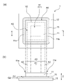
- FIG. 1(a) is a schematic plan view of one embodiment of the bonded structure of the present invention
- FIG. 1(b) is a schematic cross-sectional view taken along line II in FIG. 1(a).
- FIG. 2(a) is an enlarged view schematically showing a panorama image of the central region A1 of the interface between the material to be joined 11 and the joint portion 15 in the cross-sectional view in the thickness direction of the joined structure 1 shown in FIG. 1(a).
- 2(b) is a schematic panorama image of an end region A2 of the interface between the material to be joined 11 and the joint 15 in a cross-sectional view in the thickness direction of the joined structure 1 shown in FIG. 1(a).
- 3 is an enlarged view shown in FIG.
- FIG. 3(a) is an ultrasonic image of the joined structure 1 of Example 1 before the thermal cycle test
- FIG. 3(b) is an ultrasonic image of the joined structure 1 of Example 1 after the thermal cycle test
- FIG. 4(a) is an ultrasonic image of the joined structure 1 of Comparative Example 1 before the thermal cycle test
- FIG. 4(b) is an ultrasonic image of the joined structure 1 of Comparative Example 1 after the thermal cycle test.
- the joint structure 1 includes a first member to be joined 11 (hereinafter also simply referred to as “member to be joined 11”) and a second member to be joined 12 (hereinafter referred to as “member to be joined”). are also simply referred to as “members 12 to be joined”), and a joining portion 15 is formed adjacently between these members 11 and 12 to be joined.
- the members to be joined 11 and 12 in the joined structure 1 are joined through the joining portion 15 , and no other members are interposed between the members to be joined 11 and 12 and the joining portion 15 .
- the joint structure 1 of the embodiment shown in the figure is in a state in which a joint portion 15 and a first joint member 11 are laminated in this order on one surface of a second joint member 12. .
- the material to be bonded 11 shown in FIGS. 1(a) and 1(b) is configured to be smaller in size than the material to be bonded 12, but is not limited to this form, and the materials to be bonded 11 and 12 are identical to each other. It may be a size, and the member 11 to be joined may be configured to be larger than the member 12 to be joined. Furthermore, although the members to be joined 11 and 12 and the joining portion 15 shown in the same figure are all flat, they may be curved if necessary.
- 1(a) and 1(b) is formed such that its peripheral edge extends outward from the peripheral edge of the member to be joined 11, but is not limited to this form. and the peripheral edge of the workpiece 11 may be aligned with each other.
- each of the members to be joined 11 and 12 is independently preferably a conductor.
- the metal forming the surfaces of the members 11 and 12 to be joined at least one of gold, silver, copper, nickel and titanium is preferably independently selected from the viewpoint of improving conductivity.
- Examples of the materials to be joined 11 and 12 containing such metals include, for example, spacers and heat sinks made of the above metals, semiconductor elements, substrates having at least one of the above metals on their surfaces, and the like. be done.
- As the substrate for example, an insulating substrate or the like having a metal layer such as copper on the surface of a ceramic or aluminum nitride plate can be used.
- the semiconductor element contains at least one element among elements such as Si, Ga, Ge, C, N, and As.
- the metal present on the surfaces of the members 11 and 12 to be joined may be a single metal or an alloy of two or more metals.
- the material to be bonded 11 is preferably a spacer, a heat sink, or a semiconductor element.
- the material to be joined 12 is preferably a substrate.
- the joint portion 15 is a structure containing copper as a main component, and is adjacent between the members to be joined 11 and 12, preferably across the entire plane view.
- the joint portion 15 preferably contains 50% by mass or more, more preferably 60% by mass or more of copper.
- the copper content in the junction can be measured by analyzing a cross section in the thickness direction of the junction structure 1 by energy dispersive X-ray spectroscopy (EDX).
- EDX energy dispersive X-ray spectroscopy
- Such a joint portion 15 can be formed as a sintered body of metal particles by firing a composition containing metal particles containing copper together with both materials to be joined, as shown in a manufacturing method to be described later. can.
- the joint 15, which is a sintered body containing such particles may have a large number of pores in its structure.
- One of the characteristics of the bonded structure of the present invention is that when viewed in cross section in the thickness direction, the bonding ratio between the material to be bonded and the bonding portion is different between the central region and the end regions of the bonded structure. I'm trying.
- the virtual region V1 represented by the plan view shape of the similar shape is defined as the central region A1 of the joint structure 1 do.
- the joint ratio at the interface between at least one of the members to be joined 11 and 12 located in the central region A1 and the joint portion 15 is calculated as follows: 1 joining ratio Rc (hereinafter also simply referred to as “joining ratio Rc”).
- the maximum area A0 is the maximum area of the part where both the materials to be joined 11 and 12 and the joint portion 15 all exist when the joined structure 1 is viewed along the thickness direction Z. As shown in FIG. Therefore, taking the joint structure 1 shown in FIGS. 1(a) and 1(b) as an example, the maximum area A0 coincides with the arrangement area of the material 11 to be joined in plan view.
- the joint ratio at the interface between at least one of the members to be joined 11, 12 located in the end region A2 and the joint portion 15 is referred to as a second joining ratio Rs (hereinafter also simply referred to as “joining ratio Rs”).
- the interface targeted for the bonding ratio Rs is the same interface as the interface targeted for the bonding ratio Rc.
- the ratio (Rs/Rc) of the joining ratio Rs to the joining ratio Rc is preferably 0.6 or more, more preferably 0.7 or more. Also, Rs/Rc is preferably 0.9 or less, more preferably 0.8 or less. That is, in the joint structure 1, the joint ratio of the central region A1 is higher than the joint ratio of the end regions A2 at the interface between at least one of the materials to be joined and the joint portion.
- the present inventors speculate as follows about the reason why the bonded structure can exhibit high bonding reliability when Rs/Rc is within the range described above.
- reference numerals shown in FIG. 1 will be used as an example.
- the joint structure 1 in which the joint 15 is formed between the two members to be joined 11 and 12 typically uses a conductive composition having fluidity as a material for forming the joint 15. It is produced by sintering an object placed between two members 11 and 12 to be joined while applying pressure and increasing the rate of temperature rise.
- the composition since the composition remains fluid at the initial stage of firing, the composition is extruded so as to be positioned outside the peripheral edges of the members 11 and 12 to be joined by pressurization, and the members to be joined 11 and 12 moves so that the density of the composition increases in the central region A1 in plan view.
- the composition was efficiently sintered while the central region A1 in plan view had a relatively dense structure, and sufficient adhesion to the members 11 and 12 to be joined was exhibited.
- a joint portion 15 is formed between the members to be joined 11 and 12 over the entire area of the members to be joined 11 and 12 in plan view.
- the bonding ratio Rc is preferably 0.3 or more, more preferably 0.4 or more, and still more preferably 0.5 or more, and the higher the bonding ratio, the better, from the viewpoint of developing sufficient bonding strength with the material to be bonded.
- the bonding ratio Rs is preferably 0.35 or more and 0.6 or less, more preferably 0.35 or more and 0.55 or less, and still more preferably 0.35 or more and 0.5 or less. Since the elastic modulus of the end region A2 of the joined body becomes moderately low due to the joining ratio Rs being such a ratio, it is possible to prevent stress concentration in the end region A2 and the occurrence of cracks. be able to.
- the ratio Rs/Rc, the first bonding ratio Rc, and the second bonding ratio Rs described above define the relationship between at least one of the materials 11 and 12 to be bonded and the bonding portion 15 at least one of the interfaces. It is preferable that at least the interface G1 between the material to be bonded 11 and the bonding portion 15 satisfies the ratio and each bonding ratio. More preferably, it satisfies the above preferred range.
- Such a joint structure 1 is produced by subjecting a conductive composition containing metal particles containing copper together with both the members to be joined 11 and 12 to a predetermined pressure, as shown in the manufacturing method described later, for example. can be obtained by firing at a heating rate of
- the first joining ratio Rc and the second joining ratio Rs can be measured by the following method.
- the joint structure 1 to be measured is embedded in a resin, and then a maximum area A0, a central area A1, and an end area A2 are defined in the plan view of the joint structure 1 by optical microscope observation.
- the resin-embedded joined structure is cut in the thickness direction, the cut surface is polished, and the polished surface is processed by ion milling, for example, as shown in FIG. Prepare an observation surface.
- the position of the interface G1 or the interface G2 between the workpiece to be bonded and the bonding portion to be measured is visually observed using an electron microscope at an arbitrary position within the central region A1 on the observation surface described above. Identify.
- a panoramic image is obtained by photographing and arranging a plurality of images with a magnification that makes the object clear so that the total length Lt of the measurement field is about 30 ⁇ m, for example.
- one of the interfaces G1 and G2 between the workpieces 11 and 12 and the joint 15 is measured, and the total length La along the plane direction X of the part where the interface is unclear is calculated. This is taken as the joining length L1 of the central region A1.
- the joint length L1 is obtained by subtracting the total length of the parts where the interfaces G1 and G2 between the workpieces 11 and 12 to be measured and the joint 15 are clear from the total length Lt of the measurement field.
- FIG. 2A shows a schematic diagram of a panoramic image in the central area A1, taking the interface G1 between the first workpiece 11 and the joint 15 as an example.
- the schematic diagram also shows the total length Lt, the length La, and the joint length L1.
- the ratio (L1/Lt) of the joint length L1 in the central area to the total length Lt of the measurement visual field is defined as the first joint ratio Rc in the present invention.
- the same interface as the interface subjected to the measurement of the joint ratio Rc is determined by visual observation using an electron microscope.
- the total length Lt of the measurement field is about 30 ⁇ m, for example, in the same manner as described above.
- the total length Lb along the plane direction X of the part where the interface between the workpieces 11 and 12 to be measured and the joint 15 is unclear is measured, and the total length Lb of the part is measured.
- the bonding length L2 may be calculated by subtracting the total length of the parts where the interfaces between the workpieces 11 and 12 and the bonding portion 15 are clear from the total length Lt of the measurement field. good.
- the bonding length L2 can be calculated by visually observing the electron microscope image described above and the binarized image described later, or by using software as necessary.
- FIG. 2B shows a schematic diagram of a panoramic image of the end area A2, taking the interface G1 between the first workpiece 11 and the joint 15 as an example.
- the schematic diagram also shows the total length Lt, the length Lb, and the joint length L2. Then, the ratio (L2/Lt) of the joining length L2 of the end area A2 to the total length Lt of the measurement field is defined as the joining ratio Rs in the present invention.
- the interface G1 between the material to be bonded 11 and the bonding portion 15 is clear is determined by binarizing the interface G1 between the material to be bonded 11 to be measured and the bonding portion 15 in the electron microscopic image.
- the interface G1 between the material to be joined 11 and the joint portion 15 is clear if a boundary between a region represented by the same color and a region represented by a different color is observed when the image is viewed along the thickness direction. and On the other hand, if the boundary is not observed, it is assumed that the interface G1 between the workpiece 11 and the joint 15 is unclear.
- the interface G2 between the material to be joined 12 and the joint 15 can also be observed in the same manner as described above to determine whether the interface G2 is clear or unclear.
- the method of measuring the bonding ratios Rc and Rs has been described with a cross-sectional view of the bonded structure 1 in the thickness direction.
- the portion 15 is continuously joined over the entire area of the maximum area A0 in plan view. Therefore, for the joint structure 1, a virtual circle centered on the centroid of the maximum area A0 in a plan view and virtual radial lines that pass through the center of the virtual circle and cut the virtual circle every 30° are considered.
- both the bonding ratios Rc and Rs measured by observing cross sections of the bonded structure in plan view cut in the thickness direction at intervals of 30° along the imaginary radial line are within the above ranges.
- This manufacturing method includes a coating step of applying a bonding composition containing copper on the surface of one of the materials to be bonded (for example, the material to be bonded 12) to form a coating film, and drying the coating film to form a dry coating. It is roughly divided into three processes: a drying process for forming a film, and a bonding process in which the other material to be bonded (for example, the material to be bonded 11) is further laminated on the dried coating film and heated while being pressed while being bonded in this state. be done.
- a bonding composition containing copper is applied to the surface of one of the materials to be bonded to form a coating film (application step).
- the bonding composition preferably comprises metal particles containing copper and a liquid medium. Details of the bonding composition will be described later.
- the method of applying the bonding composition it is preferable to adopt a method that allows the formed coating film to have a uniform thickness and can be applied to the entire surface to be coated.
- coating methods include screen printing, dispense printing, gravure printing, and offset printing.
- the bonding composition is preferably in the form of paste or ink containing a liquid medium.
- the thickness of the coating film to be formed is preferably set to 1 ⁇ m or more and 250 ⁇ m or less, more preferably 5 ⁇ m or more and 150 ⁇ m or less, immediately after coating, from the viewpoint of forming a bonded structure stably having high bonding strength. preferable.
- the formed coating film is dried to obtain a dry coating film (drying process).
- a dry coating film in which the amount of the liquid medium in the coating film is reduced.
- a dry coating film is one in which the ratio of the liquid medium to the total weight of the film is 9% by weight or less. Since the content of each constituent material other than the liquid medium is substantially the same in the coating film and the dry coating film obtained by drying the coating film, the ratio of the liquid medium in the dry coating film is, for example, before and after drying. It can be calculated by measuring the mass change of the coating film.
- a method of volatilizing the liquid medium by utilizing the volatility of the liquid medium can be adopted.
- the proportion of the liquid medium in the dry coating film after the liquid medium has been removed is preferably 9 parts by mass or less, and preferably 7 parts by mass or less, as described above, with respect to the total mass of the coating film of 100 parts by mass. is more preferably 5 parts by mass or less.
- This step can be changed as appropriate depending on the composition of the bonding composition to be used, but it is preferable to perform this step at 40° C. or more and 150° C. or less under atmospheric pressure for 1 minute or more and 60 minutes or less. This is preferable in that deterioration of properties of the article and the materials to be joined together with the articles to be dried hardly occurs, and the bonding strength between the materials to be joined can be increased while maintaining the desired physical properties of the materials to be joined.
- the other member to be joined is laminated on the dry coating film and joined (joining step).
- the dry coating film is obtained through the above-described steps, the other member to be joined is laminated on the dry coating film, and the first member to be joined and the second member to be joined are joined together.
- a laminate is obtained in which the dried coating film is interposed therebetween.
- This laminate is, for example, formed by laminating a coating film and the first member to be joined in this order on one surface of the second member to be joined.
- the laminated body is heated at a predetermined heating rate while being pressurized to sinter the metal powder contained in the dried coating film, thereby forming a joining portion for joining two members to be joined together.
- the atmosphere during sintering is preferably a reducing gas atmosphere such as hydrogen or formic acid, or an inert gas atmosphere such as nitrogen or argon.
- the sintering temperature is preferably 150° C. or higher and 350° C. or lower, more preferably 200° C. or higher and 350° C. or lower, and still more preferably 230° C. or higher and 300° C. or lower.
- the temperature increase rate during sintering is preferably 120°C/min or more and 2000°C/min or less, more preferably 240°C/min or more and 1500°C/min in the process from 40°C to reaching the sintering temperature described above. Below, more preferably 360° C./min or more and 1000° C./min or less.
- This heating rate is faster than the heating rate employed in the manufacture of conventional bonded structures. By carrying out at such a speed, it is possible to manufacture a bonded structure that satisfies the aforementioned Rs/Rc relationship in a short period of time.
- the pressure applied during sintering is preferably more than 6 MPa and 40 MPa or less, more preferably 8 MPa or more and 30 MPa or less, still more preferably 10 MPa or more and 20 MPa or less, from the start of heating to the end of sintering.
- the sintering time is preferably 0.5 minutes or more and 120 minutes or less, more preferably 1 minute or more and 60 minutes or less, and preferably 1 minute or more and 30 minutes or less, provided that the sintering temperature is within the above range. .
- the joint structure 1 in which the joint 15 as a sintered body of metal particles containing copper constituting the joint composition is formed between the two members 11 and 12 to be joined is obtained.
- the above-described Rs/Rc relationship is set between the first workpiece 11 and the bonding portion 15 and between the second workpiece 12 and the bonding portion 15 respectively. It is possible to suitably obtain a joined structure 1 which is filled.
- the bonding portion 15 contains copper, and when the bonding composition contains a solid reducing agent to be described later, the following structure (1) is formed in the bonding layer.
- R 3 to R 5 are each independently a hydrogen atom, a hydroxyl group, a hydrocarbon group having 1 to 10 carbon atoms, or a hydrocarbon group having 1 to 10 carbon atoms and having a hydroxyl group. represents For the details of R 3 to R 5 , the explanations of chemical formulas (2) and (3) below are appropriately applied. Moreover, * represents a binding site with copper.
- Whether or not the structure (1) is formed in the bonding layer can be confirmed by subjecting the cross section of the bonding portion to mass spectrometry or the like using TOF-SIMS.
- TOF-SIMS mass spectrometry
- BIS-TRIS is used as a reducing agent
- a fragment of m/z 152 due to “CN(Cu) 2 ” is observed in the mass spectrum on the positive electrode side in TOF-SIMS.
- the bonding composition contains metal powder composed of metal particles containing copper, and preferably further contains a reducing agent and a liquid medium.
- the metal powder used in the present invention preferably consists of aggregates of metal particles containing copper.
- the metal powder may further contain at least one metal selected from gold, silver, palladium, aluminum, nickel and tin, if necessary.
- the shape of the metal particles that make up the metal powder used in the present invention is, for example, spherical, flake-like, dendrite-like (dendritic), rod-like, and the like. These can be used singly or in combination.
- the particle size is preferably 0.03 ⁇ m or more in terms of volume cumulative particle size D SEM50 at a cumulative volume of 50% measured by image analysis of scanning electron microscope observation, It is more preferably 0.05 ⁇ m or more. Moreover, it is preferably 20 ⁇ m or less, more preferably 10 ⁇ m or less. With such a particle size, a coating film having a thin and uniform thickness can be formed with high productivity, and the bonding strength between the materials to be bonded can be further increased.
- the volume cumulative particle size D50 at a cumulative volume of 50 % by volume measured by a laser diffraction scattering particle size distribution measurement method is preferably 0.3 ⁇ m or more. It is more preferably 5 ⁇ m or more, and even more preferably 0.7 ⁇ m or more.
- the particle size of the flake-shaped copper particles is preferably 100 ⁇ m or less, more preferably 70 ⁇ m or less, and even more preferably 50 ⁇ m or less, in terms of D50 .
- the term “flake” refers to a shape having a pair of plate surfaces forming the main surfaces of the particles and a side surface orthogonal to these plate surfaces. can be a face.
- the reducing agent contained in the bonding composition is preferably solid at 1 atm and room temperature (25°C). Such a reducing agent is used to promote sintering of the metal particles by firing the composition, thereby developing high bonding strength.
- the reducing agent is advantageously of a chemical structure having at least one amino group and multiple hydroxyl groups.
- Solid at room temperature (25°C) means that the melting point of the reducing agent is greater than 25°C.
- the solid reducing agent is also referred to as "solid reducing agent”.
- the melting point of the solid reducing agent is preferably below the sintering temperature of the metal powder.
- the boiling point of the solid reducing agent is preferably higher than the boiling point of the liquid medium to be described later.
- an aminoalcohol compound represented by the following chemical formula (2) or (3) From the viewpoint of efficiently developing high joint strength when pressure bonding is performed, and from the viewpoint of developing high conductivity reliability after pressure bonding when a conductor is used as the material to be bonded, solid reduction As the agent, it is preferable to use an aminoalcohol compound represented by the following chemical formula (2) or (3).
- R 1 to R 6 each independently represent a hydrogen atom, a hydroxyl group, a hydrocarbon group having 1 to 10 carbon atoms, or a hydroxyl group having 1 to 10 carbon atoms. represents a hydrocarbon group.
- R 7 represents a hydrocarbon group having 1 to 10 carbon atoms or a hydrocarbon group having 1 to 10 carbon atoms and having a hydroxyl group.
- Hydrocarbon groups include saturated or unsaturated aliphatic groups. The aliphatic group may be linear or branched.
- aminoalcohol compound represented by the chemical formula (2) or (3) include bis(2-hydroxyethyl)iminotris(hydroxymethyl)methane (BIS-TRIS, melting point: 104°C, boiling point: over 300°C, corresponding to chemical formula (2)), 2-amino-2-(hydroxymethyl)-1,3-propanediol (TRIS, melting point: 169-173°C, boiling point: over 300°C, corresponding to chemical formula (2)), 1 , 3-bis(tris(hydroxymethyl)methylamino)propane (BIS-TRIS propane, melting point: 164-165°C, boiling point: over 300°C, corresponding to chemical formula (3)).
- bis(2-hydroxyethyl)iminotris(hydroxymethyl)methane as the solid reducing agent from the viewpoint of obtaining a bonded body that exhibits high bonding strength while enhancing the sinterability of metal particles.
- the proportion of the solid reducing agent in the bonding composition is preferably 0.1 parts by mass or more with respect to 100 parts by mass of the metal powder, from the viewpoint of enhancing the sinterability of the metal particles. Preferably, it is more preferably 1 part by mass or more.
- it is realistic to make it 10 parts by mass or less, and 8 parts by mass or less. It is preferable to set it as, and it is more preferable to set it as 5 mass parts or less.
- the bonding composition preferably further contains a liquid medium.
- the liquid medium is preferably a non-aqueous solvent from the viewpoint of improving the coating properties of the bonding composition, the solubility of the solid reducing agent, and the efficiency of forming a dry coating film due to the appropriate volatility of the liquid medium.
- monohydric or polyhydric alcohols more preferably polyhydric alcohols.
- polyhydric alcohols examples include propylene glycol, ethylene glycol, hexylene glycol, diethylene glycol, 1,3-butanediol, 1,4-butanediol, dipropylene glycol, tripropylene glycol, glycerin, polyethylene glycol 200 and polyethylene glycol 300. etc.
- a liquid medium can be used individually by 1 type or in combination of 2 or more types.
- the liquid medium is preferably 10 parts by mass or more and 40 parts by mass or less, more preferably 10 parts by mass or more and 35 parts by mass or less with respect to 100 parts by mass of the metal powder.
- the bonding composition may contain other components such as a binder component, a surface tension modifier, an antifoaming agent, and a viscosity modifier as long as the effects of the present invention are exhibited.
- the ratio of the other components is preferably 0.1 parts by mass or more and 10 parts by mass or less with respect to 100 parts by mass of the metal powder.
- a bonded body having such a bonding portion is suitably used in an environment exposed to high temperatures, such as an electronic circuit mounted on a vehicle or an electronic circuit mounted with a power device, by taking advantage of its high bonding strength and thermal conductivity. be done.
- Example 1 (1) Preparation of bonding composition
- copper powder spherical copper powder with a D SEM50 of 0.14 ⁇ m and D50 of 4.9 ⁇ m and an aspect ratio (ratio of the length of the main surface to the thickness of the particle) of 13 A mixture with flaky copper powder was used.
- the content ratio of the spherical copper powder and the flaky copper powder in the mixture of copper powder was 70% by mass of spherical copper powder:30% by mass of flaky copper powder.
- Bis(2-hydroxyethyl)iminotris(hydroxymethyl)methane was used as a reducing agent at a ratio of 2.5 parts to 100 parts of copper powder.
- a liquid medium a mixture of polyethylene glycol 300 (1 part per 100 parts of copper powder) and hexylene glycol (31.6 parts per 100 parts of copper powder) was used.
- a pasty bonding composition was obtained by mixing the above copper powder, reducing agent and liquid medium.
- the viscosity of the bonding composition at a shear rate of 10 s -1 was 34 Pa ⁇ s at 25°C.
- a 4.9 mm square semiconductor element SiC chip, thickness 0.38 mm, CPW5-1200 manufactured by Wolfspeed Co., Ltd., square in plan view
- a pressure of 20 MPa is applied in the thickness direction, and the temperature is raised from 40° C. to 280° C. at a temperature elevation rate of 960° C./min in a nitrogen atmosphere, and then baked at 280° C. for 5 minutes.
- each member to be joined and the joint portion were formed adjacent to each other over the entire plane view.
- Mass spectrometry by TOF-SIMS confirmed that the joint portion, which is a sintered body of the dried coating film, had the chemical structure represented by the structure (1).
- Example 2 A bonded structure having the structure shown in FIGS. 1(a) and 1(b) was obtained in the same manner as in Example 1, except that the pressure applied during sintering was changed to 10 MPa in manufacturing the bonded structure. . It was confirmed by TOF-SIMS mass spectrometry that the chemical structure represented by structure (1) was formed in the junction.
- Example 1 A joined structure was obtained in the same manner as in Example 1, except that the pressure applied during sintering was changed to 6 MPa in the production of the joined structure. It was confirmed by TOF-SIMS mass spectrometry that the chemical structure represented by structure (1) was formed in the junction.
- TCT thermal cycle test
- the obtained image data was binarized using image processing software Image-J, and the black area ratio (conjugation ratio after 10 cycles of TCT; %) in the observed area was calculated. That is, after starting Image-J, Analyze-Set measurement was selected, and Area, Area fraction, and Limit to Threshold were checked. After that, File-Open was selected to open the image data for calculating the bonding rate, and then the range (A) of the SiC chip mounting portion in the image was specified. Next, after selecting Edit-Copy to system and copying the specified range (A), File-New-System clipboard was selected and the image of the specified range (A) was pasted.
- Image-Type-8bit was selected to clarify the junction, and after the image was converted, Image-Adjust-Threshold was selected to adjust the threshold of the image to 110.
- a red range (B) existing within the range (A) of the SiC chip mounting portion in the adjusted image was specified.
- the red area (B) is the SiC chip bonding portion, and the bonding rate is calculated by (B)/(A) ⁇ 100. A higher bonding rate indicates a higher bonding reliability even when excessive temperature changes occur. Table 1 shows the results.
Landscapes
- Engineering & Computer Science (AREA)
- Chemical & Material Sciences (AREA)
- Materials Engineering (AREA)
- Mechanical Engineering (AREA)
- Manufacturing & Machinery (AREA)
- Composite Materials (AREA)
- Nanotechnology (AREA)
- Microelectronics & Electronic Packaging (AREA)
- Computer Hardware Design (AREA)
- Power Engineering (AREA)
- Metallurgy (AREA)
- Organic Chemistry (AREA)
- Inorganic Chemistry (AREA)
- General Physics & Mathematics (AREA)
- Condensed Matter Physics & Semiconductors (AREA)
- Physics & Mathematics (AREA)
- Ceramic Engineering (AREA)
- Powder Metallurgy (AREA)
- Pressure Welding/Diffusion-Bonding (AREA)
- Arc Welding In General (AREA)
Abstract
Description
前記接合部は、銅を主体とする材料からなり、
前記接合構造体の厚み方向断面視において、該接合構造体の中央域における前記被接合材と前記接合部との接合割合Rcに対する、該接合構造体の端部域における前記被接合材と前記接合部との接合割合Rsの比(Rs/Rc)が、0.6以上0.9以下であり、
前記接合割合Rcが0.3以上である、接合構造体を提供するものである。
被接合材11は、スペーサー、放熱板、又は半導体素子のいずれかであることが好ましい。被接合材12は、好ましくは基板である。
このような接合部15は、例えば後述する製造方法にて示すように、銅を含む金属粒子を含む組成物を両被接合材とともに焼成して、金属粒子どうしの焼結体として形成することができる。このような粒子を含んで形成された焼結体である接合部15は、その構造中に多数の空孔を有していてもよい。
なお、最大領域A0は、接合構造体1を厚み方向Zに沿ってみたときに、両被接合材11,12と接合部15とのすべてが存在する部位の最大の領域である。したがって、図1(a)及び(b)に示される接合構造体1を例にとると、最大領域A0は、被接合材11の平面視における配置領域と一致する。
2つの被接合材11,12の間に接合部15が形成された接合構造体1は、典型的には、接合部15の形成材料として流動性を有する導電性の組成物を用い、この組成物を2つの被接合材11,12の間に配した状態で、加圧しながら昇温速度を早くした状態で焼成して作製される。このとき、組成物は焼成初期では流動性が残存しているので、加圧によって、被接合材11,12の周縁外方に位置するように組成物が押し出されたり、被接合材11,12の平面視中央域A1において組成物の密度が高まるように移動したりする。この状態で焼結されることによって、平面視中央域A1では比較的密な構造となりつつ、組成物が効率的に焼結して、被接合材11,12との密着性が十分に発現した接合部15が各被接合材11,12の間に該被接合材11,12の平面視全域に形成される。特に、Rs/Rcが上述した特定の範囲にあると、接合構造体1全体としての接合強度が維持されると共に、接合構造体1の端部域A2における応力集中が緩和されることとなるため、温度変化環境においても接合部の高い接合機能が維持され、高い接合信頼性を維持することができる。
これに対し、加圧が不十分である条件や、昇温速度が適切でない条件で接合部15が形成される場合には、接合構造体1の平面視中央域A1に位置する接合部15が密な構造となり難く、Rs/Rcが1に近い値となる。そうすると、接合部15の端部域A2における応力集中の緩和ができなくなり、接合信頼性を維持することが困難となる。
このような接合構造体1は、例えば後述する製造方法にて示すように、銅を含む金属粒子を含む導電性組成物を両被接合材11,12とともに所定の圧力を付与した状態で、所定の昇温速度で焼成することによって得ることができる。
まず測定対象の接合構造体1を樹脂包埋したあと、光学顕微鏡観察によって、接合構造体1の平面視において、最大領域A0、中央域A1及び端部域A2をそれぞれ画定する。その後、最大領域A0の平面視での図心(図1(a)中、第1の被接合材11の平面視における図心に相当する)を通過する位置で、樹脂包埋した接合構造体を厚み方向に切断し、当該切断面を研磨して、更にイオンミリングにより研磨面を加工した後、例えば図1(b)で示されるように、図心を通過する厚み方向断面視に相当する観察面を作製する。
図2(a)には、第1の被接合材11と接合部15との界面G1を例にとり、中央域A1におけるパノラマ像の模式図が示されている。同模式図では、全長Lt、長さLa及び接合長さL1を併せて示している。
そして、測定視野の全長Ltに対する中央域の接合長さL1の比(L1/Lt)を、本発明における第1接合割合Rcとする。
図2(b)には、第1の被接合材11と接合部15との界面G1を例にとり、端部域A2のパノラマ像の模式図が示されている。同模式図では、全長Lt、長さLb及び接合長さL2を併せて示している。
そして、測定視野の全長Ltに対する端部域A2の接合長さL2の比(L2/Lt)を、本発明における接合割合Rsとする。
被接合材12と接合部15との界面G2についても、上述の方法と同様に観察して、界面G2が明瞭又は不明瞭と判定することができる。
液媒体が除去された後の乾燥塗膜における該液媒体の割合は、塗膜の全質量100質量部に対して、上述のとおり9質量部以下であることが好ましく、7質量部以下であることが更に好ましく、5質量部以下であることが更に好ましい。
本工程は、用いる接合用組成物の組成に応じて適宜変更可能であるが、大気雰囲気下で、40℃以上150℃以下、大気圧、1分以上60分以下で行うことが、接合用組成物及びこれとともに乾燥に供される被接合材の変質が生じ難く、被接合材の所望の物性を維持しつつ、被接合材どうしの接合強度を高められる点で好ましい。
そして、積層体を加圧しながら所定の昇温速度で加熱して、乾燥塗膜に含まれる金属粉を焼結させることで、2つの被接合材どうしを接合する接合部を形成する。
焼結温度は、好ましくは150℃以上350℃以下、より好ましくは200℃以上350℃以下、更に好ましくは230℃以上300℃以下である。
焼結時間は、焼結温度が上述の範囲にある状態を条件として、好ましくは0.5分以上120分以下、より好ましくは1分以上60分以下、好ましくは1分以上30分以下である。


(1)接合用組成物の調製
銅粉として、DSEM50が0.14μmの球状銅粉と、D50が4.9μmでアスペクト比(粒子の厚みに対する主面の長さの比)が13のフレーク状銅粉との混合物を用いた。銅粉の混合物中に占める球状銅粉とフレーク状銅粉の含有割合は、球状銅粉70質量%:フレーク状銅粉30質量%とした。
還元剤としてビス(2-ヒドロキシエチル)イミノトリス(ヒドロキシメチル)メタンを、銅粉100部に対して2.5部の割合で用いた。
液媒体として、ポリエチレングリコール300(銅粉100部に対して1部)とヘキシレングリコール(銅粉100部に対して31.6部)との混合物を用いた。
上述した銅粉、還元剤及び液媒体を混合してペースト状の接合用組成物を得た。
せん断速度10s-1における接合用組成物の粘度は25℃において34Pa・sであった。
第2の被接合材として、20mm四方の平面視正方形の銅板(厚み1mm)の中央に、スクリーン印刷によって接合用組成物を塗布して塗膜を形成した。塗膜は、厚み100μmのメタルマスクを用いて、銅板の中央部を含む領域に、6mm四方の正方形に形成した。この塗膜を熱風乾燥機中、110℃、10分で乾燥させて液媒体を一部除去し、室温下に放置して、乾燥塗膜を得た。また、乾燥塗膜中の液媒体の含有量を確認した結果、5質量%以下であった。
接合構造体の製造において、焼結時の圧力付与を10MPaに変更した以外は、実施例1と同様の方法で、図1(a)及び(b)に示す構造を有する接合構造体を得た。接合部は、前記の構造(1)で表される化学構造が形成されていることを、TOF-SIMSによる質量分析によって確認した。
接合構造体の製造において、焼結時の圧力付与を6MPaに変更した以外は、実施例1と同様の方法で接合構造体を得た。接合部は、前記の構造(1)で表される化学構造が形成されていることを、TOF-SIMSによる質量分析によって確認した。
実施例及び比較例の接合構造体について、株式会社システムインフロンティア製のソフトウェアMeasurementAdviserを用いて、被接合材と接合部との界面における各接合割合Rc,Rs並びにこれらの比Rs/Rcを、上述した方法でそれぞれ測定及び算出した。その結果を測定視野の全長Ltとともに以下の表1に示す。
なお説明の便宜上、以下の表中では、SiCチップ(第1の被接合材11)と接合部15との間の接合割合のみを示している。
接合構造体に対して、冷熱サイクル試験(TCT)を10サイクル行い、そのときの焼結体からの剥離の状態を超音波探傷装置(日立パワーソリューションズ社製、型番:FineSAT III)を用い、75MHzのプローブにて反射法によって、銅板の裏面側から観察した。TCTでは、(1)-40℃・15分間、(2)+125℃・15分間、を1サイクルとした。
接合層の剥離状態を観察する際、ゲインの値を25~35dBの値にした後、Sゲートのピーク位置が銅板の表面となるようSゲートのディレイと幅を調節した。接合層の観察範囲を指定するためFゲートのディレイを調整し、幅を1.5波長分のピーク幅に設定した。観察ピークの振幅が最大となるようプローブのZ軸座標を調整し、観察を行った。観察像のコントラストはオート機能を用いて調節した。
上述の装置では、接合状態が良好であるものは色が濃く(黒色に)観察され、クラックや剥離が発生し接合状態が悪い領域は色が薄く(白色に)観察される。このうち、実施例1及び比較例1のTCT前後の画像データを図3及び図4に示す。
また、得られた画像データを画像処理ソフトウェアImage-Jを用いて二値化し、観察した面積中における黒色の面積割合(TCT10サイクル後の接合率;%)を算出した。すなわち、Image-Jを起動した後、Analyze-Set measurementを選択し、Area、Area fraction、Limit to Thresholdにチェックを入れた。その後、File-Openを選択し、接合率を算出する画像データを開いた後に、画像中のSiCチップ搭載部の範囲(A)を指定した。次いで、Edit-Copy to systemを選択し、指定した範囲(A)をコピーした後、File-New-System clipboardを選択して指定した範囲(A)の画像を貼り付けた。その後、接合部を明確にするために、Image-Type-8bitを選択し、画像を変換した後、Image-Adjust-Thresholdを選択して画像の閾値を110に調整した。そして、調整後の画像におけるSiCチップ搭載部の範囲(A)内に存在する赤色範囲(B)を指定した。前記赤色範囲(B)がSiCチップ接合部となり、その接合率は(B)/(A)×100で算出される。接合率が高いほど、過度な温度変化が発生した場合でも接合信頼性が高いことを示す。結果を表1に示す。

Claims (3)
- 2つの被接合材と、これらの被接合材間に隣接して形成された接合部とが接合されてなる接合構造体であって、
前記接合部は、銅を主体とする材料からなり、
前記接合構造体の厚み方向断面視において、該接合構造体の中央域における前記被接合材と前記接合部との接合割合Rcに対する、該接合構造体の端部域における前記被接合材と前記接合部との接合割合Rsの比(Rs/Rc)が、0.6以上0.9以下であり、
前記接合割合Rcが0.3以上である、接合構造体。 - 前記被接合材の少なくとも一方は、その表面に金、銀、銅、ニッケル及びチタンの少なくとも一種の金属を有する、請求項1に記載の接合構造体。
- 前記接合部に以下の式(1)で示される構造が形成されている、請求項1又は2に記載の接合構造体。

*は、銅との結合部位を表す。)
Priority Applications (5)
| Application Number | Priority Date | Filing Date | Title |
|---|---|---|---|
| KR1020237028510A KR20230162592A (ko) | 2021-03-30 | 2022-03-28 | 접합 구조체 |
| EP22780688.2A EP4316694A1 (en) | 2021-03-30 | 2022-03-28 | Joint structure |
| US18/279,012 US20240149340A1 (en) | 2021-03-30 | 2022-03-28 | Joint structure |
| CN202280019470.5A CN116963856A (zh) | 2021-03-30 | 2022-03-28 | 接合结构体 |
| JP2023511226A JPWO2022210477A1 (ja) | 2021-03-30 | 2022-03-28 |
Applications Claiming Priority (2)
| Application Number | Priority Date | Filing Date | Title |
|---|---|---|---|
| JP2021058724 | 2021-03-30 | ||
| JP2021-058724 | 2021-03-30 |
Publications (1)
| Publication Number | Publication Date |
|---|---|
| WO2022210477A1 true WO2022210477A1 (ja) | 2022-10-06 |
Family
ID=83459045
Family Applications (1)
| Application Number | Title | Priority Date | Filing Date |
|---|---|---|---|
| PCT/JP2022/014835 WO2022210477A1 (ja) | 2021-03-30 | 2022-03-28 | 接合構造体 |
Country Status (7)
| Country | Link |
|---|---|
| US (1) | US20240149340A1 (ja) |
| EP (1) | EP4316694A1 (ja) |
| JP (1) | JPWO2022210477A1 (ja) |
| KR (1) | KR20230162592A (ja) |
| CN (1) | CN116963856A (ja) |
| TW (1) | TW202242910A (ja) |
| WO (1) | WO2022210477A1 (ja) |
Cited By (1)
| Publication number | Priority date | Publication date | Assignee | Title |
|---|---|---|---|---|
| WO2023190573A1 (ja) * | 2022-03-30 | 2023-10-05 | 三井金属鉱業株式会社 | 接合体の製造方法及び被接合体の接合方法 |
Citations (4)
| Publication number | Priority date | Publication date | Assignee | Title |
|---|---|---|---|---|
| WO2008032386A1 (fr) * | 2006-09-14 | 2008-03-20 | Sumitomo Bakelite Co., Ltd. | Structure de jonction, procédé de jonction, plaquette de câblage et son procédé de production |
| JP2014029897A (ja) * | 2012-07-31 | 2014-02-13 | Hitachi Ltd | 導電性接合体およびそれを用いた半導体装置 |
| WO2020032161A1 (ja) | 2018-08-08 | 2020-02-13 | 三井金属鉱業株式会社 | 接合用組成物、並びに導電体の接合構造及びその製造方法 |
| JP2020038896A (ja) * | 2018-09-04 | 2020-03-12 | 古河電気工業株式会社 | 接合構造体及び接合構造体の製造方法 |
-
2022
- 2022-03-28 WO PCT/JP2022/014835 patent/WO2022210477A1/ja active Application Filing
- 2022-03-28 US US18/279,012 patent/US20240149340A1/en active Pending
- 2022-03-28 KR KR1020237028510A patent/KR20230162592A/ko unknown
- 2022-03-28 CN CN202280019470.5A patent/CN116963856A/zh active Pending
- 2022-03-28 JP JP2023511226A patent/JPWO2022210477A1/ja active Pending
- 2022-03-28 EP EP22780688.2A patent/EP4316694A1/en active Pending
- 2022-03-30 TW TW111112164A patent/TW202242910A/zh unknown
Patent Citations (4)
| Publication number | Priority date | Publication date | Assignee | Title |
|---|---|---|---|---|
| WO2008032386A1 (fr) * | 2006-09-14 | 2008-03-20 | Sumitomo Bakelite Co., Ltd. | Structure de jonction, procédé de jonction, plaquette de câblage et son procédé de production |
| JP2014029897A (ja) * | 2012-07-31 | 2014-02-13 | Hitachi Ltd | 導電性接合体およびそれを用いた半導体装置 |
| WO2020032161A1 (ja) | 2018-08-08 | 2020-02-13 | 三井金属鉱業株式会社 | 接合用組成物、並びに導電体の接合構造及びその製造方法 |
| JP2020038896A (ja) * | 2018-09-04 | 2020-03-12 | 古河電気工業株式会社 | 接合構造体及び接合構造体の製造方法 |
Cited By (1)
| Publication number | Priority date | Publication date | Assignee | Title |
|---|---|---|---|---|
| WO2023190573A1 (ja) * | 2022-03-30 | 2023-10-05 | 三井金属鉱業株式会社 | 接合体の製造方法及び被接合体の接合方法 |
Also Published As
| Publication number | Publication date |
|---|---|
| JPWO2022210477A1 (ja) | 2022-10-06 |
| EP4316694A1 (en) | 2024-02-07 |
| KR20230162592A (ko) | 2023-11-28 |
| TW202242910A (zh) | 2022-11-01 |
| CN116963856A (zh) | 2023-10-27 |
| US20240149340A1 (en) | 2024-05-09 |
Similar Documents
| Publication | Publication Date | Title |
|---|---|---|
| JP7190529B2 (ja) | 接合用組成物、並びに導電体の接合構造及びその製造方法 | |
| US20220157765A1 (en) | Bonding material and bonded structure | |
| WO2022210477A1 (ja) | 接合構造体 | |
| JP7155654B2 (ja) | 接合体の製造方法 | |
| JP7317397B2 (ja) | 酸化銅ペースト及び電子部品の製造方法 | |
| JP7150144B2 (ja) | 加圧接合用組成物、並びに導電体の接合構造及びその製造方法 | |
| JP6565527B2 (ja) | Ag下地層付パワーモジュール用基板及びパワーモジュール | |
| KR20170063544A (ko) | Ag 하지층이 형성된 파워 모듈용 기판 및 파워 모듈 | |
| JP6606514B2 (ja) | 金属粒子及び導電性材料の粒子を用いた導電性接合材料並びに導電性接合構造 | |
| EP4122624A1 (en) | Bonding sheet and bonded structure | |
| WO2020202970A1 (ja) | 接合体及びその製造方法 | |
| TW202231398A (zh) | 氧化銅糊料及電子零件之製造方法 | |
| JP2024021288A (ja) | 金属製部材の接合方法及び銀焼結体 | |
| CN114845827A (zh) | 银膏及其制造方法以及接合体的制造方法 |
Legal Events
| Date | Code | Title | Description |
|---|---|---|---|
| 121 | Ep: the epo has been informed by wipo that ep was designated in this application |
Ref document number: 22780688 Country of ref document: EP Kind code of ref document: A1 |
|
| ENP | Entry into the national phase |
Ref document number: 2023511226 Country of ref document: JP Kind code of ref document: A |
|
| WWE | Wipo information: entry into national phase |
Ref document number: 18279012 Country of ref document: US |
|
| WWE | Wipo information: entry into national phase |
Ref document number: 202280019470.5 Country of ref document: CN |
|
| WWE | Wipo information: entry into national phase |
Ref document number: 2022780688 Country of ref document: EP |
|
| NENP | Non-entry into the national phase |
Ref country code: DE |
|
| ENP | Entry into the national phase |
Ref document number: 2022780688 Country of ref document: EP Effective date: 20231030 |