WO2022209714A1 - Rfidモジュールを備えた容器 - Google Patents
Rfidモジュールを備えた容器 Download PDFInfo
- Publication number
- WO2022209714A1 WO2022209714A1 PCT/JP2022/010700 JP2022010700W WO2022209714A1 WO 2022209714 A1 WO2022209714 A1 WO 2022209714A1 JP 2022010700 W JP2022010700 W JP 2022010700W WO 2022209714 A1 WO2022209714 A1 WO 2022209714A1
- Authority
- WO
- WIPO (PCT)
- Prior art keywords
- container
- rfid module
- metal layer
- slot
- module according
- Prior art date
- Legal status (The legal status is an assumption and is not a legal conclusion. Google has not performed a legal analysis and makes no representation as to the accuracy of the status listed.)
- Ceased
Links
Images






Classifications
-
- B—PERFORMING OPERATIONS; TRANSPORTING
- B65—CONVEYING; PACKING; STORING; HANDLING THIN OR FILAMENTARY MATERIAL
- B65D—CONTAINERS FOR STORAGE OR TRANSPORT OF ARTICLES OR MATERIALS, e.g. BAGS, BARRELS, BOTTLES, BOXES, CANS, CARTONS, CRATES, DRUMS, JARS, TANKS, HOPPERS, FORWARDING CONTAINERS; ACCESSORIES, CLOSURES, OR FITTINGS THEREFOR; PACKAGING ELEMENTS; PACKAGES
- B65D65/00—Wrappers or flexible covers; Packaging materials of special type or form
- B65D65/38—Packaging materials of special type or form
- B65D65/40—Applications of laminates for particular packaging purposes
-
- G—PHYSICS
- G06—COMPUTING OR CALCULATING; COUNTING
- G06K—GRAPHICAL DATA READING; PRESENTATION OF DATA; RECORD CARRIERS; HANDLING RECORD CARRIERS
- G06K19/00—Record carriers for use with machines and with at least a part designed to carry digital markings
- G06K19/06—Record carriers for use with machines and with at least a part designed to carry digital markings characterised by the kind of the digital marking, e.g. shape, nature, code
- G06K19/067—Record carriers with conductive marks, printed circuits or semiconductor circuit elements, e.g. credit or identity cards also with resonating or responding marks without active components
- G06K19/07—Record carriers with conductive marks, printed circuits or semiconductor circuit elements, e.g. credit or identity cards also with resonating or responding marks without active components with integrated circuit chips
- G06K19/077—Constructional details, e.g. mounting of circuits in the carrier
-
- H—ELECTRICITY
- H01—ELECTRIC ELEMENTS
- H01Q—ANTENNAS, i.e. RADIO AERIALS
- H01Q13/00—Waveguide horns or mouths; Slot antennas; Leaky-waveguide antennas; Equivalent structures causing radiation along the transmission path of a guided wave
- H01Q13/10—Resonant slot antennas
-
- H—ELECTRICITY
- H01—ELECTRIC ELEMENTS
- H01Q—ANTENNAS, i.e. RADIO AERIALS
- H01Q19/00—Combinations of primary active antenna elements and units with secondary devices, e.g. with quasi-optical devices, for giving the antenna a desired directional characteristic
- H01Q19/02—Details
Definitions
- the present invention relates to a container equipped with an RFID module, particularly a container equipped with an RFID module using RFID (Radio Frequency Identification) technology for non-contact data communication using an induced electromagnetic field or radio waves.
- RFID Radio Frequency Identification
- RFID tags which are wireless communication devices
- An RFID tag together with RFIC (Radio-Frequency Integrated Circuit)
- RFIC Radio-Frequency Integrated Circuit
- a metal material such as an antenna pattern formed on an insulating substrate such as paper or resin.
- the RFID tag will be affected and will not be able to communicate.
- Patent Document 1 proposes a configuration in which an RFID tag that is compatible with metal formed on a part of the container is provided so as not to impair the design.
- the RFID tag disclosed in Patent Document 1 has an RFIC chip and an antenna pattern, and a metal layer cannot be formed on the container in these areas. Therefore, there is a demand for a container having an RFID module that suppresses a reduction in the degree of design freedom.
- An object of the present invention is to provide a container having an RFID module that suppresses deterioration of design in a container on which a metal layer is formed.
- a container of one embodiment of the present invention is a container provided with an RFID module, which includes a packaging material having a resin base material and a metal layer formed on the base material, and a peripheral edge of the packaging material.
- the RFID module includes an RFIC element, a filter circuit for transmitting a current due to electromagnetic waves having a unique resonance frequency, which is a communication frequency, to the RFIC element, and first and second electrodes connected to the filter circuit.
- the first electrode of the RFID module and the metal layer are electrically connected.
- the second electrode of the RFID module and the metal layer are electrically connected across the slot by the RFID module.
- the present invention it is possible to provide a container having an RFID module that suppresses deterioration in design in a container on which a metal layer is formed.
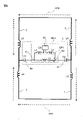
- FIG. 1 is a plan view of a container having an RFID module according to Embodiment 1;
- FIG. 6A is a plan view of a conductor pattern formed on the substrate of the RFID module;
- FIG. 6B is a plan view of the conductor pattern formed on the bottom surface of the substrate; perspective plan view from above Sectional view of arrow VII in FIG.
- FIG. 11 is a plan view of the cut first seal portion of the container in the modified example of the first embodiment; Partial plan view of the container in the modification of Embodiment 1 Partial plan view of the container in the modification of Embodiment 1 Partial plan view of the container in the modification of Embodiment 1 Partial plan view of the container in the modification of Embodiment 1 Partial plan view of the container in the modification of Embodiment 1 Partial plan view of the container in the modification of Embodiment 1 Partial plan view of the container in the modification of Embodiment 1 Partial plan view of the container in the modification of Embodiment 1 Partial plan view of the container in the modification of Embodiment 1
- a container according to one aspect of the present invention is a container provided with an RFID module, the packaging material having a resin base material and a metal layer formed on the base material, and the peripheral edge of the packaging material
- the container includes a container for containing contents inside the seals joined to each other, and a slot formed in the seals.
- the RFID module includes an RFIC element, a filter circuit for transmitting a current due to electromagnetic waves having a unique resonance frequency, which is a communication frequency, to the RFIC element, and first and second electrodes connected to the filter circuit.
- the first electrode of the RFID module and the metal layer are electrically connected.
- the second electrode of the RFID module and the metal layer are electrically connected across the slot by the RFID module.
- the container of this aspect uses the metal layer formed on the base material of the container as an antenna, in the container in which the metal layer is formed, the RFID module can be attached to the container while suppressing the reduction in the degree of freedom of design. can be done.
- the container may have a through hole formed in the sealing portion. Since the container has a through hole, the container can be suspended by passing the support rod through the through hole.
- the through hole may be formed on the extension of the slot in the direction in which the slot extends. Thereby, the through holes and the slots can be formed at the same time, and the processing cost can be reduced.
- the through-hole may be formed outside the container rather than the slot. This can reduce deformation of the container when the support rod is passed through the through hole.
- the through hole may be formed inside the container rather than the slot.
- the metal layer when the metal layer is irradiated with an electromagnetic wave of a communication frequency, a current may flow in the direction of circling the slot. In this way, the metal layer functions as a slot antenna, so communication characteristics of a slot antenna can be obtained.
- the length of the slot may have the physical length of half the wavelength of the electromagnetic wave at the communication frequency. In this case, the maximum communication distance as a slot antenna is often obtained.
- the filter circuit may be an LC parallel resonant circuit. As a result, a current with a frequency that matches the RFIC can be passed through the RFIC.
- the filter circuit has a coil formed on the substrate, and the coil may be covered with a protective layer. Thereby, the dielectric constant of the coil can be fixed, and the influence of the dielectric inside the container can be prevented.
- the coil of the filter circuit may have a figure-of-eight shape. This makes it difficult for the magnetic field of the coil to leak to the outside, and makes it difficult for the inductance value of the coil to change due to external factors.
- the sheet resistance of the metal layer may be 0.5 ⁇ / ⁇ or more. Even with this configuration, since the RFID module has a filter circuit, the eddy current generated in the metal layer can be used to flow to the RFIC.
- the thickness of the metal layer may be 1 nm or more and 1 ⁇ m or less. Even with this configuration, since the RFID module has a filter circuit, the eddy current generated in the metal layer can be used to flow to the RFIC.
- the electrical lengths of the antenna pattern and the conductor pattern are longer than their physical lengths.
- the electrical length is a length that takes into account wavelength shortening due to relative permittivity and parasitic reactance components.
- FIG. 1 is an overall perspective view of a container 1 having an RFID module 5 according to Embodiment 1 of the present invention.
- 2 is a cross-sectional view taken along arrow II in FIG. 1
- FIG. 3 is a cross-sectional view taken along arrow III in FIG.
- the container 1 of Embodiment 1 includes a packaging material 3 , an RFID module 5 attached to the packaging material 3 , and a slot 9 formed in the packaging material 3 .
- one side of the container 1 is defined as an upper side
- a side opposite to the upper side is defined as a lower side
- a side connecting the upper side and the lower side is defined as a lateral side.
- the through holes 11 are arranged on the upper side.
- the container 1 is, for example, a bag-like container formed by joining, for example, thermocompression bonding the peripheral edge portions of two flat packaging materials 3 as shown in FIG.
- the container 1 includes a storage portion 2 for storing contents inside, and a seal portion 4 to which packaging materials 3 on the front and back sides are respectively joined.
- the seal portion 4 has a first seal portion 4 a above the housing portion 2 and second seal portions 4 b laterally and below the housing portion 2 .
- the container 1 can have the first seal portion 4 a cut off from the end of the packaging material 3 . Since the container 1 has the chuck 2a on the upper part of the housing part 2, the container 1 can be opened and closed even after the first seal part 4a is cut off from the container 1. As shown in FIG.
- the packaging material 3 includes a base material 6 , a metal layer 7 laminated on the base material 6 , a printed layer 8 laminated on the metal layer 7 , and a cover layer 10 formed on the printed layer 8 .
- the base material 6 is a resin layer, for example polypropylene.
- the metal layer 7 is made of a film of a conductive material such as aluminum foil or copper foil, and is formed, for example, by attaching a metal sheet. A communication distance can be increased by using a metal having a low resistance value, such as aluminum or copper, as the metal layer 7 .
- the thickness of the metal layer 7 is, for example, greater than 5 ⁇ m and equal to or less than 40 ⁇ m.
- the metal layer 7 is formed on the entire surface of the packaging material 3 except for the slots 9 in FIG. It may be partially formed in the first seal portion 4a.
- the printed layer 8 is a resin layer printed using ink.
- the printing layer 8 is, for example, polyethylene, and characters and figures are printed thereon by inkjet printing, gravure printing, offset printing, or the like. Note that the packaging material 3 may not have the printed layer 8 .
- the cover layer 10 is a layer that protects the metal layer 7 and the printed layer 8 from moisture and dirt.
- the cover layer 10 is a resin layer, such as polypropylene.
- the through hole 11 is a hole for passing the container 1 through, for example, a support rod. As a result, the container 1 can be displayed by hanging it from a rod.
- the through hole 11 is formed in the seal portion 4, for example, on the extension of the slot 9 in the direction in which the slot 9 extends in the first seal portion 4a. As a result, the slot 9 and the through hole 11 can be formed simultaneously using a mold, and the processing cost can be reduced. Note that the container 1 may not have the through holes 11 .
- the slot 9 is a groove formed at least within the area of the metal layer 7 . As shown in FIG. 2, a groove penetrating the packaging material 3 may be used.
- the slots 9 may be formed at the same time when the through holes 11 are formed using a mold, or may be formed by scraping the metal layer 7 with, for example, sandpaper.
- the slot 9 may be formed in the second sealing portion 4b of the packaging material 3.
- the communication distance is maximized.
- the container 1 is irradiated with an electromagnetic wave having a communication frequency, communication is performed in a direction circulating the slot 9 so as to reciprocate from the RFID module 5 positioned at the center of the slot 9 in the longitudinal direction to the ends of the two slots 9 respectively. It resonates with the frequency and current Ir flows (see FIG. 1).
- the width W of the slot 9 is, for example, 1 mm.
- the RFID module 5 is a wireless communication device configured to wirelessly communicate (transmit and receive) using high-frequency signals having a communication frequency (carrier frequency).
- the RFID module 5 is configured, for example, to wirelessly communicate with a high-frequency signal having a frequency for UHF band communication.
- the UHF band is a frequency band from 860 MHz to 960 MHz.
- FIG. 4 is a perspective plan view of the RFID module
- FIG. 5 is a cross-sectional view taken along arrow V in FIG. 6 shows a plan view of the conductor pattern formed on the substrate of the RFID module
- FIG. 6a is a plan view of the conductor pattern formed on the upper surface of the substrate of the RFID module
- FIG. 6b is a plan view of the conductor pattern formed on the lower surface of the substrate.
- 1 is a perspective plan view of a conductor pattern seen from above
- FIG. 7 is a cross-sectional view taken along line VII in FIG. 4.
- FIG. In the drawings, the XYZ coordinate system is intended to facilitate understanding of the invention and is not intended to limit the invention.
- the X-axis direction indicates the longitudinal direction of the RFID module 5
- the Y-axis direction indicates the depth (width) direction
- the Z-axis direction indicates the thickness direction.
- the X, Y and Z directions are orthogonal to each other.
- the printing layer 8 and the cover layer 10 of the packaging material 3 on the back side and the packaging material 3 on the front side are omitted.
- the RFID module 5 is attached across the slot 9 to the upper surface of the packaging material 3 via double-sided tape or adhesive 15 such as synthetic resin.
- the RFID module 5 includes a substrate 21 and an RFIC 23 mounted on the substrate 21.
- the substrate 21 is, for example, a flexible substrate such as polyimide.
- a protective film 25 is formed on the upper surface of the substrate 21 on which the RFIC 23 is mounted.
- the protective film 25 is, for example, an elastomer such as polyurethane or a hot melt agent such as ethylene vinyl acetate (EVA).
- a protective film 27 is also attached to the lower surface of the substrate 21 .
- the protective film 27 is, for example, a coverlay film such as a polyimide film (Kapton tape).
- a third electrode 33, a fourth electrode 35, a conductor pattern L1a of the main portion of the first inductance element L1, and a conductor pattern L2a of the main portion of the second inductance element L2 are formed on the upper surface of the substrate 21.
- FIG. The third electrode 33 is connected to one end of the conductor pattern L1a
- the fourth electrode 35 is connected to one end of the conductor pattern L2a.
- a first electrode 29 and a second electrode 31 capacitively coupled to the metal layer 7 are formed on the lower surface of the substrate 21 . Further, on the lower surface of the substrate 21, a conductor pattern L1b, which is a part of the first inductance element L1, and conductor patterns L3a, L3b (a conductor pattern surrounded by a two-dot chain line), and L3c of the third inductance element L3 are formed. These conductor patterns are also obtained by patterning copper foil by photolithography, for example.
- the first electrode 29 is connected to one end of the conductor pattern L1b of the first inductance element L1 and one end of the conductor pattern L3a of the third inductance element L3.
- one end of the conductor pattern L2b of the second inductance element L2 and one end of the conductor pattern L3c of the third inductance element L3 are connected to the second electrode 31 .
- a conductor pattern L3b is connected between the other end of the conductor pattern L3a of the third inductance element L3 and the other end of the conductor pattern L3c.
- the other end of the conductor pattern L1b of the first inductance element L1 and the other end of the conductor pattern L1a of the first inductance element L1 are connected via a via conductor V1.
- the other end of the conductor pattern L2b of the second inductance element L2 and the other end of the conductor pattern L2a of the second inductance element L2 are connected via a via conductor V2.
- the RFIC 23 is mounted on the third electrode 33 and the fourth electrode 35 formed on the upper surface of the substrate 21 . That is, the terminal 23 a of the RFIC 23 is connected to the third electrode 33 and the terminal 23 b of the RFIC 23 is connected to the fourth electrode 35 .
- the conductor patterns L3a of the first inductance element L1 and the third inductance element L3 are formed in different layers of the substrate 21, respectively, and arranged so that their coil openings overlap.
- the conductor patterns L3c of the second inductance element L2 and the third inductance element L3 are formed in different layers of the substrate 21, respectively, and arranged such that their coil openings overlap.
- the RFIC 23 is positioned between the conductor pattern L3c of the second inductance element L2 and the third inductance element L3 and the conductor pattern L3a of the first inductance element L1 and the third inductance element L3 on the surface of the substrate 21. do.
- the conductor patterns L1a, L1b, and L3a form a first coil Cr1
- the conductor patterns L2a, L2b, and L3c form a second coil Cr2.
- a first current path CP1 passing through the top and bottom surfaces of the substrate 21 and a second current path CP2 passing through the bottom surface of the substrate 21 are formed.
- the first current path CP1 extends from the first electrode 29 to the second electrode 31 through the branch point N1, the conductor pattern L1b, the conductor pattern L1a, the RFIC 23, the conductor pattern L2a, the conductor pattern L2b, and the branch point N2.
- the second current path CP2 extends from the first electrode 29 to the second electrode 31 through the branch point N1, the conductor pattern L3a, the conductor pattern L3b, the conductor pattern L3c, and the branch point N2.
- the first inductance element L1 is composed of the conductor pattern L1b connected to the conductor pattern L1a via the via conductor V1
- the conductor pattern L2b is composed of the conductor pattern L2a connected to the conductor pattern L2a via the via conductor V2.
- the winding direction of the current flowing through the second inductance element L2 is reversed, and the magnetic field generated by the first inductance element L1 and the magnetic field generated by the second inductance element L2 cancel each other.
- the first current path CP1 and the second current path CP2 are formed in parallel with each other between the first electrode 29 and the second electrode 31, respectively.
- the slot antenna is not suitable as an antenna formed in the container.
- the dielectric constant of the RFID tag increases and the electrical length of the slot becomes longer than half the wavelength of the electromagnetic wave of the communication frequency, which lowers the resonance frequency of the antenna.
- the change in permittivity also changes depending on the distance between the contents and the slot antenna. Therefore, every time the position of the contents changes in the box, the communication characteristics also change, and the reading distance of the RFID tag becomes unstable.
- the frequency design in order to avoid the wavelength change (frequency change) due to the change in the dielectric constant, the frequency design is not based on the length of the slot 9, but the resonance frequency is fixed by the RFID module 5. It can handle frequency changes due to length.
- the RFIC 23 is a small chip, and each coil pattern is wound so that the first coil Cr1 and the second coil Cr2 having a laminated structure cancel out the magnetic field.
- the periphery of the RFIC 23 is fixed at the dielectric constant of the RFID module 5 and is not affected by the dielectric (contents) accommodated in the container 1, so the frequency matching the RFIC 23 does not change.
- the dielectric constant of the substrate 21 between the conductor patterns L1a, L2a and the conductor patterns L3a, L3c is fixed, and there is no change in line-to-line capacitance.
- the conductor patterns L1a and L2a and the conductor patterns L3a and L3c are covered with a protective film 25 and a protective film 27 as protective layers with a fixed dielectric constant, respectively.
- a protective film 25 and a protective film 27 as protective layers with a fixed dielectric constant, respectively.
- the first coil Cr1 and the second coil Cr2 of the RFID module 5 form a figure-of-eight coil. is difficult to leak to the outside. Since the magnetic field of the RFID module 5 hardly leaks, the inductance value does not easily change due to external factors.
- the magnetic flux of the RFID module 5 is also closed, even if metal is contained in the container 1, the change in frequency matching with the RFIC 23 is small.
- FIG. 8 is an equivalent circuit diagram of the RFID module 5. As shown in FIG.
- the first current path CP1 is part of the parallel resonant circuit RC1, which is an LC parallel resonant circuit, and is matched with the radio waves of the communication frequency. is received, a current flows through the RFIC 23 .
- a parallel resonant circuit RC1 is formed in the RFID module 5.
- the parallel resonant circuit RC1 is a loop circuit composed of a first inductance element L1, RFIC 23, a second inductance element L2, and a third inductance element L3.
- the capacitor C1 is composed of the metal layer 7, the printed layer 8, the cover layer 10, the adhesive 15, the protective film 27, and the first electrode 29.
- Capacitor C ⁇ b>2 is composed of metal layer 7 , printed layer 8 , cover layer 10 , adhesive 15 , protective film 27 and second electrode 31 .
- the fourth inductance element L4 is the inductance component of one metal layer 7
- the fifth inductance element L5 is the inductance component of the other metal layer 7.
- the parallel resonant circuit RC1 is designed to perform LC parallel resonance with impedance matching for radio waves at communication frequencies. Thereby, the communication frequency is matched with the RFIC, and the communication distance of the RFID module 5 at the communication frequency can be secured.
- the container 1 of Embodiment 1 is a container 1 having an RFID module 5, and is a packaging material having a resin base material 6 and a metal layer 7 formed on the base material 6. 3 , a containing portion 2 for containing contents inside a sealing portion 4 in which peripheral portions of the packaging material 3 are joined together, and a slot 9 formed in the sealing portion 4 .
- the RFID module 5 includes an RFIC 23, a parallel resonance circuit RC1 as a filter circuit that transmits current due to electromagnetic waves having a unique resonance frequency, which is a communication frequency, to the RFIC 23, and a first electrode 29 and a second electrode connected to the parallel resonance circuit RC1. 31 and.
- the first electrode 29 of the RFID module 5 and the metal layer 7 are electrically connected, the RFID module 5 straddles the slot 9 and the second electrode 31 of the RFID module 5 and the metal layer 7 are electrically connected.
- the metal layer 7 can be used as an antenna, and current is supplied to the RFIC 23 by series resonance. can flow. Therefore, even if the container 1 has the metal layer 7 formed thereon, it is possible to perform wireless communication, and it is possible to provide the container 1 having the RFID module 5 that suppresses deterioration in design.
- the container 1 of the first embodiment can be provided at a lower cost than a conventional container equipped with a metal RFID module.
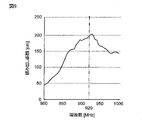
- FIG. 9 is a graph showing the communication characteristics of the container 1 having the RFID module 5 according to the first embodiment. Even in the UHF band from 860 MHz to 960 MHz, it has a communication distance of about 150 cm or more, and in particular, it has a communication distance of about 200 cm around 920 MHz.
- the slot 9 is formed in the seal portion 4, the slot is formed at a position that does not overlap with the containing portion 2 in which the contents of the container 1 are contained. As a result, deterioration of the reading distance can be reduced even if the content is metal or water.
- the container 1 can obtain communication characteristics as a slot antenna.
- the length of the slot 9 has a physical length of half the wavelength of the electromagnetic wave of the communication frequency. As a result, the maximum communication distance as a slot antenna is often obtained.
- FIG. 10 is a partial plan view of a container 1A in Modification 1 of Embodiment 1.
- FIG. A container 1A in Modification 1 of Embodiment 1 has a configuration in which slot 9 and through-hole 11 of container 1 of Embodiment 1 are integrally formed.
- Other configurations of Modification 1 of Embodiment 1 are substantially the same as those of container 1 of Embodiment 1.
- FIG. Even with such a configuration there is no change in communication characteristics, so the container 1A of Modification 1 of Embodiment 1 can obtain the same effects as the container 1 of Embodiment 1.
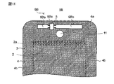
- FIG. 11 is a partial plan view of a container 1B in Modification 2 of Embodiment 1.
- FIG. 1B according to Modification 2 of Embodiment 1 the through hole 11 is formed inside (center side) of the container 1B with respect to the slot 9B. As a result, deformation of the container 1 can be reduced when the support rod is passed through the through hole 11 and the container 1 is suspended.
- the slot 9B may have a shape in which a plurality of cavities are combined instead of having a single cavity shape.
- the slot 9B includes, for example, a first cavity 9Ba, a second cavity 9Bb, and a third cavity 9bc having a smaller width than the first cavity 9Ba and the second cavity 9Bb.
- the first cavity 9Ba, the second cavity 9Bb, and the third cavity 9Bc for example, each have a rectangular shape in plan view.
- the third cavity portion 9bc communicates the first cavity portion 9Ba and the second cavity portion 9bb.
- the RFID module 5 is arranged across the third cavity 9bc.
- Other configurations of Modification 2 of Embodiment 1 are substantially the same as those of container 1 of Embodiment 1. FIG. Even with such a configuration, the communication characteristics are not changed, so the container 1B of the second modification of the first embodiment can obtain the same effect as the container 1 of the first embodiment.
- FIG. 12 is a partial plan view of a container 1C in Modification 3 of Embodiment 1.
- FIG. 1C according to Modification 3 of Embodiment 1 the through holes 11 are formed outside (on the outer edge side) of the container 1C relative to the slots 9 .
- Other configurations of the third modification of the first embodiment are substantially the same as the container 1 of the first embodiment. Even with such a configuration, there is no change in communication characteristics, so the container 1C of Modification 3 of Embodiment 1 can obtain the same effects as the container 1 of Embodiment 1.
- FIG. 13 is a partial plan view of a container 1D in Modification 4 of Embodiment 1.
- FIG. A container 1D according to Modification 4 of Embodiment 1 has a configuration in which one end of slot 9 is open in the case of container 1B according to Modification 2 of Embodiment 1.
- FIG. The slot 9D of the container 1D has a first cavity 9Da, a second cavity 9Db and a third cavity 9Dc, and one end of the second cavity 9Db is open. Therefore, the slot 9D forms an inverted F antenna on the metal layer 7 of the first seal portion 4a. Even with such a configuration, the container 1D of Modification 4 of Embodiment 1 can obtain the same effects as the container 1 of Embodiment 1.
- notches 17 are formed on both sides of the container 1D.
- the user can tear the wrapping material 3 through the notch 17 just to cut the upper part of the chuck 2a.
- the cut first seal portion 4a is communicable, for example, by arranging the reader device of the RFID module 5 in a trash can in which the cut first seal portion 4a is discarded, , the number of opened containers 1D can also be detected.
- FIG. 15 is a partial plan view of a container 1E in Modification 5 of Embodiment 1.
- FIG. 15 is a partial plan view of a container 1E in Modification 5 of Embodiment 1.
- FIG. 1F according to Modification 5 of Embodiment 1 in the first sealing portion 4a of the container 1D according to Modification 4 of Embodiment 1, the upper side of the packaging material 3 and the first cavity 9Da and the third cavity 9Dc , a slit 19 extending along the longitudinal direction of the slot 9D is further formed.
- the container 1E of Modification 5 of Embodiment 1 has the same effects as the container D of Modification 5 of Embodiment 1. Obtainable.
- FIG. 16 is a partial plan view of the container 1F in Modification 6 of Embodiment 1.
- the slot 9F is provided with a first cavity 9Fa, a second cavity 9Fb and a third cavity 9Fc, and one end of the first cavity 9Fa extends along the side of the packaging material 3. It is opened by communicating with a notch 18 formed in . As a result, the user can easily disable communication with the RFID module 5 by tearing the slot 9F starting from the notch 18 .
- An inverted F antenna is formed in the metal layer 7 of the first seal portion 4a by the slot 9F.
- the container 1F of Modified Example 6 of Embodiment 1 having such slots 9F can obtain the same effect as the container 1 of Embodiment 1.
- FIG. 17 is a partial plan view of the container 1G in Modification 7 of Embodiment 1.
- FIG. A container 1G in Modification 7 of Embodiment 1 is different from the container 1F in Modification 6 of Embodiment 1 in that the lower ends of the first cavity portion 9Fa and the second cavity portion 9Fb of the slot 9F and the lower end of the through hole 11 are on the same straight line. placed above.
- Other configurations of the seventh modification of the first embodiment are substantially the same as the container 1F of the sixth modification of the first embodiment. Even with such a configuration, the container 1G of the seventh modification of the first embodiment can obtain the same effect as the container 1F of the sixth modification of the first embodiment.
- FIG. 18 is a partial plan view of a container 1H in Modification 8 of Embodiment 1.
- FIG. A container 1H in Modification 8 of Embodiment 1 has a slit 19 as in the configuration of Modification 5 of Embodiment 1, slot 9H includes cavity 9Hb and cavity 9Hc, and one end of cavity 9Hc is , openings at the sides of the packaging material 3 . Also, one end of the hollow portion 9Hb connected to the other end of the hollow portion 9Hc is open to the upper side of the packaging material 3 . Therefore, the metal layer 7 of the first seal portion 4a forms a monopole antenna due to the slot 9H. Even with such a configuration, the container 1H of Modification 8 of Embodiment 1 can obtain the same effects as the container 1 of Embodiment 1.
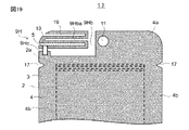
- FIG. 19 is a partial plan view of a container 1J in Modification 9 of Embodiment 1.
- FIG. A container 1J according to Modification 9 of Embodiment 1 has two slits 19 extending in parallel with the container 1H of Modification 8 of Embodiment 1, and a hollow portion 9Hb is formed between the two slits 19.
- a hollow portion 9Hba extending linearly from the side is formed.
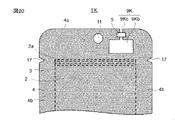
- FIG. 20 is a partial plan view of the container 1K in Modification 10 of Embodiment 1.
- FIG. The slot 9K of the container 1K in Modification 10 of Embodiment 1 includes a hollow portion 9Kb and a hollow portion 9Kc, and one end of the hollow portion 9Kc opens to the upper side of the packaging material 3 . The other end of the hollow portion 9Kc communicates with the hollow portion 9Kb. Even with such a configuration, the container 1L of the eleventh modification of the first embodiment can obtain the same effects as the container 1 of the first embodiment.
- FIG. 21 is a partial plan view of the container 1L in Modification 11 of Embodiment 1.
- FIG. 1 L of containers in the modification 11 of Embodiment 1 are not provided with the through-hole 11.
- FIG. 1 L of containers in the modification 11 of Embodiment 1 are not provided with the through-hole 11.
- FIG. 1 L has a first cavity 9La, a second cavity 9Lb and a third cavity 9Lc. Even with such a configuration, the container 1L of the eleventh modification of the first embodiment can obtain the same effects as the container 1 of the first embodiment.
- Embodiment 2 A container 1 according to Embodiment 2 of the present invention will be described below.
- the difference between the container 1 of Embodiment 2 and the container 1 of Embodiment 1 is the difference in sheet resistance of the metal layer 7 . This difference will be mainly described below. In the description of the second embodiment, descriptions of elements having the same configurations, actions, and functions as those of the first embodiment may be omitted in order to avoid overlapping descriptions.
- the container 1 of Embodiment 2 has the same configuration as the RFID module 5 of Embodiment 1 except for the points described below.
- the sheet resistance of the metal layer 7 of the container 1 of the second embodiment is greater than the sheet resistance of the metal layer 7 of the container 1 of the first embodiment.
- the sheet resistance of the metal layer 7 is high, the following problems that do not occur in the container 1 of the first embodiment occur.
- the entire metal layer 7 around the slot 9 as an antenna electrode causes a resonance phenomenon and radiates electromagnetic waves.
- the thickness of the metal layer 7 in Embodiment 1 is, for example, greater than 5 ⁇ m and 40 ⁇ m or less, and the sheet resistance of the metal layer 7 is 0.05 ⁇ / ⁇ or less.
- the metal layer of the container is usually formed to prevent food oxidation and improve design.
- a metal layer (vapor-deposited film) having this thickness for example, an aluminum vapor-deposited film, has a small film thickness and therefore has a large sheet resistance, for example, about 0.5 ⁇ to 50 ⁇ / ⁇ .
- the resistance value of the matching circuit section between the RFIC and the antenna is the same thickness as the metal layer, the resistance value of the matching circuit section increases, the matching loss increases, and it does not work as an RFID module.
- an antenna electrode made of a thin metal layer cannot cause electromagnetic wave radiation due to a (series) resonance phenomenon. to shield.
- This current is also called eddy current.
- the eddy current flows, the current component flowing in the metal layer is not due to the resonance phenomenon of the antenna electrode, so it can handle all frequency components regardless of the electrode pattern shape.
- This eddy current is known as an effect of metal shielding, but it is not commonly used as an antenna.
- the RFID module 5 Since the RFID module 5 has a parallel resonance circuit RC1 as a filter circuit that transmits only the current of the unique resonance frequency to the RFIC 23, the eddy current is frequency-selected, current flows through the RFIC 23, and energy is transmitted.
- RC1 parallel resonance circuit
- the high sheet resistance of the metal layer 7 is caused not only by the thickness of the metal layer 7 but also by the manufacturing method of the metal layer 7 .
- the sheet resistance may be 0.5 ⁇ or more. Even in such a case, wireless communication can be performed with the container 1 of the second embodiment.
- the present invention is not limited to the above embodiments, and can be modified as follows.
- the container 1 is a container using two wrapping materials, but it is not limited to this.
- the container 1 may be a container in which a single packaging material is folded back and its three sides are joined together, or a self-supporting container with a wider bottom using three or more packaging materials.
- the slots 9 and slits 19 are hollow portions penetrating the packaging material 3, but the present invention is not limited to this.
- a resin film may be attached to the slots 9 and the slits 19 to increase the strength of the container 1 .
- the base material 6 of the packaging material 3 may be left in the areas of the slots 9 and slits 19, leaving only the metal layer 7 hollow.
- the communication frequency band is the UHF band, but it is not limited to this. It may be configured to perform wireless communication using a high-frequency signal having a frequency (carrier frequency) for communication in the HF band. In this case, the entire length of the metal layer 7 perpendicular to the slot 9 is designed to receive high frequency signals in the HF band.
- the HF band is a frequency band from 13 MHz to 15 MHz.
Landscapes
- Engineering & Computer Science (AREA)
- Computer Hardware Design (AREA)
- Microelectronics & Electronic Packaging (AREA)
- Physics & Mathematics (AREA)
- General Physics & Mathematics (AREA)
- Theoretical Computer Science (AREA)
- Mechanical Engineering (AREA)
- Waveguide Aerials (AREA)
- Bag Frames (AREA)
- Details Of Aerials (AREA)
Priority Applications (1)
| Application Number | Priority Date | Filing Date | Title |
|---|---|---|---|
| JP2023510800A JP7294562B2 (ja) | 2021-04-01 | 2022-03-10 | Rfidモジュールを備えた容器 |
Applications Claiming Priority (2)
| Application Number | Priority Date | Filing Date | Title |
|---|---|---|---|
| JP2021-062879 | 2021-04-01 | ||
| JP2021062879 | 2021-04-01 |
Publications (1)
| Publication Number | Publication Date |
|---|---|
| WO2022209714A1 true WO2022209714A1 (ja) | 2022-10-06 |
Family
ID=83456082
Family Applications (1)
| Application Number | Title | Priority Date | Filing Date |
|---|---|---|---|
| PCT/JP2022/010700 Ceased WO2022209714A1 (ja) | 2021-04-01 | 2022-03-10 | Rfidモジュールを備えた容器 |
Country Status (2)
| Country | Link |
|---|---|
| JP (1) | JP7294562B2 (https=) |
| WO (1) | WO2022209714A1 (https=) |
Citations (7)
| Publication number | Priority date | Publication date | Assignee | Title |
|---|---|---|---|---|
| CN102372120A (zh) * | 2010-08-16 | 2012-03-14 | 姜文波 | 兼作rfid标签的金属箔纸及其制造方法和包装盒 |
| WO2013157288A1 (ja) * | 2012-04-18 | 2013-10-24 | 株式会社 村田製作所 | 通信装置 |
| WO2015020042A1 (ja) * | 2013-08-09 | 2015-02-12 | 株式会社リコー | 無線icタグ付き包装体および無線icタグ付き包装体の製造方法 |
| JP2015060260A (ja) * | 2013-09-17 | 2015-03-30 | 株式会社リコー | 通信装置、通信システム、及び通信装置の使用方法 |
| WO2016084658A1 (ja) * | 2014-11-27 | 2016-06-02 | 株式会社 村田製作所 | Rficモジュールおよびそれを備えるrfidタグ |
| JP2020021389A (ja) * | 2018-08-03 | 2020-02-06 | 大日本印刷株式会社 | Rfタグ付き包装体 |
| JP6787538B1 (ja) * | 2019-07-31 | 2020-11-18 | 株式会社村田製作所 | Rficモジュール及びrfidタグ |
Family Cites Families (2)
| Publication number | Priority date | Publication date | Assignee | Title |
|---|---|---|---|---|
| TWI446269B (zh) * | 2009-12-03 | 2014-07-21 | Ind Tech Res Inst | 無線通訊裝置 |
| TWI433389B (zh) * | 2010-04-22 | 2014-04-01 | Taiwan Lamination Ind Inc | Packaging bag with radio frequency identification capability and its manufacturing method |
-
2022
- 2022-03-10 WO PCT/JP2022/010700 patent/WO2022209714A1/ja not_active Ceased
- 2022-03-10 JP JP2023510800A patent/JP7294562B2/ja active Active
Patent Citations (7)
| Publication number | Priority date | Publication date | Assignee | Title |
|---|---|---|---|---|
| CN102372120A (zh) * | 2010-08-16 | 2012-03-14 | 姜文波 | 兼作rfid标签的金属箔纸及其制造方法和包装盒 |
| WO2013157288A1 (ja) * | 2012-04-18 | 2013-10-24 | 株式会社 村田製作所 | 通信装置 |
| WO2015020042A1 (ja) * | 2013-08-09 | 2015-02-12 | 株式会社リコー | 無線icタグ付き包装体および無線icタグ付き包装体の製造方法 |
| JP2015060260A (ja) * | 2013-09-17 | 2015-03-30 | 株式会社リコー | 通信装置、通信システム、及び通信装置の使用方法 |
| WO2016084658A1 (ja) * | 2014-11-27 | 2016-06-02 | 株式会社 村田製作所 | Rficモジュールおよびそれを備えるrfidタグ |
| JP2020021389A (ja) * | 2018-08-03 | 2020-02-06 | 大日本印刷株式会社 | Rfタグ付き包装体 |
| JP6787538B1 (ja) * | 2019-07-31 | 2020-11-18 | 株式会社村田製作所 | Rficモジュール及びrfidタグ |
Also Published As
| Publication number | Publication date |
|---|---|
| JP7294562B2 (ja) | 2023-06-20 |
| JPWO2022209714A1 (https=) | 2022-10-06 |
Similar Documents
| Publication | Publication Date | Title |
|---|---|---|
| JP6590122B1 (ja) | Rfidタグ、および、rfidタグが取り付けられた物品 | |
| JP7074275B1 (ja) | Rfidモジュールを備えた容器 | |
| US8576124B2 (en) | RFID transponder, in particular for assembly on metal and manufacturing method therefor | |
| US12327155B2 (en) | Container provided with RFID module and method for manufacturing container provided with RFID module | |
| JP6583589B2 (ja) | 無線通信デバイス | |
| US10726322B2 (en) | Wireless communication device and article equipped with the same | |
| US8770489B2 (en) | Radio communication device | |
| US10476147B2 (en) | Antenna device and method of manufacturing the same | |
| JP2012253699A (ja) | 無線通信デバイス、その製造方法及び無線通信デバイス付き金属物品 | |
| WO2012032974A1 (ja) | Rfidモジュールおよびrfidデバイス | |
| JP2011193245A (ja) | アンテナ装置、無線通信デバイス及び無線通信端末 | |
| US10380478B2 (en) | Wireless communication device and wireless communication module manufacturing method | |
| JP7294562B2 (ja) | Rfidモジュールを備えた容器 | |
| US20170300801A1 (en) | Rfid tag and high frequency circuit | |
| JP7201137B2 (ja) | Rfidモジュールを備えた容器 | |
| JP7239073B2 (ja) | Rfidモジュールを備えた容器 | |
| JP7197065B2 (ja) | Rfidモジュールを備えた容器 | |
| JP2012252664A (ja) | 無線通信デバイス、その製造方法及び無線通信デバイス付き金属物品 | |
| US12033022B2 (en) | RFID auxiliary antenna device | |
| JP5886100B2 (ja) | 無線icタグ | |
| JP2006270448A (ja) | 小電力無線装置 | |
| JP6658973B2 (ja) | 無線通信デバイス |
Legal Events
| Date | Code | Title | Description |
|---|---|---|---|
| 121 | Ep: the epo has been informed by wipo that ep was designated in this application |
Ref document number: 22779935 Country of ref document: EP Kind code of ref document: A1 |
|
| ENP | Entry into the national phase |
Ref document number: 2023510800 Country of ref document: JP Kind code of ref document: A |
|
| NENP | Non-entry into the national phase |
Ref country code: DE |
|
| 122 | Ep: pct application non-entry in european phase |
Ref document number: 22779935 Country of ref document: EP Kind code of ref document: A1 |