WO2022209714A1 - Rfidモジュールを備えた容器 - Google Patents
Rfidモジュールを備えた容器 Download PDFInfo
- Publication number
- WO2022209714A1 WO2022209714A1 PCT/JP2022/010700 JP2022010700W WO2022209714A1 WO 2022209714 A1 WO2022209714 A1 WO 2022209714A1 JP 2022010700 W JP2022010700 W JP 2022010700W WO 2022209714 A1 WO2022209714 A1 WO 2022209714A1
- Authority
- WO
- WIPO (PCT)
- Prior art keywords
- container
- rfid module
- metal layer
- slot
- module according
- Prior art date
Links
- 229910052751 metal Inorganic materials 0.000 claims abstract description 89
- 239000002184 metal Substances 0.000 claims abstract description 89
- 238000004891 communication Methods 0.000 claims abstract description 50
- 239000005022 packaging material Substances 0.000 claims abstract description 35
- 229920005989 resin Polymers 0.000 claims abstract description 10
- 239000011347 resin Substances 0.000 claims abstract description 10
- 239000010410 layer Substances 0.000 claims description 102
- 239000000758 substrate Substances 0.000 claims description 27
- 230000002093 peripheral effect Effects 0.000 claims description 5
- 239000011241 protective layer Substances 0.000 claims description 3
- 239000000463 material Substances 0.000 abstract description 16
- 230000004048 modification Effects 0.000 description 68
- 238000012986 modification Methods 0.000 description 68
- 239000004020 conductor Substances 0.000 description 62
- 239000010408 film Substances 0.000 description 15
- 230000008859 change Effects 0.000 description 12
- 230000000694 effects Effects 0.000 description 11
- 230000001681 protective effect Effects 0.000 description 10
- 238000013461 design Methods 0.000 description 8
- 238000007789 sealing Methods 0.000 description 8
- RYGMFSIKBFXOCR-UHFFFAOYSA-N Copper Chemical compound [Cu] RYGMFSIKBFXOCR-UHFFFAOYSA-N 0.000 description 4
- 239000000853 adhesive Substances 0.000 description 4
- 230000001070 adhesive effect Effects 0.000 description 4
- 239000003990 capacitor Substances 0.000 description 4
- 230000006866 deterioration Effects 0.000 description 4
- 229910052782 aluminium Inorganic materials 0.000 description 3
- XAGFODPZIPBFFR-UHFFFAOYSA-N aluminium Chemical compound [Al] XAGFODPZIPBFFR-UHFFFAOYSA-N 0.000 description 3
- 239000000470 constituent Substances 0.000 description 3
- 239000011889 copper foil Substances 0.000 description 3
- 238000010586 diagram Methods 0.000 description 3
- -1 polypropylene Polymers 0.000 description 3
- 239000004743 Polypropylene Substances 0.000 description 2
- 239000007788 liquid Substances 0.000 description 2
- 230000005404 monopole Effects 0.000 description 2
- 238000000059 patterning Methods 0.000 description 2
- 230000000149 penetrating effect Effects 0.000 description 2
- 238000000206 photolithography Methods 0.000 description 2
- 229920001721 polyimide Polymers 0.000 description 2
- 229920001155 polypropylene Polymers 0.000 description 2
- 238000007639 printing Methods 0.000 description 2
- 238000012545 processing Methods 0.000 description 2
- 230000009467 reduction Effects 0.000 description 2
- 238000003860 storage Methods 0.000 description 2
- 239000004698 Polyethylene Substances 0.000 description 1
- 239000004642 Polyimide Substances 0.000 description 1
- 230000005540 biological transmission Effects 0.000 description 1
- 239000003795 chemical substances by application Substances 0.000 description 1
- 238000010276 construction Methods 0.000 description 1
- 229910052802 copper Inorganic materials 0.000 description 1
- 239000010949 copper Substances 0.000 description 1
- 239000012787 coverlay film Substances 0.000 description 1
- 229920001971 elastomer Polymers 0.000 description 1
- 239000000806 elastomer Substances 0.000 description 1
- 230000005672 electromagnetic field Effects 0.000 description 1
- 238000005516 engineering process Methods 0.000 description 1
- 239000005038 ethylene vinyl acetate Substances 0.000 description 1
- 230000004907 flux Effects 0.000 description 1
- 239000011888 foil Substances 0.000 description 1
- 238000007646 gravure printing Methods 0.000 description 1
- 239000012943 hotmelt Substances 0.000 description 1
- 238000007641 inkjet printing Methods 0.000 description 1
- 238000005304 joining Methods 0.000 description 1
- 238000004519 manufacturing process Methods 0.000 description 1
- 239000007769 metal material Substances 0.000 description 1
- 239000010813 municipal solid waste Substances 0.000 description 1
- 238000007645 offset printing Methods 0.000 description 1
- 230000003647 oxidation Effects 0.000 description 1
- 238000007254 oxidation reaction Methods 0.000 description 1
- 230000003071 parasitic effect Effects 0.000 description 1
- 229920003223 poly(pyromellitimide-1,4-diphenyl ether) Polymers 0.000 description 1
- 229920000573 polyethylene Polymers 0.000 description 1
- 229920002635 polyurethane Polymers 0.000 description 1
- 239000004814 polyurethane Substances 0.000 description 1
- 230000005855 radiation Effects 0.000 description 1
- 238000007790 scraping Methods 0.000 description 1
- 238000004904 shortening Methods 0.000 description 1
- 229920003002 synthetic resin Polymers 0.000 description 1
- 239000000057 synthetic resin Substances 0.000 description 1
- 238000007740 vapor deposition Methods 0.000 description 1
- XLYOFNOQVPJJNP-UHFFFAOYSA-N water Substances O XLYOFNOQVPJJNP-UHFFFAOYSA-N 0.000 description 1
- 238000004804 winding Methods 0.000 description 1
Images


Classifications
-
- B—PERFORMING OPERATIONS; TRANSPORTING
- B65—CONVEYING; PACKING; STORING; HANDLING THIN OR FILAMENTARY MATERIAL
- B65D—CONTAINERS FOR STORAGE OR TRANSPORT OF ARTICLES OR MATERIALS, e.g. BAGS, BARRELS, BOTTLES, BOXES, CANS, CARTONS, CRATES, DRUMS, JARS, TANKS, HOPPERS, FORWARDING CONTAINERS; ACCESSORIES, CLOSURES, OR FITTINGS THEREFOR; PACKAGING ELEMENTS; PACKAGES
- B65D65/00—Wrappers or flexible covers; Packaging materials of special type or form
- B65D65/38—Packaging materials of special type or form
- B65D65/40—Applications of laminates for particular packaging purposes
-
- G—PHYSICS
- G06—COMPUTING; CALCULATING OR COUNTING
- G06K—GRAPHICAL DATA READING; PRESENTATION OF DATA; RECORD CARRIERS; HANDLING RECORD CARRIERS
- G06K19/00—Record carriers for use with machines and with at least a part designed to carry digital markings
- G06K19/06—Record carriers for use with machines and with at least a part designed to carry digital markings characterised by the kind of the digital marking, e.g. shape, nature, code
- G06K19/067—Record carriers with conductive marks, printed circuits or semiconductor circuit elements, e.g. credit or identity cards also with resonating or responding marks without active components
- G06K19/07—Record carriers with conductive marks, printed circuits or semiconductor circuit elements, e.g. credit or identity cards also with resonating or responding marks without active components with integrated circuit chips
- G06K19/077—Constructional details, e.g. mounting of circuits in the carrier
-
- H—ELECTRICITY
- H01—ELECTRIC ELEMENTS
- H01Q—ANTENNAS, i.e. RADIO AERIALS
- H01Q13/00—Waveguide horns or mouths; Slot antennas; Leaky-waveguide antennas; Equivalent structures causing radiation along the transmission path of a guided wave
- H01Q13/10—Resonant slot antennas
-
- H—ELECTRICITY
- H01—ELECTRIC ELEMENTS
- H01Q—ANTENNAS, i.e. RADIO AERIALS
- H01Q19/00—Combinations of primary active antenna elements and units with secondary devices, e.g. with quasi-optical devices, for giving the antenna a desired directional characteristic
- H01Q19/02—Details
Definitions
- the present invention relates to a container equipped with an RFID module, particularly a container equipped with an RFID module using RFID (Radio Frequency Identification) technology for non-contact data communication using an induced electromagnetic field or radio waves.
- RFID Radio Frequency Identification
- RFID tags which are wireless communication devices
- An RFID tag together with RFIC (Radio-Frequency Integrated Circuit)
- RFIC Radio-Frequency Integrated Circuit
- a metal material such as an antenna pattern formed on an insulating substrate such as paper or resin.
- the RFID tag will be affected and will not be able to communicate.
- Patent Document 1 proposes a configuration in which an RFID tag that is compatible with metal formed on a part of the container is provided so as not to impair the design.
- the RFID tag disclosed in Patent Document 1 has an RFIC chip and an antenna pattern, and a metal layer cannot be formed on the container in these areas. Therefore, there is a demand for a container having an RFID module that suppresses a reduction in the degree of design freedom.
- An object of the present invention is to provide a container having an RFID module that suppresses deterioration of design in a container on which a metal layer is formed.
- a container of one embodiment of the present invention is a container provided with an RFID module, which includes a packaging material having a resin base material and a metal layer formed on the base material, and a peripheral edge of the packaging material.
- the RFID module includes an RFIC element, a filter circuit for transmitting a current due to electromagnetic waves having a unique resonance frequency, which is a communication frequency, to the RFIC element, and first and second electrodes connected to the filter circuit.
- the first electrode of the RFID module and the metal layer are electrically connected.
- the second electrode of the RFID module and the metal layer are electrically connected across the slot by the RFID module.
- the present invention it is possible to provide a container having an RFID module that suppresses deterioration in design in a container on which a metal layer is formed.
- FIG. 1 is a plan view of a container having an RFID module according to Embodiment 1;
- FIG. 6A is a plan view of a conductor pattern formed on the substrate of the RFID module;
- FIG. 6B is a plan view of the conductor pattern formed on the bottom surface of the substrate; perspective plan view from above Sectional view of arrow VII in FIG.
- FIG. 11 is a plan view of the cut first seal portion of the container in the modified example of the first embodiment; Partial plan view of the container in the modification of Embodiment 1 Partial plan view of the container in the modification of Embodiment 1 Partial plan view of the container in the modification of Embodiment 1 Partial plan view of the container in the modification of Embodiment 1 Partial plan view of the container in the modification of Embodiment 1 Partial plan view of the container in the modification of Embodiment 1 Partial plan view of the container in the modification of Embodiment 1 Partial plan view of the container in the modification of Embodiment 1 Partial plan view of the container in the modification of Embodiment 1
- a container according to one aspect of the present invention is a container provided with an RFID module, the packaging material having a resin base material and a metal layer formed on the base material, and the peripheral edge of the packaging material
- the container includes a container for containing contents inside the seals joined to each other, and a slot formed in the seals.
- the RFID module includes an RFIC element, a filter circuit for transmitting a current due to electromagnetic waves having a unique resonance frequency, which is a communication frequency, to the RFIC element, and first and second electrodes connected to the filter circuit.
- the first electrode of the RFID module and the metal layer are electrically connected.
- the second electrode of the RFID module and the metal layer are electrically connected across the slot by the RFID module.
- the container of this aspect uses the metal layer formed on the base material of the container as an antenna, in the container in which the metal layer is formed, the RFID module can be attached to the container while suppressing the reduction in the degree of freedom of design. can be done.
- the container may have a through hole formed in the sealing portion. Since the container has a through hole, the container can be suspended by passing the support rod through the through hole.
- the through hole may be formed on the extension of the slot in the direction in which the slot extends. Thereby, the through holes and the slots can be formed at the same time, and the processing cost can be reduced.
- the through-hole may be formed outside the container rather than the slot. This can reduce deformation of the container when the support rod is passed through the through hole.
- the through hole may be formed inside the container rather than the slot.
- the metal layer when the metal layer is irradiated with an electromagnetic wave of a communication frequency, a current may flow in the direction of circling the slot. In this way, the metal layer functions as a slot antenna, so communication characteristics of a slot antenna can be obtained.
- the length of the slot may have the physical length of half the wavelength of the electromagnetic wave at the communication frequency. In this case, the maximum communication distance as a slot antenna is often obtained.
- the filter circuit may be an LC parallel resonant circuit. As a result, a current with a frequency that matches the RFIC can be passed through the RFIC.
- the filter circuit has a coil formed on the substrate, and the coil may be covered with a protective layer. Thereby, the dielectric constant of the coil can be fixed, and the influence of the dielectric inside the container can be prevented.
- the coil of the filter circuit may have a figure-of-eight shape. This makes it difficult for the magnetic field of the coil to leak to the outside, and makes it difficult for the inductance value of the coil to change due to external factors.
- the sheet resistance of the metal layer may be 0.5 ⁇ / ⁇ or more. Even with this configuration, since the RFID module has a filter circuit, the eddy current generated in the metal layer can be used to flow to the RFIC.
- the thickness of the metal layer may be 1 nm or more and 1 ⁇ m or less. Even with this configuration, since the RFID module has a filter circuit, the eddy current generated in the metal layer can be used to flow to the RFIC.
- the electrical lengths of the antenna pattern and the conductor pattern are longer than their physical lengths.
- the electrical length is a length that takes into account wavelength shortening due to relative permittivity and parasitic reactance components.
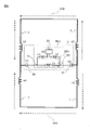
- FIG. 1 is an overall perspective view of a container 1 having an RFID module 5 according to Embodiment 1 of the present invention.
- 2 is a cross-sectional view taken along arrow II in FIG. 1
- FIG. 3 is a cross-sectional view taken along arrow III in FIG.
- the container 1 of Embodiment 1 includes a packaging material 3 , an RFID module 5 attached to the packaging material 3 , and a slot 9 formed in the packaging material 3 .
- one side of the container 1 is defined as an upper side
- a side opposite to the upper side is defined as a lower side
- a side connecting the upper side and the lower side is defined as a lateral side.
- the through holes 11 are arranged on the upper side.
- the container 1 is, for example, a bag-like container formed by joining, for example, thermocompression bonding the peripheral edge portions of two flat packaging materials 3 as shown in FIG.
- the container 1 includes a storage portion 2 for storing contents inside, and a seal portion 4 to which packaging materials 3 on the front and back sides are respectively joined.
- the seal portion 4 has a first seal portion 4 a above the housing portion 2 and second seal portions 4 b laterally and below the housing portion 2 .
- the container 1 can have the first seal portion 4 a cut off from the end of the packaging material 3 . Since the container 1 has the chuck 2a on the upper part of the housing part 2, the container 1 can be opened and closed even after the first seal part 4a is cut off from the container 1. As shown in FIG.
- the packaging material 3 includes a base material 6 , a metal layer 7 laminated on the base material 6 , a printed layer 8 laminated on the metal layer 7 , and a cover layer 10 formed on the printed layer 8 .
- the base material 6 is a resin layer, for example polypropylene.
- the metal layer 7 is made of a film of a conductive material such as aluminum foil or copper foil, and is formed, for example, by attaching a metal sheet. A communication distance can be increased by using a metal having a low resistance value, such as aluminum or copper, as the metal layer 7 .
- the thickness of the metal layer 7 is, for example, greater than 5 ⁇ m and equal to or less than 40 ⁇ m.
- the metal layer 7 is formed on the entire surface of the packaging material 3 except for the slots 9 in FIG. It may be partially formed in the first seal portion 4a.
- the printed layer 8 is a resin layer printed using ink.
- the printing layer 8 is, for example, polyethylene, and characters and figures are printed thereon by inkjet printing, gravure printing, offset printing, or the like. Note that the packaging material 3 may not have the printed layer 8 .
- the cover layer 10 is a layer that protects the metal layer 7 and the printed layer 8 from moisture and dirt.
- the cover layer 10 is a resin layer, such as polypropylene.
- the through hole 11 is a hole for passing the container 1 through, for example, a support rod. As a result, the container 1 can be displayed by hanging it from a rod.
- the through hole 11 is formed in the seal portion 4, for example, on the extension of the slot 9 in the direction in which the slot 9 extends in the first seal portion 4a. As a result, the slot 9 and the through hole 11 can be formed simultaneously using a mold, and the processing cost can be reduced. Note that the container 1 may not have the through holes 11 .
- the slot 9 is a groove formed at least within the area of the metal layer 7 . As shown in FIG. 2, a groove penetrating the packaging material 3 may be used.
- the slots 9 may be formed at the same time when the through holes 11 are formed using a mold, or may be formed by scraping the metal layer 7 with, for example, sandpaper.
- the slot 9 may be formed in the second sealing portion 4b of the packaging material 3.
- the communication distance is maximized.
- the container 1 is irradiated with an electromagnetic wave having a communication frequency, communication is performed in a direction circulating the slot 9 so as to reciprocate from the RFID module 5 positioned at the center of the slot 9 in the longitudinal direction to the ends of the two slots 9 respectively. It resonates with the frequency and current Ir flows (see FIG. 1).
- the width W of the slot 9 is, for example, 1 mm.
- the RFID module 5 is a wireless communication device configured to wirelessly communicate (transmit and receive) using high-frequency signals having a communication frequency (carrier frequency).
- the RFID module 5 is configured, for example, to wirelessly communicate with a high-frequency signal having a frequency for UHF band communication.
- the UHF band is a frequency band from 860 MHz to 960 MHz.
- FIG. 4 is a perspective plan view of the RFID module
- FIG. 5 is a cross-sectional view taken along arrow V in FIG. 6 shows a plan view of the conductor pattern formed on the substrate of the RFID module
- FIG. 6a is a plan view of the conductor pattern formed on the upper surface of the substrate of the RFID module
- FIG. 6b is a plan view of the conductor pattern formed on the lower surface of the substrate.
- 1 is a perspective plan view of a conductor pattern seen from above
- FIG. 7 is a cross-sectional view taken along line VII in FIG. 4.
- FIG. In the drawings, the XYZ coordinate system is intended to facilitate understanding of the invention and is not intended to limit the invention.
- the X-axis direction indicates the longitudinal direction of the RFID module 5
- the Y-axis direction indicates the depth (width) direction
- the Z-axis direction indicates the thickness direction.
- the X, Y and Z directions are orthogonal to each other.
- the printing layer 8 and the cover layer 10 of the packaging material 3 on the back side and the packaging material 3 on the front side are omitted.
- the RFID module 5 is attached across the slot 9 to the upper surface of the packaging material 3 via double-sided tape or adhesive 15 such as synthetic resin.
- the RFID module 5 includes a substrate 21 and an RFIC 23 mounted on the substrate 21.
- the substrate 21 is, for example, a flexible substrate such as polyimide.
- a protective film 25 is formed on the upper surface of the substrate 21 on which the RFIC 23 is mounted.
- the protective film 25 is, for example, an elastomer such as polyurethane or a hot melt agent such as ethylene vinyl acetate (EVA).
- a protective film 27 is also attached to the lower surface of the substrate 21 .
- the protective film 27 is, for example, a coverlay film such as a polyimide film (Kapton tape).
- a third electrode 33, a fourth electrode 35, a conductor pattern L1a of the main portion of the first inductance element L1, and a conductor pattern L2a of the main portion of the second inductance element L2 are formed on the upper surface of the substrate 21.
- FIG. The third electrode 33 is connected to one end of the conductor pattern L1a
- the fourth electrode 35 is connected to one end of the conductor pattern L2a.
- a first electrode 29 and a second electrode 31 capacitively coupled to the metal layer 7 are formed on the lower surface of the substrate 21 . Further, on the lower surface of the substrate 21, a conductor pattern L1b, which is a part of the first inductance element L1, and conductor patterns L3a, L3b (a conductor pattern surrounded by a two-dot chain line), and L3c of the third inductance element L3 are formed. These conductor patterns are also obtained by patterning copper foil by photolithography, for example.
- the first electrode 29 is connected to one end of the conductor pattern L1b of the first inductance element L1 and one end of the conductor pattern L3a of the third inductance element L3.
- one end of the conductor pattern L2b of the second inductance element L2 and one end of the conductor pattern L3c of the third inductance element L3 are connected to the second electrode 31 .
- a conductor pattern L3b is connected between the other end of the conductor pattern L3a of the third inductance element L3 and the other end of the conductor pattern L3c.
- the other end of the conductor pattern L1b of the first inductance element L1 and the other end of the conductor pattern L1a of the first inductance element L1 are connected via a via conductor V1.
- the other end of the conductor pattern L2b of the second inductance element L2 and the other end of the conductor pattern L2a of the second inductance element L2 are connected via a via conductor V2.
- the RFIC 23 is mounted on the third electrode 33 and the fourth electrode 35 formed on the upper surface of the substrate 21 . That is, the terminal 23 a of the RFIC 23 is connected to the third electrode 33 and the terminal 23 b of the RFIC 23 is connected to the fourth electrode 35 .
- the conductor patterns L3a of the first inductance element L1 and the third inductance element L3 are formed in different layers of the substrate 21, respectively, and arranged so that their coil openings overlap.
- the conductor patterns L3c of the second inductance element L2 and the third inductance element L3 are formed in different layers of the substrate 21, respectively, and arranged such that their coil openings overlap.
- the RFIC 23 is positioned between the conductor pattern L3c of the second inductance element L2 and the third inductance element L3 and the conductor pattern L3a of the first inductance element L1 and the third inductance element L3 on the surface of the substrate 21. do.
- the conductor patterns L1a, L1b, and L3a form a first coil Cr1
- the conductor patterns L2a, L2b, and L3c form a second coil Cr2.
- a first current path CP1 passing through the top and bottom surfaces of the substrate 21 and a second current path CP2 passing through the bottom surface of the substrate 21 are formed.
- the first current path CP1 extends from the first electrode 29 to the second electrode 31 through the branch point N1, the conductor pattern L1b, the conductor pattern L1a, the RFIC 23, the conductor pattern L2a, the conductor pattern L2b, and the branch point N2.
- the second current path CP2 extends from the first electrode 29 to the second electrode 31 through the branch point N1, the conductor pattern L3a, the conductor pattern L3b, the conductor pattern L3c, and the branch point N2.
- the first inductance element L1 is composed of the conductor pattern L1b connected to the conductor pattern L1a via the via conductor V1
- the conductor pattern L2b is composed of the conductor pattern L2a connected to the conductor pattern L2a via the via conductor V2.
- the winding direction of the current flowing through the second inductance element L2 is reversed, and the magnetic field generated by the first inductance element L1 and the magnetic field generated by the second inductance element L2 cancel each other.
- the first current path CP1 and the second current path CP2 are formed in parallel with each other between the first electrode 29 and the second electrode 31, respectively.
- the slot antenna is not suitable as an antenna formed in the container.
- the dielectric constant of the RFID tag increases and the electrical length of the slot becomes longer than half the wavelength of the electromagnetic wave of the communication frequency, which lowers the resonance frequency of the antenna.
- the change in permittivity also changes depending on the distance between the contents and the slot antenna. Therefore, every time the position of the contents changes in the box, the communication characteristics also change, and the reading distance of the RFID tag becomes unstable.
- the frequency design in order to avoid the wavelength change (frequency change) due to the change in the dielectric constant, the frequency design is not based on the length of the slot 9, but the resonance frequency is fixed by the RFID module 5. It can handle frequency changes due to length.
- the RFIC 23 is a small chip, and each coil pattern is wound so that the first coil Cr1 and the second coil Cr2 having a laminated structure cancel out the magnetic field.
- the periphery of the RFIC 23 is fixed at the dielectric constant of the RFID module 5 and is not affected by the dielectric (contents) accommodated in the container 1, so the frequency matching the RFIC 23 does not change.
- the dielectric constant of the substrate 21 between the conductor patterns L1a, L2a and the conductor patterns L3a, L3c is fixed, and there is no change in line-to-line capacitance.
- the conductor patterns L1a and L2a and the conductor patterns L3a and L3c are covered with a protective film 25 and a protective film 27 as protective layers with a fixed dielectric constant, respectively.
- a protective film 25 and a protective film 27 as protective layers with a fixed dielectric constant, respectively.
- the first coil Cr1 and the second coil Cr2 of the RFID module 5 form a figure-of-eight coil. is difficult to leak to the outside. Since the magnetic field of the RFID module 5 hardly leaks, the inductance value does not easily change due to external factors.
- the magnetic flux of the RFID module 5 is also closed, even if metal is contained in the container 1, the change in frequency matching with the RFIC 23 is small.
- FIG. 8 is an equivalent circuit diagram of the RFID module 5. As shown in FIG.
- the first current path CP1 is part of the parallel resonant circuit RC1, which is an LC parallel resonant circuit, and is matched with the radio waves of the communication frequency. is received, a current flows through the RFIC 23 .
- a parallel resonant circuit RC1 is formed in the RFID module 5.
- the parallel resonant circuit RC1 is a loop circuit composed of a first inductance element L1, RFIC 23, a second inductance element L2, and a third inductance element L3.
- the capacitor C1 is composed of the metal layer 7, the printed layer 8, the cover layer 10, the adhesive 15, the protective film 27, and the first electrode 29.
- Capacitor C ⁇ b>2 is composed of metal layer 7 , printed layer 8 , cover layer 10 , adhesive 15 , protective film 27 and second electrode 31 .
- the fourth inductance element L4 is the inductance component of one metal layer 7
- the fifth inductance element L5 is the inductance component of the other metal layer 7.
- the parallel resonant circuit RC1 is designed to perform LC parallel resonance with impedance matching for radio waves at communication frequencies. Thereby, the communication frequency is matched with the RFIC, and the communication distance of the RFID module 5 at the communication frequency can be secured.
- the container 1 of Embodiment 1 is a container 1 having an RFID module 5, and is a packaging material having a resin base material 6 and a metal layer 7 formed on the base material 6. 3 , a containing portion 2 for containing contents inside a sealing portion 4 in which peripheral portions of the packaging material 3 are joined together, and a slot 9 formed in the sealing portion 4 .
- the RFID module 5 includes an RFIC 23, a parallel resonance circuit RC1 as a filter circuit that transmits current due to electromagnetic waves having a unique resonance frequency, which is a communication frequency, to the RFIC 23, and a first electrode 29 and a second electrode connected to the parallel resonance circuit RC1. 31 and.
- the first electrode 29 of the RFID module 5 and the metal layer 7 are electrically connected, the RFID module 5 straddles the slot 9 and the second electrode 31 of the RFID module 5 and the metal layer 7 are electrically connected.
- the metal layer 7 can be used as an antenna, and current is supplied to the RFIC 23 by series resonance. can flow. Therefore, even if the container 1 has the metal layer 7 formed thereon, it is possible to perform wireless communication, and it is possible to provide the container 1 having the RFID module 5 that suppresses deterioration in design.
- the container 1 of the first embodiment can be provided at a lower cost than a conventional container equipped with a metal RFID module.
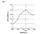
- FIG. 9 is a graph showing the communication characteristics of the container 1 having the RFID module 5 according to the first embodiment. Even in the UHF band from 860 MHz to 960 MHz, it has a communication distance of about 150 cm or more, and in particular, it has a communication distance of about 200 cm around 920 MHz.
- the slot 9 is formed in the seal portion 4, the slot is formed at a position that does not overlap with the containing portion 2 in which the contents of the container 1 are contained. As a result, deterioration of the reading distance can be reduced even if the content is metal or water.
- the container 1 can obtain communication characteristics as a slot antenna.
- the length of the slot 9 has a physical length of half the wavelength of the electromagnetic wave of the communication frequency. As a result, the maximum communication distance as a slot antenna is often obtained.
- FIG. 10 is a partial plan view of a container 1A in Modification 1 of Embodiment 1.
- FIG. A container 1A in Modification 1 of Embodiment 1 has a configuration in which slot 9 and through-hole 11 of container 1 of Embodiment 1 are integrally formed.
- Other configurations of Modification 1 of Embodiment 1 are substantially the same as those of container 1 of Embodiment 1.
- FIG. Even with such a configuration there is no change in communication characteristics, so the container 1A of Modification 1 of Embodiment 1 can obtain the same effects as the container 1 of Embodiment 1.
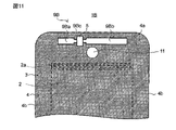
- FIG. 11 is a partial plan view of a container 1B in Modification 2 of Embodiment 1.
- FIG. 1B according to Modification 2 of Embodiment 1 the through hole 11 is formed inside (center side) of the container 1B with respect to the slot 9B. As a result, deformation of the container 1 can be reduced when the support rod is passed through the through hole 11 and the container 1 is suspended.
- the slot 9B may have a shape in which a plurality of cavities are combined instead of having a single cavity shape.
- the slot 9B includes, for example, a first cavity 9Ba, a second cavity 9Bb, and a third cavity 9bc having a smaller width than the first cavity 9Ba and the second cavity 9Bb.
- the first cavity 9Ba, the second cavity 9Bb, and the third cavity 9Bc for example, each have a rectangular shape in plan view.
- the third cavity portion 9bc communicates the first cavity portion 9Ba and the second cavity portion 9bb.
- the RFID module 5 is arranged across the third cavity 9bc.
- Other configurations of Modification 2 of Embodiment 1 are substantially the same as those of container 1 of Embodiment 1. FIG. Even with such a configuration, the communication characteristics are not changed, so the container 1B of the second modification of the first embodiment can obtain the same effect as the container 1 of the first embodiment.
- FIG. 12 is a partial plan view of a container 1C in Modification 3 of Embodiment 1.
- FIG. 1C according to Modification 3 of Embodiment 1 the through holes 11 are formed outside (on the outer edge side) of the container 1C relative to the slots 9 .
- Other configurations of the third modification of the first embodiment are substantially the same as the container 1 of the first embodiment. Even with such a configuration, there is no change in communication characteristics, so the container 1C of Modification 3 of Embodiment 1 can obtain the same effects as the container 1 of Embodiment 1.
- FIG. 13 is a partial plan view of a container 1D in Modification 4 of Embodiment 1.
- FIG. A container 1D according to Modification 4 of Embodiment 1 has a configuration in which one end of slot 9 is open in the case of container 1B according to Modification 2 of Embodiment 1.
- FIG. The slot 9D of the container 1D has a first cavity 9Da, a second cavity 9Db and a third cavity 9Dc, and one end of the second cavity 9Db is open. Therefore, the slot 9D forms an inverted F antenna on the metal layer 7 of the first seal portion 4a. Even with such a configuration, the container 1D of Modification 4 of Embodiment 1 can obtain the same effects as the container 1 of Embodiment 1.
- notches 17 are formed on both sides of the container 1D.
- the user can tear the wrapping material 3 through the notch 17 just to cut the upper part of the chuck 2a.
- the cut first seal portion 4a is communicable, for example, by arranging the reader device of the RFID module 5 in a trash can in which the cut first seal portion 4a is discarded, , the number of opened containers 1D can also be detected.
- FIG. 15 is a partial plan view of a container 1E in Modification 5 of Embodiment 1.
- FIG. 15 is a partial plan view of a container 1E in Modification 5 of Embodiment 1.
- FIG. 1F according to Modification 5 of Embodiment 1 in the first sealing portion 4a of the container 1D according to Modification 4 of Embodiment 1, the upper side of the packaging material 3 and the first cavity 9Da and the third cavity 9Dc , a slit 19 extending along the longitudinal direction of the slot 9D is further formed.
- the container 1E of Modification 5 of Embodiment 1 has the same effects as the container D of Modification 5 of Embodiment 1. Obtainable.
- FIG. 16 is a partial plan view of the container 1F in Modification 6 of Embodiment 1.
- the slot 9F is provided with a first cavity 9Fa, a second cavity 9Fb and a third cavity 9Fc, and one end of the first cavity 9Fa extends along the side of the packaging material 3. It is opened by communicating with a notch 18 formed in . As a result, the user can easily disable communication with the RFID module 5 by tearing the slot 9F starting from the notch 18 .
- An inverted F antenna is formed in the metal layer 7 of the first seal portion 4a by the slot 9F.
- the container 1F of Modified Example 6 of Embodiment 1 having such slots 9F can obtain the same effect as the container 1 of Embodiment 1.
- FIG. 17 is a partial plan view of the container 1G in Modification 7 of Embodiment 1.
- FIG. A container 1G in Modification 7 of Embodiment 1 is different from the container 1F in Modification 6 of Embodiment 1 in that the lower ends of the first cavity portion 9Fa and the second cavity portion 9Fb of the slot 9F and the lower end of the through hole 11 are on the same straight line. placed above.
- Other configurations of the seventh modification of the first embodiment are substantially the same as the container 1F of the sixth modification of the first embodiment. Even with such a configuration, the container 1G of the seventh modification of the first embodiment can obtain the same effect as the container 1F of the sixth modification of the first embodiment.
- FIG. 18 is a partial plan view of a container 1H in Modification 8 of Embodiment 1.
- FIG. A container 1H in Modification 8 of Embodiment 1 has a slit 19 as in the configuration of Modification 5 of Embodiment 1, slot 9H includes cavity 9Hb and cavity 9Hc, and one end of cavity 9Hc is , openings at the sides of the packaging material 3 . Also, one end of the hollow portion 9Hb connected to the other end of the hollow portion 9Hc is open to the upper side of the packaging material 3 . Therefore, the metal layer 7 of the first seal portion 4a forms a monopole antenna due to the slot 9H. Even with such a configuration, the container 1H of Modification 8 of Embodiment 1 can obtain the same effects as the container 1 of Embodiment 1.
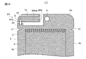
- FIG. 19 is a partial plan view of a container 1J in Modification 9 of Embodiment 1.
- FIG. A container 1J according to Modification 9 of Embodiment 1 has two slits 19 extending in parallel with the container 1H of Modification 8 of Embodiment 1, and a hollow portion 9Hb is formed between the two slits 19.
- a hollow portion 9Hba extending linearly from the side is formed.
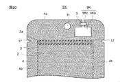
- FIG. 20 is a partial plan view of the container 1K in Modification 10 of Embodiment 1.
- FIG. The slot 9K of the container 1K in Modification 10 of Embodiment 1 includes a hollow portion 9Kb and a hollow portion 9Kc, and one end of the hollow portion 9Kc opens to the upper side of the packaging material 3 . The other end of the hollow portion 9Kc communicates with the hollow portion 9Kb. Even with such a configuration, the container 1L of the eleventh modification of the first embodiment can obtain the same effects as the container 1 of the first embodiment.
- FIG. 21 is a partial plan view of the container 1L in Modification 11 of Embodiment 1.
- FIG. 1 L of containers in the modification 11 of Embodiment 1 are not provided with the through-hole 11.
- FIG. 1 L of containers in the modification 11 of Embodiment 1 are not provided with the through-hole 11.
- FIG. 1 L has a first cavity 9La, a second cavity 9Lb and a third cavity 9Lc. Even with such a configuration, the container 1L of the eleventh modification of the first embodiment can obtain the same effects as the container 1 of the first embodiment.
- Embodiment 2 A container 1 according to Embodiment 2 of the present invention will be described below.
- the difference between the container 1 of Embodiment 2 and the container 1 of Embodiment 1 is the difference in sheet resistance of the metal layer 7 . This difference will be mainly described below. In the description of the second embodiment, descriptions of elements having the same configurations, actions, and functions as those of the first embodiment may be omitted in order to avoid overlapping descriptions.
- the container 1 of Embodiment 2 has the same configuration as the RFID module 5 of Embodiment 1 except for the points described below.
- the sheet resistance of the metal layer 7 of the container 1 of the second embodiment is greater than the sheet resistance of the metal layer 7 of the container 1 of the first embodiment.
- the sheet resistance of the metal layer 7 is high, the following problems that do not occur in the container 1 of the first embodiment occur.
- the entire metal layer 7 around the slot 9 as an antenna electrode causes a resonance phenomenon and radiates electromagnetic waves.
- the thickness of the metal layer 7 in Embodiment 1 is, for example, greater than 5 ⁇ m and 40 ⁇ m or less, and the sheet resistance of the metal layer 7 is 0.05 ⁇ / ⁇ or less.
- the metal layer of the container is usually formed to prevent food oxidation and improve design.
- a metal layer (vapor-deposited film) having this thickness for example, an aluminum vapor-deposited film, has a small film thickness and therefore has a large sheet resistance, for example, about 0.5 ⁇ to 50 ⁇ / ⁇ .
- the resistance value of the matching circuit section between the RFIC and the antenna is the same thickness as the metal layer, the resistance value of the matching circuit section increases, the matching loss increases, and it does not work as an RFID module.
- an antenna electrode made of a thin metal layer cannot cause electromagnetic wave radiation due to a (series) resonance phenomenon. to shield.
- This current is also called eddy current.
- the eddy current flows, the current component flowing in the metal layer is not due to the resonance phenomenon of the antenna electrode, so it can handle all frequency components regardless of the electrode pattern shape.
- This eddy current is known as an effect of metal shielding, but it is not commonly used as an antenna.
- the RFID module 5 Since the RFID module 5 has a parallel resonance circuit RC1 as a filter circuit that transmits only the current of the unique resonance frequency to the RFIC 23, the eddy current is frequency-selected, current flows through the RFIC 23, and energy is transmitted.
- RC1 parallel resonance circuit
- the high sheet resistance of the metal layer 7 is caused not only by the thickness of the metal layer 7 but also by the manufacturing method of the metal layer 7 .
- the sheet resistance may be 0.5 ⁇ or more. Even in such a case, wireless communication can be performed with the container 1 of the second embodiment.
- the present invention is not limited to the above embodiments, and can be modified as follows.
- the container 1 is a container using two wrapping materials, but it is not limited to this.
- the container 1 may be a container in which a single packaging material is folded back and its three sides are joined together, or a self-supporting container with a wider bottom using three or more packaging materials.
- the slots 9 and slits 19 are hollow portions penetrating the packaging material 3, but the present invention is not limited to this.
- a resin film may be attached to the slots 9 and the slits 19 to increase the strength of the container 1 .
- the base material 6 of the packaging material 3 may be left in the areas of the slots 9 and slits 19, leaving only the metal layer 7 hollow.
- the communication frequency band is the UHF band, but it is not limited to this. It may be configured to perform wireless communication using a high-frequency signal having a frequency (carrier frequency) for communication in the HF band. In this case, the entire length of the metal layer 7 perpendicular to the slot 9 is designed to receive high frequency signals in the HF band.
- the HF band is a frequency band from 13 MHz to 15 MHz.
Abstract
RFIDモジュールを備えた容器であって、樹脂製の基材と、基材上に形成された金属層と、を有する包装材と、包装材の周縁部が互いに接合されたシール部の内側に内容物を収容する収容部と、シール部に形成されたスロットと、を備える。RFIDモジュールは、RFIC素子と、通信周波数である固有の共振周波数の電磁波による電流をRFIC素子に伝送するフィルタ回路と、フィルタ回路と接続する第1及び第2電極と、を備える。RFIDモジュールの第1電極と金属層とが電気的に接続される。RFIDモジュールがスロットを跨いでRFIDモジュールの第2電極と金属層とが電気的に接続される。
Description
本発明は、RFIDモジュールを備えた容器、特に、誘導電磁界または電波によって、非接触でデータ通信を行うRFID(Radio Frequency Identification)技術を利用したRFIDモジュールを備えた容器に関する。
従来、無線通信デバイスであるRFIDタグを容器に付すことで、容器内の商品の管理をすることが考えられている。RFIDタグは、RFIC(Radio-Frequency Integrated Circuit)と共に、アンテナパターンなどの金属材料が紙材や、樹脂材等の絶縁基板上に形成されている。しかしながら、容器に金属層が形成されていると、RFIDタグが影響を受けて通信ができなくなる。
上記のようなRFIDタグ付き容器において、特許文献1には、意匠性を損なわないように容器の一部に形成された金属に対応可能なRFIDタグを設けた構成が提案されている。
特許文献1に開示されたRFIDタグは、RFICチップとアンテナパターンとを有しており、これらの領域には容器に金属層を形成することができない。したがって、より意匠性の自由度の低減を抑制したRFIDモジュールを有する容器が求められる。
本発明は、金属層が形成された容器において、意匠性の低減を抑制したRFIDモジュールを有する容器の提供を目的とする。
本発明の一態様の容器は、RFIDモジュールを備えた容器であって、樹脂製の基材と、基材上に形成された金属層と、を有する包装材と、包装材の周縁部が互いに接合されたシール部の内側に内容物を収容する収容部と、シール部に形成されたスロットと、を備える。RFIDモジュールは、RFIC素子と、通信周波数である固有の共振周波数の電磁波による電流をRFIC素子に伝送するフィルタ回路と、フィルタ回路と接続する第1及び第2電極と、を備える。RFIDモジュールの第1電極と金属層とが電気的に接続される。RFIDモジュールがスロットを跨いでRFIDモジュールの第2電極と金属層とが電気的に接続される。
本発明によれば、金属層が形成された容器において、意匠性の低減を抑制したRFIDモジュールを有する容器を提供することができる。
本発明に係る一態様の容器は、RFIDモジュールを備えた容器であって、樹脂製の基材と、基材上に形成された金属層と、を有する包装材と、包装材の周縁部が互いに接合されたシール部の内側に内容物を収容する収容部と、シール部に形成されたスロットと、を備える。RFIDモジュールは、RFIC素子と、通信周波数である固有の共振周波数の電磁波による電流をRFIC素子に伝送するフィルタ回路と、フィルタ回路と接続する第1及び第2電極と、を備える。RFIDモジュールの第1電極と金属層とが電気的に接続される。RFIDモジュールがスロットを跨いでRFIDモジュールの第2電極と金属層とが電気的に接続される。
この態様の容器は、容器の基材に形成された金属層をアンテナとして利用するので、金属層が形成された容器において、意匠性の自由度の低減を抑制してRFIDモジュールを容器に取り付けることができる。
容器は、シール部に形成された貫通孔を備えてもよい。容器に、貫通孔が形成されているので、貫通孔に支持棒を通すことで容器を吊り下げることができる。
前記貫通孔は、前記スロットが延びる方向における前記スロットの延長上に形成されていてもよい。これにより、貫通孔とスロットを同時に形成することができ、加工費を安くすることができる。
前記貫通孔は、前記スロットよりも前記容器の外側に形成されていてもよい。これにより、貫通孔に支持棒を通した際の容器の変形を低減することができる。
前記貫通孔は、前記貫通孔は、前記スロットよりも前記容器の内側に形成されていてもよい。
また、通信周波数の電磁波が金属層に照射されると、スロットを周回する方向に電流が流れてもよい。このように、金属層はスロットアンテナとして機能するので、スロットアンテナとしての通信特性を得ることができる。
スロットの長さは、通信周波数の電磁波の2分の1波長の物理的長さを有してもよい。この場合、スロットアンテナとしての最大の通信距離を得ることが多い。
フィルタ回路は、LC並列共振回路でもよい。これにより、RFICとマッチングする周波数の電流をRFICに流すことができる。
フィルタ回路は、基板上に形成されたコイルを有し、コイルは、保護層で覆われてもよい。これにより、コイルの誘電率を固定することができ、容器内の誘電体の影響を受けるのを防止することができる。
フィルタ回路のコイルは、8の字形状を有してもよい。これにより、コイルの磁界が外部に漏れにくくすることができ、コイルのインダクタンス値を外部要因で変化しにくくすることができる。
金属層のシート抵抗は0.5Ω/□以上でもよい。この構成であっても、RFIDモジュールがフィルタ回路を有するので、金属層に発生した渦電流を利用してRFICに流すことができる。
金属層の厚みは1nm以上1μm以下であってもよい。この構成であっても、RFIDモジュールがフィルタ回路を有するので、金属層に発生した渦電流を利用してRFICに流すことができる。
なお、以下で説明する実施の形態は、いずれも本発明の一具体例を示すものであり、本発明がこの構成に限定されるものではない。また、以下の実施の形態において具体的に示される数値、形状、構成、ステップ、ステップの順序などは、一例を示すものであり、本発明を限定するものではない。以下の実施の形態における構成要素のうち、最上位概念を示す独立請求項に記載されていない構成要素については、任意の構成要素として説明される。また、全ての実施の形態において、各変形例における構成も同様であり、各変形例に記載した構成をそれぞれ組み合わせてもよい。
なお、比誘電率εr>1の場合、アンテナパターン及び導体パターンの電気的長さは物理的長さに対して長くなる。本明細書において、電気的長さとは、比誘電率や寄生リアクタンス成分による波長の短縮を考慮した長さである。
(実施形態1)
次に、本発明に係るRFIDモジュール5を備える容器1の概略構成について説明する。図1は、本発明に係る実施形態1のRFIDモジュール5を有する容器1の全体斜視図である。図2は、図1における矢視II断面図であり、図3は図1における矢視III断面図である。
次に、本発明に係るRFIDモジュール5を備える容器1の概略構成について説明する。図1は、本発明に係る実施形態1のRFIDモジュール5を有する容器1の全体斜視図である。図2は、図1における矢視II断面図であり、図3は図1における矢視III断面図である。
実施形態1の容器1は、包装材3と、包装材3に貼り付けられたRFIDモジュール5と、包装材3に形成されたスロット9とを備える。なお、以下の説明において、容器1の一辺を上辺とし、上辺と対向する辺を下辺とし、上辺と下辺とを接続する辺を側辺とする。実施形態1の容器1では、例えば、上辺側に貫通孔11が配置されている。容器1は、例えば、図1に示すような平面状の2枚の包装材3の周縁部が接合、例えば、熱圧着されて形成された袋状の容器である。容器1は、内側に内容物を収容する収容部2と、表面及び裏面の包装材3がそれぞれ接合されているシール部4を備える。シール部4は、収容部2の上方の第1シール部4aと、収容部2の側方及び下方の第2シール部4bとを有する。容器1は、包装材3の端部から第1シール部4aを切り取ることが可能である。容器1は、収容部2の上部にチャック2aを有するので、第1シール部4aが容器1から切り取られた後も容器1の開閉をすることができる。
包装材3は、基材6と、基材6上に積層された金属層7と、金属層7上に積層された印刷層8と、印刷層8上形成されたカバー層10を備える。基材6は、樹脂層であり、例えば、ポリプロピレンである。
金属層7は、アルミニウム箔や銅箔などの導電材料の膜体により作製され、例えば、金属シートを貼り付けることで形成される。金属層7として、アルミニウムや銅などの抵抗値の小さい金属を用いることで通信距離を遠くすることができる。金属層7の厚みは、例えば、5μmよりも大きく40μm以下である。なお、金属層7は、図1ではスロット9を除いて包装材3の全面に形成されているが、包装材3の全面に形成されていなくてもよく、例えば、スロット9が形成されている第1シール部4aにおいて部分的に形成されていてもよい。
印刷層8は、インクを用いて印刷された樹脂層である。印刷層8は、例えば、ポリエチレンであり、インクジェット印刷、グラビア印刷またはオフセット印刷等で文字や図形が印刷されている。なお、包装材3は、印刷層8を備えていなくてもよい。
カバー層10は、金属層7及び印刷層8を水分や汚れから保護する層である。カバー層10は、樹脂層であり、例えば、ポリプロピレンである。
貫通孔11は、容器1を、例えば、支持用の棒に通すための孔である。これにより、容器1を棒に吊り下げて展示することができる。貫通孔11は、シール部4に形成され、例えば、第1シール部4aにおいてスロット9が延びる方向におけるスロット9の延長上に形成されている。これにより、スロット9と貫通孔11を、金型を用いて同時に形成することができ、加工費を安くすることができる。なお、容器1は、貫通孔11を備えていなくてもよい。
スロット9は、少なくとも金属層7の領域内に形成された溝である。図2に示すように、包装材3を貫通する溝でもよい。スロット9は、金型を用いて貫通孔11を形成するときに、同時に、形成してもよいし、金属層7を、例えば、サンドペーパー等で削ることで形成してもよい。なお、スロット9は、包装材3の第2シール部4bに形成されてもよい。
スロット9の長さLgが通信周波数の電磁波の半波長の長さである場合、通信距離が最大となる。通信周波数の電磁波が容器1に照射されると、スロット9の長手方向の中心部に位置するRFIDモジュール5から2つのスロット9の端部までをそれぞれ往復するようにスロット9を周回する方向に通信周波数と共振し電流Irが流れる(図1参照)。スロット9の幅Wは、例えば、1mmである。
RFIDモジュール5は、通信周波数(キャリア周波数)を有する高周波信号で無線通信(送受信)するように構成された無線通信デバイスである。RFIDモジュール5は、例えば、UHF帯の通信用の周波数を有する高周波信号で無線通信するよう構成されている。ここでUHF帯とは、860MHzから960MHzの周波数帯域である。
次に、図4から図7を参照して、RFIDモジュール5の構成について説明する。図4は、RFIDモジュールの透視平面図であり、図5は、図4における矢視Vの断面図である。図6はRFIDモジュールの基板に形成されている導体パターンの平面図を示し、図6aはRFIDモジュールの基板の上面に形成された導体パターンの平面図であり、図6bは基板の下面に形成された導体パターンの上から見た透視平面図である。図7は、図4における矢視VIIの断面図である。図中において、X-Y-Z座標系は、発明の理解を容易にするものであって、発明を限定するものではない。X軸方向はRFIDモジュール5の長手方向を示し、Y軸方向は奥行き(幅)方向を示し、Z軸方向は厚さ方向を示している。X、Y、Z方向は互いに直交する。なお、図5において、裏面の包装材3及び表面の包装材3の印刷層8及びカバー層10を省略して示している。
図4に示すように、RFIDモジュール5は、両面テープまたは合成樹脂等の粘着剤15を介して包装材3の上面にスロット9を跨いで貼り合わされる。
図5に示すように、RFIDモジュール5は、基板21と、基板21に搭載されるRFIC23とを備える。基板21は、例えば、ポリイミド等のフレキシブル基板である。RFIC23が実装された基板21の上面には保護膜25が形成されている。保護膜25は、例えば、ポリウレタン等のエラストマや、エチレン酢酸ビニル(EVA)のようなホットメルト剤である。基板21の下面にも、保護フィルム27が貼り付けられている。保護フィルム27は、例えば、ポリイミドフィルム(カプトンテープ)等のカバーレイフィルムである。
図6を参照する。基板21の上面には、第3電極33、第4電極35、第1インダクタンス素子L1の主要部の導体パターンL1a、および、第2インダクタンス素子L2の主要部の導体パターンL2aが形成されている。第3電極33は導体パターンL1aの一端と接続され、第4電極35は導体パターンL2aの一端と接続されている。これらの導体パターンは、例えば、銅箔をフォトリソグラフィによってパターニングしたものである。
基板21の下面には、金属層7にそれぞれ容量結合される第1電極29および第2電極31が形成されている。また、基板21の下面には、第1インダクタンス素子L1の一部の導体パターンL1b、第3インダクタンス素子L3の導体パターンL3a、L3b(二点鎖線で囲む導体パターン)、L3cが形成されている。これらの導体パターンも、例えば、銅箔をフォトリソグラフィによってパターニングしたものである。
第1インダクタンス素子L1の一部の導体パターンL1bの一端と第3インダクタンス素子L3の導体パターンL3aの一端とが第1電極29と接続されている。同様に、第2インダクタンス素子L2の導体パターンL2bの一端と第3インダクタンス素子L3の導体パターンL3cの一端とが第2電極31と接続されている。第3インダクタンス素子L3の導体パターンL3aの他端と、導体パターンL3cの他端との間には、導体パターンL3bが接続されている。
第1インダクタンス素子L1の導体パターンL1bの他端と、第1インダクタンス素子L1の導体パターンL1aの他端とは、ビア導体V1を介して接続されている。同様に、第2インダクタンス素子L2の導体パターンL2bの他端と、第2インダクタンス素子L2の導体パターンL2aの他端とは、ビア導体V2を介して接続されている。
基板21の上面に形成された第3電極33および第4電極35にRFIC23が搭載されている。つまり、RFIC23の端子23aが第3電極33に接続されて、RFIC23の端子23bが第4電極35に接続されている。
第1インダクタンス素子L1と第3インダクタンス素子L3の導体パターンL3aとは、基板21の異なる層にそれぞれ形成され、かつ、それぞれのコイル開口が重なる関係に配置されている。同様に、第2インダクタンス素子L2および第3インダクタンス素子L3の導体パターンL3cとは、基板21の異なる層にそれぞれ形成され、かつ、それぞれのコイル開口が重なる関係に配置されている。さらに、RFIC23は、基板21の面上で、第2インダクタンス素子L2および第3インダクタンス素子L3の導体パターンL3cと、第1インダクタンス素子L1および第3インダクタンス素子L3の導体パターンL3aとの間に、位置する。導体パターンL1a、L1b、及びL3aで第1コイルCr1を構成し、導体パターンL2a、L2b、及びL3cで第2コイルCr2を構成する。
RFIDモジュール5内において、基板21の上面及び下面を通る第1電流経路CP1と基板21の下面を通る第2電流経路CP2とが形成されている。第1電流経路CP1は、第1電極29から分岐点N1、導体パターンL1b、導体パターンL1a、RFIC23、導体パターンL2a、導体パターンL2b、分岐点N2、を通って第2電極31に至る。第2電流経路CP2は、第1電極29から分岐点N1、導体パターンL3a、導体パターンL3b、導体パターンL3c、分岐点N2を通って第2電極31に至る。ここで、導体パターンL1aとビア導体V1を介して接続している導体パターンL1bで構成される第1インダクタンス素子L1と、導体パターンL2aとビア導体V2を介して接続している導体パターンL2bで構成される第2インダクタンス素子L2に流れる電流の巻き方向は逆になっており、第1インダクタンス素子L1で発生する磁界と第2インダクタンス素子L2で発生する磁界はお互いに打ち消し合っている。第1電流経路CP1及び第2電流経路CP2は、それぞれ、第1電極29と第2電極31との間で、互いに並列に形成されている。
従来、容器にスロットアンテナを設けた場合、スロットアンテナが容器内の内容物により影響を受けて通信が妨げられる場合があった。これは、スロットの物理的長さが固定されており、液体等の内容物によってスロットの電気的長さが影響を受けて変化すると、通信ができなくなる場合がある。したがって、容器に形成するアンテナとしてスロットアンテナは不向きであった。
液体等の誘電体を容器内に収容する場合、RFIDタグの誘電率が高くなりスロットの電気長が通信周波数の電磁波の半波長よりも長くなるので、アンテナの共振周波数が下がってしまう。また、誘電率の変化は内容物とスロットアンテナとの距離によっても変化する。したがって、内容物の位置が箱の中で変わるごとに通信特性も変化してしまい、RFIDタグの読み取り距離が不安定になる。
実施形態1において、この誘電率の変化による波長変化(周波数変化)を避けるために、スロット9の長さで周波数設計するのではなく、RFIDモジュール5で共振周波数を固定することで、スロット9の長さによる周波数変化に対応できる。
また、RFIC23は小型のチップであり、積層構造した第1コイルCr1及び第2コイルCr2が磁界を打ち消すようにそれぞれのコイルパターンが巻かれている。これにより、RFIC23の周辺はRFIDモジュール5の誘電率で固定され、容器1に収容される誘電体(内容物)による影響を受けないので、RFIC23にマッチングする周波数が変化しない。図7を参照すると、導体パターンL1a、L2aと、導体パターンL3a、L3c間の基板21の誘電率が固定しており、線間容量間の変化がない。また、導体パターンL1a、L2aと、導体パターンL3a、L3cとは、固定の誘電率の保護層としての保護膜25及び保護フィルム27でそれぞれ覆われている。このようにして、RFIDモジュール5の誘電率が固定されている。
また、容器1内の誘電体の誘電率の影響を小さくするために、RFIDモジュール5の第1コイルCr1と、第2コイルCr2とで8の字コイルを形成しており、RFIDモジュール5の磁界が外部に漏れにくい構成である。RFIDモジュール5の磁界が漏れにくいのでインダクタンス値が外部要因で変化しにくい構成である。
また、RFIDモジュール5の磁束も閉じているので、容器1の中に金属を収容する場合でも、RFIC23にマッチングする周波数の変化が小さくなる。
次に、図8を参照して、RFIDモジュール5の回路構成について説明する。図8はRFIDモジュール5の等価回路図である。
RFIDモジュール5内において、第1電流経路CP1は、LC並列共振回路である並列共振回路RC1の一部であり、通信周波数の電波に対してマッチングしているので、通信周波数の電波を金属層7が受信すると、RFIC23に電流が流れる。
RFIDモジュール5は、並列共振回路RC1が形成されている。並列共振回路RC1は、第1インダクタンス素子L1、RFIC23、第2インダクタンス素子L2、および、第3インダクタンス素子L3で構成されるループ回路である。
容量C1は、金属層7、印刷層8、カバー層10、粘着剤15、保護フィルム27、及び、第1電極29で構成される。容量C2は、金属層7、印刷層8、カバー層10、粘着剤15、保護フィルム27、及び第2電極31で構成される。第4インダクタンス素子L4は一方の金属層7のインダクタンス成分であり、第5インダクタンス素子L5は他方の金属層7のインダクタンス成分である。RFIDモジュール5は容量C1及び容量C2を介して金属層7と電気的に結合しているので、スロット9の周囲に流れる電流は、金属層7の第4インダクタンス素子L4の両方に電流が分岐して流れ、スロット9端部を介して他方の金属層7の第5インダクタンス素子L5を通り容量C2を介して、RFIDモジュール5に流れ込んでいる。
並列共振回路RC1は、通信周波数における電波に対してインピーダンス整合してLC並列共振するように設計されている。これにより、通信周波数でRFICとマッチングしており、通信周波数におけるRFIDモジュール5の通信距離を確保することができる。
以上のように、実施形態1の容器1は、RFIDモジュール5を備えた容器1であって、樹脂製の基材6と、基材6上に形成された金属層7と、を有する包装材3と、包装材3の周縁部が互いに接合されたシール部4の内側に内容物を収容する収容部2と、シール部4に形成されたスロット9と、を備える。RFIDモジュール5は、RFIC23と、通信周波数である固有の共振周波数の電磁波による電流をRFIC23に伝送するフィルタ回路としての並列共振回路RC1と、並列共振回路RC1と接続する第1電極29及び第2電極31と、を備える。RFIDモジュール5の第1電極29と金属層7とが電気的に接続され、RFIDモジュール5がスロット9を跨いでRFIDモジュール5の第2電極31と金属層7とが電気的に接続される。
容器1の包装材3に含まれる金属層7に囲まれたスロット9を跨いでRFIDモジュール5が配置されているので、金属層7をアンテナとして利用することができ、直列共振によりRFIC23に電流を流すことができる。したがって、金属層7が形成された容器1であっても、無線通信が可能であり、意匠性の低減を抑制したRFIDモジュール5を有する容器1を提供することができる。また、実施形態1の容器1であれば、従来の金属対応のRFIDモジュールを取り付けた容器よりも安価に提供することができる。
図9は、実施形態1におけるRFIDモジュール5を備える容器1の通信特性を示すグラフ図である。860MHzから960MHzのUHF帯においても、約150cm以上の通信距離を有し、特に、920MHz付近では約200cmの通信距離を有する。
スロット9がシール部4に形成されているので、容器1の内容物が収容される収容部2と重ならない位置にスロットが形成されている。これにより、内容物が金属物や水であっても、読み取り距離の劣化を小さくすることができる。
通信周波数の電磁波が金属層7に照射されると、スロット9を周回する方向に電流が流れる。このように、スロット9の周囲の金属層7はスロットアンテナとして機能するので、容器1はスロットアンテナとしての通信特性を得ることができる。
また、スロット9の長さは、通信周波数の電磁波の2分の1波長の物理的長さを有する。これにより、スロットアンテナとしての最大の通信距離を得ることが多い。
次に、図10を参照して実施形態1の変形例1を説明する。図10は、実施形態1の変形例1における容器1Aの部分平面図である。実施形態1の変形例1における容器1Aは、実施形態1の容器1のスロット9と貫通孔11とが一体的に形成された構成である。実施形態1の変形例1のその他の構成は実施形態1の容器1と実質的に同じである。このような構成であっても、通信特性としては変わることがないので、実施形態1の変形例1の容器1Aは、実施形態1の容器1と同様の効果を得ることができる。
次に、図11を参照して実施形態1の変形例2を説明する。図11は、実施形態1の変形例2における容器1Bの部分平面図である。実施形態1の変形例2における容器1Bにおいて、貫通孔11がスロット9Bよりも容器1Bの内側(中心側)に形成されている。これにより、貫通孔11に支持棒を通されて容器1が吊り下げられた際に、容器1の変形を低減することができる。
また、スロット9Bは、1つの空洞形状を有する代わりに、複数の空洞部が結合された形状を有してもよい。スロット9Bは、例えば、第1空洞部9Baと、第2空洞部9Bbと、第1空洞部9Ba及び第2空洞部9Bbよりも幅の小さい第3空洞部9bcとを備える。第1空洞部9Ba、第2空洞部9Bb及び第3空洞部9Bcは、例えば、それぞれ、平面視で矩形形状を有する。第3空洞部9bcは、第1空洞部9Baと第2空洞部9bbとを連通する。RFIDモジュール5は、第3空洞部9bcを跨いで配置される。実施形態1の変形例2のその他の構成は実施形態1の容器1と実質的に同じである。このような構成であっても、通信特性としては変わることがないので、実施形態1の変形例2の容器1Bは、実施形態1の容器1と同様の効果を得ることができる。
次に、図12を参照して実施形態1の変形例3を説明する。図12は、実施形態1の変形例3における容器1Cの部分平面図である。実施形態1の変形例3における容器1Cは、貫通孔11がスロット9よりも容器1Cの外側(外縁側)に形成されている。実施形態1の変形例3のその他の構成は実施形態1の容器1と実質的に同じである。このような構成であっても、通信特性としては変わることがないので、実施形態1の変形例3の容器1Cは、実施形態1の容器1と同様の効果を得ることができる。
次に、図13を参照して実施形態1の変形例4を説明する。図13は、実施形態1の変形例4における容器1Dの部分平面図である。実施形態1の変形例4における容器1Dは、実施形態1の変形例2の容器1Bにおいて、スロット9の一端が開口している構成である。容器1Dのスロット9Dは、第1空洞部9Da、第2空洞部9Db及び第3空洞部9Dcを備え、第2空洞部9Dbの一端が開口している。したがって、スロット9Dにより、第1シール部4aの金属層7は、逆Fアンテナが形成されている。このような構成であっても、実施形態1の変形例4の容器1Dは、実施形態1の容器1と同様の効果を得ることができる。
また、容器1Dの両側辺に、それぞれ、切欠き17が形成されている。ユーザーは、切欠き17から包装材3を引き裂くことで、ちょうどチャック2aの上部分を切ることができる。また、図14に示すように、切り取られた第1シール部4aは通信可能であるので、例えば、切り取られた第1シール部4aが捨てられるごみ箱にRFIDモジュール5のリーダー装置を配置することで、開封された容器1Dの個数を検出することもできる。
次に、図15を参照して実施形態1の変形例5を説明する。図15は、実施形態1の変形例5における容器1Eの部分平面図である。実施形態1の変形例5における容器1Fは、実施形態1の変形例4の容器1Dの第1シール部4aにおいて、包装材3の上辺と第1空洞部9Da及び第3空洞部9Dcとの間に、スロット9Dの長手方向に沿って延びるスリット19がさらに形成された構成である。このように、第1シール部4aにスリット19がさらに形成された構成であっても、実施形態1の変形例5の容器1Eは、実施形態1の変形例5の容器Dと同様の効果を得ることができる。
次に、図16を参照して実施形態1の変形例6を説明する。図16は、実施形態1の変形例6における容器1Fの部分平面図である。実施形態1の変形例6における容器1Fは、スロット9Fが第1空洞部9Fa、第2空洞部9Fb及び第3空洞部9Fcを備え、第1空洞部9Faの一端が、包装材3の側辺に形成された切欠き18と連通することで開口している。これにより、ユーザーが切欠き18を起点にスロット9Fを引き裂くことで、RFIDモジュール5を容易に通信できなくすることができる。スロット9Fにより、第1シール部4aの金属層7は、逆Fアンテナが形成されている。このようなスロット9Fを有する実施形態1の変形例6の容器1Fは、実施形態1の容器1と同様の効果を得ることができる。
次に、図17を参照して実施形態1の変形例7を説明する。図17は、実施形態1の変形例7における容器1Gの部分平面図である。実施形態1の変形例7における容器1Gは、実施形態1の変形例6の容器1Fにおいて、スロット9Fの第1空洞部9Fa及び第2空洞部9Fbの下端と貫通孔11の下端とが同じ直線上に配置されている。実施形態1の変形例7のその他の構成は実施形態1の変形例6の容器1Fと実質的に同じである。このような構成であっても、実施形態1の変形例7の容器1Gは、実施形態1の変形例6の容器1Fと同様の効果を得ることができる。
次に、図18を参照して実施形態1の変形例8を説明する。図18は、実施形態1の変形例8における容器1Hの部分平面図である。実施形態1の変形例8における容器1Hは、実施形態1の変形例5の構成と同様にスリット19を有し、スロット9Hが、空洞部9Hb及び空洞部9Hcを備え、空洞部9Hcの一端が、包装材3の側辺に開口している。また、空洞部9Hcの他端と接続される空洞部9Hbの一端が包装材3の上辺に開口している。したがって、スロット9Hにより、第1シール部4aの金属層7は、モノポール型アンテナが形成されている。このような構成であっても、実施形態1の変形例8の容器1Hは、実施形態1の容器1と同様の効果を得ることができる。
次に、図19を参照して実施形態1の変形例9を説明する。図19は、実施形態1の変形例9における容器1Jの部分平面図である。実施形態1の変形例9における容器1Jは、実施形態1の変形例8の容器1Hにおいて、平行に延びる2本のスリット19が形成されており、2本のスリット19の間を、空洞部9Hbから側方に向けて直線状に延びる空洞部9Hbaが形成されている。これにより、モノポール型アンテナの一方のアンテナ長を実施形態1の変形例8よりも長くすることができ、通信距離を長くすることができる。
次に、図20を参照して実施形態1の変形例10を説明する。図20は、実施形態1の変形例10における容器1Kの部分平面図である。実施形態1の変形例10における容器1Kのスロット9Kは、空洞部9Kb及び空洞部9Kcを備え、空洞部9Kcの一端が、包装材3の上辺に開口している。空洞部9Kcの他端は空洞部9Kbと連通している。このような構成であっても、実施形態1の変形例11の容器1Lは、実施形態1の容器1と同様の効果を得ることができる。
次に、図21を参照して実施形態1の変形例11を説明する。図21は、実施形態1の変形例11における容器1Lの部分平面図である。実施形態1の変形例11における容器1Lは、貫通孔11を備えていない。また、スロット9Lは、第1空洞部9La、第2空洞部9Lb及び第3空洞部9Lcを備え、第2空洞部9Lbの一部が、包装材3の上辺に開口している。このような構成であっても、実施形態1の変形例11の容器1Lは、実施形態1の容器1と同様の効果を得ることができる。
(実施形態2)
以下、本発明に係る実施形態2の容器1について説明する。
以下、本発明に係る実施形態2の容器1について説明する。
実施形態2の容器1と実施形態1の容器1との相違点は、金属層7のシート抵抗の違いである。この相違点を中心に以下に説明する。なお、実施形態2の説明において、前述の実施形態1と同様の構成、作用および機能を有する要素に対しては重複する記載を避けるため説明を省略する場合がある。実施形態2の容器1は、以下に説明する点以外の構成については、実施形態1のRFIDモジュール5と同様の構成である。
実施形態2の容器1の金属層7のシート抵抗は、実施形態1の容器1の金属層7のシート抵抗よりも大きい。金属層7のシート抵抗が大きい場合、実施形態1の容器1では発生しなかった以下の問題が発生する。
実施形態1の容器1では、アンテナ電極としてスロット9の周囲の金属層7の全体で共振現象を起こし、電磁波を放射していた。実施形態1における金属層7の厚みは、例えば、5μmより大きく40μm以下であり、金属層7のシート抵抗では、0.05Ω/□以下である。
容器の金属層は、通常、食品酸化防止や意匠性の向上のために形成されている。金属層を蒸着法により形成する場合、金属層の厚みは、10Å(=1nm)~~10000Å(=1μm)程度になる。この厚みの金属層(蒸着膜)、例えば、アルミ蒸着膜は、膜厚が小さいのでシート抵抗が大きくなり、例えば、0.5Ω~50Ω/□程度になる。
金属層のシート抵抗が大きくなると、金属層によるアンテナ電極全体で定在波を作る直列共振現象を起こしても、金属層の抵抗により放射電力が、ほとんど熱になってしまうので、アンテナとして電磁波放射を行うことができない。
また、RFICとアンテナ間のマッチング回路部の抵抗値も金属層と同じ厚みになってしまうので、整合回路部の抵抗値が上昇し、整合ロスが大きくなり、RFIDモジュールとして動作しない。
このように、膜厚の薄い金属層によるアンテナ電極では(直列)共振現象による電磁波放射を起こすことができないが、金属層で電磁波を受けると、金属層に電磁波を打ち消すように電流が流れて電磁波をシールドする。この電流は、渦電流とも呼ばれる。渦電流が流れると、金属層に流れる電流成分は、アンテナ電極の共振現象によるものではないので電極パターン形状に寄らず全周波数成分に対応することができる。この渦電流は、金属シールドの効果としては知られているが、通常はアンテナとして利用されていない。
RFIDモジュール5には、固有の共振周波数の電流だけをRFIC23に伝送するフィルタ回路としての並列共振回路RC1を有するので、渦電流が周波数選択されてRFIC23に電流が流れてエネルギーが伝送される。アンテナ電極としての金属層7とRFIDモジュール5間で特定周波数だけを選択して、インピーダンス整合し、RFIC23と金属層7間のエネルギー伝達が可能となる。このようにして、RFIC23と通信可能になると考えられる。
したがって、実施形態2の容器1であれば、金属層7のシート抵抗が高い場合でも、従来では利用されなかった渦電流を用いることで通信可能にすることができる。
また、金属層7のシート抵抗が高い状態は、金属層7の厚みだけでなく金属層7の製法によっても発生する。例えば、金属層7を導電性ペーストにより形成する場合も、シート抵抗が0.5Ω以上になる場合がある。このような場合でも、実施形態2の容器1であれば、無線通信を行うことができる。
本発明は、上記各実施の形態のものに限らず、次のように変形実施することができる。
(1)上記各実施の形態において、容器1は2枚の包装材を用いた容器であったがこれに限らない。容器1は、1枚の包装材を折り返して3辺の周縁部を接合した容器であってもよいし、3枚以上の包装材を用いて、底部が広がる自立可能な容器でもよい。
(2)上記各実施の形態において、スロット9及びスリット19は包装材3を貫通する空洞部であったがこれに限らない。樹脂製のフィルムをスロット9及びスリット19に貼り付けて容器1の強度を強くしてもよい。また、スロット9及びスリット19の領域の包装材3の基材6を残して、金属層7だけを空洞にしてもよい。
(3)上記各実施の形態において、通信用周波数帯はUHF帯であったがこれに限られない。HF帯の通信用の周波数(キャリア周波数)を有する高周波信号で無線通信するよう構成されていてもよい。この場合、スロット9に対して直交する金属層7の全長がHF帯の高周波信号を受信するように設計される。なお、HF帯とは、13MHz以上15MHz以下の周波数帯域である。
本発明をある程度の詳細さをもって各実施の形態において説明したが、これらの実施の形態の開示内容は構成の細部において変化してしかるべきものであり、各実施の形態における要素の組合せや順序の変化は請求された本発明の範囲および思想を逸脱することなく実現し得るものである。
1、1A、1B、1C、1D、1E、1F、1G、1H、1J、1K、1L 容器
2 収容部
2a チャック
3 包装材
4 シール部
4a 第1シール部
4b 第2シール部
5 RFIDモジュール
6 基材
7 金属層
8 印刷層
9、9B、9D、9F、9H、9K、9L スロット
9Ba 第1空洞部
9Bb 第2空洞部
9Bc 第3空洞部
10 カバー層
11 貫通孔
15 粘着剤
17、18 切り込み
19、20 スリット
21 モジュール基板
23 RFIC
23a 端子
23b 端子
25 保護膜
27 保護フィルム
29 第1電極
31 第2電極
33 第3電極
35 第4電極
37、39 導体パターン
L1 第1インダクタンス素子
L1a 導体パターン
L2a 導体パターン
L2 第2インダクタンス素子
L2a 導体パターン
L2b 導体パターン
L3 第3インダクタンス素子
L3a 導体パターン
L3b 導体パターン
L3c 導体パターン
L4 第4インダクタンス素子
L5 第5インダクタンス素子
Lg 長さ
CP1 第1電流経路
CP2 第2電流経路
Cr1 第1コイル
Cr2 第2コイル
C1 容量
C2 容量
Ir 電流
Claims (12)
- RFIDモジュールを備えた容器であって、
樹脂製の基材と、前記基材上に形成された金属層と、を有する包装材と、
包装材の周縁部が互いに接合されたシール部の内側に内容物を収容する収容部と、
前記シール部に形成されたスロットと、を備え、
前記RFIDモジュールは、RFIC素子と、通信周波数である固有の共振周波数の電磁波による電流を前記RFIC素子に伝送するフィルタ回路と、前記フィルタ回路と接続する第1及び第2電極と、を備え、
RFIDモジュールの前記第1電極と前記金属層とが電気的に接続され、
RFIDモジュールが前記スロットを跨いで前記RFIDモジュールの前記第2電極と前記金属層とが電気的に接続される、
RFIDモジュールを備えた容器。 - 前記シール部に形成された貫通孔を備える、
請求項1に記載のRFIDモジュールを備えた容器。 - 前記貫通孔は、前記スロットが延びる方向における前記スロットの延長上に形成されている、
請求項2に記載のRFIDモジュールを備えた容器。 - 前記貫通孔は、前記スロットよりも前記容器の外側に形成されている、
請求項2に記載のRFIDモジュールを備えた容器。 - 前記貫通孔は、前記スロットよりも前記容器の内側に形成されている、
請求項2に記載のRFIDモジュールを備えた容器。 - 通信周波数の電磁波が前記金属層に照射されると、前記スロットを周回する方向に電流が流れる、
請求項1から5のいずれか1つに記載のRFIDモジュールを備えた容器。 - 前記スロットの長さは、通信周波数の電磁波の2分の1波長の物理的長さを有する、
請求項1から6のいずれか1つに記載のRFIDモジュールを備えた容器。 - 前記フィルタ回路は、LC並列共振回路である、
請求項1から7のいずれか1つに記載のRFIDモジュールを備えた容器。 - 前記フィルタ回路は、基板上に形成されたコイルを有し、
前記コイルは、保護層で覆われている、
請求項8に記載のRFIDモジュールを備えた容器。 - 前記フィルタ回路の前記コイルは、8の字形状を有する、
請求項9に記載のRFIDモジュールを備えた容器。 - 前記金属層のシート抵抗は0.5Ω/□以上である、
請求項1から10のいずれか1つに記載のRFIDモジュールを備えた容器。 - 前記金属層の厚みは1nm以上1μm以下である、
請求項11に記載のRFIDモジュールを備えた容器。
Priority Applications (1)
| Application Number | Priority Date | Filing Date | Title |
|---|---|---|---|
| JP2023510800A JP7294562B2 (ja) | 2021-04-01 | 2022-03-10 | Rfidモジュールを備えた容器 |
Applications Claiming Priority (2)
| Application Number | Priority Date | Filing Date | Title |
|---|---|---|---|
| JP2021-062879 | 2021-04-01 | ||
| JP2021062879 | 2021-04-01 |
Publications (1)
| Publication Number | Publication Date |
|---|---|
| WO2022209714A1 true WO2022209714A1 (ja) | 2022-10-06 |
Family
ID=83456082
Family Applications (1)
| Application Number | Title | Priority Date | Filing Date |
|---|---|---|---|
| PCT/JP2022/010700 WO2022209714A1 (ja) | 2021-04-01 | 2022-03-10 | Rfidモジュールを備えた容器 |
Country Status (2)
| Country | Link |
|---|---|
| JP (1) | JP7294562B2 (ja) |
| WO (1) | WO2022209714A1 (ja) |
Citations (7)
| Publication number | Priority date | Publication date | Assignee | Title |
|---|---|---|---|---|
| CN102372120A (zh) * | 2010-08-16 | 2012-03-14 | 姜文波 | 兼作rfid标签的金属箔纸及其制造方法和包装盒 |
| WO2013157288A1 (ja) * | 2012-04-18 | 2013-10-24 | 株式会社 村田製作所 | 通信装置 |
| WO2015020042A1 (ja) * | 2013-08-09 | 2015-02-12 | 株式会社リコー | 無線icタグ付き包装体および無線icタグ付き包装体の製造方法 |
| JP2015060260A (ja) * | 2013-09-17 | 2015-03-30 | 株式会社リコー | 通信装置、通信システム、及び通信装置の使用方法 |
| WO2016084658A1 (ja) * | 2014-11-27 | 2016-06-02 | 株式会社 村田製作所 | Rficモジュールおよびそれを備えるrfidタグ |
| JP2020021389A (ja) * | 2018-08-03 | 2020-02-06 | 大日本印刷株式会社 | Rfタグ付き包装体 |
| JP6787538B1 (ja) * | 2019-07-31 | 2020-11-18 | 株式会社村田製作所 | Rficモジュール及びrfidタグ |
Family Cites Families (2)
| Publication number | Priority date | Publication date | Assignee | Title |
|---|---|---|---|---|
| TWI446269B (zh) * | 2009-12-03 | 2014-07-21 | Ind Tech Res Inst | 無線通訊裝置 |
| TWI433389B (zh) * | 2010-04-22 | 2014-04-01 | Taiwan Lamination Ind Inc | Packaging bag with radio frequency identification capability and its manufacturing method |
-
2022
- 2022-03-10 JP JP2023510800A patent/JP7294562B2/ja active Active
- 2022-03-10 WO PCT/JP2022/010700 patent/WO2022209714A1/ja active Application Filing
Patent Citations (7)
| Publication number | Priority date | Publication date | Assignee | Title |
|---|---|---|---|---|
| CN102372120A (zh) * | 2010-08-16 | 2012-03-14 | 姜文波 | 兼作rfid标签的金属箔纸及其制造方法和包装盒 |
| WO2013157288A1 (ja) * | 2012-04-18 | 2013-10-24 | 株式会社 村田製作所 | 通信装置 |
| WO2015020042A1 (ja) * | 2013-08-09 | 2015-02-12 | 株式会社リコー | 無線icタグ付き包装体および無線icタグ付き包装体の製造方法 |
| JP2015060260A (ja) * | 2013-09-17 | 2015-03-30 | 株式会社リコー | 通信装置、通信システム、及び通信装置の使用方法 |
| WO2016084658A1 (ja) * | 2014-11-27 | 2016-06-02 | 株式会社 村田製作所 | Rficモジュールおよびそれを備えるrfidタグ |
| JP2020021389A (ja) * | 2018-08-03 | 2020-02-06 | 大日本印刷株式会社 | Rfタグ付き包装体 |
| JP6787538B1 (ja) * | 2019-07-31 | 2020-11-18 | 株式会社村田製作所 | Rficモジュール及びrfidタグ |
Also Published As
| Publication number | Publication date |
|---|---|
| JP7294562B2 (ja) | 2023-06-20 |
| JPWO2022209714A1 (ja) | 2022-10-06 |
Similar Documents
| Publication | Publication Date | Title |
|---|---|---|
| JP5115668B2 (ja) | アンテナ装置及び移動体通信端末 | |
| JP6590122B1 (ja) | Rfidタグ、および、rfidタグが取り付けられた物品 | |
| US8576124B2 (en) | RFID transponder, in particular for assembly on metal and manufacturing method therefor | |
| JP7074275B1 (ja) | Rfidモジュールを備えた容器 | |
| JP6583589B2 (ja) | 無線通信デバイス | |
| US8770489B2 (en) | Radio communication device | |
| US10476147B2 (en) | Antenna device and method of manufacturing the same | |
| WO2012032974A1 (ja) | Rfidモジュールおよびrfidデバイス | |
| US10726322B2 (en) | Wireless communication device and article equipped with the same | |
| JP2012253699A (ja) | 無線通信デバイス、その製造方法及び無線通信デバイス付き金属物品 | |
| JP2011193245A (ja) | アンテナ装置、無線通信デバイス及び無線通信端末 | |
| US10380478B2 (en) | Wireless communication device and wireless communication module manufacturing method | |
| WO2022209714A1 (ja) | Rfidモジュールを備えた容器 | |
| JP2006270448A (ja) | 小電力無線装置 | |
| JP7201137B2 (ja) | Rfidモジュールを備えた容器 | |
| JP7243931B2 (ja) | Rfidモジュールを備えた容器及びrfidモジュールを備えた容器の製造方法 | |
| JP7239073B2 (ja) | Rfidモジュールを備えた容器 | |
| JP2012252664A (ja) | 無線通信デバイス、その製造方法及び無線通信デバイス付き金属物品 | |
| JP7197065B2 (ja) | Rfidモジュールを備えた容器 | |
| JP5886100B2 (ja) | 無線icタグ | |
| US20220269872A1 (en) | Rfid auxiliary antenna device | |
| JP6658973B2 (ja) | 無線通信デバイス |
Legal Events
| Date | Code | Title | Description |
|---|---|---|---|
| 121 | Ep: the epo has been informed by wipo that ep was designated in this application |
Ref document number: 22779935 Country of ref document: EP Kind code of ref document: A1 |
|
| ENP | Entry into the national phase |
Ref document number: 2023510800 Country of ref document: JP Kind code of ref document: A |
|
| NENP | Non-entry into the national phase |
Ref country code: DE |
|
| 122 | Ep: pct application non-entry in european phase |
Ref document number: 22779935 Country of ref document: EP Kind code of ref document: A1 |