WO2022202448A1 - 窒化物系半導体発光素子 - Google Patents
窒化物系半導体発光素子 Download PDFInfo
- Publication number
- WO2022202448A1 WO2022202448A1 PCT/JP2022/011389 JP2022011389W WO2022202448A1 WO 2022202448 A1 WO2022202448 A1 WO 2022202448A1 JP 2022011389 W JP2022011389 W JP 2022011389W WO 2022202448 A1 WO2022202448 A1 WO 2022202448A1
- Authority
- WO
- WIPO (PCT)
- Prior art keywords
- layer
- nitride
- emitting device
- guide layer
- semiconductor light
- Prior art date
- Legal status (The legal status is an assumption and is not a legal conclusion. Google has not performed a legal analysis and makes no representation as to the accuracy of the status listed.)
- Ceased
Links
Images














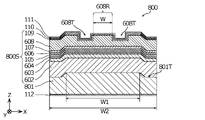

Classifications
-
- H—ELECTRICITY
- H01—ELECTRIC ELEMENTS
- H01S—DEVICES USING THE PROCESS OF LIGHT AMPLIFICATION BY STIMULATED EMISSION OF RADIATION [LASER] TO AMPLIFY OR GENERATE LIGHT; DEVICES USING STIMULATED EMISSION OF ELECTROMAGNETIC RADIATION IN WAVE RANGES OTHER THAN OPTICAL
- H01S5/00—Semiconductor lasers
- H01S5/20—Structure or shape of the semiconductor body to guide the optical wave ; Confining structures perpendicular to the optical axis, e.g. index or gain guiding, stripe geometry, broad area lasers, gain tailoring, transverse or lateral reflectors, special cladding structures, MQW barrier reflection layers
-
- H—ELECTRICITY
- H01—ELECTRIC ELEMENTS
- H01S—DEVICES USING THE PROCESS OF LIGHT AMPLIFICATION BY STIMULATED EMISSION OF RADIATION [LASER] TO AMPLIFY OR GENERATE LIGHT; DEVICES USING STIMULATED EMISSION OF ELECTROMAGNETIC RADIATION IN WAVE RANGES OTHER THAN OPTICAL
- H01S5/00—Semiconductor lasers
- H01S5/30—Structure or shape of the active region; Materials used for the active region
- H01S5/3013—AIIIBV compounds
-
- H—ELECTRICITY
- H01—ELECTRIC ELEMENTS
- H01S—DEVICES USING THE PROCESS OF LIGHT AMPLIFICATION BY STIMULATED EMISSION OF RADIATION [LASER] TO AMPLIFY OR GENERATE LIGHT; DEVICES USING STIMULATED EMISSION OF ELECTROMAGNETIC RADIATION IN WAVE RANGES OTHER THAN OPTICAL
- H01S5/00—Semiconductor lasers
- H01S5/04—Processes or apparatus for excitation, e.g. pumping, e.g. by electron beams
- H01S5/042—Electrical excitation ; Circuits therefor
- H01S5/0425—Electrodes, e.g. characterised by the structure
- H01S5/04252—Electrodes, e.g. characterised by the structure characterised by the material
-
- H—ELECTRICITY
- H01—ELECTRIC ELEMENTS
- H01S—DEVICES USING THE PROCESS OF LIGHT AMPLIFICATION BY STIMULATED EMISSION OF RADIATION [LASER] TO AMPLIFY OR GENERATE LIGHT; DEVICES USING STIMULATED EMISSION OF ELECTROMAGNETIC RADIATION IN WAVE RANGES OTHER THAN OPTICAL
- H01S5/00—Semiconductor lasers
- H01S5/20—Structure or shape of the semiconductor body to guide the optical wave ; Confining structures perpendicular to the optical axis, e.g. index or gain guiding, stripe geometry, broad area lasers, gain tailoring, transverse or lateral reflectors, special cladding structures, MQW barrier reflection layers
- H01S5/2004—Confining in the direction perpendicular to the layer structure
- H01S5/2009—Confining in the direction perpendicular to the layer structure by using electron barrier layers
-
- H—ELECTRICITY
- H01—ELECTRIC ELEMENTS
- H01S—DEVICES USING THE PROCESS OF LIGHT AMPLIFICATION BY STIMULATED EMISSION OF RADIATION [LASER] TO AMPLIFY OR GENERATE LIGHT; DEVICES USING STIMULATED EMISSION OF ELECTROMAGNETIC RADIATION IN WAVE RANGES OTHER THAN OPTICAL
- H01S5/00—Semiconductor lasers
- H01S5/20—Structure or shape of the semiconductor body to guide the optical wave ; Confining structures perpendicular to the optical axis, e.g. index or gain guiding, stripe geometry, broad area lasers, gain tailoring, transverse or lateral reflectors, special cladding structures, MQW barrier reflection layers
- H01S5/2004—Confining in the direction perpendicular to the layer structure
- H01S5/2018—Optical confinement, e.g. absorbing-, reflecting- or waveguide-layers
- H01S5/2031—Optical confinement, e.g. absorbing-, reflecting- or waveguide-layers characterized by special waveguide layers, e.g. asymmetric waveguide layers or defined bandgap discontinuities
-
- H—ELECTRICITY
- H01—ELECTRIC ELEMENTS
- H01S—DEVICES USING THE PROCESS OF LIGHT AMPLIFICATION BY STIMULATED EMISSION OF RADIATION [LASER] TO AMPLIFY OR GENERATE LIGHT; DEVICES USING STIMULATED EMISSION OF ELECTROMAGNETIC RADIATION IN WAVE RANGES OTHER THAN OPTICAL
- H01S5/00—Semiconductor lasers
- H01S5/30—Structure or shape of the active region; Materials used for the active region
- H01S5/32—Structure or shape of the active region; Materials used for the active region comprising PN junctions, e.g. hetero- or double- heterostructures
- H01S5/3211—Structure or shape of the active region; Materials used for the active region comprising PN junctions, e.g. hetero- or double- heterostructures characterised by special cladding layers, e.g. details on band-discontinuities
-
- H—ELECTRICITY
- H01—ELECTRIC ELEMENTS
- H01S—DEVICES USING THE PROCESS OF LIGHT AMPLIFICATION BY STIMULATED EMISSION OF RADIATION [LASER] TO AMPLIFY OR GENERATE LIGHT; DEVICES USING STIMULATED EMISSION OF ELECTROMAGNETIC RADIATION IN WAVE RANGES OTHER THAN OPTICAL
- H01S5/00—Semiconductor lasers
- H01S5/30—Structure or shape of the active region; Materials used for the active region
- H01S5/32—Structure or shape of the active region; Materials used for the active region comprising PN junctions, e.g. hetero- or double- heterostructures
- H01S5/3211—Structure or shape of the active region; Materials used for the active region comprising PN junctions, e.g. hetero- or double- heterostructures characterised by special cladding layers, e.g. details on band-discontinuities
- H01S5/3213—Structure or shape of the active region; Materials used for the active region comprising PN junctions, e.g. hetero- or double- heterostructures characterised by special cladding layers, e.g. details on band-discontinuities asymmetric clading layers
-
- H—ELECTRICITY
- H01—ELECTRIC ELEMENTS
- H01S—DEVICES USING THE PROCESS OF LIGHT AMPLIFICATION BY STIMULATED EMISSION OF RADIATION [LASER] TO AMPLIFY OR GENERATE LIGHT; DEVICES USING STIMULATED EMISSION OF ELECTROMAGNETIC RADIATION IN WAVE RANGES OTHER THAN OPTICAL
- H01S5/00—Semiconductor lasers
- H01S5/30—Structure or shape of the active region; Materials used for the active region
- H01S5/34—Structure or shape of the active region; Materials used for the active region comprising quantum well or superlattice structures, e.g. single quantum well [SQW] lasers, multiple quantum well [MQW] lasers or graded index separate confinement heterostructure [GRINSCH] lasers
- H01S5/3407—Structure or shape of the active region; Materials used for the active region comprising quantum well or superlattice structures, e.g. single quantum well [SQW] lasers, multiple quantum well [MQW] lasers or graded index separate confinement heterostructure [GRINSCH] lasers characterised by special barrier layers
-
- H—ELECTRICITY
- H01—ELECTRIC ELEMENTS
- H01S—DEVICES USING THE PROCESS OF LIGHT AMPLIFICATION BY STIMULATED EMISSION OF RADIATION [LASER] TO AMPLIFY OR GENERATE LIGHT; DEVICES USING STIMULATED EMISSION OF ELECTROMAGNETIC RADIATION IN WAVE RANGES OTHER THAN OPTICAL
- H01S5/00—Semiconductor lasers
- H01S5/30—Structure or shape of the active region; Materials used for the active region
- H01S5/34—Structure or shape of the active region; Materials used for the active region comprising quantum well or superlattice structures, e.g. single quantum well [SQW] lasers, multiple quantum well [MQW] lasers or graded index separate confinement heterostructure [GRINSCH] lasers
- H01S5/343—Structure or shape of the active region; Materials used for the active region comprising quantum well or superlattice structures, e.g. single quantum well [SQW] lasers, multiple quantum well [MQW] lasers or graded index separate confinement heterostructure [GRINSCH] lasers in AIIIBV compounds, e.g. AlGaAs-laser, InP-based laser
- H01S5/34333—Structure or shape of the active region; Materials used for the active region comprising quantum well or superlattice structures, e.g. single quantum well [SQW] lasers, multiple quantum well [MQW] lasers or graded index separate confinement heterostructure [GRINSCH] lasers in AIIIBV compounds, e.g. AlGaAs-laser, InP-based laser with a well layer based on Ga(In)N or Ga(In)P, e.g. blue laser
-
- H—ELECTRICITY
- H01—ELECTRIC ELEMENTS
- H01S—DEVICES USING THE PROCESS OF LIGHT AMPLIFICATION BY STIMULATED EMISSION OF RADIATION [LASER] TO AMPLIFY OR GENERATE LIGHT; DEVICES USING STIMULATED EMISSION OF ELECTROMAGNETIC RADIATION IN WAVE RANGES OTHER THAN OPTICAL
- H01S5/00—Semiconductor lasers
- H01S5/30—Structure or shape of the active region; Materials used for the active region
- H01S5/34—Structure or shape of the active region; Materials used for the active region comprising quantum well or superlattice structures, e.g. single quantum well [SQW] lasers, multiple quantum well [MQW] lasers or graded index separate confinement heterostructure [GRINSCH] lasers
- H01S5/343—Structure or shape of the active region; Materials used for the active region comprising quantum well or superlattice structures, e.g. single quantum well [SQW] lasers, multiple quantum well [MQW] lasers or graded index separate confinement heterostructure [GRINSCH] lasers in AIIIBV compounds, e.g. AlGaAs-laser, InP-based laser
- H01S5/34346—Structure or shape of the active region; Materials used for the active region comprising quantum well or superlattice structures, e.g. single quantum well [SQW] lasers, multiple quantum well [MQW] lasers or graded index separate confinement heterostructure [GRINSCH] lasers in AIIIBV compounds, e.g. AlGaAs-laser, InP-based laser characterised by the materials of the barrier layers
-
- H—ELECTRICITY
- H01—ELECTRIC ELEMENTS
- H01S—DEVICES USING THE PROCESS OF LIGHT AMPLIFICATION BY STIMULATED EMISSION OF RADIATION [LASER] TO AMPLIFY OR GENERATE LIGHT; DEVICES USING STIMULATED EMISSION OF ELECTROMAGNETIC RADIATION IN WAVE RANGES OTHER THAN OPTICAL
- H01S5/00—Semiconductor lasers
- H01S5/20—Structure or shape of the semiconductor body to guide the optical wave ; Confining structures perpendicular to the optical axis, e.g. index or gain guiding, stripe geometry, broad area lasers, gain tailoring, transverse or lateral reflectors, special cladding structures, MQW barrier reflection layers
- H01S5/22—Structure or shape of the semiconductor body to guide the optical wave ; Confining structures perpendicular to the optical axis, e.g. index or gain guiding, stripe geometry, broad area lasers, gain tailoring, transverse or lateral reflectors, special cladding structures, MQW barrier reflection layers having a ridge or stripe structure
Definitions
- the present disclosure relates to a nitride-based semiconductor light-emitting device.
- nitride-based semiconductor light-emitting devices that emit blue light are known, but there is a demand for high-output nitride-based semiconductor light-emitting devices that emit ultraviolet light with a shorter wavelength (for example, Patent Document 1, etc.). reference).
- a nitride-based semiconductor light-emitting device can realize a watt-class ultraviolet laser light source, it can be used as a light source for exposure, a light source for processing, and the like.
- an active layer having a quantum well structure having an AlGaN layer as a barrier layer is used.
- the bandgap energy of the barrier layer it is necessary to increase the bandgap energy of the barrier layer.
- the Al composition ratio of the barrier layer is increased in order to increase the bandgap energy of the barrier layer, the refractive index of the barrier layer is lowered. Therefore, it is necessary to make the refractive index of the clad layer for confining the ultraviolet light in the active layer sufficiently lower than that of the barrier layer.
- the Al composition ratio must be increased in order to lower the refractive index of the clad layer.
- a clad layer made of AlGaN having such a large Al composition ratio is crystal-grown on, for example, a substrate made of GaN, tensile strain of the clad layer with respect to the substrate increases. Therefore, when a cladding layer, an active layer, and the like are crystal-grown on a wafer made of GaN in order to manufacture a nitride-based semiconductor light-emitting device, the wafer tends to crack due to tensile strain caused by the AlGaN layer. In order to suppress such cracking of the wafer, it is conceivable to reduce the distortion of the clad layer with respect to the substrate by reducing the film thickness of the clad layer made of AlGaN.
- the P-type cladding layer made of P-type AlGaN with a high Al composition ratio has a high electrical resistance, it is set to be thinner and have a higher impurity concentration than the N-type cladding layer.
- Such a P-type clad layer has a higher refractive index than the N-type clad layer 102 . Therefore, the light is biased toward the P-type clad layer from the active layer. Therefore, the light confinement coefficient to the active layer is lowered. Along with this, the thermal saturation level of the optical output is lowered. Therefore, it becomes difficult to realize a high-power nitride-based semiconductor light-emitting device.
- An object of the present disclosure is to solve such problems, and to provide a nitride-based semiconductor light-emitting device capable of reducing the strain in the semiconductor laminate and increasing the light confinement factor to the active layer.
- one aspect of the nitride-based semiconductor light-emitting device includes an N-type cladding layer, an N-side first guide layer disposed above the N-type cladding layer, and the N-type cladding layer.
- an N-side second guide layer disposed above the N-side first guide layer; an active layer disposed above the N-side second guide layer and having a well layer and a barrier layer; and an active layer disposed above the active layer.
- the bandgap energy of the barrier layer is greater than the bandgap energy of the N-side second guide layer
- the bandgap energy of the N-side second guide layer is greater than the bandgap energy of the N-side second guide layer.
- the bandgap energy of the N-side first guide layer is smaller than the bandgap energy of the N-type cladding layer, the N-type cladding layer, the N-side first guide layer, the The N-side second guide layer, the barrier layer, and the P-type cladding layer are made of a nitride-based semiconductor containing Al.
- Another aspect of the nitride-based semiconductor light emitting device includes an N-type clad layer, an N-side guide layer arranged above the N-type clad layer, and an N-side guide layer arranged above the N-side guide layer. , an active layer including a well layer and a barrier layer, and a P-type clad layer disposed above the active layer, wherein the bandgap energy of the barrier layer is larger than the average bandgap energy of the N-side guide layer.
- the bandgap energy of the N-type cladding layer is greater than the average bandgap energy of the N-side guide layer, and the bandgap energy at the lower end of the N-side guide layer is greater than the bandgap energy at the upper end
- the N-type cladding layer, the N-side guide layer, the barrier layer, and the P-type cladding layer are made of a nitride-based semiconductor containing Al.
- a nitride-based semiconductor light-emitting device capable of reducing strain in the semiconductor laminate and increasing the light confinement coefficient to the active layer.
- FIG. 1 is a schematic plan view showing the overall configuration of a nitride-based semiconductor light-emitting device according to Embodiment 1.
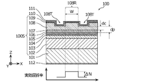
- FIG. 2A is a schematic cross-sectional view showing the overall configuration of the nitride-based semiconductor light-emitting device according to Embodiment 1.
- FIG. 2B is a schematic cross-sectional view showing the configuration of an active layer included in the nitride-based semiconductor light-emitting device according to Embodiment 1.
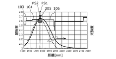
- FIG. FIG. 3 is a schematic diagram showing an overview of the light intensity distribution in the stacking direction of the nitride-based semiconductor light-emitting device according to Embodiment 1.
- FIG. 4 is a graph showing coordinates of positions in the stacking direction of the nitride-based semiconductor light-emitting device according to the first embodiment.
- FIG. 5 is a graph schematically showing the bandgap energy distribution and the light intensity distribution in the stacking direction of the semiconductor stack according to Comparative Example 1.
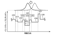
- FIG. 6 is a graph schematically showing bandgap energy distribution and light intensity distribution in the lamination direction of the semiconductor laminate according to the first embodiment.
- FIG. 7 is a graph schematically showing the bandgap energy distribution and the light intensity distribution of the semiconductor laminate according to the modification of the first embodiment.
- 8 is a graph showing a refractive index distribution and a light intensity distribution of a semiconductor laminate according to Comparative Example 2.
- FIG. 9 is a graph showing a refractive index distribution and a light intensity distribution of the semiconductor laminate according to Embodiment 1.
- FIG. FIG. 10 is a table showing the relationship between the Al composition ratio of each guide layer and the characteristics of the nitride-based semiconductor light-emitting device.
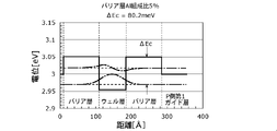
- FIG. 11 is a graph showing the relationship between the distribution of conduction band potential energy in the vicinity of the active layer and the wave function of electrons when the Al composition ratio of each barrier layer is 0.02.
- FIG. 12 is a graph showing the relationship between the distribution of conduction band potential energy in the vicinity of the active layer and the electron wave function when the Al composition ratio of each barrier layer is 0.05.
- FIG. 13 is a graph showing the relationship between the Al composition ratio of each barrier layer and the band offset ⁇ Ec.
- FIG. 14 is a graph showing the relationship between the thickness of the N-type cladding layer 102 of the nitride-based semiconductor light emitting device according to Embodiment 1 and the waveguide loss.
- FIG. 15 is a graph showing the relationship between the film thickness of the N-type cladding layer 102 of the nitride-based semiconductor light emitting device according to Embodiment 1 and the light confinement factor.
- FIG. 16 is a schematic side view showing warping of the base material and the semiconductor laminate that occur when the semiconductor laminate is laminated on the base material of the substrate according to the first embodiment.
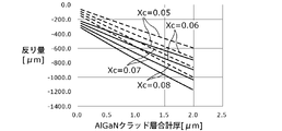
- FIG. 17 is a graph showing the amount of warpage of the base material and the semiconductor laminate that occur when the semiconductor laminate is laminated on the base material of the substrate according to the first embodiment.
- FIG. 18 is a first graph showing the relationship between each guide layer according to Embodiment 1 and the waveguide loss obtained by simulation.
- FIG. 19 is a second graph showing the relationship between each guide layer according to Embodiment 1 and the waveguide loss obtained by simulation.
- FIG. 20 is a third graph showing the relationship between each guide layer according to Embodiment 1 and the waveguide loss obtained by simulation.
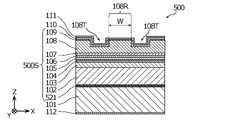
- 21A is a schematic cross-sectional view showing the overall configuration of a nitride-based semiconductor light-emitting device according to Embodiment 2.
- FIG. 21B is a schematic cross-sectional view showing the configuration of an active layer included in the nitride-based semiconductor light-emitting device according to Embodiment 2.
- FIG. 22 is a graph schematically showing bandgap energy distribution and light intensity distribution in the stacking direction of the semiconductor stack according to the second embodiment.
- FIG. 23 is a schematic cross-sectional view showing the overall configuration of a nitride-based semiconductor light-emitting device according to Embodiment 3.
- FIG. 24 is a schematic cross-sectional view showing the overall configuration of a nitride-based semiconductor light-emitting device according to Embodiment 4.
- FIG. 25 is a schematic cross-sectional view showing the overall configuration of a nitride-based semiconductor light-emitting device according to Embodiment 5.
- FIG. 23 is a schematic cross-sectional view showing the overall configuration of a nitride-based semiconductor light-emitting device according to Embodiment 3.
- FIG. 24 is a schematic cross-sectional view showing the overall configuration of a nitride-based semiconductor light-emitting device according to Embodiment 4.
- FIG. 25 is a schematic
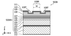
- FIG. 26 is a schematic cross-sectional view showing the overall configuration of a nitride-based semiconductor light-emitting device according to Modification 1 of Embodiment 5.
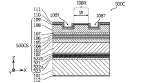
- FIG. FIG. 27 is a schematic cross-sectional view showing the overall configuration of a nitride-based semiconductor light-emitting device according to Modification 2 of Embodiment 5.
- FIG. 28 is a schematic cross-sectional view showing the overall configuration of a nitride-based semiconductor light-emitting device according to Modification 3 of Embodiment 5.
- FIG. 29 is a schematic cross-sectional view showing the overall configuration of a nitride-based semiconductor light-emitting device according to Embodiment 6.
- FIG. 30 is a schematic cross-sectional view showing the overall configuration of a nitride-based semiconductor light-emitting device according to Embodiment 7.
- FIG. 31 is a schematic cross-sectional view showing the overall configuration of a nitride-based semiconductor light-emitting device according to Embodiment 8.
- FIG. 32 is a schematic cross-sectional view showing the overall configuration of a nitride-based semiconductor light-emitting device according to Embodiment 9.
- each figure is a schematic diagram and is not necessarily strictly illustrated. Therefore, the scales and the like are not always the same in each drawing.
- symbol is attached
- the terms “upper” and “lower” do not refer to the upward direction (vertically upward) and the downward direction (vertically downward) in absolute spatial recognition, but are based on the stacking order in the stacking structure. It is used as a term defined by a relative positional relationship. Also, the terms “above” and “below” are used not only when two components are spaced apart from each other and there is another component between the two components, but also when two components are spaced apart from each other. It also applies when they are arranged in contact with each other.
- Embodiment 1 A nitride-based semiconductor light-emitting device according to Embodiment 1 will be described.
- FIGS. 1, 2A and 2B are a schematic plan view and a cross-sectional view, respectively, showing the overall configuration of a nitride-based semiconductor light-emitting device 100 according to this embodiment.
- FIG. 2A shows a cross-section along line II-II of FIG.
- FIG. 2B is a schematic cross-sectional view showing the configuration of the active layer 105 included in the nitride-based semiconductor light emitting device 100 according to this embodiment.
- Each figure shows an X-axis, a Y-axis, and a Z-axis that are orthogonal to each other.
- the X, Y, and Z axes are a right-handed Cartesian coordinate system.
- the stacking direction of the nitride-based semiconductor light emitting device 100 is parallel to the Z-axis direction, and the main emission direction of light (laser light) is parallel to the Y-axis direction.
- the nitride-based semiconductor light-emitting device 100 includes a semiconductor laminate 100S including nitride-based semiconductor layers. Light is emitted from the end face 100F (see FIG. 1).
- the nitride-based semiconductor light-emitting device 100 is a semiconductor laser device having two facets 100F and 100R forming a resonator.
- the end surface 100F is a front end surface that emits laser light
- the end surface 100R is a rear end surface having a higher reflectance than the end surface 100F.
- the reflectances of the end faces 100F and 100R are 16% and 95%, respectively.
- the nitride-based semiconductor light emitting device 100 has a waveguide formed between the facet 100F and the facet 100R.
- the cavity length of nitride-based semiconductor light-emitting device 100 according to the present embodiment (that is, the distance between facet 100F and facet 100R) is about 1200 ⁇ m.
- the nitride-based semiconductor light emitting device 100 emits ultraviolet light having a peak wavelength in the 375 nm band, for example.
- the nitride-based semiconductor light emitting device 100 includes a substrate 101, a semiconductor laminate 100S, a current blocking layer 110, a P-side electrode 111, and an N-side electrode 112.
- the semiconductor laminate 100S includes an N-type cladding layer 102, an N-side first guide layer 103, an N-side second guide layer 104, an active layer 105, a P-side first guide layer 106, and an electron barrier layer 107. , a P-type cladding layer 108 and a contact layer 109 .
- the substrate 101 is a plate-like member that serves as a base for the nitride-based semiconductor light emitting device 100 .
- substrate 101 is an N-type GaN substrate.
- the substrate 101 is doped with, for example, Si at a concentration of 1 ⁇ 10 18 cm ⁇ 3 as an impurity.
- the N-type clad layer 102 is an example of a clad layer arranged above the substrate 101 .
- the N-type cladding layer 102 is a layer having a lower refractive index and a higher bandgap energy than the active layer 105 .
- the N-type cladding layer 102 is an N-type Al 0.065 Ga 0.935 N layer with a thickness of 540 nm.
- the N-type cladding layer 102 is doped with Si at a concentration of 5 ⁇ 10 17 cm ⁇ 3 as an impurity.
- the N-type clad layer 102 is laminated above the substrate 101 made of GaN.
- the lattice constant of the N-type cladding layer 102 becomes equal to the lattice constant of the substrate 101, and at least Al, Ga, and In
- the strain of each layer, the band structure, and the refractive index can be controlled by adjusting the composition of each layer. Structural control of the nitride-based semiconductor light emitting device 100 is facilitated. Therefore, desired characteristics can be easily obtained in the nitride-based semiconductor light emitting device 100 .
- the N-side first guide layer 103 is an example of an N-side guide layer arranged above the N-type cladding layer 102 .
- the bandgap energy of the N-side first guide layer 103 is smaller than the bandgap energy of the N-type cladding layer 102 . That is, the N-side first guide layer 103 has a higher refractive index than the N-type cladding layer 102 .
- the N-side first guide layer 103 is made of Al Xn1 Ga 1-Xn1 N (0 ⁇ Xn1 ⁇ 1).
- the N-side first guide layer 103 is an N-type Al 0.03 Ga 0.97 N layer with a thickness of 100 nm.
- the N-side first guide layer 103 is doped with Si at a concentration of 5 ⁇ 10 17 cm ⁇ 3 as an impurity.
- the N-side second guide layer 104 is an example of an N-side guide layer arranged above the N-side first guide layer 103 .
- the N-side second guide layer 104 has a higher refractive index and a lower bandgap energy than the N-type cladding layer 102 .
- the bandgap energy of the N-side second guide layer 104 is smaller than the bandgap energy of the N-side first guide layer 103 . That is, the N-side second guide layer 104 has a higher refractive index than the N-side first guide layer 103 .
- the N-side second guide layer 104 is made of Al Xn2 Ga 1-Xn2 N (0 ⁇ Xn2 ⁇ 1).
- the N-side second guide layer 104 is an undoped Al 0.02 Ga 0.98 N layer with a thickness of 120 nm.
- the impurity concentration of the N-side second guide layer 104 is lower than the impurity concentration of the N-side first guide layer 103 .
- the N-side first guide layer 103 and the N-side second guide layer 104 are used. It is effective to dope an impurity into each guide layer to reduce the potential of the valence band of each guide layer.
- an increase in waveguide loss caused by impurities can be suppressed.
- the N-side second guide layer 104 is not doped with an impurity, but the N-side second guide layer 104 may be doped with an impurity.
- the resistance of the N-side second guide layer 104 is lowered, so electrons easily flow from the substrate 101 to the active layer 105, and the hole current component leaking from the active layer 105 to the substrate 101 can be reduced.
- the active layer 105 is a light-emitting layer arranged above the N-side second guide layer 104 and having a quantum well structure.
- the active layer 105 has a well layer 105b and barrier layers 105a and 105c, as shown in FIG. 2B.
- the barrier layer 105a is a layer arranged above the N-side second guide layer 104 and functioning as a barrier for the quantum well structure.
- the barrier layer 105a is made of Al b Ga 1-b N (0 ⁇ b ⁇ 1).
- the barrier layer 105a is an undoped Al 0.05 Ga 0.95 N layer with a thickness of 12 nm.
- the well layer 105b is a layer arranged above the barrier layer 105a and functioning as a well of the quantum well structure.
- the well layer 105b is arranged between the barrier layers 105a and 105c.
- the well layer 105b is an undoped In 0.01 Ga 0.99 N layer with a thickness of 7.5 nm.
- the barrier layer 105c is a layer arranged above the well layer 105b and functioning as a barrier for the quantum well structure.
- the barrier layer 105c is made of Al b Ga 1-b N (0 ⁇ b ⁇ 1).
- the barrier layer 105c is an undoped Al 0.05 Ga 0.95 N layer with a thickness of 10 nm.
- the P-side first guide layer 106 is an optical guide layer arranged above the active layer 105 .
- the P-side first guide layer 106 is arranged between the active layer 105 and the P-type cladding layer 108 .
- the bandgap energy of the P-side first guide layer 106 is smaller than the bandgap energy of the P-type cladding layer 108 .
- the refractive index of the P-side first guide layer 106 is higher than the refractive index of the P-type cladding layer 108 .
- the P-side first guide layer 106 is a P-type Al 0.02 Ga 0.98 N layer with a thickness of 200 nm.
- the P-side first guide layer 106 is doped with Mg at a concentration of 1 ⁇ 10 18 cm ⁇ 3 as an impurity.
- the electron barrier layer 107 is a nitride-based semiconductor layer arranged above the active layer 105 .
- the electron barrier layer 107 is arranged between the P-side first guide layer 106 and the P-type cladding layer 108 .
- the electron barrier layer 107 is an Al Xd Ga 1-Xd N layer with a thickness of 1 nm or more and 10 nm or less, and the Al composition ratio Xd is 0.2 or more.
- the impurity concentration with which the electron barrier layer 107 is doped may be 1 ⁇ 10 19 cm ⁇ 3 or more.
- the electron barrier layer 107 has a thin film thickness of 10 nm or less, the influence on the light intensity distribution can be reduced.
- the electron barrier layer 107 is a P-type Al 0.36 Ga 0.64 N layer with a thickness of 5 nm.
- the electron barrier layer 107 is doped with Mg at a concentration of 1 ⁇ 10 19 cm ⁇ 3 as an impurity. Since the electron barrier layer 107 can suppress leakage of electrons from the active layer 105 to the P-type clad layer 108, the light conversion efficiency of the nitride-based semiconductor light emitting device 100 can be enhanced.
- the P-type clad layer 108 is a P-type clad layer arranged above the active layer 105 .
- the P-type clad layer 108 is arranged between the electron barrier layer 107 and the contact layer 109 .
- the bandgap energy of the P-type clad layer 108 is greater than the bandgap energy of the barrier layers 105 a and 105 c of the active layer 105 and the P-side first guide layer 106 .
- the refractive index of the P-type clad layer 108 is smaller than the refractive indices of the barrier layers 105a and 105c of the active layer 105 and the P-side first guide layer 106.
- the P-type clad layer 108 is a P-type Al 0.065 Ga 0.935 N layer with a thickness of 450 nm.
- the P-type clad layer 108 is doped with Mg as an impurity.
- the P-type cladding layer 108 is located below the vertical center of the P-type cladding layer 108 (that is, on the side closer to the active layer 105), and has an impurity concentration lower than that of other regions in the P-type cladding layer 108. Contains concentration regions.
- the P-type cladding layer 108 includes a P-type Al 0.065 Ga 0.935 N layer with a thickness of 150 nm doped with Mg at a concentration of 2 ⁇ 10 18 cm ⁇ 3 disposed below and a P-type Al 0.065 Ga 0.935 N layer disposed below. and a P-type Al 0.065 Ga 0.935 N layer with a thickness of 300 nm doped with Mg at a concentration of 1 ⁇ 10 19 cm ⁇ 3 disposed on the side (that is, farther from the active layer 105).
- free carrier loss caused by impurities in the P-type cladding layer 108 can be reduced, thereby reducing waveguide loss.
- a ridge 108R is formed in the P-type cladding layer 108 of the nitride-based semiconductor light emitting device 100.
- the P-type cladding layer 108 is formed with two grooves 108T arranged along the ridge 108R and extending in the Y-axis direction.
- the ridge width W is approximately 30 ⁇ m.
- the distance between the lower end of the ridge 108R (that is, the bottom of the trench 108T) and the active layer 105 is dp.
- the film thickness of the P-type clad layer 108 at the lower end of the ridge 108R (that is, the distance between the lower end of the ridge 108R and the interface between the P-type clad layer 108 and the electron barrier layer 107) is dc.
- the contact layer 109 is a layer arranged above the P-type cladding layer 108 and in ohmic contact with the P-side electrode 111 .
- the contact layer 109 is a P-type GaN layer with a thickness of 100 nm.
- the contact layer 109 is doped with Mg at a concentration of 1 ⁇ 10 20 cm ⁇ 3 as an impurity.
- the N-type cladding layer 102, the N-side first guide layer 103, the N-side second guide layer 104, the barrier layers 105a and 105c, the P-side first The guide layer 106, the electron barrier layer 107, and the P-type cladding layer 108 are made of a nitride semiconductor containing Al.
- the current blocking layer 110 is an insulating layer arranged above the P-type cladding layer 108 and having transparency to light from the active layer 105 .
- the current blocking layer 110 is arranged in a region of the upper surface of the P-type cladding layer 108 other than the upper surface of the ridge 108R.
- the current blocking layer 110 is a SiO2 layer.
- the P-side electrode 111 is a conductive layer arranged above the contact layer 109 .
- the P-side electrode 111 is arranged above the contact layer 109 and the current blocking layer 110 .
- the P-side electrode 111 is, for example, a single layer film or a multilayer film made of at least one of Cr, Ti, Ni, Pd, Pt and Au.
- the N-side electrode 112 is a conductive layer arranged below the substrate 101 (that is, on the main surface of the substrate 101 opposite to the main surface on which the semiconductor laminate 100S is arranged).
- the N-side electrode 112 is, for example, a single layer film or a multilayer film made of at least one of Cr, Ti, Ni, Pd, Pt and Au.
- the nitride-based semiconductor light emitting device 100 has an effective refractive index difference ⁇ N between the portion below the ridge 108R and the portion below the groove 108T, as shown in FIG. 2A. occurs. Thereby, the light generated in the portion of the active layer 105 below the ridge 108R can be confined in the horizontal direction (that is, in the X-axis direction).
- FIG. 3 is a schematic diagram showing an overview of the light intensity distribution in the stacking direction of the nitride-based semiconductor light emitting device 100 according to this embodiment.
- FIG. 3 shows a schematic cross-sectional view of the nitride-based semiconductor light emitting device 100 and a graph showing an overview of the light intensity distribution in the stacking direction at positions corresponding to the ridges 108R and the grooves 108T.
- a nitride-based semiconductor light-emitting device In a nitride-based semiconductor light-emitting device, light is generated in the active layer, but the light intensity distribution in the lamination direction depends on the lamination structure, and the peak of the light intensity distribution is not necessarily located in the active layer.
- the laminated structure of the nitride-based semiconductor light-emitting device 100 according to the present embodiment differs between the portion below the ridge 108R and the portion below the groove 108T, the light intensity distribution is also different in the portion below the ridge 108R. and the portion below the groove 108T. As shown in FIG.
- FIG. 4 is a graph showing coordinates of positions in the stacking direction of the nitride-based semiconductor light-emitting device 100 according to the present embodiment. As shown in FIG.
- the coordinates of the position of the end face of the active layer 105 on the N side of the well layer 105b, that is, the end face of the well layer 105b closer to the N-type cladding layer 102 in the stacking direction is set to zero, and downward ( The direction toward the N-type cladding layer 102) is the negative direction of the coordinates, and the upward direction (the direction toward the P-type cladding layer 108) is the positive direction of the coordinates.
- the absolute value of the difference between the positions PS1 and PS2 is defined as the peak position difference ⁇ P.
- FIGS. 5 to 7 are graphs schematically showing the bandgap energy distribution and the light intensity distribution in the stacking direction of the semiconductor stacks according to Comparative Example 1 and the present embodiment, respectively.
- FIG. 7 is a graph schematically showing the bandgap energy distribution and the light intensity distribution of the semiconductor laminate according to the modification of the present embodiment.
- the semiconductor laminate according to Comparative Example 1 differs from the semiconductor laminate 100S according to the present embodiment in the configurations of the N-side guide layer 993, the active layer 995, and the P-side guide layer 996.
- the active layer 995 also has barrier layers 995a and 995c and a well layer 995b.
- Each guide layer according to Comparative Example 1 has a higher bandgap energy than the barrier layers 995a and 995c. That is, each guide layer according to Comparative Example 1 has a smaller refractive index than the barrier layers 995a and 995c.
- each clad layer made of AlGaN with a high Al composition ratio in order to emit ultraviolet light.
- the tensile strain of each clad layer made of AlGaN with respect to the substrate 101 made of GaN increases, and the base material of the substrate 101 is likely to crack during the manufacture of the nitride-based semiconductor light-emitting device.
- the tensile strain is suppressed by reducing the film thickness of each clad layer.
- the P-type cladding layer 108 made of P-type AlGaN with a high Al composition ratio has a high electrical resistance, it is set to be thinner and have a higher impurity concentration than the N-type cladding layer 102 .
- Such a P-type clad layer 108 has a higher refractive index than the N-type clad layer 102 .
- the bandgap energy of the barrier layers 105a and 105c is higher than the bandgap energy of the N-side second guide layer 104.
- the barrier layers 105a and 105c are made of AlbGa1 - bN (0 ⁇ b ⁇ 1), and the N-side second guide layer 104 is made of AlXn2Ga1 -Xn2N (0 ⁇ Xn2 ⁇ 1). , then b>Xn2.
- the bandgap energy of the N-side second guide layer 104 is smaller than the bandgap energy of the N-side first guide layer 103, and the bandgap energy of the N-side first guide layer 103 is less than the bandgap energy of the N-type cladding layer 102. less than energy. That is, when the N-side first guide layer 103 is made of Al Xn1 Ga 1-Xn1 N (0 ⁇ Xn1 ⁇ 1) and the N-type cladding layer 102 is made of Al Xnc Ga 1-Xnc N (0 ⁇ Xnc ⁇ 1), Xn2 ⁇ Xn1, Xn1 ⁇ Xnc.
- the bandgap energy of the N-side second guide layer 104 which is the guide layer closer to the barrier layer 105a, is smaller than the bandgap energy of the barrier layer 105a. That is, the N-side second guide layer 104 has a higher refractive index than the barrier layer 105a. Also, the refractive index of the N-side second guide layer 104 closer to the active layer 105 than the N-side first guide layer 103 is higher than the refractive index of the N-side first guide layer 103 . Since the semiconductor laminate 100S has such a refractive index distribution, the light intensity distribution can be shifted toward the N-side second guide layer 104 as compared with the semiconductor laminate according to Comparative Example 1.
- N-side second guide layer 104 As shown in FIG. 6, it is possible to bring the peak position of the light intensity distribution closer to the active layer 105 than in the semiconductor laminate according to Comparative Example 1. . Furthermore, since the active layer 105 is not doped with impurities, the waveguide loss caused by light absorption by impurities can be reduced by locating the peak position of the light intensity distribution in the region near the active layer 105.
- the N-side first guide layer 103 and the N-side second guide layer 104 may be collectively referred to as one N-side guide layer.
- the bandgap energy at the lower end of the N-side guide layer (that is, the bandgap energy of the N-side first guide layer 103) is the bandgap energy at the upper end (that is, the N-side second guide layer 104 bandgap energy).
- the bandgap energy of the barrier layers 105a and 105c is larger than the average bandgap energy of the N-side guide layers.
- the Al composition ratio of the N-side first guide layer 103 is represented by Xn1 and the Al composition ratio of the N-side second guide layer 104 is represented by Xn2, Xn1>Xn2 relationship is established. That is, the bandgap energy of the N-side second guide layer 104 is smaller than the bandgap energy of the N-side first guide layer 103 . Therefore, as described above, compared to the semiconductor laminate according to Comparative Example 1, it is possible to bring the peak position of the light intensity distribution closer to the active layer 105 more reliably.
- the N-side second guide layer 104 is thicker than the N-side first guide layer 103. It differs from the semiconductor stacked body 100S according to the embodiment, but is the same in other respects.
- the film thickness of the N-side second guide layer 104 having a larger refractive index than that of the N-side first guide layer 103 thicker than the film thickness of the N-side first guide layer 103, the light intensity in the lamination direction
- the peak position of the distribution tends to spread toward the N-type cladding layer 102 side. Therefore, the controllability of positioning the peak position of the light intensity distribution in the region near the active layer 105 can be enhanced. As a result, it is possible to prevent the peak position from being excessively biased in the direction from the active layer 105 toward the P-side first guide layer 106 .
- FIGS. 8 and 9 are graphs showing refractive index distributions and light intensity distributions of semiconductor laminates according to Comparative Example 2 and the present embodiment.
- the Al composition ratio of the N-side second guide layer 904 is 0.03, which is the same as that of the N-side first guide layer 103 and the P-side first guide layer 106.
- the N-side first guide layer 103 and the N-side second guide layer 904 of the semiconductor laminate according to Comparative Example 2 and the P-side first guide layer 106 have the same Al composition ratio. However, the impurity concentration is different. Therefore, the P-side first guide layer 106 has a higher refractive index than the N-side first guide layer 103 and the N-side second guide layer 904 . Therefore, the peak positions PS1 and PS2 of the light intensity distribution are biased in the direction from the active layer toward the P-side guide layer. Specifically, the peak position PS1 is 96.3 nm, and the peak position difference ⁇ P is 33.4 nm.
- the refractive index of the N-side second guide layer 104 is higher than the refractive index of the N-side first guide layer 103, so in the case of the semiconductor laminate according to Comparative Example 2, As a result, the peak positions PS1 and PS2 of the light intensity distribution are closer to the active layer 105. FIG. Therefore, the optical confinement factor to the active layer 105 can be increased, and the waveguide loss can be reduced. Also, both the peak positions PS1 and PS2 are brought closer to the active layer 105, and the absolute value of the difference between the positions PS1 and PS2 also becomes smaller. Specifically, the peak position PS1 is 77.1 nm, and the peak position difference ⁇ P is 32.0 nm.
- the portion below the ridge 108R and the portion below the groove 108T is set so that the effective refractive index difference ⁇ N between is relatively small.
- the effective refractive index difference ⁇ N is set by adjusting the distance dp between the current blocking layer 110 and the active layer 105 (see FIG. 2A).
- the larger the distance dp the smaller the effective refractive index difference ⁇ N.
- the effective refractive index difference ⁇ N is about 7.4 ⁇ 10 ⁇ 3 .
- the higher-order mode (that is, the higher-order transverse mode) capable of propagating through the waveguide formed by the ridge 108R is higher than when the effective refractive index difference ⁇ N is larger than 7.4 ⁇ 10 ⁇ 3 . small number.
- ⁇ N becomes smaller, the number of higher-order modes propagating through the waveguide decreases, so the proportion of each higher-order mode among all the transverse modes contained in the light emitted from the nitride-based semiconductor light-emitting device 100 increases. Therefore, the influence of the change in the optical confinement coefficient to the active layer 105 due to the increase or decrease in the number of modes and the coupling between modes becomes relatively large.
- the basic mode is the 0th order mode.
- the linearity of the optical output characteristic (so-called IL characteristic) with respect to the supplied current is degraded.
- non-linear portions (so-called kinks) occur in the graph showing the IL characteristics.
- the stability of the light output of the nitride-based semiconductor light emitting device 100 may be degraded.
- the distribution of light propagating through the waveguide is two-dimensionally distributed in regions inside and outside the ridge 108R when viewed from the normal direction of the laser facet. Since a higher-order mode has a lower effective refractive index, the light distribution tends to expand to the trench 108T in the region outside the ridge 108R and is more susceptible to the current blocking layer 110.
- FIG. Current blocking layer 110 is composed of a material with a lower refractive index than P-type cladding layer 108 in order to laterally confine light in ridge 108R.
- the peak position PS2 of the light distribution in the stacking direction at the trench 108T in the region outside the ridge 108R is influenced by the current blocking layer 110, and the peak position PS1 of the light distribution in the stacking direction at the ridge 108R is stacked.
- the direction bias toward the substrate 101 tends to increase.
- the stacking direction peak position in the groove 108T of the waveguide mode is closest to the substrate 101 with respect to the other waveguide mode light, and the average value of the peak positions in the stacking direction light distribution in the horizontal direction is It comes to be approximated by the stacking direction peak position.
- the effective refractive index difference ⁇ N is reduced in order to reduce the horizontal divergence angle of emitted light.
- the nitride-based semiconductor light-emitting device 100 includes the N-side first guide layer 103, the N-side second guide layer 104, and the P-side first guide layer 106 having the configurations as described above. Therefore, in both the portion below the ridge 108R and the portion below the trench 108T, the peak of the light intensity distribution can be brought closer to the active layer 105, and the positions PS1 and PS2 of the peaks of the light intensity distribution can be adjusted. can be reduced.
- the distance dp is set to a relatively large value in order to set the effective refractive index difference ⁇ N to a relatively small value.
- the distance dp is set so that the lower end of the ridge 108R (that is, the bottom of the trench 108T) is positioned below the electron barrier layer 107, the electron barrier layer 107 has a large bandgap energy, so contact Holes injected from layer 109 tend to leak from the sidewalls of ridge 108R to the outside of ridge 108R when passing through electron blocking layer 107 . As a result, holes flow below trench 108T.
- the lower end of the ridge 108R is set above the electron barrier layer 107.
- the distance dc (see FIG. 2A) from the lower end of the ridge 108R to the electron barrier layer 107 becomes too large, holes flow from the ridge 108R between the trench 108T and the electron barrier layer 107, resulting in leakage current. Become.
- the distance dc is set to a value as small as possible.
- dc should be 70 nm or less. If dc is 45 nm or less, it is possible to further reduce changes in oscillation threshold due to variations in dc.
- FIG. 10 shows the Al composition ratios of the N-side first guide layer 103, the N-side second guide layer 104, and the P-side first guide layer 106 of the nitride-based semiconductor light-emitting device 100 according to this embodiment.
- FIG. 10 is a table showing the relationship between the Al composition ratio of each guide layer and the characteristics of the nitride-based semiconductor light-emitting device.
- FIG. 10 shows the relationship between the nine Al composition ratios of Comparative Example and Composition Examples 1 to 8 and the characteristics of the nitride-based semiconductor light-emitting device obtained by simulation.
- the well thickness normalized light confinement coefficient is a value obtained by dividing the light confinement coefficient by the thickness Tw of the well layer.
- the Al composition ratio of each guide layer according to the comparative example is 0.03 (that is, 3%).
- Structural Examples 1 to 8 have different combinations of Al composition ratios.
- the Al composition ratio is selected from 0.02 (ie 2%), 0.03 (ie 3%) and 0.04 (ie 4%).
- FIG. 10 shows characteristics for three cases where the well layer thickness (well thickness Tw in FIG. 10) is 7.5 nm, 12.5 nm, and 17.5 nm.
- the bandgap energy of the N-side second guide layer 104 is preferably smaller than the bandgap energy of the N-side first guide layer 103 as in the nitride-based semiconductor light emitting device 100 according to this embodiment.
- the film thickness Tw of the well layer increases, the optical confinement coefficient, waveguide loss, peak position PS1, and peak position difference ⁇ P are improved. This is because the light intensity distribution in the stacking direction approaches the well layer by increasing the thickness of the well layer having a large refractive index.
- the film thickness Tw of the well layer may be 10 nm or more.
- the film thickness Tw of the well layer may be 20 nm or less in order to realize a quantum well active layer.
- FIG. 11 and 12 are graphs showing the relationship between the conduction band potential energy distribution near the active layer 105 and the electron wave function when the Al composition ratios of the barrier layers are 0.02 and 0.05, respectively. is.
- the horizontal axis of the graph in each figure indicates the distance from a predetermined position, and the vertical axis indicates the potential.
- the solid line indicates the conduction band potential of each layer
- the dashed line indicates the quantized energy level of electrons
- the dashed-dotted line indicates the wave function of electrons.
- FIG. 13 is a graph showing the relationship between the Al composition ratio of each barrier layer and the band offset ⁇ Ec.
- the band offset ⁇ Ec is increased by increasing the barrier layers 105a and 105c.
- the Al composition ratio of the barrier layers 105a and 105c is 0.02, which is the same as the Al composition ratio of the N-side second guide layer 104, the band offset ⁇ Ec is 31 meV.
- leakage of electrons from the barrier layer 105c cannot be sufficiently suppressed during high-power operation.
- the electron confinement effect in the well layer 105b is small. Therefore, in this embodiment, by setting the Al composition ratio of the barrier layers 105a and 105c to 0.05, as shown in FIG. It is made larger than the bandgap energy of 104. This allows the band offset ⁇ Ec to be 80.2 meV. Therefore, the electron confinement effect in the well layer 105b can be enhanced. As shown in FIG. 13, the band offset ⁇ Ec increases as the Al composition ratio of each barrier layer increases.
- the bandgap energy of the barrier layers 105 a and 105 c may be made larger than the bandgap energy of the N-side first guide layer 103 . This can further reduce the leakage of electrons from the well layer 105b.
- the energy difference between the ground quantum levels of electrons and holes formed in the well layer 105b can be increased, light in a short wavelength band such as a 375 nm wavelength band can be easily emitted in the active layer 105. can be generated to
- the barrier layers 105a and 105c are made of AlGaN
- the well layer 105b is an InGaN layer with an In composition ratio of 1% and a film thickness of 7.5 nm
- the Al composition of the barrier layers 105a and 105c is By setting the ratio to 0.04 or more, the band offset ⁇ Ec can be set to 80 meV or more. Thereby, leakage of electrons from the well layer 105b can be suppressed.
- the band offset ⁇ Ec can be set to 167 meV or more by setting the Al composition ratio of the barrier layers 105a and 105c to 0.05 or more. can do.
- the difference between the electron quantum level and the conduction band potential energy of the well layer 105b is reduced, so that the band offset ⁇ Ec can be further increased.
- FIGS. 14 and 15 are graphs showing the relationship between the thickness of the N-type cladding layer 102 of the nitride-based semiconductor light emitting device 100 according to this embodiment, and the waveguide loss and optical confinement factor, respectively.
- the graphs shown in FIGS. 14 and 15 are obtained by simulation.
- the Al composition ratios of the N-type clad layer 102 and the P-type clad layer 108 are both set to the same Al composition ratio Xc, and the Al composition ratio Xc and the film thickness of the N-type clad layer 102 are changed.
- calculating the waveguide loss and the optical confinement factor. 14 and 15 show the waveguide loss and optical confinement factor when the Al composition ratio Xc is 0.05, 0.06, 0.07, 0.08, and 0.09, respectively. It is In the nitride-based semiconductor light-emitting device 100 calculated in this simulation, a buffer layer is provided between the substrate 101 and the N-type cladding layer 102 .
- the buffer layer includes an N-type Al 0.007 Ga 0.993 N layer with a thickness of 1000 nm and an N-type In 0.05 Ga 0.95 N layer with a thickness of 150 nm which are sequentially laminated on the substrate 101 .
- the buffer layer is doped with Si at a concentration of 5 ⁇ 10 17 cm ⁇ 3 as an impurity.
- the waveguide loss tends to increase. This is probably because light leaks to the outside of the N-type cladding layer 102 (substrate 101 and buffer layer), is absorbed, or propagates in the substrate in a substrate mode.
- Such waveguide loss can be reduced by setting the film thickness of the N-type cladding layer 102 to 0.5 ⁇ m or more.
- the refractive index of each clad layer decreases and the optical confinement factor increases as shown in FIG. 15, thereby reducing the waveguide loss.
- the waveguide loss can be greatly reduced as compared with the case where the Al composition ratio is 0.05. Also, even if the Al composition ratio is greater than 0.08, the amount of reduction in waveguide loss is small compared to the waveguide loss when the Al composition ratio is 0.08. On the other hand, when the Al composition ratio is increased, the tensile strain of the semiconductor laminate 100S with respect to the substrate 101 increases. In order to suppress such an increase in tensile strain, the Al composition ratio may be 0.08.
- FIG. 16 is a schematic side view showing warpage of the base material 101M and the semiconductor stack 100S that occurs when the semiconductor stack 100S is stacked on the base material 101M of the substrate 101 according to the present embodiment.
- Base material 101M of substrate 101 shown in FIG. 16 is, for example, a GaN substrate with a diameter of 2 inches. As shown in FIG.
- the base material 101M is deformed due to tensile strain on the base material 101M caused by the AlGaN layers in the semiconductor laminate 100S. 101M and the semiconductor laminate 100S are warped.
- the upper surface of the semiconductor stacked body 100S is warped in a concave direction.
- FIG. 17 is a graph showing the amount of warpage of the base material 101M and the semiconductor stack 100S when the semiconductor stack 100S is stacked on the base material 101M of the substrate 101 according to the present embodiment.
- the horizontal axis of FIG. 17 indicates the total thickness of the N-type clad layer 102 and the P-type clad layer 108 made of Al Xc Ga 1-Xc N contained in the semiconductor laminate 100S, and the vertical axis indicates the amount of warpage.
- the amount of warp when the upper surface of the semiconductor stacked body 100S is concave that is, the depth of the concave indicated by the arrow in FIG. 16
- the warp amount that is, the height of the convex portion
- the top surface of the semiconductor stacked body 100S is convex is represented by a positive numerical value.
- FIG. 17 the simulation result of the amount of warpage when the film thickness of the N-type cladding layer 102 is changed in the nitride-based semiconductor light emitting device 100 described above is shown by a solid line. Also, FIG. 17 shows the amount of warpage when the Al composition ratio Xc of the N-type clad layer 102 and the P-type clad layer 108 is 0.05, 0.06, 0.07, and 0.08. It is In the simulation, a disk-shaped GaN substrate with a diameter of 2 inches is used as the base material 101M.
- the buffer layer includes an N-type Al 0.007 Ga 0.993 N layer with a thickness of 300 nm and an N-type In 0.05 Ga 0.95 N layer with a thickness of 150 nm which are sequentially laminated on the base material 101M. .
- the buffer layer is doped with Si at a concentration of 5 ⁇ 10 17 cm ⁇ 3 as an impurity.
- the absolute value of the amount of warpage of the base material 101M When using a GaN substrate with a diameter of 2 inches as the base material 101M, if the absolute value of the amount of warpage exceeds 800 ⁇ m, the risk of cracking the base material 101M increases. Therefore, in order to set the absolute value of the amount of warpage of the base material 101M to 700 ⁇ m or less, for example, when the Al composition ratio Xc is 0.06 or more and 0.07 or less, the total thickness of the cladding layers should be 1.1 ⁇ m or less. do it. Further, as described above with reference to FIGS.
- the film thickness of the N-type clad layer 102 is 0.5 ⁇ m or more, that is, the P-type clad layer 108 and the N-type clad layer 108 having a film thickness of 450 nm (that is, 0.45 ⁇ m).
- the total film thickness with the layer 102 is 0.95 ⁇ m or more, the waveguide loss can be suppressed and the optical confinement factor can be increased. Therefore, by setting the Al composition ratio Xc to 0.06 or more and 0.07 or less and the total thickness of the clad layers to 0.95 ⁇ m or more and 1.1 ⁇ m or less, cracking of the base material 101M is suppressed.
- a waveguide with low loss and a large optical confinement factor can be realized. Furthermore, by setting the total thickness of the clad layers to 1.0 ⁇ m or less, the absolute value of the amount of warpage of the base material 101M can be further reduced, so cracking of the base material 101M can be suppressed more reliably.
- the absolute value of the amount of warpage can be reduced. Therefore, when the buffer layer is provided, cracking of the base material 101M is suppressed, and the total thickness of the clad layers and the Al composition ratio can be increased.
- FIG. . 18 to 20 are graphs showing the relationship between each guide layer according to this embodiment and the waveguide loss obtained by simulation.
- the horizontal axis represents the film thickness Tp1 of the P-side first guide layer 106
- the vertical axis represents the waveguide loss.
- FIGS. 18 to 20 shows a graph for each case where the film thickness Tn2 of the N-side second guide layer 104 is changed from 50 nm to 200 nm by 30 nm.
- the film thickness Tn1 of the N-side first guide layer 103 is 100 nm.
- 18, 19, and 20 show the relationships when the Al composition ratio Xp1 of the P-side first guide layer 106 is 0.02, 0.03, and 0.04, respectively.
- the waveguide loss can be reduced as the film thickness Tn2 of the N-side second guide layer 104 increases. This is because, as described above, the film thickness Tn2 of the N-side second guide layer 104, which has a larger refractive index than the N-type cladding layer 102 and the N-side first guide layer 103, is increased, resulting in a change in the light intensity distribution in the stacking direction. This is because the peak position can be shifted from the P-type cladding layer 108 toward the active layer 105 . In addition, since the active layer 105 is not doped with impurities, the peak position of the light intensity distribution approaches the active layer, thereby reducing waveguide loss caused by impurities.
- the waveguide loss is can be further reduced.
- the film thickness Tp1 of the P-side first guide layer 106 When the film thickness Tp1 of the P-side first guide layer 106 is thin, the waveguide loss tends to increase. Therefore, in order to reduce waveguide loss, the film thickness Tp1 of the P-side first guide layer 106 may be 65 nm or more. Further, when the film thickness Tn2 of the N-side second guide layer 104 is 150 nm or more, the influence of the film thickness Tp1 of the P-side first guide layer 106 on the waveguide loss becomes small. That is, when the film thickness Tn2 of the N-side second guide layer 104 is 150 nm or more, the waveguide loss is substantially constant even if the film thickness Tp1 of the P-side first guide layer 106 changes. Therefore, in order to increase the flexibility of the film thickness Tp1 of the P-side first guide layer 106, the film thickness Tn2 of the N-side second guide layer 104 may be 150 nm or more.
- Embodiment 2 A nitride-based semiconductor light-emitting device according to Embodiment 2 will be described.
- the nitride-based semiconductor light-emitting device according to this embodiment differs from the nitride-based semiconductor light-emitting device 100 according to the first embodiment mainly in the configuration of the well layer.
- the nitride-based semiconductor light-emitting device according to this embodiment will be described below with reference to FIGS. 21A to 22, focusing on differences from the nitride-based semiconductor light-emitting device 100 according to the first embodiment.
- FIG. 21A is a schematic cross-sectional view showing the overall configuration of a nitride-based semiconductor light-emitting device 200 according to this embodiment.
- FIG. 21B is a schematic cross-sectional view showing the configuration of the active layer 205 included in the nitride-based semiconductor light-emitting device 200 according to this embodiment.
- FIG. 22 is a graph schematically showing the bandgap energy distribution and the light intensity distribution in the stacking direction of the semiconductor stack 200S according to this embodiment.
- a nitride-based semiconductor light-emitting device 200 includes a substrate 101, a semiconductor laminate 200S, a current blocking layer 110, a P-side electrode 111, and an N-side electrode 112.
- the semiconductor laminate 200S includes an N-type cladding layer 102, an N-side first guide layer 103, an N-side second guide layer 104, an active layer 205, a P-side first guide layer 206, and an electron barrier layer 107. , a P-type cladding layer 108 and a contact layer 109 .
- the active layer 205 has a well layer 205b and barrier layers 105a and 105c, as shown in FIG. 21B.
- the well layer 205b according to this embodiment is an undoped In 0.01 Ga 0.99 N layer with a thickness of 17.5 nm.
- the film thickness of the well layer 205b is 10 nm or more.
- the P-side first guide layer 206 is a P-type Al 0.04 Ga 0.96 N layer with a thickness of 200 nm.
- the P-side first guide layer 206 is doped with Mg at a concentration of 1 ⁇ 10 18 cm ⁇ 3 as an impurity.
- the bandgap energy of the P-type cladding layer 108 made of Al 0.065 Ga 0.935 N is greater than the bandgap energy of the P-side first guide layer 206 .
- the bandgap energy of the P-side first guide layer 206 is the same as that of the N-side first guide layer 103 made of Al 0.03 Ga 0.97 N and the N-side first guide layer 103 made of Al 0.02 Ga 0.98 N.
- the peak position of the light intensity distribution can be shifted from the P-side first guide layer 206 toward the N-side guide layer (that is, downward). Therefore, in the present embodiment, as shown in FIG. 22, the peak position of the light intensity distribution can be brought closer to the active layer 205 than in Comparative Example 1 described in the first embodiment.
- the N-type cladding layer 102 is made of Al Xnc Ga 1-Xnc N
- the N-side guide layer is made of AlGaN
- the barrier layers 105a and 105c are made of Al b Ga 1-b N.
- the P-side first guide layer 206 is made of AlGaN
- the electron barrier layer 107 is made of Al Xd Ga 1-Xd N
- the P-type cladding layer 108 is made of Al Xpc Ga 1-Xpc N
- the N-side Assuming that the average Al composition ratio of the guide layers is Xn and the average Al composition ratio of the P-side first guide layer 206 is Xp1, b>Xn, Xp1 ⁇ Xg3, Xnc>Xn, Xpc>Xp1 relationship is established. Thus, since b>Xn holds, the bandgap energies of the barrier layers 105a and 105c are larger than the average bandgap energy of the N-side guide layers.
- the barrier layers 105a and 105c have a smaller refractive index than the N-side guide layer.
- the peak position of the light intensity distribution can be shifted from the barrier layers 105a and 105c toward the N-side guide layer (that is, downward). Therefore, it is possible to bring the peak position of the light intensity distribution closer to the active layer 205 than in Comparative Example 1 described in the first embodiment.
- the effective refractive index difference ⁇ N is 4.3 ⁇ 10 ⁇ 3
- the peak position PS1 of the light intensity distribution in the stacking direction in the portion below the ridge 108R is 8.9 nm
- a nitride-based semiconductor light-emitting device 200 having a ⁇ P of 4.2 nm, a light confinement factor in the active layer 205 of 5.2%, and a waveguide loss of 3.7 cm ⁇ 1 can be realized.
- Embodiment 3 A nitride-based semiconductor light-emitting device according to Embodiment 3 will be described.
- the nitride-based semiconductor light-emitting device according to this embodiment differs from the nitride-based semiconductor light-emitting device 200 according to the second embodiment in that it includes a hole blocking layer.
- the nitride-based semiconductor light-emitting device according to the present embodiment will be described below with reference to FIG. 23, focusing on differences from the nitride-based semiconductor light-emitting device 200 according to the second embodiment.
- FIG. 23 is a schematic cross-sectional view showing the overall configuration of a nitride-based semiconductor light-emitting device 300 according to this embodiment.
- a nitride-based semiconductor light-emitting device 300 includes a substrate 101, a semiconductor laminate 300S, a current blocking layer 110, a P-side electrode 111, and an N-side electrode 112.
- the semiconductor laminate 300S includes an N-type cladding layer 102, an N-side first guide layer 103, a hole barrier layer 313, an N-side second guide layer 104, an active layer 205, and a P-side first guide layer 206. , an electron barrier layer 107 , a P-type clad layer 108 and a contact layer 109 .
- the hole blocking layer 313 is a nitride-based semiconductor layer arranged between the N-type cladding layer 102 and the active layer 205 to prevent holes from leaking from the active layer 205 to the N-type cladding layer 102 .
- the hole blocking layer 313 is arranged between the N-side first guide layer 103 and the N-side second guide layer 104 .
- the hole blocking layer 313 is an N-type Al 0.30 Ga 0.70 N layer with a thickness of 4 nm.
- the hole barrier layer 313 is doped with Si at a concentration of 5 ⁇ 10 17 cm ⁇ 3 as an impurity.
- the nitride-based semiconductor light emitting device 300 includes the N-type cladding layer 102 and the hole barrier layer 313 having a higher Al composition ratio than those of the barrier layers 105a and 105c.
- the hole barrier layer 313 may be doped with an impurity of 5 ⁇ 10 17 cm ⁇ 3 or more. Thereby, electron conductivity in the hole blocking layer 313 can be enhanced.
- the film thickness of the hole blocking layer 313 is, for example, 1 nm or more and 10 nm or less.
- the effect of the hole blocking layer 313 on the light intensity distribution can be reduced.
- the same effects as those of the nitride-based semiconductor light-emitting device 200 according to the second embodiment can be obtained.
- the effective refractive index difference ⁇ N is 4.9 ⁇ 10 ⁇ 3
- the peak position PS1 of the light intensity distribution in the stacking direction in the portion below the ridge 108R is 10.8 nm
- a nitride-based semiconductor light-emitting device 300 having a ⁇ P of 4.3 nm, a light confinement factor in the active layer 205 of 5.2%, and a waveguide loss of 5.2 cm ⁇ 1 can be realized.
- Embodiment 4 A nitride-based semiconductor light-emitting device according to Embodiment 4 will be described.
- the nitride-based semiconductor light-emitting device according to this embodiment differs from the nitride-based semiconductor light-emitting device 200 according to the second embodiment in that it includes a P-side second guide layer.
- the nitride-based semiconductor light-emitting device according to the present embodiment will be described below with reference to FIG. 24, focusing on differences from the nitride-based semiconductor light-emitting device 200 according to the second embodiment.
- FIG. 24 is a schematic cross-sectional view showing the overall configuration of a nitride-based semiconductor light-emitting device 400 according to this embodiment.
- a nitride-based semiconductor light-emitting device 400 includes a substrate 101, a semiconductor laminate 400S, a current blocking layer 110, a P-side electrode 111, and an N-side electrode 112.
- the semiconductor laminate 400S includes an N-type cladding layer 102, an N-side first guide layer 103, an N-side second guide layer 104, an active layer 205, a P-side first guide layer 406, and an electron barrier layer 107. , a P-side second guide layer 414 , a P-type cladding layer 108 and a contact layer 109 .
- the P-side second guide layer 414 is an optical guide layer arranged between the P-side first guide layer 406 and the P-type cladding layer 108 .
- the P-side second guide layer 414 is arranged between the electron barrier layer 107 and the P-type clad layer 108 .
- the P-side second guide layer 414 is a P-type Al 0.04 Ga 0.96 N layer with a thickness of 50 nm.
- the P-side second guide layer 414 is doped with Mg at a concentration of 2 ⁇ 10 18 cm ⁇ 3 as an impurity.
- the P-side first guide layer 406 is a P-type Al 0.04 Ga 0.96 N layer with a thickness of 150 nm.
- the P-side first guide layer 406 is doped with Mg at a concentration of 1 ⁇ 10 18 cm ⁇ 3 as an impurity. That is, in the present embodiment, the thickness of the P-side first guide layer 406 is thinner than the thickness of the P-side first guide layer 206 according to the second embodiment by 50 nm.
- the nitride-based semiconductor light emitting device 400 includes the P-side second guide layer 414, the thickness of the P-side first guide layer 406 is reduced by the thickness of the P-side second guide layer 414. good too.
- the nitride-based semiconductor light emitting device 400 includes the P-side second guide layer 414 arranged between the electron barrier layer 107 and the P-type cladding layer 108,
- the film thickness of the guide layer 406 is thinner than the film thickness of the P-side first guide layer 206 according to the second embodiment by the film thickness of the P-side second guide layer 414 .
- the electron barrier layer 107 is positioned closer to the well layer 205b of the active layer 205 than the electron barrier layer 107 according to the second embodiment by the thickness of the P-side second guide layer 414. placed.
- the effective refractive index difference ⁇ N is 7.4 ⁇ 10 ⁇ 3
- the peak position PS1 of the light intensity distribution in the stacking direction in the portion below the ridge 108R is 9.1 nm
- a nitride-based semiconductor light-emitting device 400 having a ⁇ P of 6.9 nm, a light confinement factor in the active layer 205 of 5.4%, and a waveguide loss of 4.5 cm ⁇ 1 can be realized.
- Embodiment 5 A nitride-based semiconductor light-emitting device according to Embodiment 5 will be described.
- the nitride-based semiconductor light-emitting device according to this embodiment differs from the nitride-based semiconductor light-emitting device 100 according to the first embodiment in that it includes a buffer layer.
- the nitride-based semiconductor light-emitting device according to the present embodiment will be described below with reference to FIG. 25, focusing on differences from the nitride-based semiconductor light-emitting device 100 according to the first embodiment.
- FIG. 25 is a schematic cross-sectional view showing the overall configuration of a nitride-based semiconductor light-emitting device 500 according to this embodiment.
- a nitride-based semiconductor light-emitting device 500 includes a substrate 101, a semiconductor laminate 500S, a current blocking layer 110, a P-side electrode 111, and an N-side electrode 112.
- the semiconductor laminate 500S includes a first buffer layer 521, an N-type cladding layer 102, an N-side first guide layer 103, an N-side second guide layer 104, an active layer 105, and a P-side first guide layer 106. , an electron barrier layer 107 , a P-type clad layer 108 and a contact layer 109 .
- the first buffer layer 521 is a buffer layer that is arranged between the substrate 101 and the N-type clad layer 102 and contains In.
- the first buffer layer 521 is an N-type In 0.05 Ga 0.95 N layer with a thickness of 150 nm.
- the first buffer layer 521 is doped with Si at a concentration of 5 ⁇ 10 17 cm ⁇ 3 as an impurity.
- the tensile strength of the entire semiconductor laminate 500S is reduced. Distortion becomes smaller. Therefore, the concave warpage of base material 101M of substrate 101 described in the first embodiment can be reduced. That is, the flatness of the base material 101M can be improved. Therefore, cracking of the base material 101M can be suppressed.
- the effective refractive index difference ⁇ N is 7.4 ⁇ 10 ⁇ 3
- the peak position PS1 of the light intensity distribution in the stacking direction in the portion below the ridge 108R is 96.0 nm
- a nitride-based semiconductor light emitting device 500 having a ⁇ P of ⁇ 26.3 nm, a light confinement factor in the active layer 105 of 1.69%, and a waveguide loss of 4.65 cm ⁇ 1 can be realized.
- Modification 1 of Embodiment 5 A nitride-based semiconductor light-emitting device according to Modification 1 of Embodiment 5 will be described.
- the nitride-based semiconductor light-emitting device according to this modification differs from the nitride-based semiconductor light-emitting device 500 according to Embodiment 5 in that it further includes a second buffer layer.
- the nitride-based semiconductor light-emitting device according to this modification will be described below with reference to FIG. 26, focusing on the differences from the nitride-based semiconductor light-emitting device 500 according to the fifth embodiment.
- FIG. 26 is a schematic cross-sectional view showing the overall configuration of a nitride-based semiconductor light-emitting device 500A according to this modification.
- a nitride-based semiconductor light-emitting device 500A according to this modification includes a substrate 101, a semiconductor laminate 500AS, a current blocking layer 110, a P-side electrode 111, and an N-side electrode 112.
- the semiconductor laminate 500AS includes a first buffer layer 521, second buffer layers 522a and 522b, an N-type clad layer 102, an N-side first guide layer 103, an N-side second guide layer 104, and an active layer 105.
- a P-side first guide layer 106 an electron barrier layer 107 , a P-type cladding layer 108 and a contact layer 109 .
- the second buffer layers 522a and 522b are buffer layers arranged on at least one main surface of the first buffer layer 521 and made of GaN.
- the second buffer layer 522a is arranged on the main surface of the first buffer layer 521 facing the substrate 101 (that is, the lower main surface), and the second buffer layer 522b is arranged on the main surface of the first buffer layer 521. It is arranged on the main surface facing the N-type cladding layer 102 (that is, on the upper main surface). That is, the second buffer layer 522a, the first buffer layer 521, the second buffer layer 522b, and the N-type cladding layer 102 are sequentially laminated on the substrate 101.
- the second buffer layers 522a and 522b are N-type GaN layers with a film thickness of 10 nm.
- the second buffer layers 522a and 522b are doped with Si at concentrations of 5 ⁇ 10 17 cm ⁇ 3 and 1 ⁇ 10 18 cm ⁇ 3 as impurities, respectively.
- the first buffer layer 521 made of InGaN having compressive strain is laminated, so that the lower portion of the first buffer layer 521 becomes It is possible to suppress the occurrence of lattice defects on the main surface (that is, the interface with the second buffer layer 522a).
- the second buffer layer 522b between the first buffer layer 521 and the N-type clad layer 102 compressive stress and tensile stress generated between the first buffer layer 521 and the N-type clad layer 102 are reduced.
- the effective refractive index difference ⁇ N is 7.4 ⁇ 10 ⁇ 3
- the peak position PS1 of the light intensity distribution in the stacking direction in the portion below the ridge 108R is 96.0 nm
- a ⁇ P of ⁇ 26.3 nm a light confinement factor in the active layer 105 of 1.69%
- a waveguide loss of 4.65 cm ⁇ 1 realizable.
- nitride-based semiconductor light-emitting device (Modification 2 of Embodiment 5) A nitride-based semiconductor light-emitting device according to Modification 2 of Embodiment 5 will be described.
- the nitride-based semiconductor light-emitting device according to this modification differs from the nitride-based semiconductor light-emitting device 500 according to Embodiment 5 in that it further includes a third buffer layer.
- the nitride-based semiconductor light-emitting device according to this modification will be described below with reference to FIG. 27, focusing on the differences from the nitride-based semiconductor light-emitting device 500 according to the fifth embodiment.
- FIG. 27 is a schematic cross-sectional view showing the overall configuration of a nitride-based semiconductor light-emitting device 500B according to this modification.
- a nitride-based semiconductor light-emitting device 500B according to this modification includes a substrate 101, a semiconductor laminate 500BS, a current blocking layer 110, a P-side electrode 111, and an N-side electrode 112. Prepare.
- the semiconductor laminate 500BS includes a third buffer layer 523, a first buffer layer 521, an N-type clad layer 102, an N-side first guide layer 103, an N-side second guide layer 104, an active layer 105, It has a P-side first guide layer 106 , an electron barrier layer 107 , a P-type cladding layer 108 and a contact layer 109 .
- the third buffer layer 523 is a buffer layer that is arranged between the substrate 101 and the first buffer layer 521 and contains Al.
- the third buffer layer 523 is an N-type Al 0.007 Ga 0.993 N layer with a film thickness of 1000 nm (that is, 1 ⁇ m).
- the third buffer layer 523 is doped with Si at a concentration of 5 ⁇ 10 17 cm ⁇ 3 as an impurity.
- the third buffer layer 523 made of AlGaN between the substrate 101 made of GaN and the first buffer layer 521 made of InGaN the flatness of the surface of the first buffer layer 521 during crystal growth is improved. can. Therefore, the flatness of the growth surface of each semiconductor layer crystal-grown on the first buffer layer 521 can be improved.
- the Al composition ratio of the third buffer layer 523 is large, the tensile strain becomes large, and the concave warp amount of the base material 101M of the substrate 101 increases. In order to reduce such a warp amount, the Al composition ratio of the third buffer layer 523 is set to 0.01 or less.
- the effective refractive index difference ⁇ N is 7.4 ⁇ 10 ⁇ 3
- the peak position PS1 of the light intensity distribution in the stacking direction in the portion below the ridge 108R is 96.0 nm
- ⁇ P is ⁇ 26.3 nm
- the light confinement factor in the active layer 105 is 1.69%
- the waveguide loss is 4.65 cm ⁇ 1 . realizable.
- FIG. 5 A nitride-based semiconductor light-emitting device according to Modification 3 of Embodiment 5 will be described.
- the nitride-based semiconductor light-emitting device according to this modification differs from the nitride-based semiconductor light-emitting device 500B according to Modification 2 of Embodiment 5 in that it further includes a second buffer layer.
- the nitride-based semiconductor light-emitting device according to this modification will be described below with reference to FIG. 28, focusing on differences from the nitride-based semiconductor light-emitting device 500B according to Modification 2 of Embodiment 5.
- FIG. 5 A nitride-based semiconductor light-emitting device according to Modification 3 of Embodiment 5 will be described.
- the nitride-based semiconductor light-emitting device according to this modification differs from the nitride-based semiconductor light-emitting device 500B according to Modification 2 of Embodiment 5 in that it further includes a
- FIG. 28 is a schematic cross-sectional view showing the overall configuration of a nitride-based semiconductor light emitting device 500C according to this modification.
- a nitride-based semiconductor light emitting device 500C according to this modification includes a substrate 101, a semiconductor laminate 500CS, a current blocking layer 110, a P-side electrode 111, and an N-side electrode 112.
- the semiconductor laminate 500CS includes a third buffer layer 523, a first buffer layer 521, second buffer layers 522a and 522b, an N-type cladding layer 102, an N-side first guide layer 103, and an N-side second guide layer 103. It has a layer 104 , an active layer 105 , a P-side first guide layer 106 , an electron barrier layer 107 , a P-type cladding layer 108 and a contact layer 109 .
- the second buffer layer 522 a is arranged between the third buffer layer 523 and the first buffer layer 521 . Also, the second buffer layer 522 b is arranged between the first buffer layer 521 and the N-type clad layer 102 .
- the nitride-based semiconductor light emitting device 500C includes the second buffer layers 522a and 522b, thereby achieving the same effect as the first modification of the fifth embodiment.
- the effective refractive index difference ⁇ N is 7.4 ⁇ 10 ⁇ 3
- the peak position PS1 of the light intensity distribution in the stacking direction in the portion below the ridge 108R is 96.0 nm
- ⁇ P is ⁇ 26.3 nm
- the light confinement factor in the active layer 105 is 1.69%
- the waveguide loss is 4.65 cm ⁇ 1 . realizable.
- Modification 4 of Embodiment 5 A nitride-based semiconductor light-emitting device according to Modification 4 of Embodiment 5 will be described.
- the nitride-based semiconductor light-emitting device according to this modification differs from the nitride-based semiconductor light-emitting device 500C according to Modification 3 of Embodiment 5 in the composition of each layer of the semiconductor laminate.
- the nitride-based semiconductor light-emitting device according to this modification will be described below, focusing on differences from the nitride-based semiconductor light-emitting device 500C according to Modification 3 of Embodiment 5.
- the nitride-based semiconductor light-emitting device includes a substrate 101, a semiconductor laminate, a current blocking layer 110, a P-side electrode 111, and an N-side electrode 112, as in the third modification of the fifth embodiment.
- the semiconductor laminate includes a third buffer layer, a first buffer layer, two second buffer layers, an N-type clad layer, an N-side first guide layer, an N-side second guide layer, and an active layer. , a P-side first guide layer, an electron barrier layer, a P-type cladding layer, and a contact layer.
- the third buffer layer according to this modification is an N-type Al 0.02 Ga 0.98 N layer with a thickness of 1000 nm.
- the third buffer layer is doped with Si at a concentration of 1 ⁇ 10 18 cm ⁇ 3 as an impurity.
- the first buffer layer according to this modification is an N-type In 0.04 Ga 0.96 N layer with a thickness of 150 nm.
- the first buffer layer is doped with Si at a concentration of 1 ⁇ 10 18 cm ⁇ 3 as an impurity.
- Each of the two second buffer layers according to this modification is an N-type GaN layer with a film thickness of 10 nm.
- Each of the two second buffer layers is doped with Si at a concentration of 1 ⁇ 10 18 cm ⁇ 3 as an impurity.
- the N-type cladding layer according to this modification is an N-type Al 0.065 Ga 0.935 N layer with a film thickness of 540 nm.
- the N-type cladding layer is doped with Si at a concentration of 1 ⁇ 10 18 cm ⁇ 3 as an impurity.
- the N-side first guide layer according to this modification is an N-type Al 0.03 Ga 0.97 N layer with a thickness of 100 nm.
- the N-side first guide layer is doped with Si at a concentration of 1 ⁇ 10 18 cm ⁇ 3 as an impurity.
- the N-side second guide layer according to this modification is an undoped Al 0.02 Ga 0.98 N layer with a thickness of 120 nm.
- the active layer according to this modification has two barrier layers and a well layer arranged between the two barrier layers, like the active layer according to Modification 3 of Embodiment 5.
- Each of the two barrier layers according to this modification is an undoped Al 0.04 Ga 0.96 N layer with a thickness of 12 nm.
- the well layer according to this modification is an undoped Al 0.078 Ga 0.892 In 0.03 N layer with a thickness of 17.5 nm.
- the P-side first guide layer according to this modification is a P-type Al 0.035 Ga 0.965 N layer with a thickness of 200 nm.
- the P-side first guide layer is doped with Mg at a concentration of 1 ⁇ 10 18 cm ⁇ 3 as an impurity.
- the electron barrier layer, the P-type cladding layer, and the contact layer according to this modification have the same configurations as the electron barrier layer 107, the P-type cladding layer 108, and the contact layer 109, respectively, according to Modification 3 of Embodiment 5.
- each layer disposed between the N-type cladding layer and the P-type cladding layer has a refractive index lower than that of GaN except for the well layer. Therefore, the effective refractive index in the region where the light propagating through the waveguide is distributed is lower than that of the substrate 101 made of GaN. Furthermore, since the wavelength corresponding to the bandgap energy of GaN is approximately 365 nm, the substrate 101 is transparent to laser light with a wavelength band of 375 nm.
- the light reaching the substrate 101 spreads over the entire substrate 101 without being attenuated by the substrate 101, increasing waveguide loss.
- the thickness of the N-type cladding layer with a high Al composition ratio must be, for example, 1 ⁇ m or less, and in this modified example, it is set to 540 nm to suppress an increase in tensile strain.
- a second N-type InGaN buffer layer having an In composition ratio of 0.04 is provided below the N-type cladding layer in order to attenuate the light by absorption. 1 buffer layer is arranged.
- the In composition ratio of the first buffer layer 521 was 0.05. It is lower than the In composition ratio of the first buffer layer 521 according to Modification 3 of Mode 5.
- the In composition ratio of the first buffer layer is increased, the absorption of laser light in this layer increases and the attenuation of light can be increased, but pits are likely to occur in the first buffer layer.
- the In composition ratio of the first buffer layer is low, the light absorption in this layer becomes small, so that the light is not sufficiently attenuated in the first buffer layer and easily reaches the substrate 101 .
- the Al composition ratio of the third buffer layer made of N-type AlGaN is set to 0.007, which is higher than the Al composition ratio 0.007 of the third buffer layer 523 of the third modification of the fifth embodiment. 02, the refractive index of the third buffer layer is lowered to increase the attenuation of light in this layer.
- the buffer layer structure of this modified example although the tensile strain in the third buffer layer increases, the light distribution intensity reaching the substrate 101 is suppressed while suppressing the generation of pits in the first buffer layer. can do.
- the In composition ratio of the first buffer layer is less than 0.05, the effect of attenuating light in this layer is reduced. Therefore, by increasing the Al composition ratio of the third buffer layer to more than 0.01 and decreasing the refractive index of the third buffer layer, the attenuation of light is increased and the intensity of light reaching the substrate 101 is reduced. There is a need. However, if the Al composition ratio of the third buffer layer is too large, the tensile strain becomes too large. The value should be less than one-third (33.3%). In this modification, the Al composition ratio of the third buffer layer is 30.7% of the Al composition ratio of the N-type cladding layer, which is 0.065.
- the In composition ratio of the first buffer layer should be 0.03 or more.
- the In composition ratio of the first buffer layer is 0.05 or more, the light attenuation effect due to light absorption in this layer can be increased, so there is no need to increase the Al composition ratio of the third buffer layer.
- the third buffer layer is an AlGaN layer having an Al composition ratio of 0.01 or less, it is possible to improve the flatness of the surface of the first buffer layer during crystal growth, and furthermore, the tensile strain caused in the third buffer layer can be improved. can be reduced, the warping of the base material 101M of the substrate 101 can be reduced.
- the Al composition ratio of the N-side first guide layer is 0.03, the Al composition ratio of the N-side second guide layer is 0.02, and the Al composition ratio of the P-side first guide layer is 0.035.
- the average refractive index of the N-side first guide layer and the N-side second guide layer is higher than the refractive index of the P-side first guide layer. is higher than the refractive index of the N-side first guide layer.
- the In composition ratio of the well layer for obtaining laser oscillation in the 375 nm band is set to the In composition ratio when the well layer is an InGaN layer. can be improved by comparison.
- the In composition ratio can be increased to 0.03 compared to the In composition ratio of 0.01 at which laser oscillation light in the 375 nm band can be obtained when the well layer is an InGaN layer.
- the In composition ratio of the well layer is 0.05, by setting the Al composition ratio to 0.093, it is possible to obtain laser oscillation at a wavelength of 375 nm in the nitride-based semiconductor light-emitting device.
- the In composition ratio of the well layer increases, resulting in an increase in the compressive strain of the well layer.
- the tensile strain accumulated in the N-type cladding layer, the N-side first guide layer, and the N-side second guide layer can be compensated for by the compressive strain of the well layer.
- the occurrence can be suppressed.
- the compressive strain of the well layer increases, the difference in the ground state energy level between heavy holes and light holes formed in the well layer increases, and the carrier density of the heavy holes existing at the ground level increases. increases, the amplification gain of the active layer increases with a small injection current, and the oscillation threshold current value can be reduced.
- x be the Al composition ratio of the well layer (0 ⁇ x ⁇ 1) and y be the In composition ratio (0 ⁇ y ⁇ 1). As a result, it is possible to obtain laser oscillation light in the ultraviolet region with a wavelength of 375 nm in the nitride-based semiconductor light-emitting device.
- the lattice constants in the a-axis direction of AlN, GaN, and InN constituting AlGaInN are 3.08 ⁇ , 3.16 ⁇ , and 3.5 ⁇ , respectively. big. For this reason, rather than uniformly distributing the In atoms in the AlGaInN layer within the crystal growth plane, local segregation and non-uniform distribution are more likely to result in the formation of group 3 atoms (Al, Ga, In) and nitrogen atoms.
- the In composition ratio when the In composition ratio is increased, a high In composition region having an average diameter of several tens of nanometers to several nanometers and having a locally high In composition ratio tends to be formed in the growth plane.
- the high In composition region has a small bandgap energy and functions as a quantum dot active layer.
- a quantum level is formed not only in the lamination direction (growth layer direction) but also in the growth layer in-plane direction, increasing the concentration of electrons and holes existing at the ground level of the quantum level. becomes possible. Therefore, the oscillation threshold value (oscillation threshold current value) of the nitride-based semiconductor light emitting device can be reduced.
- the difference in bandgap energy between the guide layer and the well layer is small, and electrons injected into the well layer easily leak to the P-side first guide layer. Therefore, by using the quaternary AlGaInN well layer, the oscillation threshold can be reduced, and electron leakage can be reduced, thereby improving the temperature characteristics of the nitride-based semiconductor light-emitting device.
- Embodiment 6 A nitride-based semiconductor light-emitting device according to Embodiment 6 will be described.
- the nitride-based semiconductor light-emitting device according to the present embodiment differs from the nitride-based semiconductor light-emitting device 500C according to Modification 3 of Embodiment 5 mainly in that the Al composition ratio of each clad layer is increased. differ.
- the nitride-based semiconductor light-emitting device according to this embodiment will be described below with reference to FIG. 29, focusing on differences from the nitride-based semiconductor light-emitting device 500C according to Modification 3 of Embodiment 5.
- FIG. 29 A nitride-based semiconductor light-emitting device according to Embodiment 6 will be described.
- FIG. 29 is a schematic cross-sectional view showing the overall configuration of a nitride-based semiconductor light-emitting device 600 according to this embodiment.
- a nitride-based semiconductor light-emitting device 600 includes a substrate 101, a semiconductor laminate 600S, a current blocking layer 110, a P-side electrode 111, and an N-side electrode 112.
- the semiconductor laminate 600S includes a third buffer layer 523, a first buffer layer 521, second buffer layers 522a and 522b, an N-type cladding layer 602, an N-side first guide layer 603, and an N-side second guide layer 603. It has a layer 604 , an active layer 105 , a P-side first guide layer 606 , an electron barrier layer 107 , a P-type cladding layer 608 and a contact layer 109 .
- the N-type cladding layer 602 is an N-type Al 0.11 Ga 0.89 N layer with a thickness of 540 nm.
- the N-type cladding layer 602 is doped with Si at a concentration of 5 ⁇ 10 17 cm ⁇ 3 as an impurity.
- the N-side first guide layer 603 is an N-type Al 0.06 Ga 0.94 N layer with a thickness of 100 nm.
- the N-side first guide layer 603 is doped with Si at a concentration of 5 ⁇ 10 17 cm ⁇ 3 as an impurity.
- the N-side second guide layer 604 is an undoped Al 0.04 Ga 0.96 N layer with a thickness of 120 nm.
- the P-side first guide layer 606 is a P-type Al 0.08 Ga 0.92 N layer with a thickness of 200 nm.
- the P-side first guide layer 606 is doped with Mg at a concentration of 1 ⁇ 10 18 cm ⁇ 3 as an impurity.
- the P-type cladding layer 608 is a P-type Al 0.11 Ga 0.89 N layer with a thickness of 450 nm.
- the P-type clad layer 608 is doped with Mg as an impurity.
- the P-type cladding layer 608 is located below the vertical center of the P-type cladding layer 608 (that is, on the side closer to the active layer 105), and has an impurity concentration lower than that of other regions in the P-type cladding layer 608. Contains concentration regions.
- the P-type cladding layer 608 includes a 150-nm-thick P-type Al 0.11 Ga 0.89 N layer doped with Mg at a concentration of 2 ⁇ 10 18 cm ⁇ 3 disposed below and an upper and a P-type Al 0.11 Ga 0.89 N layer doped with Mg at a concentration of 1 ⁇ 10 19 cm ⁇ 3 and having a thickness of 300 nm disposed on the side farther from the active layer 105 .
- a ridge 608R is formed in the P-type cladding layer 608. Also, the P-type cladding layer 608 is formed with two grooves 608T arranged along the ridge 608R and extending in the Y-axis direction.
- the refractive indices of the N-type clad layer 602 and the P-type clad layer 608 can be reduced by increasing the Al composition ratio of the N-type clad layer 602 and the P-type clad layer 608 . Therefore, in this embodiment, the waveguide loss can be reduced and the optical confinement factor can be increased. In addition, both the peak position PS1 of the light intensity distribution in the lamination direction in the portion below the ridge 608R and the difference ⁇ P between the peak positions can be reduced. As a result, IL characteristics excellent in temperature characteristics and linearity can be realized.
- the effective refractive index difference ⁇ N is 4.8 ⁇ 10 ⁇ 3
- the peak position PS1 of the light intensity distribution in the stacking direction in the portion below the ridge 608R is 6.9 nm
- a nitride-based semiconductor light-emitting device 600 having a ⁇ P of ⁇ 3.3 nm, a light confinement factor in the active layer 105 of 5.3%, and a waveguide loss of 4.0 cm ⁇ 1 can be realized.
- Embodiment 7 A nitride-based semiconductor light-emitting device according to Embodiment 7 will be described.
- the nitride-based semiconductor light-emitting device according to this embodiment differs from the nitride-based semiconductor light-emitting device 200 according to the second embodiment in the configuration of the N-side guide layer.
- the nitride-based semiconductor light-emitting device according to the present embodiment will be described below with reference to FIG. 30, focusing on differences from the nitride-based semiconductor light-emitting device 200 according to the second embodiment.
- FIG. 30 is a schematic cross-sectional view showing the overall configuration of a nitride-based semiconductor light-emitting device 700 according to this embodiment.
- a nitride-based semiconductor light-emitting device 700 according to this embodiment includes a substrate 101, a semiconductor laminate 700S, a current blocking layer 110, a P-side electrode 111, and an N-side electrode 112.
- the semiconductor laminate 700S includes an N-type clad layer 102, an N-side guide layer 740, an active layer 205, a P-side first guide layer 206, an electron barrier layer 107, a P-type clad layer 108, and a contact layer 109.
- the N-side guide layer 740 is an optical guide layer arranged above the N-type cladding layer 102 .
- the composition of the N-side guide layer 740 is not uniform in the stacking direction.
- the N-side guide layer 740 is an N-type AlGaN layer with a thickness of 220 nm.
- the Al composition ratio of the N-side guide layer 740 varies from 0.03 to 0.02 from bottom to top in the stacking direction.
- the mode of changing the Al composition ratio is not particularly limited.
- the Al composition ratio of the N-side guide layer 740 changes at a constant rate of change in the stacking direction.
- a 100 nm thick portion below the N-side guide layer 740 is doped with Si at a concentration of 5 ⁇ 10 17 cm ⁇ 3 as an impurity.
- the 100 nm thick portion above the N-side guide layer 740 is not doped with impurities.
- the bandgap energy of the N-type cladding layer 102 is greater than the average bandgap energy of the N-side guide layer 740 .
- the average refractive index of the N-side guide layer 740 becomes higher than the average refractive index of the N-type cladding layer 102, so the N-side guide layer 740 functions as a light guide layer.
- the bandgap energy of the barrier layers 105 a and 105 c is greater than the average bandgap energy of the N-side guide layer 740 .
- the barrier layers 105 a and 105 c have a lower average refractive index than the N-side guide layer 740 . Therefore, as in the nitride-based semiconductor light emitting device 100 according to the first embodiment, it is possible to bring the peak position of the light intensity distribution closer to the active layer 205 .
- the bandgap energy at the lower end (the end closer to the N-type cladding layer 102) of the N-side guide layer 740 is the bandgap energy at the upper end (the end closer to the active layer 205). greater than
- the bandgap energy of the upper end of N-side guide layer 740, which is the guide layer closer to barrier layer 105a is smaller than the bandgap energy of barrier layer 105a. That is, the refractive index of the upper end portion of the N-side guide layer 740, which is the guide layer closer to the barrier layer 105a, is higher than the refractive index of the barrier layer 105a.
- the refractive index of the upper end of the N-side guide layer 740 closer to the active layer 205 than the lower end of the N-side guide layer 740 is higher than the refractive index of the lower end. Since the semiconductor stacked body 700S has such a refractive index distribution, the light intensity distribution is directed toward the upper end of the N-side guide layer 740, as in the nitride-based semiconductor light emitting device 100 according to the first embodiment. can be shifted to Furthermore, since the active layer 205 is not doped with impurities, by positioning the peak position of the light intensity distribution in the region near the active layer 205, waveguide loss caused by light absorption by impurities can be reduced.
- the bandgap energy of the P-type cladding layer 108 is greater than the bandgap energy of the P-side first guide layer 206 .
- the bandgap energy of the P-side first guide layer 206 is greater than the average bandgap energy of the N-side guide layer 740 . That is, the refractive index of the P-side first guide layer 206 is smaller than the average refractive index of the N-side guide layer 740 .
- the peak position of the light intensity distribution can be shifted from the P-side first guide layer 206 toward the N-side guide layer 740 (that is, downward). Therefore, in the present embodiment, it is possible to bring the peak position of the light intensity distribution closer to the active layer 205 as in the nitride-based semiconductor light emitting device 100 according to the first embodiment.
- Embodiment 8 A nitride-based semiconductor light-emitting device according to Embodiment 8 will be described.
- the nitride-based semiconductor light-emitting device according to this embodiment differs from the nitride-based semiconductor light-emitting device 600 according to Embodiment 6 in that a separation groove is formed in the substrate and that no buffer layer is provided. do.
- the nitride-based semiconductor light-emitting device according to the present embodiment will be described below with reference to FIG. 31, focusing on differences from the nitride-based semiconductor light-emitting device 600 according to the sixth embodiment.
- FIG. 31 is a schematic cross-sectional view showing the overall configuration of a nitride-based semiconductor light-emitting device 800 according to this embodiment.
- a nitride-based semiconductor light-emitting device 800 includes a substrate 801, a semiconductor laminate 800S, a current blocking layer 110, a P-side electrode 111, and an N-side electrode 112.
- the semiconductor laminate 800S includes an N-type cladding layer 602, an N-side first guide layer 603, an N-side second guide layer 604, an active layer 105, a P-side first guide layer 606, and an electron barrier layer 107. , a P-type cladding layer 608 and a contact layer 109 .
- the substrate 801 is a substrate made of GaN.
- a plurality of separation grooves 801T are formed in the substrate 801 .
- the separation trench 801T is formed on the upper major surface of the substrate 801 along the ridge 608R.
- a semiconductor laminate 800S is laminated in the plurality of separation grooves 801T. That is, the plurality of separation grooves 801T include the N-type cladding layer 602, the N-side first guide layer 603, the N-side second guide layer 604, the active layer 105, the P-side first guide layer 606, the electron barrier layer 107, the P A mold cladding layer 608 and a contact layer 109 are laminated.
- the width W2 of the nitride-based semiconductor light emitting device 800 is effectively narrowed to the distance W1 between the isolation trenches 801T. be able to. Since the semiconductor laminate 800S laminated on the substrate 801 includes the N-type cladding layer 602 and the P-type cladding layer 608 having a relatively high Al composition ratio, tensile strain is generated with respect to the substrate 801 made of GaN.
- the lattice constant of the P-type clad layer 608 is larger than that of the N-type clad layer 602 in terms of atomic composition. It is easy to change to the value of the lattice constant according to. Therefore, a shear stress is applied to the semiconductor laminate 800S formed on the end portion of the separation groove 801T closer to the ridge 608R so that the P-type cladding layer 608 shrinks in the horizontal direction.
- the distance W1 may be, for example, 2500 ⁇ m or less.
- the distance W1 may be 1000 ⁇ m or more.
- the width W2 of the nitride-based semiconductor light-emitting device 800 including the two separation grooves 801T is too small, the thermal resistance of the nitride-based semiconductor light-emitting device 800 increases.
- the width W2 may be 150 ⁇ m or more.
- the width W2 may be 400 ⁇ m or less.
- the difference between the distance W1 and the width W2 becomes too small, the nitride semiconductor light emitting element 800 is separated in the direction of the cavity in the separation step of separating each of the plurality of nitride semiconductor light emitting elements 800 fabricated in an array.
- the side walls of the device 800 tend to attract scattered debris. Such debris increases the risk of leakage current when the nitride-based semiconductor light emitting device 800 is junction-down mounted. Therefore, the difference (W2-W1) between the distance W1 and the width W2 may be 8 ⁇ m or more.
- the depth of the separation groove 801T is greater than or equal to the thickness from the N-type cladding layer 602 to the contact layer 109 of the semiconductor laminate 800S (that is, greater than or equal to the distance from the lower end of the N-type cladding layer 602 to the upper end of the contact layer 109). If it is
- the substrate 801 As described above, by forming the separation grooves 801T in the substrate 801, even if the Al composition ratio of each cladding layer is 8% or more as in this embodiment, after the crystal growth of the semiconductor stacked body 800S, the substrate It is possible to suppress the occurrence of cracks in the base material of 801 .
- Embodiment 9 A nitride-based semiconductor light-emitting device according to Embodiment 9 will be described.
- the nitride-based semiconductor light-emitting device according to this embodiment differs from the nitride-based semiconductor light-emitting device 800 according to the eighth embodiment in that it includes a buffer layer.
- the nitride-based semiconductor light-emitting device according to the present embodiment will be described below with reference to FIG. 32, focusing on differences from the nitride-based semiconductor light-emitting device 800 according to the eighth embodiment.
- FIG. 32 is a schematic cross-sectional view showing the overall configuration of a nitride-based semiconductor light-emitting device 900 according to this embodiment.
- a nitride-based semiconductor light-emitting device 900 includes a substrate 801, a semiconductor laminate 600S, a current blocking layer 110, a P-side electrode 111, and an N-side electrode 112.
- the semiconductor laminate 600S includes a third buffer layer 523, a first buffer layer 521, second buffer layers 522a and 522b, an N-type cladding layer 602, an N-side first guide layer 603, and an N-side second guide layer 603. It has a layer 604 , an active layer 105 , a P-side first guide layer 606 , an electron barrier layer 107 , a P-type cladding layer 608 and a contact layer 109 .
- a plurality of separation grooves 801T are also formed in the substrate 801 according to the present embodiment.
- Semiconductor laminates 600S are laminated in the plurality of separation grooves 801T. Therefore, the same effect as in the eighth embodiment can be obtained in the present embodiment as well.
- the semiconductor stacked body 600S according to the present embodiment includes the first buffer layer 521, the second buffer layers 522a and 522b, and the third buffer layer 523, the same effect as in the sixth embodiment is obtained.
- the Al composition ratio of the electron barrier layer was uniform within the layer, but the electron barrier layer progressed upward (that is, approached the P-type cladding layer). It may have a region where the Al composition ratio gradually increases.
- the structure in which the Al composition ratio monotonously increases includes a structure including a region in which the Al composition ratio is constant in the stacking direction.
- the structure in which the Al composition ratio monotonously increases includes a structure in which the Al composition ratio increases stepwise.
- the electron barrier layer may include an Al composition ratio changing region in which the Al composition ratio monotonously increases as it approaches the P-type cladding layer in the stacking direction, and an Al composition ratio constant region in which the Al composition ratio is constant in the stacking direction. good.
- the Al composition ratio changing region is arranged at the end of the electron barrier layer closer to the active layer, and the Al composition ratio constant region is arranged at the end of the electron barrier layer closer to the P-type cladding layer. .
- the Al composition ratio change region the Al composition ratio increases at a constant rate of change as it approaches the P-type cladding layer in the stacking direction.
- the Al composition ratio changing region has a film thickness of 3 nm, has a composition represented by Al 0.04 Ga 0.96 N near the interface on the side closer to the active layer, and has a constant Al composition ratio.
- the Al composition ratio monotonically increases as the region approaches, and the composition represented by Al 0.36 Ga 0.64 N is obtained near the interface with the constant Al composition ratio region.
- the constant Al composition ratio region has a film thickness of 2 nm and has a composition represented by Al 0.36 Ga 0.64 N in the entire region.
- the electron barrier layer is doped with Mg at a concentration of 1 ⁇ 10 19 cm ⁇ 3 as an impurity.
- the potential barrier in the valence band of the electron barrier layer can be reduced more than when the Al composition ratio is uniform. Therefore, holes easily flow from the P-type cladding layer to the active layer. Therefore, it is possible to suppress an increase in electrical resistance of the nitride-based semiconductor light-emitting device. As a result, the operating voltage of the nitride-based semiconductor light emitting device can be reduced. In addition, since self-heating during operation of the nitride-based semiconductor light-emitting device can be reduced, temperature characteristics of the nitride-based semiconductor light-emitting device can be improved. Therefore, it is possible to operate the nitride-based semiconductor light-emitting device at high output.
- the Al composition ratios of the N-type clad layer and the P-type clad layer are the same in each of the above embodiments, they do not necessarily have to be the same.
- the Al composition ratio of the N-type clad layer may be smaller than the Al composition ratio of the P-type clad layer.
- the refractive index of the N-type clad layer becomes higher than that of the P-type clad layer, so that the light intensity distribution in the stacking direction can be shifted toward the N-type clad layer.
- the N-type cladding layer and the P-type cladding layer may be superlattice layers composed of multiple layers of thin films of GaN and AlGaN, for example.
- the Al composition ratio of each clad layer is represented by the average Al composition ratio of the entire superlattice layer.
- the nitride-based semiconductor light-emitting device is not limited to a semiconductor laser device.
- the nitride-based semiconductor light emitting device may be a superluminescent diode.
- the reflectance of the end face of the semiconductor laminate included in the nitride-based semiconductor light-emitting device with respect to the emitted light from the semiconductor laminate may be 0.1% or less.
- Such a reflectance can be realized, for example, by forming an antireflection film made of a dielectric multilayer film or the like on the end face.
- the guided light reflected by the front end face is coupled with the waveguide again to form a guided light component.
- the nitride-based semiconductor light-emitting device has a structure including one well layer as the structure of the active layer 105, but it may have a structure including a plurality of well layers. .
- the nitride-based semiconductor light emitting device includes the electron barrier layer 107 and the current blocking layer 110, but these layers may not necessarily be included.
- the barrier layer, the N-side guide layer (the N-side first guide layer, the N-side second guide layer, etc.), the P-side first guide layer and the P-side At least one of the second guide layer and the N-type cladding layer may be made of AlGaInN.
- AlGaInN it is possible to cancel at least part of the tensile strain in the semiconductor laminate, so that the occurrence of cracks can be reduced.
- AlGaInN which generates compressive strain
- AlGaInN which generates compressive strain
- N-side guide layer N-side first guide layer, N-side second guide layer, etc.
- the other layers barrier layer, P-side guide layer, N-type guide layer, etc.
- AlGaN for the cladding layer
- the nitride-based semiconductor light-emitting device of the present disclosure can be applied, for example, as a light source for processing machines as a high-output and high-efficiency light source.
Landscapes
- Physics & Mathematics (AREA)
- Condensed Matter Physics & Semiconductors (AREA)
- General Physics & Mathematics (AREA)
- Electromagnetism (AREA)
- Optics & Photonics (AREA)
- Geometry (AREA)
- Semiconductor Lasers (AREA)
- Led Devices (AREA)
Priority Applications (3)
| Application Number | Priority Date | Filing Date | Title |
|---|---|---|---|
| JP2023509029A JP7854425B2 (ja) | 2021-03-24 | 2022-03-14 | 窒化物系半導体発光素子 |
| CN202280022198.6A CN117063359A (zh) | 2021-03-24 | 2022-03-14 | 氮化物系半导体发光元件 |
| US18/447,126 US20230402821A1 (en) | 2021-03-24 | 2023-08-09 | Nitride semiconductor light-emitting element |
Applications Claiming Priority (2)
| Application Number | Priority Date | Filing Date | Title |
|---|---|---|---|
| JP2021-050352 | 2021-03-24 | ||
| JP2021050352 | 2021-03-24 |
Related Child Applications (1)
| Application Number | Title | Priority Date | Filing Date |
|---|---|---|---|
| US18/447,126 Continuation-In-Part US20230402821A1 (en) | 2021-03-24 | 2023-08-09 | Nitride semiconductor light-emitting element |
Publications (1)
| Publication Number | Publication Date |
|---|---|
| WO2022202448A1 true WO2022202448A1 (ja) | 2022-09-29 |
Family
ID=83397133
Family Applications (1)
| Application Number | Title | Priority Date | Filing Date |
|---|---|---|---|
| PCT/JP2022/011389 Ceased WO2022202448A1 (ja) | 2021-03-24 | 2022-03-14 | 窒化物系半導体発光素子 |
Country Status (4)
| Country | Link |
|---|---|
| US (1) | US20230402821A1 (https=) |
| JP (1) | JP7854425B2 (https=) |
| CN (1) | CN117063359A (https=) |
| WO (1) | WO2022202448A1 (https=) |
Citations (7)
| Publication number | Priority date | Publication date | Assignee | Title |
|---|---|---|---|---|
| JP2002335052A (ja) * | 2001-05-10 | 2002-11-22 | Nichia Chem Ind Ltd | 窒化物半導体素子 |
| US20040184496A1 (en) * | 2003-03-20 | 2004-09-23 | Xerox Corporation | Nitride-based laser diode with AlGaN waveguide/cladding layer |
| JP2013541209A (ja) * | 2010-09-20 | 2013-11-07 | コーニング インコーポレイテッド | Iii族元素窒化物ベース緑色レーザダイオード及びその導波路構造 |
| JP2016111353A (ja) * | 2014-12-08 | 2016-06-20 | パロ アルト リサーチ センター インコーポレイテッド | n−クラッド層に工学的不均一合金組成を有する窒化物レーザーダイオード |
| WO2017195502A1 (ja) * | 2016-05-13 | 2017-11-16 | パナソニックIpマネジメント株式会社 | 窒化物系発光素子 |
| WO2018168430A1 (ja) * | 2017-03-16 | 2018-09-20 | パナソニックIpマネジメント株式会社 | 半導体レーザ装置、半導体レーザモジュール及び溶接用レーザ光源システム |
| WO2018203466A1 (ja) * | 2017-05-01 | 2018-11-08 | パナソニックIpマネジメント株式会社 | 窒化物系発光装置 |
Family Cites Families (4)
| Publication number | Priority date | Publication date | Assignee | Title |
|---|---|---|---|---|
| JP4161603B2 (ja) * | 2001-03-28 | 2008-10-08 | 日亜化学工業株式会社 | 窒化物半導体素子 |
| JP4401610B2 (ja) * | 2001-12-28 | 2010-01-20 | 日亜化学工業株式会社 | 窒化物半導体レーザ素子 |
| JP2009224370A (ja) * | 2008-03-13 | 2009-10-01 | Rohm Co Ltd | 窒化物半導体デバイス |
| JP5509275B2 (ja) * | 2012-08-13 | 2014-06-04 | 株式会社東芝 | 半導体発光素子 |
-
2022
- 2022-03-14 CN CN202280022198.6A patent/CN117063359A/zh active Pending
- 2022-03-14 JP JP2023509029A patent/JP7854425B2/ja active Active
- 2022-03-14 WO PCT/JP2022/011389 patent/WO2022202448A1/ja not_active Ceased
-
2023
- 2023-08-09 US US18/447,126 patent/US20230402821A1/en active Pending
Patent Citations (7)
| Publication number | Priority date | Publication date | Assignee | Title |
|---|---|---|---|---|
| JP2002335052A (ja) * | 2001-05-10 | 2002-11-22 | Nichia Chem Ind Ltd | 窒化物半導体素子 |
| US20040184496A1 (en) * | 2003-03-20 | 2004-09-23 | Xerox Corporation | Nitride-based laser diode with AlGaN waveguide/cladding layer |
| JP2013541209A (ja) * | 2010-09-20 | 2013-11-07 | コーニング インコーポレイテッド | Iii族元素窒化物ベース緑色レーザダイオード及びその導波路構造 |
| JP2016111353A (ja) * | 2014-12-08 | 2016-06-20 | パロ アルト リサーチ センター インコーポレイテッド | n−クラッド層に工学的不均一合金組成を有する窒化物レーザーダイオード |
| WO2017195502A1 (ja) * | 2016-05-13 | 2017-11-16 | パナソニックIpマネジメント株式会社 | 窒化物系発光素子 |
| WO2018168430A1 (ja) * | 2017-03-16 | 2018-09-20 | パナソニックIpマネジメント株式会社 | 半導体レーザ装置、半導体レーザモジュール及び溶接用レーザ光源システム |
| WO2018203466A1 (ja) * | 2017-05-01 | 2018-11-08 | パナソニックIpマネジメント株式会社 | 窒化物系発光装置 |
Also Published As
| Publication number | Publication date |
|---|---|
| JPWO2022202448A1 (https=) | 2022-09-29 |
| JP7854425B2 (ja) | 2026-05-01 |
| CN117063359A (zh) | 2023-11-14 |
| US20230402821A1 (en) | 2023-12-14 |
Similar Documents
| Publication | Publication Date | Title |
|---|---|---|
| US7869483B2 (en) | Surface emitting laser | |
| US7983317B2 (en) | MQW laser structure comprising plural MQW regions | |
| US11509117B2 (en) | Light emitting element | |
| WO2023153330A1 (ja) | 窒化物系半導体発光素子 | |
| US20230021325A1 (en) | Semiconductor laser device and method of manufacturing the same | |
| US20260045772A1 (en) | Semiconductor light-emitting element and method of manufacturing the same | |
| US20250239836A1 (en) | Nitride semiconductor light-emitting element | |
| US20240405515A1 (en) | Vertical cavity light-emitting element | |
| JP2020150252A (ja) | 窒化物半導体素子 | |
| US20240250505A1 (en) | Nitride semiconductor light-emitting element | |
| CN104737393A (zh) | 半导体发光元件 | |
| JP7737250B2 (ja) | 窒化物系半導体発光素子 | |
| US20240396306A1 (en) | Nitride semiconductor light-emitting element | |
| JP7854425B2 (ja) | 窒化物系半導体発光素子 | |
| WO2023243518A1 (ja) | 窒化物系半導体発光素子 | |
| JP2024075517A (ja) | 窒化物系半導体発光素子 | |
| US12575226B2 (en) | Nitride semiconductor light-emitting element | |
| JP2026071392A (ja) | 窒化物系半導体発光素子 | |
| US20230387662A1 (en) | Semiconductor laser element | |
| WO2025258310A1 (ja) | 半導体レーザ素子 | |
| JP2026057257A (ja) | 半導体レーザ素子 | |
| JP2005327907A (ja) | 半導体レーザ素子 | |
| WO2025258311A1 (ja) | 半導体レーザ素子 | |
| CN121942101A (zh) | 氮化物系半导体发光元件 | |
| JP2005327908A (ja) | 半導体レーザ素子 |
Legal Events
| Date | Code | Title | Description |
|---|---|---|---|
| 121 | Ep: the epo has been informed by wipo that ep was designated in this application |
Ref document number: 22775239 Country of ref document: EP Kind code of ref document: A1 |
|
| WWE | Wipo information: entry into national phase |
Ref document number: 2023509029 Country of ref document: JP |
|
| WWE | Wipo information: entry into national phase |
Ref document number: 202280022198.6 Country of ref document: CN |
|
| NENP | Non-entry into the national phase |
Ref country code: DE |
|
| 122 | Ep: pct application non-entry in european phase |
Ref document number: 22775239 Country of ref document: EP Kind code of ref document: A1 |