WO2022201830A1 - 基板処理方法及び基板処理装置 - Google Patents
基板処理方法及び基板処理装置 Download PDFInfo
- Publication number
- WO2022201830A1 WO2022201830A1 PCT/JP2022/002647 JP2022002647W WO2022201830A1 WO 2022201830 A1 WO2022201830 A1 WO 2022201830A1 JP 2022002647 W JP2022002647 W JP 2022002647W WO 2022201830 A1 WO2022201830 A1 WO 2022201830A1
- Authority
- WO
- WIPO (PCT)
- Prior art keywords
- substrate
- liquid
- particles
- suspension
- structures
- Prior art date
- Legal status (The legal status is an assumption and is not a legal conclusion. Google has not performed a legal analysis and makes no representation as to the accuracy of the status listed.)
- Ceased
Links
Images







Classifications
-
- H—ELECTRICITY
- H10—SEMICONDUCTOR DEVICES; ELECTRIC SOLID-STATE DEVICES NOT OTHERWISE PROVIDED FOR
- H10P—GENERIC PROCESSES OR APPARATUS FOR THE MANUFACTURE OR TREATMENT OF DEVICES COVERED BY CLASS H10
- H10P50/00—Etching of wafers, substrates or parts of devices
-
- H—ELECTRICITY
- H10—SEMICONDUCTOR DEVICES; ELECTRIC SOLID-STATE DEVICES NOT OTHERWISE PROVIDED FOR
- H10P—GENERIC PROCESSES OR APPARATUS FOR THE MANUFACTURE OR TREATMENT OF DEVICES COVERED BY CLASS H10
- H10P34/00—Irradiation with electromagnetic or particle radiation of wafers, substrates or parts of devices
- H10P34/10—Irradiation with electromagnetic or particle radiation of wafers, substrates or parts of devices with corpuscular radiation
-
- H—ELECTRICITY
- H10—SEMICONDUCTOR DEVICES; ELECTRIC SOLID-STATE DEVICES NOT OTHERWISE PROVIDED FOR
- H10P—GENERIC PROCESSES OR APPARATUS FOR THE MANUFACTURE OR TREATMENT OF DEVICES COVERED BY CLASS H10
- H10P52/00—Grinding, lapping or polishing of wafers, substrates or parts of devices
-
- H—ELECTRICITY
- H10—SEMICONDUCTOR DEVICES; ELECTRIC SOLID-STATE DEVICES NOT OTHERWISE PROVIDED FOR
- H10P—GENERIC PROCESSES OR APPARATUS FOR THE MANUFACTURE OR TREATMENT OF DEVICES COVERED BY CLASS H10
- H10P72/00—Handling or holding of wafers, substrates or devices during manufacture or treatment thereof
- H10P72/04—Apparatus for manufacture or treatment
- H10P72/0402—Apparatus for fluid treatment
- H10P72/0406—Apparatus for fluid treatment for cleaning followed by drying, rinsing, stripping, blasting or the like
-
- H—ELECTRICITY
- H10—SEMICONDUCTOR DEVICES; ELECTRIC SOLID-STATE DEVICES NOT OTHERWISE PROVIDED FOR
- H10P—GENERIC PROCESSES OR APPARATUS FOR THE MANUFACTURE OR TREATMENT OF DEVICES COVERED BY CLASS H10
- H10P72/00—Handling or holding of wafers, substrates or devices during manufacture or treatment thereof
- H10P72/70—Handling or holding of wafers, substrates or devices during manufacture or treatment thereof for supporting or gripping
- H10P72/76—Handling or holding of wafers, substrates or devices during manufacture or treatment thereof for supporting or gripping using mechanical means, e.g. clamps or pinches
- H10P72/7604—Handling or holding of wafers, substrates or devices during manufacture or treatment thereof for supporting or gripping using mechanical means, e.g. clamps or pinches the wafers being placed on a susceptor, stage or support
- H10P72/7618—Handling or holding of wafers, substrates or devices during manufacture or treatment thereof for supporting or gripping using mechanical means, e.g. clamps or pinches the wafers being placed on a susceptor, stage or support characterised by a movable susceptor, stage or support, others than those only rotating on their own vertical axis, e.g. susceptors on a rotating carrousel
Definitions
- the size of the particles is preferably smaller than the distance between the adjacent structures.
- the execution time of the processing liquid removal control is preferably longer than the execution time of the predetermined process.
- the predetermined step preferably indicates a step of shaking off the processing liquid, which is the same as the processing liquid and does not contain the particles, from the substrate by rotation.
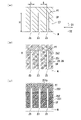
- FIG. 3A is a side view showing a state in which the liquid film 26 of the suspension 25 covers the upper surface of the substrate W.
- FIG. 3(b) is a side view showing an enlarged part of the liquid film 26 of the suspension 25 and part of the substrate W shown in FIG. 3(a).
- the insulating layer is, for example, a silicon oxide film or a silicon nitride film.
- the semiconductor layer is, for example, a polysilicon film or an amorphous silicon film.
- the conductor layer is, for example, a metal film.
- the metal film is, for example, a film containing at least one of titanium, tungsten, copper, and aluminum.
- the density of the particles 252 in the suspension 25 is, for example, a volume fraction of 0.1 or more and 0.9 or less.
- the density of the particles 252 in the suspension 25 is such that, for example, the particles 252 are in the space SP is a value that can occupy more than "M/10" of .
- M is a real number.
- M is, for example, "1", preferably "2", more preferably "3", more preferably "4", more preferably "5", more preferably "6", more preferably "7”
- Preferred is "8", more preferred is "9", and most preferred is "10".
- the more particles 252 occupying the space SP between the structures 23 at the completion of the treatment liquid removal step (FIGS. 4(c) and 5(a)), the more effectively the structure 23 collapses. can be suppressed. Details of this point will be described later.
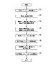
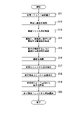
- the process liquid 251 is poured from the upper surface of the substrate W so that the particles 252 remain between the structures 23 adjacent to each other. Eliminate (remove).
- the processing liquid 251 is removed (removed) from the substrate W by rotating the substrate W while the supply of the suspension 25 is stopped.
- step S6 the center robot CR loads the substrate W into the particle removal unit 5.
- the ozone gas supply unit 6B includes an ozone gas supply source 61B, a gas supply pipe 62B, a gas supply valve 63B, and a gas nozzle 64B.
- the gas nozzle 64B has a gas supply port 641B.
- the gas nozzle 64B is connected to the ozone gas supply source 61B via the gas supply pipe 62B. By opening the gas supply valve 63B, ozone (O 3 ) gas is supplied to the processing space 20B from the gas supply port 641B of the gas nozzle 64B.
- a discharge gas exists in the space between the electrodes 33C and 35C.
- a high voltage with a high frequency is applied between the electrodes 33C and 35C.
- the discharge gas is excited into an excimer state.
- the discharge gas generates ultraviolet rays when returning from the excimer state to the ground state.
- the ultraviolet rays pass through the openings 351C of the electrodes 35C, pass through the quartz glass plate 31C, and irradiate the substrate W with the ultraviolet rays.
Landscapes
- Cleaning Or Drying Semiconductors (AREA)
- Physics & Mathematics (AREA)
- High Energy & Nuclear Physics (AREA)
Abstract
Description
図1~図8を参照して、本発明の実施形態1に係る基板処理装置100を説明する。まず、図1を参照して、基板処理装置100を説明する。図1は、基板処理装置100の内部を示す平面図である。図1に示す基板処理装置100は、複数の構造物を含むパターンを有する基板Wを処理する。
図9及び図10を参照して、本発明の実施形態2に係る基板処理装置100を説明する。実施形態2に係る基板処理装置100が懸濁液供給工程の前にリンス液供給工程を実行する点で、実施形態2は実施形態1と主に異なる。その他、実施形態2に係る基板処理装置100の全体構成は、図1を参照して説明した実施形態1に係る基板処理装置100の全体構成と同様である。以下、実施形態2が実施形態1と異なる点を主に説明する。
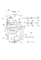
図11は、本発明の一実施形態に係る粒子除去ユニット5を示す模式的断面図である。図11に示す粒子除去ユニット5は、懸濁液25を構成する処理液251がリンス液で、懸濁液25を構成する粒子252がシリカである場合に、処理液251が排除された基板Wの上面にフッ酸の蒸気を供給することで、基板Wの構造物23と構造物23との間から粒子252を除去する。なお、図8の工程S6又は図10の工程S18において、基板Wが粒子除去ユニット5に搬入される。従って、粒子除去ユニット5によって処理される基板Wは、懸濁液25のうちの処理液251(リンス液)が排除されて粒子252(シリカ)が堆積した状態の基板W(図5(a)又は図7(a))である。
図12は、本発明の他の実施形態に係る粒子除去ユニット5を示す模式的断面図である。図12に示す粒子除去ユニット5は、懸濁液25がポリスチレンラテックスである場合に、懸濁液25のうちの処理液251が排除された基板Wの上面にオゾンを供給することで、基板Wの構造物23と構造物23との間から粒子252(ポリスチレン)を除去する。なお、図8の工程S6又は図10の工程S18において、基板Wが粒子除去ユニット5に搬入される。従って、粒子除去ユニット5によって処理される基板Wは、懸濁液25のうちの処理液251(リンス液)が排除されて粒子252(ポリスチレン)が堆積した状態の基板W(図5(a)又は図7(a))である。
図13は、本発明の更に他の実施形態に係る粒子除去ユニット5を示す模式的断面図である。図13に示す粒子除去ユニット5は、懸濁液25がポリスチレンラテックスである場合に、懸濁液25のうちの処理液251が排除された基板Wの上面に紫外線を照射することで、基板Wの構造物23と構造物23との間から粒子252(ポリスチレン)を除去する。なお、図8の工程S6又は図10の工程S18において、基板Wが粒子除去ユニット5に搬入される。従って、粒子除去ユニット5によって処理される基板Wは、懸濁液25のうちの処理液251(リンス液)が排除されて粒子252(ポリスチレン)が堆積した状態の基板W(図5(a)又は図7(a))である。
12 スピンチャック(基板保持部)
13 スピンモーター(基板回転部)
14 薬液ノズル(薬液供給部)
17 懸濁液ノズル(懸濁液供給部)
21 制御部
31 リンス液ノズル(リンス液供給部)
34 基板加熱部
100 基板処理装置
W 基板
Claims (24)
- 複数の構造物を含むパターンを有する基板を処理する基板処理方法であって、
処理液と、前記処理液に溶解しない複数の粒子とが混在した懸濁液を、前記基板の上面に供給することで、前記懸濁液の液膜を前記基板の上面に形成する懸濁液供給工程と、
互いに隣り合う前記構造物と前記構造物との間に前記粒子が残留するように、前記基板の上面から前記処理液を排除する処理液排除工程と
を含む、基板処理方法。 - 非液体によって、前記構造物と前記構造物との間に残留した前記粒子を除去する粒子除去工程を更に含む、請求項1に記載の基板処理方法。
- 前記粒子は、無機物であり、
前記非液体は、薬液の蒸気であり、
前記粒子除去工程では、前記基板の上面に前記薬液の蒸気を供給することで、前記構造物と前記構造物との間から前記粒子を除去する、請求項2に記載の基板処理方法。 - 前記粒子は、シリカである、請求項1から請求項3のいずれか1項に記載の基板処理方法。
- 前記粒子は、有機物であり、
前記非液体は、紫外線又はオゾンであり、
前記粒子除去工程では、前記基板の上面に前記オゾンを供給することで、又は、前記基板の上面に前記紫外線を照射することで、前記構造物と前記構造物との間から前記粒子を除去する、請求項2に記載の基板処理方法。 - 前記粒子は、ポリスチレンである、請求項1から請求項3のいずれか1項に記載の基板処理方法。
- 前記処理液は、リンス液である、請求項1から請求項6のいずれか1項に記載の基板処理方法。
- 前記粒子のサイズは、互いに隣り合う前記構造物と前記構造物との間隔よりも小さい、請求項1から請求項7のいずれか1項に記載の基板処理方法。
- 前記処理液排除工程では、前記基板を回転させることで、前記基板から前記処理液を排除する、請求項1から請求項8のいずれか1項に記載の基板処理方法。
- 前記処理液排除工程の実行時間は、所定工程の実行時間よりも長く、
前記所定工程は、前記処理液と同じ処理液であって、前記粒子の混在しない処理液を、回転によって基板から振り切る工程を示す、請求項9に記載の基板処理方法。 - 前記処理液排除工程よりも後であって、前記粒子除去工程よりも前において、前記基板を加熱する基板加熱工程を更に含む、請求項2に記載の基板処理方法。
- 前記懸濁液供給工程よりも前において、薬液を前記基板の上面に供給する薬液供給工程と、
前記薬液供給工程の次に、リンス液を前記基板の上面に供給することで、前記薬液を洗い流すリンス液供給工程と
を更に含み、
前記懸濁液供給工程は、前記リンス液供給工程の次に実行される、請求項1から請求項11のいずれか1項に記載の基板処理方法。 - 複数の構造物を含むパターンを有する基板を処理する基板処理装置であって、
処理液と、前記処理液に溶解しない複数の粒子とが混在した懸濁液を、前記基板の上面に供給することで、前記懸濁液の液膜を前記基板の上面に形成する懸濁液供給部と、
処理液排除制御を実行する制御部と
を更に備え、
前記処理液排除制御は、互いに隣り合う前記構造物と前記構造物との間に前記粒子を残留させつつ、前記基板の上面から前記処理液を排除する制御を示す、基板処理装置。 - 非液体によって、前記構造物と前記構造物との間に残留した前記粒子を除去する粒子除去ユニットを更に備える、請求項13に記載の基板処理装置。
- 前記粒子は、無機物であり、
前記非液体は、薬液の蒸気であり、
前記粒子除去ユニットは、前記基板の上面に前記薬液の蒸気を供給することで、前記構造物と前記構造物との間から前記粒子を除去する、請求項14に記載の基板処理装置。 - 前記粒子は、シリカである、請求項13から請求項15のいずれか1項に記載の基板処理装置。
- 前記粒子は、有機物であり、
前記非液体は、紫外線又はオゾンであり、
前記粒子除去ユニットは、前記基板の上面に前記オゾンを供給することで、又は、前記基板の上面に前記紫外線を照射することで、前記構造物と前記構造物との間から前記粒子を除去する、請求項14に記載の基板処理装置。 - 前記粒子は、ポリスチレンである、請求項13から請求項15のいずれか1項に記載の基板処理装置。
- 前記処理液は、リンス液である、請求項13から請求項18のいずれか1項に記載の基板処理装置。
- 前記粒子のサイズは、互いに隣り合う前記構造物と前記構造物との間隔よりも小さい、請求項13から請求項19のいずれか1項に記載の基板処理装置。
- 前記基板を保持する基板保持部と、
前記基板保持部を回転させることで、前記基板を回転させる基板回転部と
を更に備え、
前記処理液排除制御は、前記基板回転部によって前記基板を回転させる制御を示す、請求項13から請求項20のいずれか1項に記載の基板処理装置。 - 前記処理液排除制御の実行時間は、所定工程の実行時間よりも長く、
前記所定工程は、前記処理液と同じ処理液であって、前記粒子の混在しない処理液を、回転によって基板から振り切る工程を示す、請求項21に記載の基板処理装置。 - 前記処理液排除制御の実行時よりも後であって、前記粒子除去ユニットによる前記粒子の除去処理よりも前において、前記基板を加熱する基板加熱部を更に備える、請求項14に記載の基板処理装置。
- 前記懸濁液供給部による前記懸濁液の供給処理よりも前において、薬液を前記基板の上面に供給する薬液供給部と、
前記薬液供給部による前記薬液の供給処理の次に、リンス液を前記基板の上面に供給することで、前記薬液を洗い流すリンス液供給部と
を更に備え、
前記懸濁液供給部は、前記リンス液供給部による前記リンス液の供給処理の次に、前記基板の上面に前記懸濁液を供給する、請求項13から請求項23のいずれか1項に記載の基板処理装置。
Priority Applications (1)
| Application Number | Priority Date | Filing Date | Title |
|---|---|---|---|
| KR1020237029143A KR102839844B1 (ko) | 2021-03-25 | 2022-01-25 | 기판 처리 방법 및 기판 처리 장치 |
Applications Claiming Priority (2)
| Application Number | Priority Date | Filing Date | Title |
|---|---|---|---|
| JP2021051569A JP7633058B2 (ja) | 2021-03-25 | 2021-03-25 | 基板処理方法及び基板処理装置 |
| JP2021-051569 | 2021-03-25 |
Publications (1)
| Publication Number | Publication Date |
|---|---|
| WO2022201830A1 true WO2022201830A1 (ja) | 2022-09-29 |
Family
ID=83395333
Family Applications (1)
| Application Number | Title | Priority Date | Filing Date |
|---|---|---|---|
| PCT/JP2022/002647 Ceased WO2022201830A1 (ja) | 2021-03-25 | 2022-01-25 | 基板処理方法及び基板処理装置 |
Country Status (4)
| Country | Link |
|---|---|
| JP (1) | JP7633058B2 (ja) |
| KR (1) | KR102839844B1 (ja) |
| TW (1) | TWI831129B (ja) |
| WO (1) | WO2022201830A1 (ja) |
Citations (3)
| Publication number | Priority date | Publication date | Assignee | Title |
|---|---|---|---|---|
| JPH10275788A (ja) * | 1997-03-31 | 1998-10-13 | Sumitomo Chem Co Ltd | 半導体装置の製造方法及び半導体装置の製造装置 |
| JP2010518230A (ja) * | 2007-02-08 | 2010-05-27 | フォンタナ・テクノロジー | パーティクル除去方法及び組成物 |
| JP2018157107A (ja) * | 2017-03-17 | 2018-10-04 | 東芝メモリ株式会社 | テンプレート洗浄方法、テンプレート洗浄装置、及び洗浄液 |
Family Cites Families (3)
| Publication number | Priority date | Publication date | Assignee | Title |
|---|---|---|---|---|
| CN103430102B (zh) * | 2011-03-18 | 2017-02-08 | 巴斯夫欧洲公司 | 制造具有带50nm及更小行间距尺寸的图案化材料层的集成电路装置、光学装置、微型电机和机械精密装置的方法 |
| TW201712752A (zh) * | 2015-06-04 | 2017-04-01 | 蘭姆研究公司 | 高深寬比結構之不造成坍陷的乾燥方法 |
| JP6703858B2 (ja) | 2016-02-26 | 2020-06-03 | 株式会社Screenホールディングス | 基板処理装置および基板処理方法 |
-
2021
- 2021-03-25 JP JP2021051569A patent/JP7633058B2/ja active Active
-
2022
- 2022-01-25 KR KR1020237029143A patent/KR102839844B1/ko active Active
- 2022-01-25 WO PCT/JP2022/002647 patent/WO2022201830A1/ja not_active Ceased
- 2022-02-14 TW TW111105187A patent/TWI831129B/zh active
Patent Citations (3)
| Publication number | Priority date | Publication date | Assignee | Title |
|---|---|---|---|---|
| JPH10275788A (ja) * | 1997-03-31 | 1998-10-13 | Sumitomo Chem Co Ltd | 半導体装置の製造方法及び半導体装置の製造装置 |
| JP2010518230A (ja) * | 2007-02-08 | 2010-05-27 | フォンタナ・テクノロジー | パーティクル除去方法及び組成物 |
| JP2018157107A (ja) * | 2017-03-17 | 2018-10-04 | 東芝メモリ株式会社 | テンプレート洗浄方法、テンプレート洗浄装置、及び洗浄液 |
Also Published As
| Publication number | Publication date |
|---|---|
| JP2022149423A (ja) | 2022-10-06 |
| KR102839844B1 (ko) | 2025-07-29 |
| JP7633058B2 (ja) | 2025-02-19 |
| TWI831129B (zh) | 2024-02-01 |
| TW202242981A (zh) | 2022-11-01 |
| KR20230135658A (ko) | 2023-09-25 |
Similar Documents
| Publication | Publication Date | Title |
|---|---|---|
| JP6728009B2 (ja) | 基板処理方法および基板処理装置 | |
| JP6881922B2 (ja) | 基板処理方法および基板処理装置 | |
| JP6875811B2 (ja) | パターン倒壊回復方法、基板処理方法および基板処理装置 | |
| JP6672023B2 (ja) | 基板処理方法および基板処理装置 | |
| KR102518117B1 (ko) | 기판 처리 방법 및 기판 처리 장치 | |
| WO2017029862A1 (ja) | 基板処理方法および基板処理装置 | |
| JP2020004908A (ja) | 基板処理方法および基板処理装置 | |
| JP2022090061A (ja) | 基板処理方法および基板処理装置 | |
| JP2017041512A (ja) | 基板処理方法および基板処理装置 | |
| WO2020021903A1 (ja) | 基板処理方法および基板処理装置 | |
| JP7311988B2 (ja) | 基板処理方法、半導体製造方法、および、基板処理装置 | |
| WO2023090171A1 (ja) | 基板処理方法 | |
| WO2020105376A1 (ja) | 基板処理方法および基板処理装置 | |
| JP7633058B2 (ja) | 基板処理方法及び基板処理装置 | |
| WO2020195695A1 (ja) | 基板処理装置、基板処理方法および半導体製造方法 | |
| WO2024210065A1 (ja) | 基板処理方法 | |
| WO2023008529A1 (ja) | 基板処理方法及び基板処理装置 | |
| JP7603517B2 (ja) | 基板処理方法、および、基板処理装置 | |
| TW202301424A (zh) | 基板處理方法及基板處理裝置 | |
| JP2021073736A (ja) | 基板処理方法および基板処理装置 |
Legal Events
| Date | Code | Title | Description |
|---|---|---|---|
| 121 | Ep: the epo has been informed by wipo that ep was designated in this application |
Ref document number: 22774632 Country of ref document: EP Kind code of ref document: A1 |
|
| ENP | Entry into the national phase |
Ref document number: 20237029143 Country of ref document: KR Kind code of ref document: A |
|
| WWE | Wipo information: entry into national phase |
Ref document number: 1020237029143 Country of ref document: KR |
|
| NENP | Non-entry into the national phase |
Ref country code: DE |
|
| 122 | Ep: pct application non-entry in european phase |
Ref document number: 22774632 Country of ref document: EP Kind code of ref document: A1 |