WO2022201635A1 - Iii族元素窒化物半導体基板 - Google Patents
Iii族元素窒化物半導体基板 Download PDFInfo
- Publication number
- WO2022201635A1 WO2022201635A1 PCT/JP2021/042574 JP2021042574W WO2022201635A1 WO 2022201635 A1 WO2022201635 A1 WO 2022201635A1 JP 2021042574 W JP2021042574 W JP 2021042574W WO 2022201635 A1 WO2022201635 A1 WO 2022201635A1
- Authority
- WO
- WIPO (PCT)
- Prior art keywords
- group iii
- iii element
- nitride semiconductor
- substrate
- semiconductor substrate
- Prior art date
- Legal status (The legal status is an assumption and is not a legal conclusion. Google has not performed a legal analysis and makes no representation as to the accuracy of the status listed.)
- Ceased
Links
Images

Classifications
-
- C—CHEMISTRY; METALLURGY
- C30—CRYSTAL GROWTH
- C30B—SINGLE-CRYSTAL GROWTH; UNIDIRECTIONAL SOLIDIFICATION OF EUTECTIC MATERIAL OR UNIDIRECTIONAL DEMIXING OF EUTECTOID MATERIAL; REFINING BY ZONE-MELTING OF MATERIAL; PRODUCTION OF A HOMOGENEOUS POLYCRYSTALLINE MATERIAL WITH DEFINED STRUCTURE; SINGLE CRYSTALS OR HOMOGENEOUS POLYCRYSTALLINE MATERIAL WITH DEFINED STRUCTURE; AFTER-TREATMENT OF SINGLE CRYSTALS OR A HOMOGENEOUS POLYCRYSTALLINE MATERIAL WITH DEFINED STRUCTURE; APPARATUS THEREFOR
- C30B29/00—Single crystals or homogeneous polycrystalline material with defined structure characterised by the material or by their shape
- C30B29/10—Inorganic compounds or compositions
- C30B29/40—AIIIBV compounds wherein A is B, Al, Ga, In or Tl and B is N, P, As, Sb or Bi
- C30B29/403—AIII-nitrides
- C30B29/406—Gallium nitride
-
- H—ELECTRICITY
- H10—SEMICONDUCTOR DEVICES; ELECTRIC SOLID-STATE DEVICES NOT OTHERWISE PROVIDED FOR
- H10P—GENERIC PROCESSES OR APPARATUS FOR THE MANUFACTURE OR TREATMENT OF DEVICES COVERED BY CLASS H10
- H10P14/00—Formation of materials, e.g. in the shape of layers or pillars
- H10P14/20—Formation of materials, e.g. in the shape of layers or pillars of semiconductor materials
- H10P14/29—Formation of materials, e.g. in the shape of layers or pillars of semiconductor materials characterised by the substrates
- H10P14/2901—Materials
- H10P14/2907—Materials being Group IIIA-VA materials
- H10P14/2908—Nitrides
-
- C—CHEMISTRY; METALLURGY
- C30—CRYSTAL GROWTH
- C30B—SINGLE-CRYSTAL GROWTH; UNIDIRECTIONAL SOLIDIFICATION OF EUTECTIC MATERIAL OR UNIDIRECTIONAL DEMIXING OF EUTECTOID MATERIAL; REFINING BY ZONE-MELTING OF MATERIAL; PRODUCTION OF A HOMOGENEOUS POLYCRYSTALLINE MATERIAL WITH DEFINED STRUCTURE; SINGLE CRYSTALS OR HOMOGENEOUS POLYCRYSTALLINE MATERIAL WITH DEFINED STRUCTURE; AFTER-TREATMENT OF SINGLE CRYSTALS OR A HOMOGENEOUS POLYCRYSTALLINE MATERIAL WITH DEFINED STRUCTURE; APPARATUS THEREFOR
- C30B9/00—Single-crystal growth from melt solutions using molten solvents
- C30B9/04—Single-crystal growth from melt solutions using molten solvents by cooling of the solution
- C30B9/08—Single-crystal growth from melt solutions using molten solvents by cooling of the solution using other solvents
- C30B9/10—Metal solvents
-
- H—ELECTRICITY
- H10—SEMICONDUCTOR DEVICES; ELECTRIC SOLID-STATE DEVICES NOT OTHERWISE PROVIDED FOR
- H10D—INORGANIC ELECTRIC SEMICONDUCTOR DEVICES
- H10D62/00—Semiconductor bodies, or regions thereof, of devices having potential barriers
- H10D62/40—Crystalline structures
- H10D62/405—Orientations of crystalline planes
-
- H—ELECTRICITY
- H10—SEMICONDUCTOR DEVICES; ELECTRIC SOLID-STATE DEVICES NOT OTHERWISE PROVIDED FOR
- H10D—INORGANIC ELECTRIC SEMICONDUCTOR DEVICES
- H10D62/00—Semiconductor bodies, or regions thereof, of devices having potential barriers
- H10D62/80—Semiconductor bodies, or regions thereof, of devices having potential barriers characterised by the materials
- H10D62/85—Semiconductor bodies, or regions thereof, of devices having potential barriers characterised by the materials being Group III-V materials, e.g. GaAs
- H10D62/8503—Nitride Group III-V materials, e.g. AlN or GaN
-
- H—ELECTRICITY
- H10—SEMICONDUCTOR DEVICES; ELECTRIC SOLID-STATE DEVICES NOT OTHERWISE PROVIDED FOR
- H10H—INORGANIC LIGHT-EMITTING SEMICONDUCTOR DEVICES HAVING POTENTIAL BARRIERS
- H10H20/00—Individual inorganic light-emitting semiconductor devices having potential barriers, e.g. light-emitting diodes [LED]
- H10H20/01—Manufacture or treatment
- H10H20/011—Manufacture or treatment of bodies, e.g. forming semiconductor layers
- H10H20/013—Manufacture or treatment of bodies, e.g. forming semiconductor layers having light-emitting regions comprising only Group III-V materials
- H10H20/0137—Manufacture or treatment of bodies, e.g. forming semiconductor layers having light-emitting regions comprising only Group III-V materials the light-emitting regions comprising nitride materials
-
- H—ELECTRICITY
- H10—SEMICONDUCTOR DEVICES; ELECTRIC SOLID-STATE DEVICES NOT OTHERWISE PROVIDED FOR
- H10H—INORGANIC LIGHT-EMITTING SEMICONDUCTOR DEVICES HAVING POTENTIAL BARRIERS
- H10H20/00—Individual inorganic light-emitting semiconductor devices having potential barriers, e.g. light-emitting diodes [LED]
- H10H20/80—Constructional details
- H10H20/81—Bodies
- H10H20/817—Bodies characterised by the crystal structures or orientations, e.g. polycrystalline, amorphous or porous
- H10H20/818—Bodies characterised by the crystal structures or orientations, e.g. polycrystalline, amorphous or porous within the light-emitting regions
-
- H—ELECTRICITY
- H10—SEMICONDUCTOR DEVICES; ELECTRIC SOLID-STATE DEVICES NOT OTHERWISE PROVIDED FOR
- H10H—INORGANIC LIGHT-EMITTING SEMICONDUCTOR DEVICES HAVING POTENTIAL BARRIERS
- H10H20/00—Individual inorganic light-emitting semiconductor devices having potential barriers, e.g. light-emitting diodes [LED]
- H10H20/80—Constructional details
- H10H20/81—Bodies
- H10H20/822—Materials of the light-emitting regions
- H10H20/824—Materials of the light-emitting regions comprising only Group III-V materials, e.g. GaP
- H10H20/825—Materials of the light-emitting regions comprising only Group III-V materials, e.g. GaP containing nitrogen, e.g. GaN
-
- H—ELECTRICITY
- H10—SEMICONDUCTOR DEVICES; ELECTRIC SOLID-STATE DEVICES NOT OTHERWISE PROVIDED FOR
- H10P—GENERIC PROCESSES OR APPARATUS FOR THE MANUFACTURE OR TREATMENT OF DEVICES COVERED BY CLASS H10
- H10P14/00—Formation of materials, e.g. in the shape of layers or pillars
- H10P14/20—Formation of materials, e.g. in the shape of layers or pillars of semiconductor materials
- H10P14/29—Formation of materials, e.g. in the shape of layers or pillars of semiconductor materials characterised by the substrates
- H10P14/2926—Crystal orientations
Definitions
- the present invention relates to a Group III element nitride semiconductor substrate.
- Group III element nitride semiconductor substrates such as gallium nitride (GaN) wafers, aluminum nitride (AlN) wafers, and indium nitride (InN) wafers are used as substrates for various semiconductor devices.
- GaN gallium nitride
- AlN aluminum nitride
- InN indium nitride
- the semiconductor substrate has a first surface and a second surface.
- the main surface is typically the Group III element polar surface
- the back surface is typically the nitrogen polar surface.
- Epitaxial crystals can be grown on the main surface, and various devices can be manufactured.
- a group III element nitride layer is grown on a base substrate such as a sapphire substrate to form a layer, the base substrate is separated by LLO (laser lift-off) technology or the like, and a self-supporting layer made of the group III element nitride is formed. It is known to obtain substrates. Light-emitting elements such as LEDs and LDs and power devices are manufactured by forming functional layers such as GaN, AlGaN, and InGaN on such self-supporting substrates. Recently, there has been a demand for large-diameter base substrates of 4 inches and 6 inches for ultra-high brightness LEDs and power devices.
- the off-angle distribution in the group III element nitride semiconductor substrate is large, the surface morphology of the functional layer formed on the group III element nitride semiconductor substrate becomes rough, and the function varies depending on the location. For example, in the case of a light-emitting device, there arises a problem that the wavelength variation within the substrate becomes large.
- An object of the present invention is to provide a Group III element nitride semiconductor substrate with a small off-angle distribution.
- a Group III element nitride semiconductor substrate comprises A Group III element nitride semiconductor substrate comprising a first surface and a second surface, The curvature of the crystal plane of the first plane has a plurality of poles.
- the warpage of the crystal plane in the ⁇ 11-20> direction passing through the center of the substrate of the crystal plane of the first plane and the ⁇ 1- Any warp of the crystal plane in the 100> direction has a plurality of poles.
- the number of poles is 3 or more.
- the distance between adjacent poles is 3 mm or more.
- the off-angle distribution of the entire Group III element nitride semiconductor substrate is 0.40° or less.
- the diameter of the Group III element nitride semiconductor substrate is 75 mm or more.
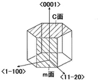
- FIG. 1 is a representative schematic perspective view of a III-nitride semiconductor substrate according to embodiments of the present invention
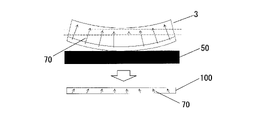
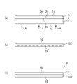
- FIG. FIG. 2 is a schematic cross-sectional view representative of the process of flattening a group III element nitride layer to form a flat group III element nitride semiconductor substrate.
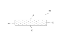
- 1 is a representative schematic cross-sectional view of a III-nitride semiconductor substrate according to an embodiment of the invention
- FIG. 1 is a representative schematic cross-sectional view of a III-nitride semiconductor substrate according to an embodiment of the invention
- FIG. It is a schematic explanatory drawing which shows the manufacturing method of the group III element nitride semiconductor substrate by embodiment of this invention.
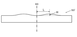
- FIG. 11 is a schematic cross-sectional view through the center of a ceramic processing platen used in Example 6;
- weight When the term “weight” is used in this specification, it may be read as “mass”, which is commonly used as an SI unit indicating weight.
- a group III element nitride semiconductor substrate according to an embodiment of the present invention is typically a self-supporting substrate made of a group III element nitride crystal.
- the term "self-supporting substrate” means a substrate that does not deform or break under its own weight during handling and can be handled as a solid object.
- the self-supporting substrate can be used as a substrate for various semiconductor devices such as light emitting elements and power control elements.
- the Group III element nitride semiconductor substrate according to the embodiment of the present invention is typically wafer-shaped (substantially circular). However, if necessary, it may be processed into other shapes such as a rectangular shape.
- any appropriate diameter can be adopted as the diameter of the group III element nitride semiconductor substrate according to the embodiment of the present invention, as long as the effects of the present invention are not impaired.
- a diameter is, for example, 50 mm or more.
- the diameter of the Group III element nitride semiconductor substrate according to the embodiment of the present invention is preferably 75 mm or more, and more preferably 100 mm or more, in order to make the effects of the present invention more manifest.
- the group III element nitride semiconductor substrate according to the embodiment of the present invention is a so-called large-diameter group III element nitride semiconductor substrate having a diameter of 75 mm or more
- the group III element nitride semiconductor according to the embodiment of the present invention can be easily applied to high-frequency/high-power electronic devices, and in particular, to devices that handle large power such that the device size is large.
- Group III element nitride semiconductor substrates include 4-inch wafers, 6-inch wafers, 8-inch wafers, and 12-inch wafers.
- the thickness of the group III element nitride semiconductor substrate according to the embodiment of the present invention is preferably 300 ⁇ m to 1000 ⁇ m.
- Group III element nitrides typically include gallium nitride (GaN), aluminum nitride (AlN), indium nitride (InN), or mixed crystals thereof. These may be of only one type, or may be of two or more types.
- P-type dopants typically include beryllium (Be), magnesium (Mg), strontium (Sr), and cadmium (Cd). These may be of only one type, or may be of two or more types.
- Typical n-type dopants include silicon (Si), germanium (Ge), tin (Sn), and oxygen (O). These may be of only one type, or may be of two or more types.
- a group III element nitride semiconductor substrate is a group III element nitride semiconductor substrate having a first surface and a second surface.
- the main surface is typically the group III element polar plane.
- the back surface is typically a nitrogen polar surface.
- the main surface may be a nitrogen polar surface
- the rear surface may be a Group III element polar surface.
- Epitaxial crystals can be grown on the main surface, and various devices can be fabricated.
- the back surface can be held by a susceptor or the like to transfer the III-nitride semiconductor substrate according to embodiments of the invention.
- the first surface is the main surface and the second surface is the back surface. Therefore, in this specification, “main surface” may be read as “first surface”, “first surface” may be read as “main surface”, and “back surface” may be read. A thing may be read as a “second side”, and a thing with a “second side” may be read as a "back side”.
- FIG. 1 is a schematic explanatory diagram illustrating the plane orientation and crystal plane in the crystal structure of the group III element nitride semiconductor substrate according to the embodiment of the present invention.
- the ⁇ 0001> direction is the c-axis direction
- the ⁇ 1-100> direction is the m-axis direction
- the ⁇ 11-20> direction is the a-axis direction.
- the upper surface of the hexagonal crystal that can be regarded as a regular hexagonal prism is the c-plane
- the sidewall surface of the regular hexagonal prism is the m-plane.
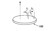
- FIG. 2 is a representative schematic perspective view of a III-nitride semiconductor substrate 100 according to an embodiment of the invention.
- the c-axis ( ⁇ 0001> direction) is inclined with respect to the normal vector A of the first surface. That is, the group III element nitride semiconductor substrate 100 according to the embodiment of the present invention has an off angle ⁇ which is the tilt angle of the c-axis ( ⁇ 0001> direction) with respect to the normal vector A of the first surface.
- This off-angle ⁇ can vary depending on the crystal state of the c-axis location in the first plane.
- a conventional Group III element nitride semiconductor substrate generally, as shown in FIG. angle ⁇ 2 ), resulting in an off-angle distribution when viewing the entire first surface.
- a group III element nitride semiconductor substrate is formed by growing a group III element nitride layer on an underlying substrate such as a sapphire substrate, and then growing the group III element nitride layer from the underlying substrate by LLO (laser lift-off) technology or the like. to obtain a Group III element nitride semiconductor substrate therefrom.
- LLO laser lift-off
- the group III element nitride layer separated from the underlying substrate warps concavely due to the stress distribution inside the group III element nitride crystal, the dislocation density difference between the front and back sides of the group III element nitride layer, and the like.
- the off-angle of the underlying substrate is approximately the same value at any location on the substrate, and the off-angle distribution is approximately uniform, even in the group III element nitride layer grown and formed thereon, the In this state, the off-angle is close to the off-angle of the base substrate at any point on the layer surface, and the off-angle distribution is almost uniform. Then, even if the group III element nitride layer is warped concavely by separating the group III element nitride layer from the underlying substrate, the normal vector of the tangential plane at that position is warped at any position on the layer surface.
- the off-angle which is the inclination angle of the c-axis ( ⁇ 0001> direction) with respect to the normal vector, does not substantially change from before the warp, and the off-angle distribution is substantially uniform.
- a flat group III element nitride semiconductor substrate 100 is formed by planarization.
- the warped group III element nitride layer 3 is flattened to form a flat group III element nitride semiconductor substrate 100, this flattening process eliminates the warpage of the outer shape of the substrate itself.
- the Group III element nitride layer which has a substantially uniform off-angle distribution in the warped state, is planarized, a region is formed in which the off-angle deviates from the originally intended crystal orientation, as shown in FIG. As the position approaches the outer periphery of the substrate, the deviation width increases, and an off-angle distribution occurs when the entire first surface is viewed.
- the warped group III element nitride layer is attached to a processing surface plate in a flattened state, followed by flattening processing. , the amount of deformation of the obtained group III element nitride semiconductor substrate becomes large, and the group III element nitride semiconductor substrate cracks. Since the size of the outer shape of such a warped group III element nitride layer increases in proportion to the square of the diameter, it becomes a significant problem especially in large-diameter substrates of 4 inches or more.
- the surface morphology of the functional layer formed on the group III element nitride semiconductor substrate may be roughened, and the function may vary depending on the location. For example, in the case of a light-emitting device, there arises a problem that the wavelength variation within the substrate increases.
- the group III element nitride semiconductor substrate according to the embodiment of the present invention is a group III element nitride semiconductor substrate having a small off-angle distribution, and the off-angle distribution of the entire group III element nitride semiconductor substrate is preferably 0.40. ° or less, more preferably 0.30° or less, still more preferably 0.20° or less, particularly preferably 0.10° or less, and most preferably 0.06° or less. If the off-angle distribution of the group III element nitride semiconductor substrate according to the embodiment of the present invention is within the above range, the surface morphology of the functional layer formed on the group III element nitride semiconductor substrate is less likely to be roughened. This reduces the possibility that the function will vary depending on the location.
- the warp of the crystal plane of the first plane has a plurality of poles. Since the warp of the crystal plane of the first plane has a plurality of poles in this way, the deviation width of the off-angle from the originally intended crystal orientation within the entire first plane is reduced, and the off-angle distribution is reduced. can be.
- FIG. 4 is a representative schematic cross-sectional view of a III-nitride semiconductor substrate according to an embodiment of the invention.
- An arrow 80 indicates the component ⁇ a in the ⁇ 11-20> direction (a-axis direction) of the off angle ⁇ measured on the surface of the group III element nitride semiconductor substrate 100 according to the embodiment of the present invention. It indicates any component ⁇ m in the ⁇ 1-100> direction ( m -axis direction) perpendicular to the direction.
- An arrow 85 is a normal line on the substrate surface
- a curve 90 is a schematic of an off-angle approximation curve in the ⁇ 11-20> or ⁇ 1-100> direction
- + and - are the signs of the differential coefficient at each off-angle measurement point. .
- the "pole" of the warpage of the first crystal plane is defined as follows. First, let the tilt angle of the c-axis ( ⁇ 0001> direction) with respect to the normal vector A of the first surface be an off angle ⁇ . Let ⁇ a be the component of the off angle ⁇ in the ⁇ 11-20> direction (a-axis direction), and let ⁇ m be the component in the ⁇ 1-100> direction (m-axis direction) perpendicular to the ⁇ 11-20> direction. .
- the off angle can be measured by an X-ray diffraction method.
- the measurement coordinates are in a direction parallel to the ⁇ 11-20> direction (a-axis direction) passing through the center of the substrate and in a ⁇ 1-100> direction (m-axis direction) orthogonal to that direction and passing through the center of the substrate. , from the edge of the substrate to the edge of the opposite substrate at intervals of 2 mm. However, the area within 3 mm from the edge of the substrate is excluded.
- ⁇ a at the measurement coordinates and ⁇ m at the measurement coordinates approximate curves are drawn using spline curves. Then, the differential coefficient at each measurement point is obtained, and one pole is defined when the plus/minus sign of the differential coefficient changes from plus to minus or from minus to plus between adjacent coordinates.
- the center of the substrate refers to the center of the maximum possible length on the substrate.
- the group III element nitride semiconductor substrate according to the embodiment of the present invention preferably has a crystal plane warp in the ⁇ 11-20> direction passing through the center of the substrate of the crystal plane of the first plane and the ⁇ 11-20> direction
- Each of the crystal plane warpages in the ⁇ 1-100> direction passing through the center of the orthogonal substrate has a plurality of poles.
- the number of "poles" of the warp of the crystal plane of the first plane is preferably 3 or more, more preferably 3 to 100, still more preferably 3 to 50, still more preferably 3 to 30. , particularly preferably 3-20, most preferably 3-18.
- the distance between adjacent poles is preferably 3 mm or more, more preferably 5 mm, in the "poles" of the warpage of the crystal plane of the first surface. more preferably 8 mm or more, and particularly preferably 12 mm to (R/4) mm, where R (mm) is the diameter of the substrate.
- R (mm) is the diameter of the substrate.
- FIG. 5 is a representative schematic cross-sectional view of a Group III element nitride semiconductor substrate according to an embodiment of the present invention.
- a group III element nitride semiconductor substrate 100 according to an embodiment of the present invention typically has a main surface (group III element polar surface) 10 and a back surface (nitrogen polar surface) 20 .
- a III-nitride semiconductor substrate 100 according to embodiments of the present invention may have a side surface 30 .
- the end portion of the group III element nitride semiconductor substrate according to the embodiment of the present invention can take any appropriate form within the range that does not impair the effects of the present invention.
- the end portion of the group III element nitride semiconductor substrate according to the embodiment of the present invention has, for example, a chamfered shape such that the chamfered portions on the main surface side and the back surface side are flat surfaces, and the chamfered portions on the main surface side and the back surface side.
- the chamfered portion may be provided over the entire circumference of the outer circumference, or may be part of the outer circumference. may be provided only in
- the Group III element nitride semiconductor substrates according to the embodiments of the present invention can be manufactured by any appropriate method within the range that does not impair the effects of the present invention.
- a preferred method for manufacturing a Group III element nitride semiconductor substrate according to an embodiment of the present invention will be described from the point of view of exhibiting the effects of the present invention.
- a Group III element nitride semiconductor substrate according to an embodiment of the present invention is typically produced by forming a seed crystal film 2 on a main surface 1a of a base substrate 1, as shown in FIG.
- a group III element nitride layer 3 is formed on the group III element polar plane 2 a of 2 .
- the group III element nitride layer (seed crystal film 2 + group III element nitride layer 3) to be a free-standing substrate is separated from the base substrate 1 to obtain a free-standing substrate 100' having a main surface 10' and a rear surface 20'.
- any appropriate material can be used as the material of the base substrate as long as the effects of the present invention are not impaired.
- examples of such materials include sapphire, crystal-oriented alumina, gallium oxide, Al x Ga 1-x N (0 ⁇ x ⁇ 1), GaAs, SiC, silicon, MgO single crystal, ZnO single crystal, spinel ( MgAl 2 O 4 ), LiAlO 2 , LiGaO 2 , LaAlO 3 , LaGaO 3 , NdGaO 3 and other perovskite-type composite oxides.
- any appropriate material can be adopted as the material of the seed crystal film as long as the effects of the present invention are not impaired.
- examples of such materials include Al x Ga 1-x N (0 ⁇ x ⁇ 1) and In x Ga 1-x N (0 ⁇ x ⁇ 1), preferably gallium nitride. More preferably, the material for the seed crystal film is gallium nitride, which has a yellow luminous effect when observed with a fluorescence microscope. Yellow emission is band-to-band exciton transitions (UV) plus peaks appearing in the range 2.2-2.5 eV (yellow emission (YL) or yellow band (YB)).
- UV band-to-band exciton transitions
- YL yellow emission
- YB yellow band
- any appropriate forming method can be adopted as long as the effects of the present invention are not impaired.
- Such formation methods include, for example, a vapor phase epitaxy method, preferably a metal-organic chemical vapor deposition (MOCVD) method, a hydride vapor phase epitaxy (HVPE) method, and a pulse excitation method.
- MOCVD metal-organic chemical vapor deposition
- HVPE hydride vapor phase epitaxy
- PXD deposition
- MBE method MBE method
- sublimation method can be mentioned.
- MOCVD metal-organic chemical vapor deposition
- MOCVD metal-organic chemical vapor deposition
- the seed crystal film is formed by the MOCVD method, for example, after depositing a low-temperature growth buffer layer of 20 nm to 50 nm at 450° C. to 550° C., laminating a film of 2 ⁇ m to 4 ⁇ m in thickness at 1000° C. to 1200° C. It is preferable to carry out by
- any appropriate growth direction can be adopted as the growth direction of the group III element nitride crystal layer within a range that does not impair the effects of the present invention.
- Such growth directions include, for example, the normal direction of the c-plane of the wurtzite structure, the normal directions of each of the a-plane and m-plane, and the normal directions of planes inclined from each of the c-plane, a-plane and m-plane. mentioned.
- any suitable method may be used as long as the method has a crystal orientation that roughly follows the crystal orientation of the seed crystal film, as long as it does not impair the effects of the present invention.
- Such formation methods include, for example, a metal-organic chemical vapor deposition (MOCVD) method, a hydride vapor phase epitaxy (HVPE) method, a pulsed excitation deposition (PXD) method, an MBE method, and a sublimation method.
- MOCVD metal-organic chemical vapor deposition
- HVPE hydride vapor phase epitaxy
- PXD pulsed excitation deposition
- MBE method an MBE method
- sublimation method sublimation method.
- liquid phase growth methods such as Na flux method, ammonothermal method, hydrothermal method and sol-gel method; powder growth methods utilizing solid phase growth of powder; combinations thereof;
- the Na flux method is adopted as the method for forming the group III element nitride crystal layer, the conditions are appropriately adjusted so that the effect of the present invention can be exhibited more according to the manufacturing method described in Japanese Patent No. 5244628. Then, it is preferable to perform the Na flux method.
- any appropriate method can be adopted as the method for separating the group III element nitride crystal layer from the underlying substrate as long as the effects of the present invention are not impaired.
- Examples of such a method include, for example, a method of spontaneously separating the group III element nitride crystal layer from the underlying substrate by using the difference in thermal contraction in the cooling step after growing the group III element nitride crystal layer; A method of separating the nitride crystal layer from the underlying substrate by chemical etching, as shown in FIG. Examples include a method of separating the layer from the base substrate by a laser lift-off method, a method of removing the Group III element nitride crystal layer from the base substrate by grinding, and the like.
- a self-supporting substrate containing the group III element nitride crystal layer may be obtained by slicing the group III element nitride crystal layer using a wire saw or the like.
- the outer periphery of the self-supporting substrate is ground to form a circular shape with a desired diameter.
- any appropriate size can be adopted as the size of the self-supporting substrate as long as the effects of the present invention are not impaired.
- Such sizes include, for example, 20 to 30 mm (about 1 inch), 45 to 55 mm (about 2 inches), 95 to 105 mm (about 4 inches), 145 to 155 mm (about 6 inches), 195 to 205 mm (about 8 inches), 295-305 mm (about 12 inches), and so on.
- the nitrogen-polar surface of the circular self-supporting substrate is attached to the processing surface plate.
- the wax thickness can be changed by adjusting the load applied to the free-standing substrate, a jig can be inserted between the free-standing substrate and the processing surface plate, or the surface can be processed into the desired substrate surface shape.
- a board is used to change the surface topography of the free-standing substrate.
- the off-angle distribution of the group III element polar plane of the free-standing substrate is , preferably 0.40° or less (more preferably 0.30° or less, still more preferably 0.20° or less, particularly preferably 0.10° or less, most preferably 0.06° or less)
- Means are employed for providing a plurality of irregularities on the nitrogen-polar surface of the free-standing substrate.
- Examples of such means include a method of interposing a spacer between the nitrogen polar surface of the self-supporting substrate and the processing surface plate, and a method of making the surface of the processing surface plate facing the nitrogen polar surface of the self-supporting substrate uneven. be done.
- any appropriate spacer can be adopted as the spacer as long as it does not impair the effects of the present invention.
- such spacers include, for example, metal foil (aluminum foil, etc.), paper, medicine packaging paper (parapin), ultrafine wire, resin (silicon sheet, etc.), weak adhesive tape, and the like. is mentioned. Only one type of spacer may be used, or two or more types may be used.
- any suitable shape can be adopted as the shape of the spacer as long as it does not impair the effects of the present invention.
- a shape is preferably a circular ring (donut shape) or a strip shape, and more preferably a circular ring (doughnut shape), in order to make the effects of the present invention more manifest.
- the number of spacers to be used may be one or plural.
- any suitable arrangement position can be adopted as long as the arrangement position does not impair the effects of the present invention. From the point of view that the effects of the present invention can be exhibited more effectively, it is preferable to arrange the spacer so that the center of gravity of the spacer is as close as possible to the center of the substrate.
- any suitable arrangement location can be adopted as long as the arrangement location does not impair the effects of the present invention.
- the shape of the spacer is a circular ring shape (doughnut shape)
- the plurality of spacers are arranged in concentric circles around the center of the substrate.
- the center of gravity formed by the plurality of spacers is arranged as close as possible to the center of the substrate, and when the shape of the spacers is strip-shaped, the plurality of spacers are arranged in a stripe or grid pattern. It is preferable to arrange them at regular intervals.
- any suitable spacer can be adopted as long as it does not impair the effects of the present invention and does not cause cracks in the substrate during processing.
- the main surface and/or the back surface is removed by surface processing such as grinding, lapping, polishing, etc., to obtain a free-standing substrate thinned and flattened to a desired thickness.
- the thickness of the self-supporting substrate after polishing (the thickness at the thickest point if the thickness is not constant) is preferably 300 ⁇ m to 1000 ⁇ m.
- the outer peripheral edge of the self-supporting substrate is chamfered by grinding. If the work-affected layer remains on the main surface, the work-affected layer is substantially removed. Moreover, when residual stress due to the work-affected layer remains on the back surface, the residual stress is removed to finally obtain the Group III element nitride semiconductor substrate 100 according to the embodiment of the present invention.
- chamfering can be performed by any appropriate chamfering method within the range that does not impair the effects of the present invention.
- a chamfering method include grinding using a diamond whetstone, polishing using a tape, and CMP (Chemical Mechanical Polish) using a slurry such as colloidal silica and a non-woven polishing pad. .
- the obtained group III element nitride semiconductor substrate 100 can epitaxially grow crystals on its main surface (group III element polar plane) 10, and the functional layer 4 is formed as shown in FIG. A functional element 5 is obtained.
- 20 is the back surface (nitrogen polar surface).
- Gallium nitride, aluminum nitride, indium nitride, or a mixed crystal thereof can be exemplified as the epitaxial crystal grown on the group III element nitride semiconductor substrate obtained.
- the functional layer provided on the obtained Group III element nitride semiconductor substrate includes a rectifying element layer, a switching element element, a power semiconductor layer, and the like. Further, after providing a functional layer on the group III element polar face of the obtained group III element nitride semiconductor substrate, the nitrogen polar face is processed, for example, by grinding or polishing, thereby obtaining the thickness and thickness distribution of the free-standing substrate. can also be made smaller.
- off angle ⁇ is the inclination angle of the c-axis ( ⁇ 0001> direction) with respect to the normal vector A of the group III element polar plane of the group III element nitride semiconductor substrate.
- a-axis direction the component of the off angle ⁇ in the ⁇ 11-20> direction (a-axis direction) is ⁇ a
- m-axis direction the component in the ⁇ 1-100> direction perpendicular to the ⁇ 11-20> direction
- the surface morphology was observed using a differential interference microscope (Nikon, model number: LV100ND) with a 10x objective lens and a 10x eyepiece lens to observe the surface of the group III element polar plane at the same coordinates as the off-angle measurement.
- the form of the surface morphology depends on the off-angle, and when the off-angle is close to zero degrees, a flat surface is observed without any characteristic pattern. As the off-angle increases, a step pattern due to the step-flow growth of the group III nitride crystal begins to be observed, and the step interval gradually widens. Regardless of the off-angle, it is important that the off-angle is uniform within the observation field from the viewpoint of the characteristics of the device to be fabricated. On the other hand, large wavy undulations, bunching, and hillocks are not desirable from the viewpoint of device characteristics to be fabricated, and such surface morphology was determined to be abnormal.
- the crystal was grown while the solution was stirred by rotating the container while maintaining the temperature for 100 hours. After that, it was slowly cooled to room temperature, and the pressure was reduced to atmospheric pressure. After that, the growth container was taken out from the crystal growth furnace. The solidified metallic sodium in the crucible was removed by washing with alcohol to obtain a crack-free gallium nitride crystal layer (thickness 1 mm) on the seed crystal substrate.
- LLO laser lift-off
- the outer periphery of the gallium nitride self-supporting substrate was ground to prepare a circular gallium nitride self-supporting substrate having a diameter of 100 mm.
- Wax and aluminum foil as a spacer are placed on a ceramic processing platen with a flat surface.
- a gallium nitride self-supporting substrate and a silicone sheet having a diameter of 110 mm and a thickness of 2 mm were laid in this order, and a load was applied to the entire substrate.
- the spacer was placed so that the center of the ring and the center of the substrate were aligned.
- the applied pressure was 1.5 MPa.
- the Ga polar surface was ground and lapped.
- the surface was processed using diamond abrasive grains with a grain size of 0.1 ⁇ m, and then the work-affected layer was removed by RIE.
- the self-supporting substrate having the Ga polar surface processed is turned over and fixed to a ceramic processing surface plate using wax without inserting a spacer between the processing surface plate and the self-supporting substrate. was ground and lapped.
- diamond abrasive grains with a grain size of 0.1 ⁇ m were used to obtain a mirror finish, and then RIE was used to remove the work-affected layer.
- a wafer (1) was produced as a free-standing gallium nitride substrate.
- the thickness of the wafer (1) was 500 ⁇ m.
- the off angle of the Ga polar plane of the free-standing substrate obtained was evaluated.
- the LED element structure was grown as an epitaxial film on the Ga-polar surface of the free-standing substrate by MOCVD, and the surface morphology was evaluated. Table 1 shows the results.
- Example 2 The number of spacers is two, and the shape of the two spacers is a circular ring shape (doughnut shape) with different diameters, with diameters of 35 mm and 85 mm, respectively, and a common ring width of 10 mm.
- a wafer (2) as a gallium nitride self-supporting substrate was produced in the same manner as in Example 1, except that the two spacers were placed substantially concentrically around the center and the center of gravity formed by the two spacers was aligned with the center of the substrate. .
- the thickness of the wafer (2) was 500 ⁇ m.
- the off-angle of the Ga-polar plane of the free-standing substrate obtained was evaluated.
- the LED element structure was grown as an epitaxial film on the Ga-polar surface of the self-supporting substrate by MOCVD, and the surface morphology was evaluated. Table 1 shows the results.
- Example 3 The number of spacers is 3, and the shape of the 3 spacers is a circular ring shape (donut shape) with different diameters, with diameters of 23 mm, 56 mm, and 90 mm, respectively.
- a wafer (3) as a gallium nitride self-supporting substrate was produced in the same manner as in Example 1, except that the spacers were placed almost concentrically around the center and arranged so that the center of gravity formed by the three spacers coincided with the center of the substrate. did.
- the thickness of the wafer (3) was 500 ⁇ m.
- the off-angle of the Ga-polar plane of the free-standing substrate obtained was evaluated.
- the LED element structure was grown as an epitaxial film on the Ga-polar surface of the self-supporting substrate by MOCVD, and the surface morphology was evaluated. Table 1 shows the results.
- Example 4 The number of spacers is 4, and the shape of the 4 spacers is a circular ring shape (doughnut shape) with different diameters, with diameters of 17 mm, 42 mm, 67 mm, and 92 mm.
- a wafer (4) as a gallium nitride self-supporting substrate was obtained in the same manner as in Example 1, except that the substrates were placed substantially concentrically around the center of the substrate, and the center of gravity formed by the four spacers was aligned with the center of the substrate. was made. The thickness of the wafer (4) was 500 ⁇ m. The off-angle of the Ga-polar plane of the free-standing substrate obtained was evaluated. Next, the LED element structure was grown as an epitaxial film on the Ga-polar surface of the self-supporting substrate by MOCVD, and the surface morphology was evaluated. Table 1 shows the results.
- Example 5 The number of spacers is 5, and the shape of the 5 spacers is a circular ring shape (doughnut shape) with different diameters.
- the same procedure as in Example 1 was performed except that the spacers were placed in a substantially concentric circle around the center of the substrate, and the center of gravity formed by the five spacers was aligned with the center of the substrate. 5) was produced.
- the thickness of the wafer (5) was 500 ⁇ m.
- the off-angle of the Ga-polar plane of the free-standing substrate obtained was evaluated.
- the LED element structure was grown as an epitaxial film on the Ga-polar surface of the self-supporting substrate by MOCVD, and the surface morphology was evaluated. Table 1 shows the results.
- a wafer (6) as a gallium nitride self-supporting substrate was produced in the same manner as in Example 1 except that it was used.
- the thickness of the wafer (6) was 500 ⁇ m.
- the off-angle of the Ga-polar plane of the free-standing substrate obtained was evaluated.
- the LED element structure was grown as an epitaxial film on the Ga-polar surface of the self-supporting substrate by MOCVD, and the surface morphology was evaluated. Table 1 shows the results.
- Example 1 A wafer (C1) as a gallium nitride self-supporting substrate was produced in the same manner as in Example 1, except that the spacer was not used and the pressure during attachment to the processing platen was set to 0.01 MPa. The thickness of the wafer (C1) was 500 ⁇ m. The off-angle of the Ga-polar plane of the free-standing substrate obtained was evaluated. Next, the LED element structure was grown as an epitaxial film on the Ga-polar surface of the self-supporting substrate by MOCVD, and the surface morphology was evaluated. Table 1 shows the results.
- Example 2 When the same procedure as in Example 1 was performed except that the spacer was not used, cracks were generated in the substrate when a load was applied and the substrate was attached to the working surface plate. Since cracks occurred, the subsequent steps were stopped.
- Group III element nitride semiconductor substrates according to embodiments of the present invention can be used as substrates for various semiconductor devices.
- Group III element nitride semiconductor substrate 100' Self-supporting substrate 1 Base substrate 1a Main surface 1b of base substrate 1 Rear surface 2 of base substrate 1 Seed crystal film 2a Group III element polar surface 3 of seed crystal film 2 Group III element nitride layer 4 functional layer 5 functional element 10 main surface 10' main surface 20 back surface 20' back surface 30 side surface 50 processing surface plate 50' surface processing surface plate 60 processing surface plate central axis 70 c-axis 80 OFF measured on substrate surface
Landscapes
- Chemical & Material Sciences (AREA)
- Crystallography & Structural Chemistry (AREA)
- Engineering & Computer Science (AREA)
- Materials Engineering (AREA)
- Metallurgy (AREA)
- Organic Chemistry (AREA)
- Inorganic Chemistry (AREA)
- Crystals, And After-Treatments Of Crystals (AREA)
Abstract
Description
第一面と第二面とを備えるIII族元素窒化物半導体基板であって、
該第一面の結晶面の反りが複数の極を有する。
エネルギー分散型X線回折装置(Bruker AXS社製、D2 CRYSO)を用いて測定した。
オフ角δは、III族元素窒化物半導体基板のIII族元素極性面の、法線ベクトルAに対するc軸(<0001>方向)の傾斜角である。なお、オフ角δの、<11-20>方向(a軸方向)の成分をδa、該<11-20>方向と直交する<1-100>方向(m軸方向)の成分をδmとする。
測定したオフ角δの、<11-20>方向(a軸方向)の成分δa、該<11-20>方向と直交する<1-100>方向(m軸方向)の成分δmについて、測定座標におけるδa、測定座標におけるδmのそれぞれのプロットに基づき、それぞれ、スプライン曲線を用いて近似曲線を引いた。そして、各測定点における微分係数を求め、微分係数のプラス・マイナスの符号が隣接する座標間でプラスからマイナス、もしくはマイナスからプラスに変化する場合に、1つの極を有すると定義した。そして、測定したδaの最大値と最小値の差と、測定したδmの最大値と最小値との差を比較して、大きい方の値を、オフ角分布とした。
表面モフォロジーの観察は微分干渉顕微鏡(ニコン製、型番:LV100ND)を用い、対物レンズ10倍、接眼レンズ10倍で、オフ角測定と同じ座標のIII族元素極性面の表面を観察した。
表面モフォロジーの形態はオフ角に依存し、オフ角が零度に近い場合は特徴的な模様は何もなく、フラットな表面が観察される。オフ角が大きくなるにしたがって、III族窒化物結晶のステップフロー成長に起因したステップ模様が観察され始め、ステップの間隔が徐々に広くなっていく。オフ角がどのような場合でも、作製するデバイス特性の観点からは観察視野内で一様であることが重要である。一方、波状の大きなうねり、バンチング、ヒロックは、作製するデバイス特性の観点からは望ましくなく、このような表面モフォロジーは異常と判定した。
MOCVD法によって、種結晶基板として、窒化ガリウムテンプレート(厚さ2μmの窒化ガリウム層/サファイア基板、基板径=110mm)を作製した。
得られた種結晶基板を、窒素雰囲気のグローブボックス内で、アルミナ坩堝の中に配置した。
次に、Ga/(Ga+Na)(mol%)=15mol%となるように金属ガリウムと金属ナトリウムを上記坩堝内に充填した。この坩堝を耐熱金属製の容器に入れた後、結晶育成炉の回転が可能な台上に設置した。結晶育成炉を870℃、4.0MPaまで昇温加圧後、100時間保持し容器を回転することで、溶液を撹拌しながら結晶成長させた。その後、室温まで徐冷し、大気圧まで減圧した。その後、結晶育成炉から育成容器を取り出した。
坩堝の中の固化した金属ナトリウムをアルコールで洗い流して除去し、種結晶基板上にクラックのない窒化ガリウム結晶層(厚み1mm)を得た。
LLO(レーザリフトオフ)法にて、下地基板を剥離して、窒化ガリウム結晶層を分離し、窒化ガリウム自立基板を得た。
窒化ガリウム自立基板の外周部を研削加工し、直径100mmの円形の窒化ガリウム自立基板に整えた。
表面がフラットなセラミックス製の加工定盤上に、ワックス、スペーサーとしてアルミニウム箔(厚み:0.01mm、形状:円形リング状(ドーナツ状)、最外径:直径70mm、リング幅:20mm)を1個、得られた窒化ガリウム自立基板、直径110mm、厚さ2mmのシリコーンシートの順に敷き、基板全体に荷重を印加した。スペーサーは、リングの中心と基板の中心が一致するように配置した。印加する圧力は1.5MPaとした。そして、Ga極性面を研削・ラップ加工した。最終仕上げには粒径0.1μmのダイヤ砥粒を用いて表面加工をし、その後RIEにより加工変質層を除去した。
次に、Ga極性面を加工した自立基板を裏返して、ワックスを用いて、加工定盤と該自立基板との間にはスペーサーを入れずにセラミックス製の加工定盤に固定し、窒素極性面を研削・ラップ加工した。最終仕上げには粒径0.1μmのダイヤ砥粒を用い、鏡面仕上げとし、その後RIEを用いて加工変質層を除去した。
このようにして、窒化ガリウム自立基板としてのウエハー(1)を作製した。
ウエハー(1)の厚みは500μmであった。
得られた自立基板のGa極性面におけるオフ角を評価した。次いで、自立基板のGa極性面上に、MOCVD法によって、LED素子構造をエピタキシャル膜として成長させ、表面モフォロジーを評価した。
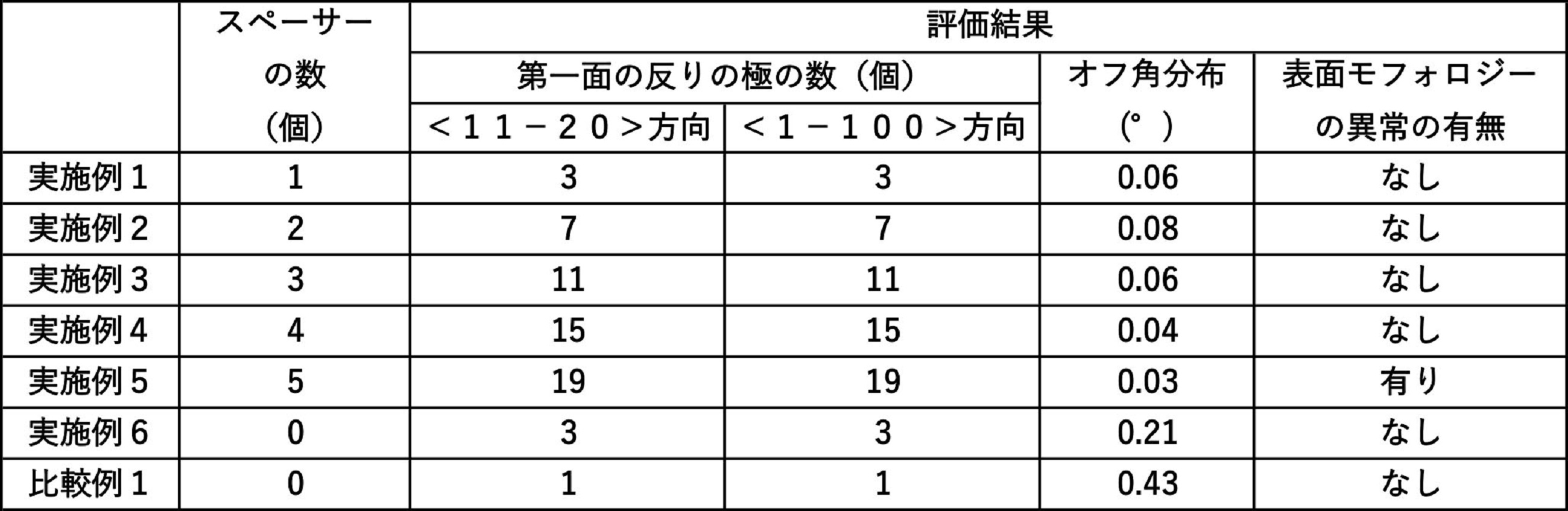
結果を表1に示した。
スペーサーの数を2個とし、2個のスペーサーの形状は、直径の異なる円形リング状(ドーナツ状)で、直径はそれぞれ35mm、85mm、リング幅は共通で10mm、2個のスペーサーは基板の中心を中心としてほぼ同心円に置き、2個のスペーサーがなす重心が基板の中心と一致するように配置した以外は、実施例1と同様に行い、窒化ガリウム自立基板としてのウエハー(2)を作製した。
ウエハー(2)の厚みは500μmであった。
得られた自立基板のGa極性面におけるオフ角を評価した。次いで、自立基板のGa極性面上に、MOCVD法によって、LED素子構造をエピタキシャル膜として成長させ、表面モフォロジーを評価した。
結果を表1に示した。
スペーサーの数を3個、3個のスペーサーの形状は、直径の異なる円形リング状(ドーナツ状)で、直径はそれぞれ23mm、56mm、90mm、リング幅は共通で6mm、3個のスペーサーは基板の中心を中心としてほぼ同心円に置き、3個のスペーサーがなす重心が基板の中心と一致するように配置した以外は、実施例1と同様に行い、窒化ガリウム自立基板としてのウエハー(3)を作製した。
ウエハー(3)の厚みは500μmであった。
得られた自立基板のGa極性面におけるオフ角を評価した。次いで、自立基板のGa極性面上に、MOCVD法によって、LED素子構造をエピタキシャル膜として成長させ、表面モフォロジーを評価した。
結果を表1に示した。
スペーサーの数を4個、4個のスペーサーの形状は、直径の異なる円形リング状(ドーナツ状)で、直径はそれぞれ17mm、42mm、67mm、92mm、リング幅は共通で5mm、4個のスペーサーは基板の中心を中心としてほぼ同心円に置き、4個のスペーサーがなす重心が基板の中心と一致するように配置した以外は、実施例1と同様に行い、窒化ガリウム自立基板としてのウエハー(4)を作製した。
ウエハー(4)の厚みは500μmであった。
得られた自立基板のGa極性面におけるオフ角を評価した。次いで、自立基板のGa極性面上に、MOCVD法によって、LED素子構造をエピタキシャル膜として成長させ、表面モフォロジーを評価した。
結果を表1に示した。
スペーサーの数を5個、5個のスペーサーの形状は、直径の異なる円形リング状(ドーナツ状)で、直径はそれぞれ14mm、34mm、54mm、74mm、94mm、リング幅は共通で4mm、5個のスペーサーは基板の中心を中心としてほぼ同心円に置き、5個のスペーサーがなす重心が基板の中心と一致するように配置した以外は、実施例1と同様に行い、窒化ガリウム自立基板としてのウエハー(5)を作製した。
ウエハー(5)の厚みは500μmであった。
得られた自立基板のGa極性面におけるオフ角を評価した。次いで、自立基板のGa極性面上に、MOCVD法によって、LED素子構造をエピタキシャル膜として成長させ、表面モフォロジーを評価した。
結果を表1に示した。
スペーサーを用いず、代わりに、表面を図7に示すような断面形状(L=25mm、H=0.03mm)に加工したセラミックス製の加工定盤(加工定盤の中心軸が軸60)を用いた以外は、実施例1と同様に行い、窒化ガリウム自立基板としてのウエハー(6)を作製した。
ウエハー(6)の厚みは500μmであった。
得られた自立基板のGa極性面におけるオフ角を評価した。次いで、自立基板のGa極性面上に、MOCVD法によって、LED素子構造をエピタキシャル膜として成長させ、表面モフォロジーを評価した。
結果を表1に示した。
スペーサーを用いず、加工定盤に貼り付ける際の圧力を0.01MPaとした以外は、実施例1と同様に行い、窒化ガリウム自立基板としてのウエハー(C1)を作製した。
ウエハー(C1)の厚みは500μmであった。
得られた自立基板のGa極性面におけるオフ角を評価した。次いで、自立基板のGa極性面上に、MOCVD法によって、LED素子構造をエピタキシャル膜として成長させ、表面モフォロジーを評価した。
結果を表1に示した。
スペーサーを用いなかった以外は、実施例1と同様に行ったところ、荷重を印加して加工定盤に貼り付ける際に基板にクラックが発生した。クラックが発生したため、以後の工程を中止した。
100’ 自立基板
1 下地基板
1a 下地基板1の主面
1b 下地基板1の裏面
2 種結晶膜
2a 種結晶膜2のIII族元素極性面
3 III族元素窒化物層
4 機能層
5 機能素子
10 主面
10’ 主面
20 裏面
20’ 裏面
30 側面
50 加工定盤
50’ 表面を加工した加工定盤
60 加工定盤の中心軸
70 c軸
80 基板表面で測定したオフ角δの、<11-20>方向(a軸方向)の成分δa、該<11-20>方向と直交する<1-100>方向(m軸方向)の成分δmのいずれかの一部
85 基板表面における法線
90 <11-20>方向もしくは<1-100>方向におけるオフ角の近似曲線の概略
Claims (6)
- 第一面と第二面とを備えるIII族元素窒化物半導体基板であって、
該第一面の結晶面の反りが複数の極を有する、
III族元素窒化物半導体基板。 - 前記第一面の結晶面の基板の中心を通る<11-20>方向の結晶面の反りと該<11-20>方向と直交する基板の中心を通る<1-100>方向の結晶面の反りが、いずれも複数の極を有する、請求項1に記載のIII族元素窒化物半導体基板。
- 前記極の数が3以上である、請求項1または2に記載のIII族元素窒化物半導体基板。
- 前記極において、隣接する極と極の間隔が3mm以上である、請求項1から3までのいずれかに記載のIII族元素窒化物半導体基板。
- 前記III族元素窒化物半導体基板全体のオフ角分布が0.40°以下である、請求項1から4までのいずれかに記載のIII族元素窒化物半導体基板。
- 前記III族元素窒化物半導体基板の直径が75mm以上である、請求項1から5までのいずれかに記載のIII族元素窒化物半導体基板。
Priority Applications (4)
| Application Number | Priority Date | Filing Date | Title |
|---|---|---|---|
| DE112021006806.7T DE112021006806B4 (de) | 2021-03-25 | 2021-11-19 | Halbleitersubstrat von einem Nitrid eines Elements der Gruppe III |
| CN202180093245.1A CN116997690A (zh) | 2021-03-25 | 2021-11-19 | Iii族元素氮化物半导体基板 |
| JP2023508455A JPWO2022201635A1 (ja) | 2021-03-25 | 2021-11-19 | |
| US18/451,934 US12685040B2 (en) | 2021-03-25 | 2023-08-18 | Group-III element nitride semiconductor substrate |
Applications Claiming Priority (2)
| Application Number | Priority Date | Filing Date | Title |
|---|---|---|---|
| JP2021-051046 | 2021-03-25 | ||
| JP2021051046 | 2021-03-25 |
Related Child Applications (1)
| Application Number | Title | Priority Date | Filing Date |
|---|---|---|---|
| US18/451,934 Continuation US12685040B2 (en) | 2021-03-25 | 2023-08-18 | Group-III element nitride semiconductor substrate |
Publications (1)
| Publication Number | Publication Date |
|---|---|
| WO2022201635A1 true WO2022201635A1 (ja) | 2022-09-29 |
Family
ID=83395497
Family Applications (1)
| Application Number | Title | Priority Date | Filing Date |
|---|---|---|---|
| PCT/JP2021/042574 Ceased WO2022201635A1 (ja) | 2021-03-25 | 2021-11-19 | Iii族元素窒化物半導体基板 |
Country Status (5)
| Country | Link |
|---|---|
| US (1) | US12685040B2 (ja) |
| JP (1) | JPWO2022201635A1 (ja) |
| CN (1) | CN116997690A (ja) |
| DE (1) | DE112021006806B4 (ja) |
| WO (1) | WO2022201635A1 (ja) |
Citations (3)
| Publication number | Priority date | Publication date | Assignee | Title |
|---|---|---|---|---|
| JP2005136167A (ja) * | 2003-10-30 | 2005-05-26 | Sumitomo Electric Ind Ltd | 窒化物半導体基板の製造方法と窒化物半導体基板 |
| JP2011009700A (ja) * | 2009-05-26 | 2011-01-13 | Hitachi Cable Ltd | 化合物半導体基板の製造方法 |
| JP2021008399A (ja) * | 2020-10-07 | 2021-01-28 | 三菱ケミカル株式会社 | GaN単結晶およびGaN単結晶製造方法 |
Family Cites Families (8)
| Publication number | Priority date | Publication date | Assignee | Title |
|---|---|---|---|---|
| TW417315B (en) | 1998-06-18 | 2001-01-01 | Sumitomo Electric Industries | GaN single crystal substrate and its manufacture method of the same |
| JP3788041B2 (ja) | 1998-06-30 | 2006-06-21 | 住友電気工業株式会社 | GaN単結晶基板の製造方法 |
| JP5244628B2 (ja) | 2009-01-21 | 2013-07-24 | 日本碍子株式会社 | 3b族窒化物結晶板の製法 |
| JP5212283B2 (ja) * | 2009-07-08 | 2013-06-19 | 日立電線株式会社 | Iii族窒化物半導体自立基板の製造方法、iii族窒化物半導体自立基板、iii族窒化物半導体デバイスの製造方法及びiii族窒化物半導体デバイス |
| JP6714431B2 (ja) * | 2016-05-27 | 2020-06-24 | 株式会社サイオクス | 結晶基板の製造方法 |
| JP6982469B2 (ja) * | 2017-10-27 | 2021-12-17 | 古河機械金属株式会社 | Iii族窒化物半導体基板及びiii族窒化物半導体基板の製造方法 |
| JP6697748B2 (ja) * | 2017-11-22 | 2020-05-27 | パナソニックIpマネジメント株式会社 | GaN基板およびその製造方法 |
| JP6595678B1 (ja) | 2018-08-29 | 2019-10-23 | 株式会社サイオクス | 窒化物半導体基板、窒化物半導体基板の製造方法および積層構造体 |
-
2021
- 2021-11-19 WO PCT/JP2021/042574 patent/WO2022201635A1/ja not_active Ceased
- 2021-11-19 CN CN202180093245.1A patent/CN116997690A/zh active Pending
- 2021-11-19 DE DE112021006806.7T patent/DE112021006806B4/de active Active
- 2021-11-19 JP JP2023508455A patent/JPWO2022201635A1/ja active Pending
-
2023
- 2023-08-18 US US18/451,934 patent/US12685040B2/en active Active
Patent Citations (3)
| Publication number | Priority date | Publication date | Assignee | Title |
|---|---|---|---|---|
| JP2005136167A (ja) * | 2003-10-30 | 2005-05-26 | Sumitomo Electric Ind Ltd | 窒化物半導体基板の製造方法と窒化物半導体基板 |
| JP2011009700A (ja) * | 2009-05-26 | 2011-01-13 | Hitachi Cable Ltd | 化合物半導体基板の製造方法 |
| JP2021008399A (ja) * | 2020-10-07 | 2021-01-28 | 三菱ケミカル株式会社 | GaN単結晶およびGaN単結晶製造方法 |
Also Published As
| Publication number | Publication date |
|---|---|
| US20230395373A1 (en) | 2023-12-07 |
| JPWO2022201635A1 (ja) | 2022-09-29 |
| DE112021006806B4 (de) | 2026-01-15 |
| DE112021006806T5 (de) | 2023-11-16 |
| CN116997690A (zh) | 2023-11-03 |
| US12685040B2 (en) | 2026-07-14 |
Similar Documents
| Publication | Publication Date | Title |
|---|---|---|
| US8404045B2 (en) | Method for manufacturing group III nitride single crystals | |
| JP4696935B2 (ja) | Iii−v族窒化物系半導体基板及びiii−v族窒化物系発光素子 | |
| CN115997050A (zh) | 大口径iii族氮化物系外延生长用基板及其制造方法 | |
| US20080290347A1 (en) | Gallium Nitride Semiconductor and Method of Manufacturing the Same | |
| US12564023B2 (en) | Free-standing substrate for epitaxial crystal growth, and functional element | |
| JP4333466B2 (ja) | 半導体基板の製造方法及び自立基板の製造方法 | |
| JP2009143778A (ja) | 窒化アルミニウム結晶の成長方法と窒化アルミニウム基板および半導体デバイス | |
| US20230352298A1 (en) | Group-iii element nitride semiconductor substrate | |
| CN118475733A (zh) | 高特性外延生长用基板及其制造方法 | |
| US12057307B2 (en) | Group-III element nitride semiconductor substrate | |
| US20230395373A1 (en) | Group-iii element nitride semiconductor substrate | |
| US7326477B2 (en) | Spinel boules, wafers, and methods for fabricating same | |
| JP2011216548A (ja) | GaN系半導体エピタキシャル基板の製造方法 | |
| WO2023157547A1 (ja) | Iii族元素窒化物半導体基板および貼り合わせ基板 | |
| US20250212478A1 (en) | Group-iii element nitride semiconductor substrate and bonded substrate | |
| US12550490B2 (en) | Group-III element nitride semiconductor substrate | |
| US20240379907A1 (en) | Group iii element nitride semiconductor substrate and bonded substrate | |
| WO2025196855A1 (ja) | Iii族元素窒化物基板、貼合せ基板、半導体素子およびiii族元素窒化物基板の製造方法 | |
| CN120712386A (zh) | Iii族元素氮化物基板及iii族元素氮化物基板的制造方法 |
Legal Events
| Date | Code | Title | Description |
|---|---|---|---|
| 121 | Ep: the epo has been informed by wipo that ep was designated in this application |
Ref document number: 21933233 Country of ref document: EP Kind code of ref document: A1 |
|
| WWE | Wipo information: entry into national phase |
Ref document number: 202180093245.1 Country of ref document: CN |
|
| WWE | Wipo information: entry into national phase |
Ref document number: 2023508455 Country of ref document: JP |
|
| WWE | Wipo information: entry into national phase |
Ref document number: 112021006806 Country of ref document: DE |
|
| 122 | Ep: pct application non-entry in european phase |
Ref document number: 21933233 Country of ref document: EP Kind code of ref document: A1 |
|
| WWG | Wipo information: grant in national office |
Ref document number: 112021006806 Country of ref document: DE |