WO2022201457A1 - 偏分波器 - Google Patents
偏分波器 Download PDFInfo
- Publication number
- WO2022201457A1 WO2022201457A1 PCT/JP2021/012654 JP2021012654W WO2022201457A1 WO 2022201457 A1 WO2022201457 A1 WO 2022201457A1 JP 2021012654 W JP2021012654 W JP 2021012654W WO 2022201457 A1 WO2022201457 A1 WO 2022201457A1
- Authority
- WO
- WIPO (PCT)
- Prior art keywords
- terminal
- orthogonal
- cross
- sectional shape
- common terminal
- Prior art date
- Legal status (The legal status is an assumption and is not a legal conclusion. Google has not performed a legal analysis and makes no representation as to the accuracy of the status listed.)
- Ceased
Links
Images




Classifications
-
- H—ELECTRICITY
- H01—ELECTRIC ELEMENTS
- H01P—WAVEGUIDES; RESONATORS, LINES, OR OTHER DEVICES OF THE WAVEGUIDE TYPE
- H01P1/00—Auxiliary devices
- H01P1/16—Auxiliary devices for mode selection, e.g. mode suppression or mode promotion; for mode conversion
Definitions
- the present invention relates to polarization/demultiplexers mainly used in the VHF band, UHF band, microwave band and millimeter wave band.
- a circuit for separating two orthogonal linearly polarized waves in two frequency bands is useful in satellite communication feed circuits.
- this polarization/demultiplexer one having one coaxial terminal and one orthogonal terminal is known.
- a common terminal that transmits two orthogonal linearly polarized waves of two frequency bands is provided, a coaxial terminal is provided on the opposite surface of the common terminal, and an orthogonal terminal is provided in a direction perpendicular to the coaxial terminal.
- the coaxial terminal is arranged on the same central axis as the common terminal, and the square cross-sectional shape of the common terminal has a transformation part where the square cross-sectional shape of the common terminal transforms into the rectangular cross-sectional shape of the coaxial terminal.
- the structure is symmetrical in the vicinity of the coaxial terminal.
- a transforming portion is provided outside the cross-section of the common terminal in which the shape of the short-circuit surface transforms into the rectangular cross-sectional shape of the orthogonal terminal.
- a polarization/demultiplexer has a common terminal consisting of a circular or square waveguide, a coaxial terminal consisting of a rectangular waveguide, and an orthogonal terminal consisting of a rectangular waveguide.
- the orthogonal terminal is arranged in the same direction as the common terminal and facing the common terminal, the orthogonal terminal is arranged in the direction orthogonal to the common terminal, the common terminal transmits two linearly polarized waves, and one of the two linearly polarized waves , one linearly polarized wave is transmitted through the coaxial terminal and the other linearly polarized wave is transmitted through the orthogonal terminal, and between the common terminal and the coaxial terminal is the cross-sectional shape of the common terminal
- the coaxial terminal has a first transforming portion in which the cross-sectional shape of the coaxial terminal changes stepwise, and the coaxial terminal is arranged offset from the central axis of the common terminal, and has an orthogonal terminal and a short-circuit surface facing the orthogonal terminal. Between them, there is
- FIG. 1 is a perspective view of a polarization/demultiplexer according to Embodiment 1;
- FIG. 2 is a top view of the polarization/demultiplexer according to Embodiment 1;
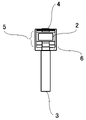
- FIG. 1 is a cross-sectional view of a polarization/demultiplexer according to Embodiment 1;
- FIG. 4 is a graph showing the reflection characteristics of orthogonal terminals in the low frequency band;
- FIG. 4 is a graph showing reflection characteristics of a coaxial terminal in a high frequency band; It is a figure which shows an example (straight line) of a metamorphic part. It is a figure which shows an example (circular arc shape) of a metamorphic part.
- FIG. 4 is a top view showing an example (straight line) of a transforming portion of a coaxial terminal or orthogonal terminal;
- FIG. 4 is a cross-sectional view showing an example (straight line) of a transforming portion of a coaxial terminal or orthogonal terminal;
- FIG. 4 is a top view showing an example (arcuate shape) of a metamorphic portion of a coaxial terminal or orthogonal terminal;
- FIG. 4 is a cross-sectional view showing an example (arcuate shape) of a metamorphic portion of a coaxial terminal or orthogonal terminal;
- FIG. 10 is a top view showing an example of a transforming section of a coaxial terminal or orthogonal terminal (a combination of a straight line and a stepped shape);
- FIG. 10 is a diagram showing a polarization/demultiplexer with a circular common terminal;
- FIG. 1 is a perspective view for explaining the configuration of a polarization/demultiplexer according to this embodiment.
- 1 is a common terminal
- 2 is a coaxial terminal
- 3 is an orthogonal terminal
- 4 is a short-circuit surface facing the orthogonal terminal
- 5 is a transforming portion of the coaxial terminal
- 6 is a transforming portion of the orthogonal terminal
- Reference numeral 7 denotes a transformer portion provided on one side of the short-circuit plane 4 facing the orthogonal terminals.
- the metamorphic section 5 is referred to as a first metamorphic section
- the metamorphic section 6 and the metamorphic section 7 are collectively referred to as a second metamorphic section.
- FIG. 2 is a top view for explaining the configuration of the polarization/demultiplexer according to this embodiment
- FIG. 3 is a cross-sectional view seen from the coaxial terminal side.
- the coaxial terminal 2 is arranged offset from the central axis of the common terminal 1 .
- the transformation portion 5 of the coaxial terminal 2 is provided so as to gradually transform the shape of the common terminal 1 into the shape of the coaxial terminal 2 .
- the transforming portion 6 of the orthogonal terminal 3 is provided inside the cross section of the common terminal 1 so that the cross-sectional shape is gradually transformed from the short-circuit surface 4 facing the orthogonal terminal 3 .
- the case is shown in which the transforming portion 7 provided on one side of the short-circuit surface 4 facing the orthogonal terminal 3 has a stepped shape.
- the wide wall dimension of the coaxial terminal 2 is smaller than the wide wall dimension of the orthogonal terminal 3 so that the coaxial terminal 2 transmits a higher frequency band than the orthogonal terminal 3. showing.
- the coaxial terminal 2 cuts off linearly polarized waves in the orthogonal direction, so that the coaxial terminal side is equivalently short-circuited. Therefore, when viewed from the top, it will act like a right angle bend.
- one side of the short-circuit surface 4 is provided with the stepped transformation portion 7, so that the linearly polarized wave can be smoothly transmitted.
- the orthogonal terminal 3 realizes good transmission characteristics and reflection characteristics.
- the size can be reduced compared to the conventional configuration in which the transforming portion is outside the cross section of the common terminal 1. Moreover, as already described, good reflection characteristics can be obtained at this time.
- FIG. 4 shows the reflection characteristics of the orthogonal terminal 3 in the low frequency band (Fl)
- FIG. 5 shows the reflection characteristics of the coaxial terminal 2 in the high frequency band (Fh).
- the horizontal axis indicates the values normalized by the center frequency of each frequency band (F/Fl, F/Fh), and the vertical axis indicates the reflection amplitude (S11 [dB]).
- 4 and 5 the solid lines are for the proposed configuration, and the dotted lines are for the conventional configuration.
- the coaxial terminal 2 of the proposed configuration has the same number of stages of the transformer section 5 of the coaxial terminal 2 of the conventional configuration, but the coaxial terminal 2 of the proposed configuration of the present embodiment is offset from the central axis of the common terminal 1.
- the orthogonal terminal 3 of the conventional configuration is not provided with a transformation portion
- the orthogonal terminal 3 of the proposed configuration is provided with a transformation portion inside the cross section of the common terminal 1
- one side of the short-circuit surface 4 facing the orthogonal terminal 3 is provided with a stepped metamorphic part 7 . Therefore, the proposed configuration and the conventional configuration are compared at the same size. As is clear from FIGS. 4 and 5, it has been confirmed that the proposed configuration does not deteriorate the reflection characteristics in the high frequency band as compared with the conventional configuration, and improves the reflection characteristics in the low frequency band.
- the coaxial terminal 2 has three stages of the transformer section 5 and the orthogonal terminal 3 has two stages of the transformer section 6 is shown. It's okay. Further, the wide wall dimension and the narrow wall dimension of the cross section of the metamorphic portion may be all the same, partly the same, or all different.
- the metamorphic portion 7 provided on one side of the short-circuit surface 4 may be linear as shown in FIG. In this case, since the shape is smoother than the stepped shape, there is an effect that better reflection characteristics can be obtained.
- the metamorphic portion 7 provided on one side of the short-circuit surface 4 may be arcuate as shown in FIG. In this case as well, the shape is smoother than the stepped shape, so there is an effect that better reflection characteristics can be obtained.
- the narrow wall dimension of the metamorphic portion 7 provided on one side of the short-circuit surface 4 is the same, but may be changed. In this case, there is an effect that the degree of freedom in design is further increased, and even better reflection characteristics are obtained.
- the transforming portion of the coaxial terminal 2 or orthogonal terminal 3 may be linear as shown in FIGS. In this case, there is an effect that the discontinuity is reduced and better reflection characteristics are obtained.
- the transforming portion of the coaxial terminal 2 or orthogonal terminal 3 may be curved as shown in FIGS. In this case, the discontinuity is reduced, the degree of freedom in design is increased, and an even better reflection characteristic is obtained.
Landscapes
- Control Of Motors That Do Not Use Commutators (AREA)
Abstract
円形または正方形の導波管からなる共通端子と、矩形導波管からなる共軸端子と、矩形導波管からなる直交端子を有し、共軸端子は、共通端子と同じ向きで共通端子と対向する面に配置され、直交端子は、共通端子と直交する向きに配置され、共通端子は、ふたつの直線偏波を伝送し、ふたつの直線偏波のうち、一方の直線偏波は共軸端子を伝送し、もう一方の直線偏波は直交端子を伝送する偏分波器であって、共通端子と共軸端子の間には、共通端子の断面形状から共軸端子の断面形状が段階的に変化する第1の変成部を有するとともに、共軸端子は、共通端子の中心軸からオフセットして配置され、直交端子と、直交端子と対向する短絡面の間には、短絡面の断面形状から直交端子の断面形状に段階的に変化する第2の変成部を有する偏分波器。
Description
この発明は、主としてVHF帯、UHF帯、マイクロ波帯およびミリ波帯で用いられる偏分波器に関するものである。
2つの周波数帯の直交する2つの直線偏波を分離するための回路(偏分波器)は衛星通信用給電回路で有用である。
この偏分波器としては、ひとつの共軸端子とひとつの直交端子を有するものが知られている。例えば、特許文献1では、2つの周波数帯の直交する2つの直線偏波を伝送する共通端子を有し、共通端子の対向面に共軸端子、共軸端子と直交する向きに直交端子を設けたものが示されている。
このような偏分波器では、共軸端子が共通端子と同じ中心軸上に配置されており、共通端子の正方形断面形状が共軸端子の矩形断面形状に変成していく変成部を有するため、共軸端子近傍では対称な構成となる。
また、直交端子と、直交端子と対向する短絡面の間には、短絡面の形状が直交端子の矩形断面形状に変成していく変成部が共通端子の断面よりも外側に設けられている。
このような偏分波器では、共軸端子が共通端子と同じ中心軸上に配置されており、共通端子の正方形断面形状が共軸端子の矩形断面形状に変成していく変成部を有するため、共軸端子近傍では対称な構成となる。
また、直交端子と、直交端子と対向する短絡面の間には、短絡面の形状が直交端子の矩形断面形状に変成していく変成部が共通端子の断面よりも外側に設けられている。
特許文献1で示される偏分波器において共通端子から入力されたひとつの周波数帯のひとつの直線偏波は共軸端子に出力される。このとき、共軸端子と共通端子は同じ中心軸上にあって対称な変成部が設けられており、かつ、直交端子の変成部は共通端子の断面から離れた位置にあるため、その影響は小さく、比較的良好な反射特性が得られる。
一方、共通端子から入力されたもう一方の周波数帯の直交する直線偏波は、直交端子に結合して出力される。このとき変成部が設けられているため比較的良好な反射特性が得られる。
一方、共通端子から入力されたもう一方の周波数帯の直交する直線偏波は、直交端子に結合して出力される。このとき変成部が設けられているため比較的良好な反射特性が得られる。
従来の偏分波器では、共軸端子と直交端子ともに変成部が設けられており比較的良好な反射特性が得られるものの、直交端子の変成部は共通端子の断面よりも外側に設けられているため大型化する問題がある。
また、直交端子の変成部を共通端子断面の内側になるように設けた場合、共軸端子に近接することになるため、その影響により、共軸端子の反射特性が劣化する問題がある。
この発明は、上記のような課題を解決するためになされたもので、共軸端子、直交端子ともに良好な反射特性が得られる小形な偏分波器を実現することを目的とするものである。
この発明による偏分波器は、円形または正方形の導波管からなる共通端子と、矩形導波管からなる共軸端子と、矩形導波管からなる直交端子を有し、共軸端子は、共通端子と同じ向きで共通端子と対向する面に配置され、直交端子は、共通端子と直交する向きに配置され、共通端子は、ふたつの直線偏波を伝送し、ふたつの直線偏波のうち、一方の直線偏波は共軸端子を伝送し、もう一方の直線偏波は直交端子を伝送する偏分波器であって、共通端子と共軸端子の間には、共通端子の断面形状から共軸端子の断面形状が段階的に変化する第1の変成部を有するとともに、共軸端子は、共通端子の中心軸からオフセットして配置され、直交端子と、直交端子と対向する短絡面の間には、短絡面の断面形状から直交端子の断面形状に段階的に変化する第2の変成部を有する。
本発明により、共軸端子、直交端子ともに良好な反射特性が得られる小形な偏分波器を実現することが可能となる。
実施の形態1
図1は本実施の形態に係わる偏分波器の構成を説明するための斜視図である。
図1において、1は共通端子、2は共軸端子、3は直交端子、4は直交端子3と対向する短絡面、5は共軸端子2の変成部、6は直交端子3の変成部、7は直交端子と対向する短絡面4の1辺に設けられた変成部である。
なお、変成部5を第1の変成部、変成部6と変成部7を合わせて第2の変成部と呼ぶ。
図1は本実施の形態に係わる偏分波器の構成を説明するための斜視図である。
図1において、1は共通端子、2は共軸端子、3は直交端子、4は直交端子3と対向する短絡面、5は共軸端子2の変成部、6は直交端子3の変成部、7は直交端子と対向する短絡面4の1辺に設けられた変成部である。
なお、変成部5を第1の変成部、変成部6と変成部7を合わせて第2の変成部と呼ぶ。
図2は本実施の形態に係わる偏分波器の構成を説明するための上面図、図3は共軸端子側から見た断面図である。図2に示されるように、共軸端子2は、共通端子1の中心軸からオフセットして配置されている。
共軸端子2の変成部5は、共通端子1から共軸端子2の形状に徐々に変成するように設けられている。また、直交端子3の変成部6は、共通端子1の断面の内側において、直交端子3と対向する短絡面4から断面形状が徐々に変成するように設けられている。
共軸端子2の変成部5は、共通端子1から共軸端子2の形状に徐々に変成するように設けられている。また、直交端子3の変成部6は、共通端子1の断面の内側において、直交端子3と対向する短絡面4から断面形状が徐々に変成するように設けられている。
さらに、直交端子3と対向する短絡面4の1辺に設けられた変成部7は、階段状である場合について示している。
なお、本実施の形態では、共軸端子2の方が、直交端子3よりも高い周波数帯を伝送するよう、共軸端子2の広壁面寸法が、直交端子3の広壁面寸法より小さい場合について示している。
なお、本実施の形態では、共軸端子2の方が、直交端子3よりも高い周波数帯を伝送するよう、共軸端子2の広壁面寸法が、直交端子3の広壁面寸法より小さい場合について示している。
次に動作について説明する。共通端子1から低い周波数帯のひとつの直線偏波が入力された場合、共軸端子2では直交する向きの直線偏波は遮断となるので、共軸端子側は等価的に短絡となる。このため、上面から見た場合は直角のベンドのように機能することになる。
このとき、短絡面4の1辺には階段状の変成部7が設けられているため、直線偏波の伝送がスムースになる。
さらに短絡面側から断面形状が徐々に変成して直交端子3の形状となるので、直交端子3において良好な通過特性、反射特性が実現される。
このとき、短絡面4の1辺には階段状の変成部7が設けられているため、直線偏波の伝送がスムースになる。
さらに短絡面側から断面形状が徐々に変成して直交端子3の形状となるので、直交端子3において良好な通過特性、反射特性が実現される。
一方、共通端子1から高い周波数帯のもう一方のひとつの直線偏波が入力された場合、直交端子3では直交する向きの直線偏波は遮断となるので、直交端子側は等価的には短絡となる。
このとき、直交端子3の変成部6が共軸端子2に近接しているためその影響が生じるものの、共軸端子2は共通端子1の中心軸からオフセットして配置されているため、共軸端子2の変成部5の影響が大きくなり、直交端子3の変成部6が近接する影響を相殺することが可能となる。
このため、共軸端子2において良好な通過特性、反射特性が実現される。
このとき、直交端子3の変成部6が共軸端子2に近接しているためその影響が生じるものの、共軸端子2は共通端子1の中心軸からオフセットして配置されているため、共軸端子2の変成部5の影響が大きくなり、直交端子3の変成部6が近接する影響を相殺することが可能となる。
このため、共軸端子2において良好な通過特性、反射特性が実現される。
本実施の形態の構成では、直交端子3の変成部6が共通端子1の断面の内側にあるため、変成部が共通端子1の断面の外側にある従来の構成に比べ小形できる効果がある。また、このとき良好な反射特性が得られることはすでに述べたとおりである。
ここで計算による本実施の形態における提案構成の効果を示す。
図4は低い周波数帯(Fl)の直交端子3の反射特性、図5は高い周波数帯(Fh)の共軸端子2の反射特性である。横軸はそれぞれの周波数帯の中心周波数で規格化したもの(F/Fl、F/Fh)であり、縦軸は反射振幅(S11[dB])を示している。
図4、図5において実線が提案構成、点線が従来構成によるものである。
提案構成における共軸端子2の変成部5と、従来構成における共軸端子の変成部の段数は同じであるが、本実施の形態提案構成の共軸端子2は共通端子1の中心軸からオフセットしている。また、従来構成の直交端子3には変成部を設けず、提案構成の直交端子3には共通端子1の断面の内側に変成部を設けるとともに、直交端子3と対向する短絡面4の1辺には階段状の変成部7を設けている。したがって、提案構成と従来構成は同じサイズでの比較となる。図4、5から明らかなように、提案構成では高い周波数帯の反射特性は従来構成と比べて劣化することなく、低い周波数の反射特性は向上していることを確認した。
図4は低い周波数帯(Fl)の直交端子3の反射特性、図5は高い周波数帯(Fh)の共軸端子2の反射特性である。横軸はそれぞれの周波数帯の中心周波数で規格化したもの(F/Fl、F/Fh)であり、縦軸は反射振幅(S11[dB])を示している。
図4、図5において実線が提案構成、点線が従来構成によるものである。
提案構成における共軸端子2の変成部5と、従来構成における共軸端子の変成部の段数は同じであるが、本実施の形態提案構成の共軸端子2は共通端子1の中心軸からオフセットしている。また、従来構成の直交端子3には変成部を設けず、提案構成の直交端子3には共通端子1の断面の内側に変成部を設けるとともに、直交端子3と対向する短絡面4の1辺には階段状の変成部7を設けている。したがって、提案構成と従来構成は同じサイズでの比較となる。図4、5から明らかなように、提案構成では高い周波数帯の反射特性は従来構成と比べて劣化することなく、低い周波数の反射特性は向上していることを確認した。
なお、従来構成において、共通端子1の断面の外側に直交端子3の変成部6を設けた場合は低い周波数帯において提案構成と同等の反射特性が見込まれるが、その場合は提案構成に比べ大型化する。したがって、提案構成において、従来構成と同等の反射特性を実現すればよい場合には小形化に利点がある。
なお、本実施の形態では、2つの周波数帯を分離する場合について示したが同じ周波数帯でもよい。
なお、ここでは、共軸端子2の変成部5は3段、直交端子3の変成部6は2段の場合について示したが、短絡面4の1辺における変成部7も含め、段数はいくつでもよい。さらに変成部における断面の広壁面寸法と狭壁面寸法は、それぞれすべて同じにしても、一部同じにしても、すべて異なるものとしてもよい。
なお、短絡面4の1辺に設けた変成部7は、図6に示すように直線状にしてもよい。この場合、階段状に比べ形状が滑らかになるのでより良好な反射特性が得られるという効果がある。
また、短絡面4の1辺に設けた変成部7は、図7に示すように円弧状にしてもよい。この場合も、階段状に比べ形状が滑らかになるのでより良好な反射特性が得られるという効果がある。
なお、図2、図6、図7では、短絡面4の1辺に設けた変成部7の狭壁面寸法は同じにしているが、変えてもよい。この場合、さらに設計の自由度があがり、さらに良好な反射特性が得られるという効果がある。
また、共軸端子2または直交端子3の変成部は、図8、9に示すように直線状にしてもよい。この場合、不連続が小さくなりさらに良好な反射特性が得られるという効果がある。
また、共軸端子2または直交端子3の変成部は、図10、11に示すように曲線状にしてもよい。この場合、不連続が小さくなるとともに設計の自由度があがり、さらに良好な反射特性が得られるという効果がある。
また、共軸端子2または直交端子3の変成部は、図12に示すように、直線状と階段状を組み合わせてもよい。この場合、設計の自由度が高くなり、さらに良好な反射特性が得られるという効果がある。
なお、直線状と曲線状の組み合わせ、曲線状と階段状の組み合わせなどでもよい。
なお、直線状と曲線状の組み合わせ、曲線状と階段状の組み合わせなどでもよい。
なお、加工方法としては、エンドミルを用いることを想定し、エンドミルの方向に応じた隅Rを設けてもよい。寸法の調整による隅Rの影響の補正は比較的容易である。
なお、加工方法としては、3Dプリンタを用いてもよい。曲線状などの加工は3Dプリンタを用いることにより、比較的容易である。
本実施の形態では、共通端子1が正方形の場合について示したが、図13に示すように共通端子1が円形でもよい。共軸端子2の変成部5は、円形から矩形に徐々に変成するようにすればよく、同様の効果が得られる。また、共通端子1を円形にした場合は、円形導波管端子を有する円偏波発生器との接続や、円形導波管端子を有するホーンアンテナとの接続が容易となるという利点もある。
1 共通端子、2 共軸端子、3 直交端子、4 短絡面、5 変成部、6 変成部、7 変成部。
Claims (11)
- 円形または正方形の導波管からなる共通端子と、
矩形導波管からなる共軸端子と、
矩形導波管からなる直交端子を有し、
前記共軸端子は、前記共通端子と同じ向きで前記共通端子と対向する面に配置され、前記直交端子は、前記共通端子と直交する向きに配置され、前記共通端子は、ふたつの直線偏波を伝送し、前記ふたつの直線偏波のうち、一方の直線偏波は前記共軸端子を伝送し、もう一方の直線偏波は直交端子を伝送する偏分波器であって、
前記共通端子と前記共軸端子の間には、前記共通端子の断面形状から前記共軸端子の断面形状が段階的に変化する第1の変成部を有するとともに、前記共軸端子は、前記共通端子の中心軸からオフセットして配置され、前記直交端子と、前記直交端子と対向する短絡面の間には、前記短絡面の断面形状から前記直交端子の断面形状に段階的に変化する第2の変成部を有する偏分波器。 - 前記短絡面の角は、階段状のコーナが設けられた請求項1に記載の偏分波器。
- 前記短絡面の角は、直線状のコーナが設けられた請求項1に記載の偏分波器。
- 前記短絡面の角は、円弧状のコーナが設けられた請求項1に記載の偏分波器。
- 前記第1の変成部は、その断面形状が階段状に変化する請求項1から4のいずれか一項に記載の偏分波器。
- 前記第1の変成部は、その断面形状が直線状に変化する請求項1から4のいずれか一項に記載の偏分波器。
- 前記第1の変成部は、その断面形状が曲線状に変化する請求項1から4のいずれか一項に記載の偏分波器。
- 前記第2の変成部は、その断面形状が階段状に変化する請求項1から7のいずれか一項に記載の偏分波器。
- 前記第2の変成部は、その断面形状が直線状に変化する請求項1から7のいずれか一項に記載の偏分波器。
- 前記第2の変成部は、その断面形状が曲線状に変化する請求項1から7のいずれか一項に記載の偏分波器。
- 前記第2の変成部は、前記共通端子の断面内に収まる請求項1から10のいずれか一項に記載の偏分波器。
Priority Applications (2)
| Application Number | Priority Date | Filing Date | Title |
|---|---|---|---|
| PCT/JP2021/012654 WO2022201457A1 (ja) | 2021-03-25 | 2021-03-25 | 偏分波器 |
| JP2023508339A JP7305079B2 (ja) | 2021-03-25 | 2021-03-25 | 偏分波器 |
Applications Claiming Priority (1)
| Application Number | Priority Date | Filing Date | Title |
|---|---|---|---|
| PCT/JP2021/012654 WO2022201457A1 (ja) | 2021-03-25 | 2021-03-25 | 偏分波器 |
Publications (1)
| Publication Number | Publication Date |
|---|---|
| WO2022201457A1 true WO2022201457A1 (ja) | 2022-09-29 |
Family
ID=83396603
Family Applications (1)
| Application Number | Title | Priority Date | Filing Date |
|---|---|---|---|
| PCT/JP2021/012654 Ceased WO2022201457A1 (ja) | 2021-03-25 | 2021-03-25 | 偏分波器 |
Country Status (2)
| Country | Link |
|---|---|
| JP (1) | JP7305079B2 (ja) |
| WO (1) | WO2022201457A1 (ja) |
Citations (4)
| Publication number | Priority date | Publication date | Assignee | Title |
|---|---|---|---|---|
| JPH0685502A (ja) * | 1992-08-31 | 1994-03-25 | Nec Corp | 直交偏分波器 |
| JP2013110456A (ja) * | 2011-11-17 | 2013-06-06 | Mitsubishi Electric Corp | 偏分波器 |
| CN203674349U (zh) * | 2013-11-15 | 2014-06-25 | 深圳国人通信股份有限公司 | 正交模变换器 |
| US20180343049A1 (en) * | 2017-05-26 | 2018-11-29 | Starry, Inc. | N-way polarization diversity for wireless access networks |
-
2021
- 2021-03-25 WO PCT/JP2021/012654 patent/WO2022201457A1/ja not_active Ceased
- 2021-03-25 JP JP2023508339A patent/JP7305079B2/ja active Active
Patent Citations (4)
| Publication number | Priority date | Publication date | Assignee | Title |
|---|---|---|---|---|
| JPH0685502A (ja) * | 1992-08-31 | 1994-03-25 | Nec Corp | 直交偏分波器 |
| JP2013110456A (ja) * | 2011-11-17 | 2013-06-06 | Mitsubishi Electric Corp | 偏分波器 |
| CN203674349U (zh) * | 2013-11-15 | 2014-06-25 | 深圳国人通信股份有限公司 | 正交模变换器 |
| US20180343049A1 (en) * | 2017-05-26 | 2018-11-29 | Starry, Inc. | N-way polarization diversity for wireless access networks |
Also Published As
| Publication number | Publication date |
|---|---|
| JP7305079B2 (ja) | 2023-07-07 |
| JPWO2022201457A1 (ja) | 2022-09-29 |
Similar Documents
| Publication | Publication Date | Title |
|---|---|---|
| US11569554B2 (en) | Orthomode transducer | |
| US7019603B2 (en) | Waveguide type ortho mode transducer | |
| US8461939B2 (en) | Waveguide orthomode transducer | |
| US10218076B1 (en) | Hexagonal waveguide based circularly polarized horn antennas | |
| EP2330681A1 (en) | Compact OMT device | |
| JP6463092B2 (ja) | デュアルバンド同軸アンテナフィードのためのマッチング及びパターン制御 | |
| EP3583661B1 (en) | Compact dual circular polarization multi-band waveguide feed network | |
| JP4035506B2 (ja) | 二重の円偏波を備えた周波数分離導波管モジュール | |
| EP1612880B1 (en) | Waveguide branching filter/polarizer | |
| US20190198963A1 (en) | Rf waveguide twist | |
| JP3908071B2 (ja) | ロータリージョイント | |
| US9653814B2 (en) | Mode generator device for a satellite antenna system and method for producing the same | |
| JP7305079B2 (ja) | 偏分波器 | |
| JP6865903B2 (ja) | 給電回路 | |
| EP4391216A1 (en) | Apparatus and system for splitting and combining signals in the frequency domain | |
| KR101491723B1 (ko) | 커플러를 이용한 이중 대역 피드혼 | |
| US20180366826A1 (en) | Phase shift circuit and power supply circuit | |
| EP4496116A1 (en) | Orthomode transducer and dual-linearly polarized feed source | |
| JP7496953B1 (ja) | 偏波分離回路およびアンテナ | |
| JPS6251801A (ja) | 直交偏波分波装置 | |
| JP4053928B2 (ja) | 円−矩形導波管変換器、直交偏波分離用分波器、一次放射器、給電部及びアンテナ | |
| WO2019111353A1 (ja) | 導波管方向性結合器及び偏波分離回路 | |
| KR101967302B1 (ko) | 전자기파의 수직/수평 편파 전환용 도파관 | |
| JP2000049503A (ja) | 円偏波発生器 |
Legal Events
| Date | Code | Title | Description |
|---|---|---|---|
| 121 | Ep: the epo has been informed by wipo that ep was designated in this application |
Ref document number: 21933063 Country of ref document: EP Kind code of ref document: A1 |
|
| ENP | Entry into the national phase |
Ref document number: 2023508339 Country of ref document: JP Kind code of ref document: A |
|
| NENP | Non-entry into the national phase |
Ref country code: DE |
|
| 122 | Ep: pct application non-entry in european phase |
Ref document number: 21933063 Country of ref document: EP Kind code of ref document: A1 |