WO2022190812A1 - 電子機器 - Google Patents
電子機器 Download PDFInfo
- Publication number
- WO2022190812A1 WO2022190812A1 PCT/JP2022/006541 JP2022006541W WO2022190812A1 WO 2022190812 A1 WO2022190812 A1 WO 2022190812A1 JP 2022006541 W JP2022006541 W JP 2022006541W WO 2022190812 A1 WO2022190812 A1 WO 2022190812A1
- Authority
- WO
- WIPO (PCT)
- Prior art keywords
- holder
- circuit board
- temporary locking
- temporary
- connector
- Prior art date
- Legal status (The legal status is an assumption and is not a legal conclusion. Google has not performed a legal analysis and makes no representation as to the accuracy of the status listed.)
- Ceased
Links
Images








Classifications
-
- H—ELECTRICITY
- H02—GENERATION; CONVERSION OR DISTRIBUTION OF ELECTRIC POWER
- H02G—INSTALLATION OF ELECTRIC CABLES OR LINES, OR OF COMBINED OPTICAL AND ELECTRIC CABLES OR LINES
- H02G3/00—Installations of electric cables or lines or protective tubing therefor in or on buildings, equivalent structures or vehicles
- H02G3/02—Details
- H02G3/08—Distribution boxes; Connection or junction boxes
- H02G3/16—Distribution boxes; Connection or junction boxes structurally associated with support for line-connecting terminals within the box
-
- B—PERFORMING OPERATIONS; TRANSPORTING
- B60—VEHICLES IN GENERAL
- B60R—VEHICLES, VEHICLE FITTINGS, OR VEHICLE PARTS, NOT OTHERWISE PROVIDED FOR
- B60R16/00—Electric or fluid circuits specially adapted for vehicles and not otherwise provided for; Arrangement of elements of electric or fluid circuits specially adapted for vehicles and not otherwise provided for
- B60R16/02—Electric or fluid circuits specially adapted for vehicles and not otherwise provided for; Arrangement of elements of electric or fluid circuits specially adapted for vehicles and not otherwise provided for electric constitutive elements
-
- H—ELECTRICITY
- H05—ELECTRIC TECHNIQUES NOT OTHERWISE PROVIDED FOR
- H05K—PRINTED CIRCUITS; CASINGS OR CONSTRUCTIONAL DETAILS OF ELECTRIC APPARATUS; MANUFACTURE OF ASSEMBLAGES OF ELECTRICAL COMPONENTS
- H05K7/00—Constructional details common to different types of electric apparatus
- H05K7/02—Arrangements of circuit components or wiring on supporting structure
- H05K7/12—Resilient or clamping means for holding component to structure
-
- B—PERFORMING OPERATIONS; TRANSPORTING
- B60—VEHICLES IN GENERAL
- B60R—VEHICLES, VEHICLE FITTINGS, OR VEHICLE PARTS, NOT OTHERWISE PROVIDED FOR
- B60R16/00—Electric or fluid circuits specially adapted for vehicles and not otherwise provided for; Arrangement of elements of electric or fluid circuits specially adapted for vehicles and not otherwise provided for
- B60R16/02—Electric or fluid circuits specially adapted for vehicles and not otherwise provided for; Arrangement of elements of electric or fluid circuits specially adapted for vehicles and not otherwise provided for electric constitutive elements
- B60R16/023—Electric or fluid circuits specially adapted for vehicles and not otherwise provided for; Arrangement of elements of electric or fluid circuits specially adapted for vehicles and not otherwise provided for electric constitutive elements for transmission of signals between vehicle parts or subsystems
- B60R16/0239—Electronic boxes
-
- Y—GENERAL TAGGING OF NEW TECHNOLOGICAL DEVELOPMENTS; GENERAL TAGGING OF CROSS-SECTIONAL TECHNOLOGIES SPANNING OVER SEVERAL SECTIONS OF THE IPC; TECHNICAL SUBJECTS COVERED BY FORMER USPC CROSS-REFERENCE ART COLLECTIONS [XRACs] AND DIGESTS
- Y02—TECHNOLOGIES OR APPLICATIONS FOR MITIGATION OR ADAPTATION AGAINST CLIMATE CHANGE
- Y02E—REDUCTION OF GREENHOUSE GAS [GHG] EMISSIONS, RELATED TO ENERGY GENERATION, TRANSMISSION OR DISTRIBUTION
- Y02E60/00—Enabling technologies; Technologies with a potential or indirect contribution to GHG emissions mitigation
- Y02E60/10—Energy storage using batteries
Definitions
- the technology disclosed in this specification relates to electronic equipment.
- a capacitor module that includes a resin holder that holds a plurality of capacitors and a wiring board that is fixed to the holder is known.
- the holder is provided with two board locking claws for fixing to the wiring board, and the board locking claws are engaged with through holes provided in the wiring board (see Patent Document 1).
- the component mounting area where the electronic components are mounted on the wiring board is distorted due to the pushing force when the board locking claw is pushed into the through hole, and cracks or the like occur in the connection portion of the electronic component to the wiring board. may occur.
- An electronic device disclosed in this specification includes a circuit board having one surface and the other surface opposite to the one surface; a holder engaging portion arranged on the one surface of the circuit board and engaged with the holder; and a temporary holder arranged on the other surface of the circuit board. and a fixing portion, wherein the holder extends from the holder body arranged on the one surface of the circuit board, and the holder extends from the holder body and is arranged on the other end of the circuit board opposite to the one end. and a temporary locking portion, wherein the temporary locking portion includes a temporary locking portion arranged on the other surface of the circuit board.
- the circuit board can be temporarily fixed to the holder while avoiding stress being applied to the circuit board.
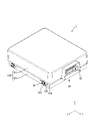
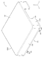
- FIG. 1 is a perspective view of an electronic device according to an embodiment
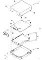
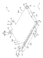
- FIG. FIG. 2 is an exploded perspective view of the electronic device of the embodiment.
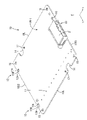
- FIG. 3 is a perspective view of a circuit board on which connectors are arranged.
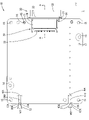
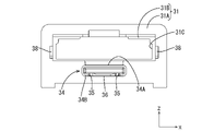
- FIG. 4 is a plan view showing a state in which the circuit board is temporarily locked by the holder and the connector cover.
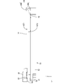
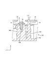
- 5 is a cross-sectional view taken along the line AA of FIG. 4.
- FIG. FIG. 6 is a rear view of the connector cover.
- FIG. 7 is a bottom view of the connector cover.
- FIG. 8 is a perspective view of the first holder.
- FIG. 9 is a perspective view of the second holder.
- FIG. 10 is a perspective view of the first outer case.
- FIG. 11 is a perspective view of the second outer case.
- FIG. 10 is a perspective view of the first outer case.
- FIG. 11 is a perspective view of the second outer case.
- FIG. 12 is a plan view showing a state in which the circuit board is assembled in the first holder.
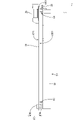
- FIG. 13 is a right side view showing a state in which the circuit board is attached to the first holder;
- FIG. 14 is a left side view showing a state in which the circuit board is attached to the first holder;
- FIG. 15 is a side view showing a state in which the capacitor is held by the first holder.
- FIG. 16 is a bottom view showing a state in which the capacitor is held by the first holder.
- FIG. 17 is a side view showing a state where the second holder is attached to the first holder.
- FIG. 18 is a side view showing a state in which the first outer case is assembled with the circuit board and the holder.
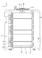
- FIG. 19 is a plan view showing a state where the first outer case is assembled with the circuit board and the holder.
- 20 is a cross-sectional view taken along line CC of FIG. 19.
- FIG. 19 is a cross-sectional view
- An electronic device disclosed in this specification includes a circuit board having one surface and the other surface opposite to the one surface; a fixing member arranged on one end of the circuit board, wherein the fixing member comprises a holder engaging portion arranged on the one surface of the circuit board and engaged with the holder, and a holder engaging portion arranged on the other surface of the circuit board.
- the holder includes a holder main body arranged on the one surface of the circuit board, and a holder main body extending from the holder main body to the other end opposite to the one end of the circuit board. and a temporary locking portion arranged on the circuit board, wherein the temporary locking portion comprises a temporary locking portion arranged on the other surface of the circuit board.
- the other end of the circuit board is held between the holder main body and the temporary fixing portion during assembly of the electronic device.
- the holder is engaged with the holder engaging portion of the fixing member, and one end of the circuit board is held between the holder engaging portion and the temporary fixing portion.
- the circuit board can be easily temporarily fixed to the holder while avoiding stress being applied to the circuit board.
- the circuit board may have a temporary locking recess that is disposed at the other end and receives the temporary locking portion. According to such a configuration, positional deviation between the circuit board and the holder can be suppressed, and the electronic device can be assembled smoothly.
- the holder includes a plurality of temporary locking portions having different widths
- the circuit board includes a plurality of temporary locking portions for receiving the plurality of temporary locking portions.
- the temporary locking recess is provided, and one temporary locking recess among the plurality of temporary locking recesses can accept one temporary locking portion among the plurality of temporary locking portions. However, it may have a width that does not permit the reception of other temporary locking portions.
- the circuit board has a boss hole arranged at the one end, and the holder is a boss inserted through the boss hole.
- the electronic equipment of (1) to (4) above may include a connector attached to the circuit board, and the fixing member may be a connector cover that covers at least part of the connector. According to such a configuration, the connector cover serves also as the temporary fixation of the circuit board, thereby suppressing an increase in the number of parts.
- the connector cover may include two temporary fixing portions arranged on both sides of the connector. According to such a configuration, positional deviation between the circuit board and the connector cover can be suppressed, and the electronic device can be assembled smoothly.
- the electronic device of (1) to (6) above includes an outer case covering the circuit board and the holder, wherein the outer case includes a board fixing portion to which only the circuit board is fixed, and only the holder. may be provided with a holder fixing portion to which is fixed.
- the circuit board and holder are separately fixed to the outer case.
- the circuit board and the holder can be firmly fixed to the outer case, respectively, as compared with the case where the circuit board and the holder are fixed together. It is possible to avoid applying a load to the connection part of the
- the electronic device 1 is a backup power supply device included in a shift-by-wire (SBW) device provided in a vehicle.
- SBW shift-by-wire
- SBW-ECU shift control unit
- the electronic device 1 includes a circuit board 10, a connector 20 fixed to the circuit board 10, a connector cover 30 (an example of a fixing member) covering the connector 20, and a It includes a holder 50 assembled to hold a capacitor 40 (an example of a storage element), and an outer case 100 housing the circuit board 10 and the holder 50 inside.
- the circuit board 10 is a printed board having a well-known configuration in which conductive paths are formed on one side or both sides of an insulating plate by printed wiring technology.
- the circuit board 10 has a rectangular plate shape as a whole, and has a first short side 10S1 and a second short side 10S2, two long sides 10L, a connector placement surface 10F1, and a connector placement surface. It has a holder arrangement surface 10F2 opposite to 10F1.
- the circuit board 10 includes a plurality of through holes 11, a first temporary locking recess 12 (an example of a temporary locking recess, one temporary locking recess), and a second temporary locking recess 13. (an example of a temporary locking recess), two relief recesses 14, four first screw insertion holes 15, a first boss hole 16 (an example of a boss hole), and two second boss holes 17. have.
- the first temporary locking recess 12 extends from the second short side 10S2 of the circuit board 10, and is composed of two parallel first side edges 12A and a first deep edge 12B connecting the two first side edges 12A.
- the second temporary locking recess 13 extends from the second short side 10S2 of the circuit board 10, and is composed of two second side edges 13A parallel to each other and a second deep edge 13B connecting the two second side edges 13A.
- the width W1 of the first temporary locking recess 12 defined by the distance between the two first side edges 12A is the width of the second temporary locking recess 12 defined by the distance between the two second side edges 13A. It is smaller than the width W2 of the locking recess 13 .
- Each of the two escape recesses 14 is a recess recessed inward from each of the two long sides 10L of the circuit board 10 .
- the four first screw insertion holes 15 are arranged at the four corners of the circuit board 10, respectively.
- the first boss hole 16 is arranged at one end of the circuit board 10 adjacent to the first short side 10S1.
- Each of the two second boss holes 17 is arranged adjacent to each of the two escape recesses 14 .
- the connector 20 is arranged on the connector placement surface 10F1 of the circuit board 10, as shown in FIGS.
- the connector 20 includes a connector housing 21 that can be fitted with a mating connector, and a plurality of terminal fittings 25 assembled to the connector housing 21 and connected to conductive paths of the circuit board 10 .
- the connector housing 21 is made of synthetic resin and has a terminal holding wall 22 and a hood portion 23 extending from the terminal holding wall 22 .
- the terminal holding wall 22 is a thick plate-like portion that holds the terminal fitting 25, as shown in FIG.
- the hood portion 23 has a rectangular tubular shape extending from the terminal holding wall 22 and has an opening (fitting opening 24 ) on the side opposite to the terminal holding wall 22 .
- the connector 20 is fixed with a portion adjacent to the fitting opening 24 protruding outward from the first short side 10S1 of the circuit board 10 .
- the connector cover 30 is attached to the connector 20 and is a waterproof member for preventing water from splashing on the fitting portion between the connector 20 and the mating connector. As shown in FIGS. 4, 5, 6 and 7, the connector cover 30 includes a back wall 31, a waterproof wall 32, a holder engaging portion 34, and two temporary fixing portions 38. .
- the back wall 31 includes a first back wall 31A and a block-shaped connector insertion portion 31B extending from the first back wall 31A. It has a connector entry hole 31C that penetrates through 31B and allows entry of a mating connector.
- the waterproof wall 32 is a U-shaped wall erected from the first rear wall 31A and surrounding the connector insertion portion 31B.
- the waterproof wall 32 has a fitting groove 33 on its outer surface, as shown in FIG.
- the fitting groove 33 is a groove extending over the entire length of the waterproof wall 32 .
- the holder engaging portion 34 is a rectangular tubular portion extending from the first back wall 31A in the direction opposite to the waterproof wall 32, as shown in FIGS.
- the holder engaging portion 34 has a first parallel wall 34A and a second parallel wall 34B that are parallel to each other.
- the second parallel wall 34B has two slits 35 parallel to each other, and the portion between the two slits 35 is connected to the back wall 31.
- the first flexible piece 36 has a locking hole 37 .
- Each of the two temporary fixing portions 38 is a plate piece projecting from the back wall 31 to the side opposite to the waterproof wall 32, as shown in FIGS.
- the two temporary fixing portions 38 are arranged on both sides of the connector entrance hole 31C, as shown in FIG.
- the capacitor 40 is, for example, an electric double layer capacitor, a lithium ion capacitor, or the like, and has a cylindrical capacitor body 41 and two lead terminals 42 extending from the capacitor body 41 .
- the holder 50 is made of synthetic resin, and, as shown in FIGS. and
- the first holder 51 includes a rectangular plate-like capacitor holding wall 56 , a first frame 52 (an example of a holder main body) extending from the periphery of the capacitor holding wall 56 , and a lead insertion portion 57 . I have.
- the first frame 52 has a rectangular frame shape that is one size smaller than the circuit board 10 as a whole, and includes a first long wall 52L1 and a second long wall 52L2 that are parallel to each other, and the first long wall 52L1 and the second long wall 52L2.
- 3 support protrusions 55 are provided.
- the lead insertion portion 57 is arranged inside the first frame 52 and has a plurality of lead insertion holes 57A through which the lead terminals 42 can be inserted.
- the first holder 51 has a locking receiving portion 58 that engages with the holder engaging portion 34 of the connector cover 30 .
- the lock receiving portion 58 has a plate-like shape extending outward from the first short wall 52S1, and is arranged on the holder placement surface 10F2 of the circuit board 10. , and a first locking claw 58B projecting from the locking receiving piece 58A.
- the first holder 51 includes a first support column 61 extending from the first support protrusion 53 and a first boss 65 (an example of a boss) extending from the first support column 61.
- the first support column 61 has a cylindrical shape, extends from the first support protrusion 53 toward the circuit board 10 , and abuts on the holder placement surface 10F2 of the circuit board 10 .
- the first boss 65 has a cylindrical shape with a diameter smaller than that of the first support column 61 , extends from the first support column 61 , and is inserted into the first boss hole 16 .
- the first holder 51 includes a second support column 62 extending from the second support protrusion 54 and a third support column 63 arranged adjacent to the third support protrusion 55.
- the second support column 62 has a U-shaped plate shape, extends from the first support protrusion 53 toward the circuit board 10 , and abuts on the holder placement surface 10F2 of the circuit board 10 .
- the third support column 63 has a half-pipe shape, one end of which is connected to the outer surface of the second short wall 52S2, and the other end of which abuts on the holder placement surface 10F2 of the circuit board 10. As shown in FIG.
- the first holder 51 includes a first temporary locking portion 66 (temporary locking portion, an example of one temporary locking portion) and a second temporary locking portion 67 (temporary locking portion, etc.). (an example of a temporary locking portion).
- the first temporary locking portion 66 has an L-shaped plate shape, and includes a plate-shaped first temporary locking piece 66A extending from the second support protrusion 54 and a first temporary locking piece 66A extending from the tip of the first temporary locking piece 66A. and a temporary fixing plate 66B (an example of a temporary fixing portion).
- the second temporary locking portion 67 has an L-shaped plate shape, and includes a plate-shaped second temporary locking piece 67A extending from the third support protrusion 55 and a second temporary locking piece 67A extending from the tip of the second temporary locking piece 67A. and a temporary fixing plate 67B (an example of a temporary fixing plate).
- the first temporary locking piece 66A is received in the first temporary locking recess 12 and the second temporary locking piece 67A is received in the second temporary locking recess 13 .
- the width W3 of the first temporary locking piece 66A defined by the distance between both side edges of the first temporary locking piece 66A is the second temporary locking piece defined by the distance between both side edges of the second temporary locking piece 67A. It is smaller than the width W4 of the stop piece 67A.
- the first holder 51 includes a plate-like first mounting portion 71, a second mounting portion 72, and a third mounting portion 73, as shown in FIG.
- the first mounting portion 71 extends outward from the first long wall 52L1.
- the second mounting portion 72 extends outward from the second long wall 52L2.
- Each of the first attachment portion 71 and the second attachment portion 72 has one third boss hole 74 and one second screw insertion hole 75 .
- the third mounting portion 73 extends outward from the first short wall 52S1.
- the third attachment portion 73 has a fourth support column 64 .
- the fourth support column 64 has a cylindrical shape, extends from the third attachment portion 73 toward the circuit board 10 , and abuts on the holder placement surface 10F2 of the circuit board 10 .
- the second holder 81 includes a second frame 82 and a plurality of capacitor holding portions 83, as shown in FIG.
- the second frame 82 has a rectangular frame shape having the same outer shape as the first frame 52, and includes two third long walls 82L that are parallel to each other and ends of the two third long walls 82L that are connected to each other. and three third short walls 82S.
- Each of the plurality of capacitor holding portions 83 has a half-pipe shape.
- a plurality of capacitor holding portions 83 are arranged side by side inside the second frame 82 .
- each capacitor body 41 is held between the capacitor holding wall 56 and one capacitor holding portion 83 .
- Each lead terminal 42 of the capacitor 40 held by the holder 50 is inserted through each lead insertion hole 57A and the through hole 11 and soldered to the conductive path of the circuit board 10 .
- the outer case 100 is a shield case made of metal and includes a first outer case 101 and a second outer case 121 .
- the first outer case 101 is a tray-shaped member capable of accommodating the holder 50 therein, and includes a rectangular plate-shaped bottom wall 102 and a first peripheral wall extending from the peripheral edge of the bottom wall 102.
- First peripheral wall 103 includes fourth long wall 103L1 and fifth long wall 103L2 extending from the two long sides of bottom wall 102, respectively, and fourth short wall 103S1 and fifth short wall 103S1 extending from the two short sides of bottom wall 102, respectively. wall 103S2.
- the first outer case 101 has four board fixing portions 104 for fixing the circuit board 10, two holder fixing portions 105 for fixing the holder 50, and four fixing portions for fixing the second outer case 121. It has a base 106 and four case supports 107 . Each of the four board fixing parts 104 is cylindrical and has a first screw hole 108 . The four board fixing portions 104 are arranged at the four corners of the first outer case 101, respectively. One end of each board fixing portion 104 protrudes from the first peripheral wall 103 to the side opposite to the bottom wall 102 and abuts on the holder placement surface 10F2 of the circuit board 10 .
- One of the two holder fixing portions 105 is arranged on the inner surface of the fourth long wall 103L1, and the other one is arranged on the inner surface of the fifth long wall 103L2.
- Each holder fixing portion 105 has a semi-cylindrical shape and has a second screw hole 109 .
- Each pedestal 106 is block-shaped and has a third screw hole 111 .
- Each of the four case support portions 107 has a striped shape and protrudes from the edge of each of the four pedestals 106 on the bottom wall 102 side.
- the first outer case 101 includes two prismatic fourth support protrusions 112 and two columnar second bosses 113 .
- One fourth support projection 112 is arranged adjacent to the holder fixing portion 105 on the inner surface of the fourth long wall 103L1, and the other fourth support projection 112 is arranged on the inner surface of the fifth long wall 103L2. It is arranged adjacent to the fixed part 105 .
- Each of the two second bosses 113 protrudes from each of the two fourth support protrusions 112 and is inserted into each of the second boss holes 17 .
- the first outer case 101 has a columnar fifth support column 114 .
- the fifth support column 114 protrudes from the fourth long wall 103L1 in the direction opposite to the bottom wall 102 and abuts on the holder arrangement surface 10F2 of the circuit board 10. As shown in FIG.
- the first outer case 101 has a strip-shaped support rib 115 that supports the connector cover 30 .
- the support ribs 115 are arranged on the outer surface of the fourth short wall 103S1 and support the first back wall 31A and the waterproof wall 32. As shown in FIG.
- the second outer case 121 is a member that covers the first outer case 101 and the circuit board 10, and as shown in FIG. and a peripheral wall 123 .
- the second peripheral wall 123 includes a sixth long wall 123L extending from each of the two long sides of the top wall 122, and a sixth short wall 123S1 and a seventh short wall 123S2 extending from each of the two short sides of the top wall 122. It is
- the sixth short wall 123S1 has a cover concave portion 124 for receiving the connector cover 30 therein.
- the second outer case 121 has a plurality of plate-shaped fixing pieces 125 .
- Two fixing pieces 125 extend from each of the two sixth long walls 123L.
- Each fixing piece 125 is arranged at a position corresponding to each pedestal 106 of the first outer case 101 and has a third screw insertion hole 126 .
- the connector 20 is fixed to the circuit board 10 by reflow soldering.
- the circuit board 10 is attached to the first holder 51 as shown in FIGS.
- the first temporary locking piece 66A enters the first temporary locking recess 12, and the second temporary locking piece 67A enters the second temporary locking recess 13.
- the circuit board 10 is assembled. is locked to the first holder 51 .
- the width W1 of the first temporary locking recess 12 is larger than the width W3 of the first temporary locking piece 66A but smaller than the width W4 of the second temporary locking piece 67A. permits the reception of the first temporary locking piece 66A, but does not permit the reception of the second temporary locking piece 67A (see FIG. 4). This prevents the circuit board 10 from being fixed to the first holder 51 in the wrong direction.
- the first boss 65 is inserted through the first boss hole 16 and one end of the circuit board 10 is positioned in the first holder 51 .
- the first frame 52 and the locking receiving portion 58 are arranged on the holder arrangement surface 10F2 of the circuit board 10, and the first supporting column 61, the second supporting column 62, the third supporting column 63 and the fourth support column 64 are in contact with the holder placement surface 10F2 of the circuit board 10 to support the circuit board 10 .
- the first temporary fixing plate 66B and the second temporary fixing plate 67B are arranged on the connector arrangement surface 10F1 of the circuit board 10, and the movement of the other end of the circuit board 10 away from the first frame 52 is restricted. be done.
- the connector cover 30 is attached to the first holder 51 to which the circuit board 10 is attached.
- the holder engagement portion 34 is arranged on the holder placement surface 10F2 of the circuit board 10, and the lock receiving piece 58A is inserted therein.
- the first flexible piece 36 rides on the first locking claw 58B and bends outward, and the first locking claw 58B enters the locking hole 37, the first flexible piece 36 is elastically restored and the first locking claw 58B is locked to the edge of the locking hole 37 (see also FIG. 16).
- two temporary fixing portions 38 are arranged on the connector placement surface 10F1 of the circuit board 10 to restrict the movement of the circuit board 10 away from the first frame 52 .
- the circuit board 10 is temporarily fixed by the first holder 51 and the connector cover 30 .
- the first temporary locking piece 66A enters the first temporary locking recess 12
- the second temporary locking piece 67A enters the second temporary locking recess 13
- the two temporary fixing portions 38 of the connector 20 Positional displacement of the circuit board 10 is restricted by being arranged on both sides and by the first bosses 65 entering the first boss holes 16 .
- the capacitor 40 is attached to the first holder 51 .
- the assembly of the circuit board 10, the first holder 51, and the connector cover 30 is placed in a position (shown in FIG. 15) in which the circuit board 10 is positioned below the first holder 51. Posture).
- the capacitor 40 is set in the first holder 51 from above.
- Each lead terminal 42 is inserted through the corresponding lead insertion hole 57A and through hole 11 .
- the circuit board 10 is temporarily fixed by the first holder 51 and the connector cover 30, and the circuit board 10 is secured by the first temporary fixing plate 66B, the second temporary fixing plate 67B, and the temporary fixing portion 38. Since movement in the direction away from the first frame 52 is restricted, the circuit board 10 is prevented from falling from the first holder 51 during the work of mounting the capacitor 40, and the work of mounting the capacitor 40 is facilitated. done.
- the second holder 81 is attached to the first holder 51 as shown in FIG.
- Capacitor body 41 is sandwiched and held between first holder 51 and second holder 81 .
- the lead terminal 42 of the capacitor 40 is connected to the conductive path of the circuit board 10 by soldering.
- FIGS. 18, 19, and 20 the circuit board 10 and the holder 50 are assembled to the first outer case 101.
- FIG. A holder 50 is housed inside the first outer case 101 .
- the circuit board 10 is positioned with respect to the first outer case 101 by inserting the second bosses 113 into the second boss holes 17 .
- the four board fixing portions 104 and the fifth support columns 114 are in contact with the holder arrangement surface 10F2 of the circuit board 10 to support the circuit board 10 . Further, each holder fixing portion 105 abuts on each first mounting portion 71 .
- each of the four screws B is inserted into each of the first screw insertion holes 15 and screwed into each of the four board fixing portions 104, thereby fixing the circuit board 10 to the first outer case 101. be done.
- the holder 50 is fixed to the first outer case 101 by inserting each of the other two screws B into each of the second screw insertion holes 75 and screwing them onto each of the holder fixing portions 105 . In this way, the circuit board 10 and the holder 50 are not screwed collectively to the first outer case 101, but the circuit board 10 and the holder 50 are separately screwed to the first outer case 101. be done.
- the circuit board 10 and the holder 50 are firmly fixed to the first outer case 101, so that the positional deviation of the circuit board 10 and the holder 50 with respect to the first outer case 101 is avoided. A load is avoided from being applied to the soldered portion with the circuit board 10. ⁇
- the second outer case 121 is assembled to the first outer case 101, as shown in FIG.
- the second outer case 121 is put on the first outer case 101 so that the ceiling wall 122 covers the circuit board 10 .
- the peripheral portion of the cover concave portion 124 is fitted inside the fitting groove 33 , and the connector cover 30 is arranged so that most of the waterproof wall 32 protrudes outside the outer case 100 .
- Each fixed piece 125 is arranged along each pedestal 106 and supported by the case support portion 107 .
- Each of the four screws B is inserted through each of the third screw insertion holes 126 and screwed to each of the bases 106 .
- the electronic device 1 includes the circuit board 10 having the holder placement surface 10F2 and the connector placement surface 10F1 opposite to the holder placement surface 10F2, and the holder 50 holding the capacitor 40. and a connector cover 30 assembled to the holder 50 and arranged at one end of the circuit board 10, the connector cover 30 being arranged on the holder arrangement surface 10F2 of the circuit board 10 and engaged with the holder 50.
- first frame 52 having a holder engagement portion 34 and a temporary fixing portion 38 arranged on the connector arrangement surface 10F1 of the circuit board 10, and having the holder 50 arranged on the holder arrangement surface 10F2 of the circuit board 10;
- a first temporary locking portion 66 and a second temporary locking portion 67 extending from the first frame 52 and arranged at the other end opposite to the one end of the circuit board 10 are provided.
- the stop portion 66 and the second temporary locking portion 67 are provided with a first temporary fixing plate 66B and a second temporary fixing plate 67B arranged on the connector arrangement surface 10F1 of the circuit board 10, respectively.
- the circuit board 10 when the electronic device 1 is assembled, the other end of the circuit board 10 is held between the first frame 52 and the first temporary fixing plate 66B and the second temporary fixing plate 67B.
- the holder 50 is engaged with the holder engaging portion 34 of the connector cover 30 , and one end of the circuit board 10 is held between the holder engaging portion 34 and the temporary fixing portion 38 .
- the circuit board 10 can be easily temporarily fixed to the holder 50 while avoiding stress being applied to the circuit board 10 .
- the circuit board 10 has a first temporary locking recess 12 arranged at the other end to receive the first temporary locking portion 66 and a second temporary locking recess 12 arranged at the other end to receive the second temporary locking portion 67 . 2 temporary locking recesses 13 .
- the first holder 51 includes a first temporary locking portion 66 and a second temporary locking portion 67 having different widths
- the circuit board 10 has the first temporary locking portion 66 and the second temporary locking portion 67 . It has a first temporary locking recess 12 and a second temporary locking recess 13 for receiving each of the portions 67 , and the first temporary locking recess 12 is capable of accepting the first temporary locking portion 66 . However, it has a width W1 that does not allow the reception of the second temporary locking portion 67 .
- the circuit board 10 has a first boss hole 16 arranged at one end, and the holder 50 has a first boss 65 inserted through the first boss hole 16 .
- the circuit board 10 has a first boss hole 16 arranged at one end, and the holder 50 has a first boss 65 inserted through the first boss hole 16 .
- the electronic device 1 includes a connector 20 attached to the circuit board 10, and the circuit board 10 is temporarily fixed by a connector cover 30 that covers at least a portion of the connector 20.
- the connector cover 30 also serves as a temporary fixation of the circuit board 10, thereby suppressing an increase in the number of parts.
- the connector cover 30 has two temporary fixing portions 38 arranged on both sides of the connector 20 . With such a configuration, positional deviation between the circuit board 10 and the connector cover 30 can be suppressed, and the electronic device 1 can be assembled smoothly.
- the electronic device 1 includes an outer case 100 covering the circuit board 10 and the holder 50.
- the outer case 100 includes a board fixing portion 104 to which only the circuit board 10 is fixed and a holder fixing portion to which only the holder 50 is fixed. 105.
- the circuit board 10 and the holder 50 are separately fixed to the outer case 100 .
- the circuit board 10 and the holder 50 are firmly fixed to the outer case 100 compared to the case where the circuit board 10 and the holder 50 are fixed together.
- 50 and the first outer case 101 are avoided, and a load is avoided from being applied to the soldered portions of the lead terminals 42 and the circuit board 10.
- the outer case 100 is a metal shield case, but the outer case may be a resin case that does not have a shield function.
- the fixing member was the connector cover 30, but the fixing member may be a member having a function other than the function of covering the connector, and a member having only the function of temporarily fixing the circuit board. It doesn't matter if it is.
Landscapes
- Engineering & Computer Science (AREA)
- Microelectronics & Electronic Packaging (AREA)
- Architecture (AREA)
- Civil Engineering (AREA)
- Structural Engineering (AREA)
- Mechanical Engineering (AREA)
- Mounting Of Printed Circuit Boards And The Like (AREA)
- Mounting Components In General For Electric Apparatus (AREA)
- Connection Or Junction Boxes (AREA)
- Details Of Connecting Devices For Male And Female Coupling (AREA)
Abstract
Description
(1)本明細書によって開示される電子機器は、一面と、前記一面とは反対側の他面とを有する回路基板と、蓄電素子を保持するホルダと、前記ホルダに組み付けられて、前記回路基板の一端部に配される固定部材と、を備え、前記固定部材が、前記回路基板の前記一面に配されて前記ホルダに係合するホルダ係合部と、前記回路基板の他面に配される仮固定部と、を備え、前記ホルダが、前記回路基板の前記一面に配されるホルダ本体と、前記ホルダ本体から延び、前記回路基板の前記一端部とは反対側の他端部に配される仮係止部とを備えており、前記仮係止部が、前記回路基板の他面に配される仮止め部を備える。
本明細書によって開示される技術の具体例を、以下に図面を参照しつつ説明する。なお、本発明はこれらの例示に限定されるものではなく、特許請求の範囲によって示され、特許請求の範囲と均等の意味および範囲内でのすべての変更が含まれることが意図される。
回路基板10は、図3および図5に示すように、絶縁板の片面または両面に、プリント配線技術により導電路が形成された周知の構成のプリント基板である。回路基板10は、全体として長方形の板状であって、第1短辺10S1および第2短辺10S2と、2つの長辺10Lとを有しているとともに、コネクタ配置面10F1と、コネクタ配置面10F1とは反対側のホルダ配置面10F2とを有している。
コネクタ20は、図3、図4および図5に示すように、回路基板10のコネクタ配置面10F1に配されている。コネクタ20は、相手コネクタと嵌合可能なコネクタハウジング21と、コネクタハウジング21に組み付けられて回路基板10の導電路と接続される複数の端子金具25とを備えている。
コネクタカバー30は、コネクタ20に組み付けられ、コネクタ20と相手コネクタとの嵌合部に水がかかることを防ぐための防水部材である。このコネクタカバー30は、図4、図5、図6および図7に示すように、背壁31と、防水壁32と、ホルダ係合部34と、2つの仮固定部38とを備えている。
キャパシタ40は、例えば電気二重層キャパシタ、リチウムイオンキャパシタ等であって、円柱状のキャパシタ本体41と、キャパシタ本体41から延びる2本のリード端子42とを有する。
ホルダ50は、合成樹脂製であって、図2および図17に示すように、回路基板10のホルダ配置面10F2に配置される第1ホルダ51と、第1ホルダ51に組み付けられる第2ホルダ81とを備えている。
アウタケース100は、金属製のシールドケースであって、第1アウタケース101と第2アウタケース121とを備えている。
次に、上記の電子機器1を組み立てる手順の一例を説明する。
以上のように本実施形態によれば、電子機器1は、ホルダ配置面10F2と、ホルダ配置面10F2とは反対側のコネクタ配置面10F1とを有する回路基板10と、キャパシタ40を保持するホルダ50と、ホルダ50に組み付けられて、回路基板10の一端部に配されるコネクタカバー30と、を備え、コネクタカバー30が、回路基板10のホルダ配置面10F2に配されてホルダ50に係合するホルダ係合部34と、回路基板10のコネクタ配置面10F1に配される仮固定部38と、を備え、ホルダ50が、回路基板10のホルダ配置面10F2に配される第1フレーム52と、第1フレーム52から延び、回路基板10の一端部とは反対側の他端部に配される第1仮係止部66および第2仮係止部67とを備えており、第1仮係止部66および第2仮係止部67が、回路基板10のコネクタ配置面10F1に配される第1仮止め板66Bおよび第2仮止め板67Bを備える。
(1)上記実施形態では、アウタケース100が金属製のシールドケースであったが、アウタケースがシールド機能を有しない樹脂製のケースであっても構わない。
(2)上記実施形態では、固定部材がコネクタカバー30であったが、固定部材は、コネクタを覆う機能以外の機能を有する部材であってもよく、回路基板を仮固定する機能のみを有する部材であっても構わない。
10:回路基板
10F1:コネクタ配置面(他面)
10F2:ホルダ配置面(一面)
10L:長辺
10S1:第1短辺
10S2:第2短辺
11:スルーホール
12:第1仮係止凹部(仮係止凹部、一の仮係止凹部)
12A:第1側縁
12B:第1奥縁
13:第2仮係止凹部(仮係止凹部)
13A:第2側縁
13B:第2奥縁
14:逃がし凹部
15:第1ねじ挿通孔
16:第1ボス孔(ボス孔)
17:第2ボス孔
20:コネクタ
21:コネクタハウジング
22:端子保持壁
23:フード部
24:嵌合口
25:端子金具
30:コネクタカバー(固定部材)
31:背壁
31A:第1背壁
31B:コネクタ挿通部
31C:コネクタ進入孔
32:防水壁
33:嵌合溝
34:ホルダ係合部
34A:第1平行壁
34B:第2平行壁
35:スリット
36:第1撓み片
37:係止孔
38:仮固定部
40:キャパシタ(蓄電素子)
41:キャパシタ本体
42:リード端子
50:ホルダ
51:第1ホルダ
52:第1フレーム(ホルダ本体)
52L1:第1長壁
52L2:第2長壁
52S1:第1短壁
52S2:第2短壁
53:第1支持突部
54:第2支持突部
55:第3支持突部
56:キャパシタ保持壁
57:リード挿通部
57A:リード挿通孔
58:係止受部
58A:係止受片
58B:第1係止爪
61:第1支持柱
62:第2支持柱
63:第3支持柱
64:第4支持柱
65:第1ボス(ボス)
66:第1仮係止部(仮係止部、一の仮係止部)
66A:第1仮係止片
66B:第1仮止め板(仮止め部)
67:第2仮係止部(仮係止部、一の仮係止部)
67A:第2仮係止片
67B:第2仮止め板(仮止め部)
71:第1取付部
72:第2取付部
73:第3取付部
74:第3ボス孔
75:第2ねじ挿通孔
81:第2ホルダ
82:第2フレーム
82L:第3長壁
82S:第3短壁
83:キャパシタ保持部
100:アウタケース
101:第1アウタケース
102:底壁
103:第1周壁
103L1:第4長壁
103L2:第5長壁
103S1:第4短壁
103S2:第5短壁
104:基板固定部
105:ホルダ固定部
106:台座
107:ケース支持部
108:第1ねじ穴
109:第2ねじ穴
111:第3ねじ穴
112:第4支持突部
113:第2ボス
114:第5支持柱
115:支持リブ
121:第2アウタケース
122:天壁
123:第2周壁
123L:第6長壁
123S1:第6短壁
123S2:第7短壁
124:カバー用凹部
125:固定片
126:第3ねじ挿通孔
W1:幅
W2:幅
W3:幅
W4:幅
Claims (7)
- 一面と、前記一面とは反対側の他面とを有する回路基板と、
蓄電素子を保持するホルダと、
前記ホルダに組み付けられて、前記回路基板の一端部に配される固定部材と、を備え、
前記固定部材が、前記回路基板の前記一面に配されて前記ホルダに係合するホルダ係合部と、前記回路基板の他面に配される仮固定部と、を備え、
前記ホルダが、前記回路基板の前記一面に配されるホルダ本体と、前記ホルダ本体から延び、前記回路基板の前記一端部とは反対側の他端部に配される仮係止部とを備えており、前記仮係止部が、前記回路基板の他面に配される仮止め部を備える、電子機器。 - 前記回路基板が、前記他端部に配され、前記仮係止部を受け入れる仮係止凹部を有している、請求項1に記載の電子機器。
- 前記ホルダが、幅の異なる複数の前記仮係止部を備えており、前記回路基板が、前記複数の前記仮係止部のそれぞれを受け入れる複数の前記仮係止凹部を有しており、
前記複数の仮係止凹部のうち一の仮係止凹部が、前記複数の仮係止部のうち一の仮係止部の受け入れを許容可能であるが、他の仮係止部の受け入れを許容不能な幅を有している、請求項2に記載の電子機器。 - 前記回路基板が、前記他端部に配されるボス孔を有し、
前記ホルダが、前記ボス孔に挿通されるボスを備える、請求項1から請求項3のいずれか1項に記載の電子機器。 - 前記回路基板に取り付けられたコネクタを備え、
前記固定部材が前記コネクタの少なくとも一部を覆うコネクタカバーである、請求項1から請求項4のいずれか1項に記載の電子機器。 - 前記コネクタカバーが、前記コネクタの両側に配される2つの前記仮固定部を備える、請求項5に記載の電子機器。
- 前記回路基板および前記ホルダを覆うアウタケースを備え、
前記アウタケースが、前記回路基板のみが固定される基板固定部と、前記ホルダのみが固定されるホルダ固定部とを備えている、請求項1から請求項6のいずれか1項に記載の電子機器。
Priority Applications (2)
| Application Number | Priority Date | Filing Date | Title |
|---|---|---|---|
| US18/548,409 US20240306334A1 (en) | 2021-03-09 | 2022-02-18 | Electronic device |
| CN202280018833.3A CN116965162A (zh) | 2021-03-09 | 2022-02-18 | 电子设备 |
Applications Claiming Priority (2)
| Application Number | Priority Date | Filing Date | Title |
|---|---|---|---|
| JP2021037412A JP7491242B2 (ja) | 2021-03-09 | 2021-03-09 | 電子機器 |
| JP2021-037412 | 2021-03-09 |
Publications (1)
| Publication Number | Publication Date |
|---|---|
| WO2022190812A1 true WO2022190812A1 (ja) | 2022-09-15 |
Family
ID=83227594
Family Applications (1)
| Application Number | Title | Priority Date | Filing Date |
|---|---|---|---|
| PCT/JP2022/006541 Ceased WO2022190812A1 (ja) | 2021-03-09 | 2022-02-18 | 電子機器 |
Country Status (4)
| Country | Link |
|---|---|
| US (1) | US20240306334A1 (ja) |
| JP (1) | JP7491242B2 (ja) |
| CN (1) | CN116965162A (ja) |
| WO (1) | WO2022190812A1 (ja) |
Citations (2)
| Publication number | Priority date | Publication date | Assignee | Title |
|---|---|---|---|---|
| JPS51157853U (ja) * | 1975-06-10 | 1976-12-15 | ||
| JP2014239095A (ja) * | 2013-06-06 | 2014-12-18 | 株式会社オートネットワーク技術研究所 | 補助電源装置及び電気接続箱 |
Family Cites Families (3)
| Publication number | Priority date | Publication date | Assignee | Title |
|---|---|---|---|---|
| DE59812848D1 (de) * | 1997-10-11 | 2005-07-14 | Conti Temic Microelectronic | Gehäuse zur Aufnahme elektronischer Bauelemente |
| JP6028718B2 (ja) * | 2013-11-11 | 2016-11-16 | 住友電装株式会社 | 電気接続箱 |
| JP6421601B2 (ja) * | 2015-01-08 | 2018-11-14 | 株式会社オートネットワーク技術研究所 | キャパシタモジュール |
-
2021
- 2021-03-09 JP JP2021037412A patent/JP7491242B2/ja active Active
-
2022
- 2022-02-18 CN CN202280018833.3A patent/CN116965162A/zh active Pending
- 2022-02-18 US US18/548,409 patent/US20240306334A1/en not_active Abandoned
- 2022-02-18 WO PCT/JP2022/006541 patent/WO2022190812A1/ja not_active Ceased
Patent Citations (2)
| Publication number | Priority date | Publication date | Assignee | Title |
|---|---|---|---|---|
| JPS51157853U (ja) * | 1975-06-10 | 1976-12-15 | ||
| JP2014239095A (ja) * | 2013-06-06 | 2014-12-18 | 株式会社オートネットワーク技術研究所 | 補助電源装置及び電気接続箱 |
Also Published As
| Publication number | Publication date |
|---|---|
| CN116965162A (zh) | 2023-10-27 |
| JP2022137757A (ja) | 2022-09-22 |
| JP7491242B2 (ja) | 2024-05-28 |
| US20240306334A1 (en) | 2024-09-12 |
Similar Documents
| Publication | Publication Date | Title |
|---|---|---|
| EP3313157B1 (en) | Waterproof electronic control device | |
| CN109980401B (zh) | 电源分配箱的公差吸收结构和车辆电路体 | |
| US11431123B2 (en) | Connector having holding member for holding conductive member | |
| US10238012B2 (en) | Waterproof component-suppressing electronic control device | |
| CN110301021B (zh) | 蓄电单元 | |
| JP4756716B2 (ja) | コネクタ及び電子装置 | |
| US20170164488A1 (en) | Electrical junction box | |
| US7883351B2 (en) | Socket for mounting electronic component | |
| JP2001211527A (ja) | 電気接続箱 | |
| JP6211030B2 (ja) | 電子制御装置および電子制御装置の製造方法 | |
| WO2022190812A1 (ja) | 電子機器 | |
| US6827606B2 (en) | Connector with mounting ribs for mounting to a circuit board | |
| WO2015098482A1 (ja) | 電気回路装置 | |
| JP2583978Y2 (ja) | 回路基板の収納ハウジングの構造 | |
| JP2019149906A (ja) | 電気接続箱 | |
| CN111293650B (zh) | 电气连接箱 | |
| JP2001326480A (ja) | 基板収容体 | |
| JP2020173174A (ja) | バッテリー状態検知装置 | |
| JP2006148011A (ja) | 基板に対する電気素子の取付構造 | |
| US11971453B2 (en) | Battery state detection device | |
| TW200536191A (en) | Socket for electronic module | |
| US10874017B2 (en) | Board unit | |
| JP3362111B2 (ja) | 電気接続箱 | |
| JP4327033B2 (ja) | 電子制御装置の筐体構造 | |
| WO2024201572A1 (ja) | キャパシタモジュール,電源ユニット,キャパシタホルダ |
Legal Events
| Date | Code | Title | Description |
|---|---|---|---|
| 121 | Ep: the epo has been informed by wipo that ep was designated in this application |
Ref document number: 22766775 Country of ref document: EP Kind code of ref document: A1 |
|
| WWE | Wipo information: entry into national phase |
Ref document number: 18548409 Country of ref document: US |
|
| WWE | Wipo information: entry into national phase |
Ref document number: 202280018833.3 Country of ref document: CN |
|
| NENP | Non-entry into the national phase |
Ref country code: DE |
|
| 122 | Ep: pct application non-entry in european phase |
Ref document number: 22766775 Country of ref document: EP Kind code of ref document: A1 |