WO2022190352A1 - 半導体装置 - Google Patents
半導体装置 Download PDFInfo
- Publication number
- WO2022190352A1 WO2022190352A1 PCT/JP2021/010039 JP2021010039W WO2022190352A1 WO 2022190352 A1 WO2022190352 A1 WO 2022190352A1 JP 2021010039 W JP2021010039 W JP 2021010039W WO 2022190352 A1 WO2022190352 A1 WO 2022190352A1
- Authority
- WO
- WIPO (PCT)
- Prior art keywords
- layer
- semiconductor layer
- element region
- semiconductor
- isolation
- Prior art date
- Legal status (The legal status is an assumption and is not a legal conclusion. Google has not performed a legal analysis and makes no representation as to the accuracy of the status listed.)
- Ceased
Links
Images






Classifications
-
- G—PHYSICS
- G02—OPTICS
- G02F—OPTICAL DEVICES OR ARRANGEMENTS FOR THE CONTROL OF LIGHT BY MODIFICATION OF THE OPTICAL PROPERTIES OF THE MEDIA OF THE ELEMENTS INVOLVED THEREIN; NON-LINEAR OPTICS; FREQUENCY-CHANGING OF LIGHT; OPTICAL LOGIC ELEMENTS; OPTICAL ANALOGUE/DIGITAL CONVERTERS
- G02F1/00—Devices or arrangements for the control of the intensity, colour, phase, polarisation or direction of light arriving from an independent light source, e.g. switching, gating or modulating; Non-linear optics
- G02F1/01—Devices or arrangements for the control of the intensity, colour, phase, polarisation or direction of light arriving from an independent light source, e.g. switching, gating or modulating; Non-linear optics for the control of the intensity, phase, polarisation or colour
- G02F1/015—Devices or arrangements for the control of the intensity, colour, phase, polarisation or direction of light arriving from an independent light source, e.g. switching, gating or modulating; Non-linear optics for the control of the intensity, phase, polarisation or colour based on semiconductor elements having potential barriers, e.g. having a PN or PIN junction
- G02F1/017—Structures with periodic or quasi periodic potential variation, e.g. superlattices, quantum wells
-
- H—ELECTRICITY
- H01—ELECTRIC ELEMENTS
- H01S—DEVICES USING THE PROCESS OF LIGHT AMPLIFICATION BY STIMULATED EMISSION OF RADIATION [LASER] TO AMPLIFY OR GENERATE LIGHT; DEVICES USING STIMULATED EMISSION OF ELECTROMAGNETIC RADIATION IN WAVE RANGES OTHER THAN OPTICAL
- H01S5/00—Semiconductor lasers
- H01S5/02—Structural details or components not essential to laser action
- H01S5/026—Monolithically integrated components, e.g. waveguides, monitoring photo-detectors, drivers
Definitions
- the present invention relates to a semiconductor device having an active layer for forming an optical device.
- optical communication devices are classified according to the communication distance according to the application, but their basic configuration consists of a semiconductor laser that produces light as a carrier wave, an optical modulator that modulates the carrier wave, and an intensity of the modulated light. and an optical receiver for converting the modulated light into an electrical signal.
- optical communication devices are monolithically integrated on the same semiconductor substrate for the purpose of downsizing and improving power efficiency, depending on the application.
- differential modulation drive is required for the purpose of improving the S/N ratio of optical waveforms by increasing the use efficiency of modulation voltage and suppressing common mode noise.
- a conventional semiconductor optical modulator integrated laser used as an optical communication device monolithically integrates a laser and an optical modulator on the same substrate, and the GND of the device is connected to a common semiconductor layer.
- the differential modulation operation of the optical modulator section cannot be realized due to the following reasons. Since the GND between the laser and the optical modulator is short-circuited, when the optical modulator is operated for differential modulation, a single-phase modulation voltage flows into the laser, making it difficult to supply a desired voltage to the optical modulator. At the same time, an unnecessary voltage is supplied to the laser, which makes it difficult to operate the laser stably.
- a semi-insulating (SI) substrate is used, and the drive terminal of the device is open to GND.
- SI semi-insulating
- a p-polar semiconductor layer is formed on an SI substrate, an active layer is formed thereon, and an n-polar semiconductor layer is formed thereon.
- a p-polar semiconductor layer, a semi-insulating semiconductor layer, and a p-polar semiconductor layer are formed side by side on an SI substrate, an active layer is formed thereon, and an n-polar semiconductor layer is formed thereon. It is conceivable to integrate a laser and an optical modulator by a butt-joint process of forming a semiconductor layer.
- the present invention has been made to solve the above-described problems, and it is possible to maintain the crystal quality of each element in a state in which a plurality of elements having different functions are electrically separated from each other. It aims at monolithic integration.
- a semiconductor device is arranged between a substrate made of a semi-insulating III-V compound semiconductor, a first element region, a second element region, and between the first element region and the second element region.
- III a first active layer formed on the first semiconductor layer in the first element region and formed of a -V group compound semiconductor; and a first semiconductor formed of a III-V group compound semiconductor in the second element region a second active layer formed on the layer; and a semi-insulating group III-V compound semiconductor.
- the activation rate of carbon doped in the first semiconductor layer of is lower than the activation rate of carbon doped in the first semiconductor layers of the first element region and the second element region.
- the activation rate of carbon doped in the first semiconductor layer in the isolation region is Since the activation rate is lower than that of the carbon doped in the first semiconductor layer of the first element region and the second element region, a plurality of elements having different functions are electrically separated from each other. Monolithic integration is possible while maintaining the crystal quality of each element.
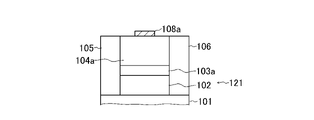
- FIG. 1 is a cross-sectional view showing the configuration of a semiconductor device according to Embodiment 1 of the present invention.
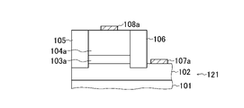
- FIG. 2A is a cross-sectional view showing the configuration of the semiconductor device according to Embodiment 1 of the present invention.
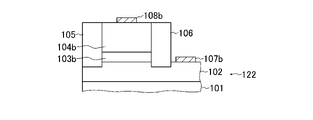
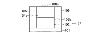
- FIG. 2B is a cross-sectional view showing the configuration of the semiconductor device according to Embodiment 1 of the present invention.
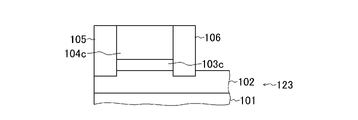
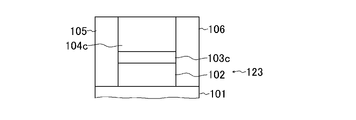
- FIG. 2C is a cross-sectional view showing the configuration of the semiconductor device according to Embodiment 1 of the present invention.
- FIG. 3 is a characteristic diagram showing the relationship between the resistance A of the first semiconductor layer 102 and the cross-sectional area of the first semiconductor layer 102 in the first element region 121 and the second element region 122 for each length of the isolation region 123. be.
- FIG. 3 is a characteristic diagram showing the relationship between the resistance A of the first semiconductor layer 102 and the cross-sectional area of the first semiconductor layer 102 in the first element region 121 and the second element region 122 for each length of the isolation region
- FIG. 4A is a cross-sectional view showing another configuration of the semiconductor device according to Embodiment 1 of the present invention.
- FIG. 4B is a cross-sectional view showing another configuration of the semiconductor device according to Embodiment 1 of the present invention.
- 4C is a cross-sectional view showing another configuration of the semiconductor device according to Embodiment 1 of the present invention.
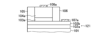
- FIG. FIG. 5A is a cross-sectional view showing the configuration of a semiconductor device according to Embodiment 2 of the present invention.
- FIG. 5B is a cross-sectional view showing the configuration of a semiconductor device according to Embodiment 2 of the present invention.
- FIG. 6 is a characteristic diagram showing the relationship between the resistance of the isolation region 123 and the length of the isolation region 123. As shown in FIG.
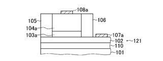
- FIG. 7A is a cross-sectional view showing the configuration of a semiconductor device according to Embodiment 3 of the present invention.
- FIG. 7B is a cross-sectional view showing the configuration of a semiconductor device according to Embodiment 3 of the present invention.
- FIG. 7C is a cross-sectional view showing the configuration of a semiconductor device according to Embodiment 3 of the present invention.
- FIG. 7D is a cross-sectional view showing the configuration of a semiconductor device according to Embodiment 3 of the present invention.
- FIG. 8 is a cross-sectional view showing the configuration of another semiconductor device according to the embodiment of the invention.
- Embodiment 1 First, a semiconductor device according to Embodiment 1 of the present invention will be described with reference to FIGS. 1, 2A, 2B, and 2C.
- This semiconductor device is composed of a substrate 101 made of a semi-insulating Group III-V compound semiconductor and a Group III-V compound semiconductor doped with carbon (C). and a first semiconductor layer 102 .
- the first semiconductor layer 102 can be made of any one of InGaAsP, InGaAs, InGaAlAs, and InAlAs.
- the first semiconductor layer 102 includes a first element region 121 , a second element region 122 , and is arranged between the first element region 121 and the second element region 122 to form the first element region 121 and the second element region 122 .
- has an isolation region 123 that separates the The first semiconductor layer 102 is integrally formed over the first element region 121 , the isolation region 123 and the second element region 122 .
- the activation rate of C doped in the first semiconductor layer 102 in the isolation region 123 is is made lower. Therefore, the first semiconductor layer 102 in the isolation region 123 has a higher resistance than the first element region 121 and the second element region 122 .
- the activation rate of C doped in the first semiconductor layer 102 in the isolation region 123 is set within a range where electrical isolation can be realized between the first element region 121 and the second element region 122 .
- this semiconductor device is composed of a III-V compound semiconductor, and is composed of a first active layer 103a formed on the first semiconductor layer 102 in the first element region 121 and a III-V compound semiconductor. and a second active layer 103 b formed on the first semiconductor layer 102 in the second element region 122 . Also, on the first semiconductor layer 102 in the isolation region 123, a first isolation layer 103c made of a semi-insulating III-V group compound semiconductor is provided on the first semiconductor layer 102 in the isolation region 123. The first separation layer 103c is sandwiched between the first active layer 103a and the second active layer 103b.
- the first active layer 103a, the first isolation layer 103c, and the second active layer 103b are individually formed. Also, the first active layer 103a, the first isolation layer 103c, and the second active layer 103b are formed to have the same thickness. Note that the same thickness means substantially the same thickness, and includes, for example, a difference of 10 nm from each other due to manufacturing restrictions. It is important that the thicknesses of the first active layer 103a, the first separation layer 103c, and the second active layer 103b are set so that the optical coupling efficiency of the optical waveguide between the respective parts is sufficiently high. is.
- this semiconductor device is composed of an n-type III-V group compound semiconductor, and includes a first n-type semiconductor layer 104a formed on a first active layer 103a and an n-type III-V group compound semiconductor. and a second n-type semiconductor layer 104b formed on the second active layer 103b.
- a second isolation layer 104c made of a semi-insulating III-V group compound semiconductor is provided on the first isolation layer 103c. The second isolation layer 104c is formed sandwiched between the first n-type semiconductor layer 104a and the second n-type semiconductor layer 104b.
- the first n-type semiconductor layer 104a, the second separation layer 104c, and the second n-type semiconductor layer 104b are formed individually (separately).
- the first n-type semiconductor layer 104a and the second n-type semiconductor layer 104b can be formed from the same layer.
- the first n-type semiconductor layer 104a, the second isolation layer 104c, and the second n-type semiconductor layer 104b are formed to have the same thickness.
- the same thickness means substantially the same thickness, and includes, for example, a difference of 10 nm from each other due to manufacturing restrictions. Moreover, they do not need to have the same thickness. For example, even if the second isolation layer 104c is 100 nm thicker than the first n-type semiconductor layer 104a, there is no effect on the characteristics.
- the first element region 121 is a laser and the second element region 122 is an optical modulator.
- This optical communication device has, for example, a first active layer 103a, a first separation layer 103c, and a second active layer 103b as cores, and has an optical waveguide structure whose arrangement direction is the waveguide direction.
- FIG. 1 shows a cross section parallel to this waveguide direction.
- FIG. 2A shows a cross section perpendicular to the waveguide direction in the first element region 121 .
- FIG. 2B shows a cross section perpendicular to the waveguide direction in the second element region 122 .
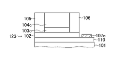
- FIG. 2C shows a cross section perpendicular to the waveguide direction in the isolation region 123 .
- the side surface of 104b in the waveguide direction is sandwiched (embedded) between the first SI layer 105 and the second SI layer 106 made of a semi-insulating semiconductor. This is the well-known buried heterostructure structure.
- a first SI layer 105 and a second SI layer 106 are formed on the first semiconductor layer 102 .
- a first p-electrode 107a is formed on the first semiconductor layer 102 in a region where the first SI layer 105 and the second SI layer 106 are not formed. It is also, in the first element region 121, a first n-electrode 108a is formed on the first n-type semiconductor layer 104a for ohmic connection to the first n-type semiconductor layer 104a.
- a second p-electrode 107b is formed on the first semiconductor layer 102 in a region where the first SI layer 105 and the second SI layer 106 are not formed. It is In the second element region 122, a second n-electrode 108b is formed on the second n-type semiconductor layer 104b for ohmic connection to the second n-type semiconductor layer 104b.
- the first SI layer 105 and the second SI layer 106 are formed so as to partly enter the first semiconductor layer 102 in the thickness direction. Note that the first SI layer 105 and the second SI layer 106 can also be formed without partially encroaching on the first semiconductor layer 102 in the thickness direction.
- the first semiconductor layer 102 is composed of one layer
- the first active layer 103a, the first separation layer 103c, and the second active layer 103b can be formed by a so-called butt joint process.
- the flatness of layer 103a, first separation layer 103c, and second active layer 103b is not impaired. Therefore, the optical waveguide formed by the first active layer 103a, the first separation layer 103c, and the second active layer 103b does not cause waveguide loss at each joint portion.
- Embodiment 1 a plurality of elements having different functions can be monolithically integrated while maintaining the crystal quality of each element in a state where the elements are electrically isolated from each other. .
- the first embodiment it is possible to realize differential modulation driving of monolithically integrated optical elements.
- the effects of the realization of differential modulation driving are, firstly, that the modulation amplitude voltage can be halved, and secondly, that the S/N of the optical signal can be improved due to the reduction of common mode noise (reference document 1).
- C has a smaller diffusion coefficient in semiconductors than Zn and Be (Reference document 2).
- C has a smaller diffusion coefficient in semiconductors than Zn and Be (Reference 3), and is characterized by the fact that high-concentration doping is possible in materials such as InGaAlAs (InAlAs) and InGaAsP (InGaAs) formed on InP substrates.
- C doped in a semiconductor layer such as InGaAs is activated by heat treatment in an N 2 atmosphere and acts as p-polarity (reference document 4).
- C is also known to act as n-polar/p-polar depending on the composition of InGaAsP (Reference 5).
- no report has been made on controlling the resistivity by locally changing the activation rate of C by generating heat distribution in the wafer during heat treatment.
- the resistance R [ ⁇ ] of the semiconductor layer is obtained by taking the resistivity ⁇ [ ⁇ m] of the semiconductor layer, the cross-sectional area S [ ⁇ m 2 ] of the semiconductor layer, and the length of the resistive portion of the semiconductor layer L [ ⁇ m].
- R ⁇ (L/S)”.
- the semiconductor layer is composed of p-InP
- ⁇ is 0.066 [ ⁇ cm]
- the cross section of 2 ⁇ m ⁇ 2 ⁇ m has a resistance value of 0.066 [ ⁇ cm].
- the isolation resistance is about 8.2 k ⁇ .
- Fig. of reference 4. when 7 ⁇ 10 19 cm ⁇ 3 of C dopant is introduced into InGaAs and the heat treatment time in N 2 atmosphere is 20 minutes, C activated under conditions of 450° C. and 500° C. They are estimated to be about 2.5 ⁇ 10 19 cm ⁇ 3 (35%) and 6 ⁇ 10 19 cm ⁇ 3 (85%), respectively. From this, if the temperature of the heat treatment can be changed by 50° C. in the same semiconductor layer (InGaAs layer), a difference of 50% can be given as the activation rate, and as a result, the same semiconductor layer can be obtained. Within the layer, the resistivity ⁇ can be locally varied.
- the cross-sectional area (cross-sectional area) S iso of the isolation region 123 perpendicular to the waveguide direction of the first semiconductor layer 102 and the length L of the first semiconductor layer 102 in the waveguide direction Determine iso .
- the first semiconductor layer 102 is formed from C-doped InGaAs, and the heat treatment temperature is given a gradient between the first element region 121 , the second element region 122 , and the isolation region 123 .
- the first semiconductor layer 102 in the first element region 121 and the second element region 122 can be p +
- the isolation region 123 can be p ⁇ .
- the activated C dopant in the first semiconductor layer 102 of the first element region 121 and the second element region 122 which are p + is set to 75 to 85%. Also, the activated C dopant in the first semiconductor layer 102 in the p ⁇ isolation region 123 is set to 35 to 45%. At this time, the resistivity ⁇ of the first semiconductor layer 102 is approximately 0.01 ⁇ cm in the first element region 121 and the second element region 122 and 0.02 ⁇ cm in the isolation region 123 .
- a first p-electrode 107a and a second p-electrode 107b are formed in the first semiconductor layer 102 of the first element region 121 and the second element region 122 which are p + .
- S iso be the cross-sectional area of the first semiconductor layer 102 in the isolation region 123
- L iso be the length of the isolation region 123
- A be the resistance of the first semiconductor layer 102 in the first element region 121 and the second element region 122
- B be the resistance in the first n-type semiconductor layer 104a and the second n-type semiconductor layer 104b.
- the resistivity of the resistance B is similar to that of the resistance A region because the second isolation layer 104c in the isolation region 123 between the first element region 121 and the second element region 122 is made of a semi-insulating semiconductor. is sufficiently small compared to that, only the resistance A needs to be considered.
- FIG. 3 shows the calculated value of resistance A.
- a typical value of 0.066 ⁇ cm was used for ⁇ .
- the resistance value increases as the length L of the isolation region 123 increases from 50 ⁇ m to 150 ⁇ m.
- the cross-sectional area S iso is about 7 ⁇ m 2
- the cross-sectional area S iso is about 9 ⁇ m 2 .
- FIGS. 4A, 4B, and 4C a structure in which the first SI layer 105 and the second SI layer 106 are embedded (sandwiched) up to the side surface of the first semiconductor layer 102 in the waveguide direction can be employed. Even in the case of this configuration, it is important to have a structure in which S iso is 10 ⁇ m 2 or less, as shown in FIG. On the other hand, in the first element region 121 and the second element region 122, p-electrodes must be formed.
- the cross-sectional area of the first semiconductor layer 102 made p + in the first element region 121 and the second element region 122 is maintained at a size that can maintain the p electrode, and the S iso of the first semiconductor layer 102 in the isolation region 123 is small.
- the cross-sectional area of the first semiconductor layer 102 set to p + in the first element region 121 and the second element region 122 is S iso of the first semiconductor layer 102 set to p ⁇ in the isolation region 123 as it is. It is necessary to realize the formation of the p-electrode while maintaining the p + so that it is small. It should be noted that even in the configurations described with reference to FIGS. 2A, 2B, and 2C in which the p-electrode can be easily formed, it is possible to design Siso to 10 ⁇ m 2 or less.
- a substrate 101 made of InP which is made semi-insulating by doping with Fe is prepared.
- a first semiconductor layer 102 is formed on the substrate 101 by crystal growth of C-doped InGaAs.
- the doping amount of C can be, for example, 1 ⁇ 10 19 cm ⁇ 3 .
- a first active layer 103a having a multiple quantum well structure functioning as a laser and an electro-absorption (EA) modulator are formed by a known butt-joint process.
- a second active layer 103b having a multiple quantum well structure is formed.
- InGaAsP having a photoluminescence wavelength of 1.1 mm and functioning as electrical isolation is crystal-grown to form the first isolation layer 103c.
- Si-doped n-InP is crystal-grown on the first active layer 103a and the second active layer 103b to form a first n-type semiconductor layer 104a and a second n-type semiconductor layer 104b.
- a second separation layer 104c is formed by crystal-growing Fe-doped InP on the first separation layer 103c.
- the first SI layer 105 and the second SI layer 106 the first active layer 103a, the first isolation layer 103c, the second active layer 103b, the first n-type semiconductor layer 104a, the second isolation layer 104c, and The second n-type semiconductor layer 104b is processed into a ridge pattern by wet etching, for example. Further, for example, in the isolation region 123, the first semiconductor layer 102 is also formed in a ridge shape. Next, on the first semiconductor layer 102 exposed to the side of the ridge-shaped portion and on the substrate 101, Fe-doped InP, which is made semi-insulating, is crystal regrown to form the first semiconductor layer 102. A first SI layer 105 and a second SI layer 106 are formed.
- a first p-electrode 107a and a second p-electrode 107b are formed.
- an insulating film is formed on the entire surfaces of the first SI layer 105, the second SI layer 106, the first n-type semiconductor layer 104a, and the second n-type semiconductor layer 104b.
- the insulating film on the first n-type semiconductor layer 104a and the second n-type semiconductor layer 104b for ensuring electrical contact is removed.
- a first p-electrode 107a and a second p-electrode 107b are formed over the first n-type semiconductor layer 104a, the second n-type semiconductor layer 104b, the first SI layer 105 and the second SI layer .
- the first p-electrode 107a and the second p-electrode 107b are electrically connected to the first n-type semiconductor layer 104a and the second n-type semiconductor layer 104b at locations where the insulating film is removed. After that, each electrode is connected (wired) with a wiring (not shown).
- a metal mask made of Au is formed only on the isolation region 123 to protect it, and heat treatment is performed at 500° C. for 5 minutes in an N 2 atmosphere. did This heat treatment is performed by radiant heat. In this heat treatment, the temperature of the first element region 121 and the second element region 122 rises to 500.degree.
- the activation rate of C in the first semiconductor layer 102 in the first element region 121 and the second element region 122 becomes approximately 85%. Also, by this process, the activation rate of C in the first semiconductor layer 102 in the isolation region 123 becomes 35%. As a result, the concentration of activated C in the first semiconductor layer 102 in the first element region 121 and the second element region 122 is about 8 ⁇ 10 18 cm ⁇ 3 . Also, in the first semiconductor layer 102 in the isolation region 123, the concentration of activated C is about 3 ⁇ 10 18 cm ⁇ 3 .
- the length of the isolation region 123 in the waveguide direction was set to 50 ⁇ m. Also, the cross-sectional area of the first semiconductor layer 102 was set to 0.8 ⁇ m 2 .
- This semiconductor device comprises a substrate 101 made of a semi-insulating III-V compound semiconductor, and a lower portion formed on the substrate 101 made of a C-doped III-V compound semiconductor. It comprises a first semiconductor layer 102a and an upper first semiconductor layer 102b made of a C-doped group III-V compound semiconductor and formed on the lower first semiconductor layer 102a.
- Each of the lower first semiconductor layer 102a and the upper first semiconductor layer 102b can be composed of InGaAsP, InGaAs, InGaAlAs, or InAlAs. Other configurations are the same as those of the first embodiment described above.
- the C-doped semiconductor layer is composed of two layers.
- the first SI layer 105 and the second SI layer 106 are formed on the upper first semiconductor layer 102b.
- the isolation region 123 the first SI layer 105 and the second SI layer 106 are formed on the lower first semiconductor layer 102a.
- the activation rate of C in the lower first semiconductor layer 102 a and the upper first semiconductor layer 102 b is lower in the isolation region 123 than in the first element region 121 and the second element region 122 .
- the lower first semiconductor layer 102a and the upper first semiconductor layer 102b are p + .
- the semiconductor layer 102b is p ⁇ .
- the first p-electrode 107a and the second p-electrode 107b are formed on the upper first semiconductor layer 102b in a region where the first SI layer 105 and the second SI layer 106 are not formed. By configuring in this way, the electrical isolation in the isolation region 123 can be increased.
- the isolation region 123 the upper first semiconductor layer 102b in the region where the first SI layer 105 and the second SI layer 106 are to be formed is removed by etching to expose the lower first semiconductor layer 102a. Layer 106 is formed. In the isolation region 123, it is not necessary to form an electrode on the lower first semiconductor layer 102a in the region where the second SI layer 106 is not formed.
- the length of the isolation region 123 in the waveguide direction is L
- the cross-sectional area of the lower first semiconductor layer 102a is 0.4 ⁇ m 2
- the cross-sectional area of the upper first semiconductor layer 102b is 10 ⁇ m 2 .
- the above formula was calculated by setting the resistivity of the upper first semiconductor layer 102b to 0.02 and changing the resistivity ⁇ 2 of the lower first semiconductor layer 102a to 0.12, 0.1, and 0.033 ⁇ cm.
- the results are shown in FIG. Since the lower first semiconductor layer 102a has a large Siso , it has a large effect on the resistance. It shows that it is difficult to secure 10 k ⁇ .
- the resistivity ⁇ 2 of the lower first semiconductor layer 102a in the isolation region 123 is 0.12, even if the length of the isolation region 123 is 100 ⁇ m, the resistance value of 10 k ⁇ can be secured.
- This semiconductor device comprises a substrate 101 composed of a semi-insulating III-V compound semiconductor and a C-doped III-V compound semiconductor. 1 semiconductor layer 102 .
- the first semiconductor layer 102 can be made of any one of InGaAsP, InGaAs, InGaAlAs, and InAlAs.
- a p-type semiconductor layer 110 made of Zn-doped p-type InP is further provided between the substrate 101 and the first semiconductor layer 102 .
- Other configurations are the same as those of the above-described embodiment.
- each layer is formed on the p-type semiconductor layer 110 in the same manner as in the manufacturing method described above. can get.
- the activation rate of C in the first semiconductor layer 102 in the first element region 121 and the second element region 122 is about 85% by the heat treatment similar to that described above. Also, by this process, the activation rate of C in the first semiconductor layer 102 in the isolation region 123 becomes 35%.
- the concentration of activated C in the first semiconductor layer 102 in the first element region 121 and the second element region 122 is approximately 4 ⁇ 10 18 cm ⁇ 3 . Also, in the first semiconductor layer 102 in the isolation region 123, the concentration of activated C is about 2 ⁇ 10 18 cm ⁇ 3 .
- the length of the isolation region 123 in the waveguide direction is set to 120 ⁇ m.
- the cross-sectional area of the first semiconductor layer 102 was set to 0.4 ⁇ m 2 .
- the first semiconductor layer 102 is removed to expose the p-type semiconductor layer 110 in the region where the first SI layer 105 and the second SI layer 106 are not formed.
- An electrode 107c for ohmic connection may be formed thereon, and the electrode 107c may be grounded.
- a voltage of about +2.0 V is applied to the first p-electrode 107a of the first element region 121 that becomes the LD portion.
- a DC voltage of ⁇ 0.5 to ⁇ 1.5 V is applied to the second p-electrode 107b of the second element region 122 serving as an EA modulator, and a modulation amplitude voltage of about 1.0 V is superimposed for operation.
- positive and negative voltages are applied to the first semiconductor layer 102 of the first element region 121 and the first semiconductor layer 102 of the second element region 122, respectively.
- the electrode 107c is set to the ground potential, so that the isolation between the first element region 121 and the second element region 122 can be strengthened.
- the isolation region 123 in the isolation region 123, the p-type semiconductor layer 110, the first semiconductor layer 102, the first isolation layer 103c and the second isolation layer 103c are formed without forming the first SI layer 105 and the second SI layer 106.
- a high mesa structure can also be formed by stacking layers 104c. With such a high mesa structure, the electrical isolation in the isolation region 123 can be further improved.
- the cross-sectional area of the connection region of the p-type semiconductor layer 110 is smaller than the structure described with reference to FIGS. 7A, 7B, and 7C. easier to secure.
- the first element region 121 is an LD
- the second element region 122 is an EA modulator, and these are differentially driven
- a separation region 123 formed continuously from a first element region 121 as an LD has a branched waveguide structure branching into a plurality in plan view, and a second element region 122 connected to each of these to form an MZ modulator is formed. can also be formed.
- the layer structure of the isolation region 123 is the same as that of the above-described embodiment.
- the second active layer 103b in the second element region 122 may be designed for the MZ modulator.
- the activation rate of carbon doped in the first semiconductor layer in the isolation region is Since the activation rate is lower than that of carbon doped in the first semiconductor layer of the first element region and the second element region, a plurality of elements having different functions can be electrically separated from each other. , it becomes possible to integrate monolithically while maintaining the crystal quality of each element.
Landscapes
- Physics & Mathematics (AREA)
- General Physics & Mathematics (AREA)
- Optics & Photonics (AREA)
- Nonlinear Science (AREA)
- Condensed Matter Physics & Semiconductors (AREA)
- Electromagnetism (AREA)
- Semiconductor Lasers (AREA)
Abstract
半導体装置は、半絶縁性のIII-V族化合物半導体から構成された基板(101)と、炭素(C)がドーピングされたIII-V族化合物半導体から構成されて、基板(101)の上に形成された第1半導体層(102)とを備える。第1半導体層(102)は、第1素子領域(121)、第2素子領域(122)、および第1素子領域(121)と第2素子領域(122)との間に配置されて第1素子領域(121)と第2素子領域(122)とを分離する分離領域(123)を有する。第1半導体層(102)は、第1素子領域(121)、分離領域(123)、および第2素子領域(122)にかけて一体に形成されている。分離領域(123)の第1半導体層(102)にドーピングされているCの活性化率は、第1素子領域(121)および第2素子領域(122)の第1半導体層(102)にドーピングされているCの活性化率より低くされている。
Description
本発明は、光デバイスとするための活性層を備える半導体装置に関する。
クラウド技術の活用、オンラインビジネスなどのIPサービスの多様化に伴い、通信トラフィックは増加の一途をたどっているが、通信トラフィックを支える光通信デバイスには従来にも増して、大容量化と低消費電力化、モジュールの小型化・高密度化、が求められている。
こうした光通信デバイスは、用途に応じて通信距離が分類されているが、基本的な構成は搬送波としての光を生み出す半導体レーザと、搬送波を変調するための光変調器と、変調した光の強度を増幅させるための光増幅器、変調した光を電気信号に変換するための受光器から成り立っている。
こうした光通信デバイスは、小型化や、電力効率の改善を目的として、同一の半導体基板上にモノリシック集積されることが用途に応じて行われている。また、特に光変調器については、変調電圧の使用効率を高め、コモンモードノイズを抑制した光波形のS/N改善を目的として差動変調駆動が求められている。
光通信デバイスとして用いられている従来の半導体光変調器集積レーザは、同一基板上にレーザと光変調器とをモノリシック集積しており、素子のGNDは共通の半導体層と結線されている。しかしこの構成では、以下に示すことにより、光変調器部の差動変調動作を実現することができない。レーザと光変調器とのGNDがショートしているために、光変調器を差動変調動作させる際、片相の変調電圧がレーザに流れ込み、光変調器に所望の電圧を給電することが難しくなり、同時にレーザに不要の電圧給電されるため、レーザの安定動作が難しくなるためである。
通常、半導体光デバイスにおいて差動変調駆動を実現するためには、半絶縁性(semi-insulating:SI)基板を用い、デバイスの駆動端子をGNDに対してopenの状態にする。この構成においては、レーザや光変調器を形成するためには、SI基板上に、p極性の半導体層を形成し、この上に活性層を形成し、この上にn極性の半導体層を形成することになる。しかしこの構成では、SI基板に1つの機能を有するデバイス(例えば直接変調レーザ等)の作製は可能であるが、同一基板に複数機能を有するデバイスのモノリシック集積の実現は不可能であった。
これに対し、SI基板の上に、p極性の半導体層、半絶縁性の半導体層、p極性の半導体層を並べて形成し、これらの上に活性層を形成し、さらに、この上にn極性の半導体層を形成するバットジョイントプロセスにより、レーザと光変調器とを集積することが考えられる。
しかしながら、この技術では、SI基板の上に、異なる半導体層を成長するため、異なる半導体層の間で平坦性が損なわれるものとなる。この上に、各々の素子の活性層を成長するため、必然的に上層の結晶の平坦性も損なわれ、面内均一性が劣化する。また、活性層を光導波路として用いる場合は、ジョイントの部分で導波路損失を生じるなどの問題を生じる。
以上に説明したように、従来の技術では、レーザや光変調器などの各々機能の異なる複数の素子を、素子間の電気的な分離がなされた状態で、各素子の結晶品質を保って、モノリシックに集積することが容易ではないという問題があった。
本発明は、以上のような問題点を解消するためになされたものであり、各々機能の異なる複数の素子を、素子間の電気的な分離がなされた状態で、各素子の結晶品質を保って、モノリシックに集積することを目的とする。
本発明に係る半導体装置は、半絶縁性のIII-V族化合物半導体から構成された基板と、第1素子領域、第2素子領域、および第1素子領域と第2素子領域との間に配置されて第1素子領域と第2素子領域とを分離する分離領域を有し、炭素がドーピングされたIII-V族化合物半導体から構成されて基板の上に形成された第1半導体層と、III-V族化合物半導体から構成されて、第1素子領域の第1半導体層の上に形成された第1活性層と、III-V族化合物半導体から構成されて、第2素子領域の第1半導体層の上に形成された第2活性層と、半絶縁性のIII-V族化合物半導体から構成されて、分離領域の第1半導体層の上に、第1活性層と第2活性層とに挾まれて形成された第1分離層と、n型のIII-V族化合物半導体から構成されて、第1活性層の上に形成された第1n型半導体層と、n型のIII-V族化合物半導体から構成されて、第2活性層の上に形成された第2n型半導体層と、半絶縁性のIII-V族化合物半導体から構成されて、第1分離層の上に、1n型半導体層と第2n型半導体層とに挾まれて形成された第2分離層とを備え、第1半導体層は、第1素子領域、分離領域、および第2素子領域にかけて一体に形成され、分離領域の第1半導体層にドーピングされている炭素の活性化率は、第1素子領域および第2素子領域の第1半導体層にドーピングされている炭素の活性化率より低くされている。
以上説明したように、本発明によれば、炭素をドープして基板の上に形成された第1半導体層において、分離領域の第1半導体層にドーピングされている炭素の活性化率を、第1素子領域および第2素子領域の第1半導体層にドーピングされている炭素の活性化率より低くしたので、各々機能の異なる複数の素子を、素子間の電気的な分離がなされた状態で、各素子の結晶品質を保って、モノリシックに集積することができる。
以下、本発明の実施の形態に係る半導体装置について説明する。
[実施の形態1]
はじめに、本発明の実施の形態1に係る半導体装置について、図1、図2A、図2B、図2Cを参照して説明する。この半導体装置は、まず、半絶縁性のIII-V族化合物半導体から構成された基板101と、炭素(C)がドーピングされたIII-V族化合物半導体から構成されて、基板101の上に形成された第1半導体層102とを備える。第1半導体層102は、InGaAsP、InGaAs、InGaAlAs、およびInAlAsのいずれかから構成することができる。
はじめに、本発明の実施の形態1に係る半導体装置について、図1、図2A、図2B、図2Cを参照して説明する。この半導体装置は、まず、半絶縁性のIII-V族化合物半導体から構成された基板101と、炭素(C)がドーピングされたIII-V族化合物半導体から構成されて、基板101の上に形成された第1半導体層102とを備える。第1半導体層102は、InGaAsP、InGaAs、InGaAlAs、およびInAlAsのいずれかから構成することができる。
第1半導体層102は、第1素子領域121、第2素子領域122、および第1素子領域121と第2素子領域122との間に配置されて第1素子領域121と第2素子領域122とを分離する分離領域123を有する。第1半導体層102は、第1素子領域121、分離領域123、および第2素子領域122にかけて一体に形成されている。
また、分離領域123の第1半導体層102にドーピングされているCの活性化率は、第1素子領域121および第2素子領域122の第1半導体層102にドーピングされているCの活性化率より低くされている。このため、分離領域123の第1半導体層102は、第1素子領域121および第2素子領域122の領域よりも、抵抗が高い状態となっている。分離領域123の第1半導体層102にドーピングされているCの活性化率は、第1素子領域121と第2素子領域122との間で電気的な分離が実現できる範囲とされている。
また、この半導体装置は、III-V族化合物半導体から構成されて、第1素子領域121の第1半導体層102の上に形成された第1活性層103aと、III-V族化合物半導体から構成されて、第2素子領域122の第1半導体層102の上に形成された第2活性層103bとを備える。また、分離領域123の第1半導体層102の上には、半絶縁性のIII-V族化合物半導体から構成された第1分離層103cを備える。第1分離層103cは、第1活性層103aと第2活性層103bとに挾まれて形成されている。
例えば、第1活性層103aと、第1分離層103cと、第2活性層103bとは、各々個別に形成されている。また、第1活性層103aと、第1分離層103cと、第2活性層103bとは、同じ厚さに形成されている。なお、同じ厚さとは、実質的に同じ厚さのことを示し、製造の制約上、例えば、各々が10nm違う場合も含むものである。第1活性層103aと、第1分離層103cと、第2活性層103bとは、各部間の光導波路の光結合効率が十分高くなるように、各々の厚さが設定されていることが重要である。
また、この半導体装置は、n型のIII-V族化合物半導体から構成されて、第1活性層103aの上に形成された第1n型半導体層104aと、n型のIII-V族化合物半導体から構成されて、第2活性層103bの上に形成された第2n型半導体層104bとを備える。また、第1分離層103cの上には、半絶縁性のIII-V族化合物半導体から構成されていた第2分離層104cを備える。第2分離層104cは、第1n型半導体層104aと第2n型半導体層104bとに挾まれて形成されている。
例えば、第1n型半導体層104aと、第2分離層104cと、第2n型半導体層104bとは、各々個別(別体)に形成されている。なお、製造においては、第1n型半導体層104aおよび第2n型半導体層104bを、同じ層から形成することができる。また、第1n型半導体層104aと、第2分離層104cと、第2n型半導体層104bとは、同じ厚さに形成されている。なお、同じ厚さとは、実質的に同じ厚さのことを示し、製造の制約上、例えば、各々が10nm違う場合も含むものである。また、これらは、同じ厚さである必要なく、例えば、第1n型半導体層104aに対して、第2分離層104cが100nm厚い構成であっても、特性上は影響がない。
この半導体装置は、例えば、第1素子領域121をレーザとし、第2素子領域122を光変調器とし、これら各光素子が、分離領域123により、基板101の上で電気的に分離された光通信デバイスである。この光通信デバイスは、例えば、第1活性層103a、第1分離層103c、および第2活性層103bをコアとし、これらの配列方向を導波方向とする光導波路構造とされている。
図1は、この導波方向に平行な断面を示している。また、図2Aは、第1素子領域121における導波方向に垂直な断面を示している。また、図2Bは、第2素子領域122における導波方向に垂直な断面を示している。また、図2Cは、分離領域123における導波方向に垂直な断面を示している。
図2A、図2B、図2Cに示すように、第1活性層103a、第1分離層103c、第2活性層103b、第1n型半導体層104a、第2分離層104c、および第2n型半導体層104bは、導波方向の側面が、半絶縁性の半導体からなる第1SI層105および第2SI層106で挾まれている(埋め込まれている)。これは、よく知られた埋め込み(buried heterostructure)構造である。第1SI層105および第2SI層106は、第1半導体層102の上に形成されている。
また、第1素子領域121において、第1SI層105および第2SI層106が形成されていない領域の第1半導体層102の上には、第1半導体層102にオーミック接続する第1p電極107aが形成されている。また、第1素子領域121において、第1n型半導体層104aの上には、第1n型半導体層104aにオーミック接続する第1n電極108aが形成されている。
また、第2素子領域122において、第1SI層105および第2SI層106が形成されていない領域の第1半導体層102の上には、第1半導体層102にオーミック接続する第2p電極107bが形成されている。また、第2素子領域122において、第2n型半導体層104bの上には、第2n型半導体層104bにオーミック接続する第2n電極108bが形成されている。
この例では、第1SI層105および第2SI層106は、厚さ方向に一部の第1半導体層102に入り込んで形成されている。なお、厚さ方向に一部の第1半導体層102に入り込むことなく、第1SI層105および第2SI層106を形成することもできる。
第1半導体層102が、1つの層から構成されているので、第1活性層103a、第1分離層103c、および第2活性層103bを、いわゆるバットジョイントプロセスにより形成しても、第1活性層103a、第1分離層103c、および第2活性層103bの、平坦性が損なわれることがない。このため、第1活性層103a、第1分離層103c、および第2活性層103bによる光導波路が、各々のジョイント部分で導波路損失を生じることが発生しない。
このように、実施の形態1によれば、各々機能の異なる複数の素子を、素子間の電気的な分離がなされた状態で、各素子の結晶品質を保って、モノリシックに集積することができる。この結果、実施の形態1によれば、モノリシックに集積した光素子の差動変調駆動の実現が可能になる。差動変調駆動が実現できることによる効果は、第1に、変調振幅電圧を半減できることがあり、第2に、コモンモードノイズを低減できることによる光信号のS/N改善がある(参考文献1)。
ここで、従来、InP材料のp極性のドーパントとしては、ZnやBeが広く用いられてきた(参考文献2)。一方、Cは、ZnやBeに比べ、半導体内の拡散係数が小さく(参考文献3)、InP基板上に形成したInGaAlAs(InAlAs)やInGaAsP(InGaAs)の材料における高濃度のドーピングが可能という特徴がある。
InGaAs等の半導体層内にドーピングしたCは、N2雰囲気中で熱処理をすることで活性化されp極性として作用する(参考文献4)。Cは、InGaAsPの組成によってはn極性/p極性として作用することも知られている(参考文献5)。しかしながら、熱処理時にウエハ内で熱分布を発生させることで、局所的にCの活性化率を変化させて抵抗率を制御するという報告はなされていなかった。
ここで、半導体層の抵抗R[Ω]は、半導体層の抵抗率ρ[Ωμm]、半導体層の断面積S[μm2]、半導体層の抵抗部分の長さをL[μm]として、「R=ρ(L/S)」で表すことができる。例えば、半導体層が、p-InPから構成されている場合は、pドーパントを1×1018cm-3導入した場合、ρは0.066[Ωcm]であり、2μm×2μmの断面積で抵抗部分の長さを50μmとすると約8.2kΩの分離抵抗になる。
参考文献4のFig.1によると、7×1019cm-3のCドーパントをInGaAsに導入し、N2雰囲気内の熱処理時間を20分とすると、450℃の条件および500℃の条件で活性化されたCは、それぞれ約2.5×1019cm-3(35%)、6×1019cm-3(85%)と見積もれる。このことから、同一の半導体層(InGaAs層)の中で、加熱処理の温度を、50℃変化させることができれば、活性化率として50%の差を与えることができ、この結果、同一の半導体層の中で、抵抗率ρを部分的に変化させることができる。
実施の形態1に係る半導体装置では、分離領域123における第1半導体層102の導波方向に垂直な断面の面積(断面積)Siso、および第1半導体層102の導波方向の長さLisoを決定する。例えば、CをドープしたInGaAsから第1半導体層102を形成し、第1素子領域121、第2素子領域122と、分離領域123との間で熱処理温度に勾配を与える。これにより、第1素子領域121、第2素子領域122の第1半導体層102は、p+とし、分離領域123では、p-とすることができる。
p+とした第1素子領域121、第2素子領域122の第1半導体層102における活性化されたCドーパントは、75~85%とする。また、p-とした分離領域123の第1半導体層102における活性化されたCドーパントは,35~45%とする。この時の、第1半導体層102の抵抗率ρは、第1素子領域121、第2素子領域122で、おおよそ0.01Ωcmとなり、分離領域123で、0.02Ωcmとなる。p+としている第1素子領域121、第2素子領域122の第1半導体層102には、第1p電極107a、第2p電極107bが形成されている。
分離領域123における第1半導体層102の、断面積をSisoとし、分離領域123の長さをLisoとする。第1素子領域121、第2素子領域122における第1半導体層102の抵抗をAとする。また、第1n型半導体層104aおよび第2n型半導体層104bにおける抵抗をBとする。
抵抗Bは、第1素子領域121と第2素子領域122の間の分離領域123における第2分離層104cが、半絶縁性の半導体で構成されているために、抵抗率は抵抗Aの領域に比べて十分に小さく、抵抗Aのみを考慮すればよい。
図3に抵抗Aの計算値を示す。ρは0.066Ωcmという一般的な値を用いた。分離領域123の長さLが50μmから150μmになるに従い、抵抗値は大きくなる。半導体の各機能部の分離抵抗として10kΩを得るためには、Lが100μmの時は、断面積Sisoを7μm2程度とし、Lが150μmの時は、断面積Sisoをおよそ9μm2程度とする必要がある。
ところで、図4A、図4B、図4Cに示すように、第1半導体層102の導波方向の側面まで、第1SI層105および第2SI層106で埋め込む(挾まれた)構造とすることできる。この構成の場合であっても、図3に示すように、Sisoが10μm2以下になるような構造とすることが重要となる。一方で、第1素子領域121、第2素子領域122では、p電極を形成しないといけない。第1素子領域121、第2素子領域122におけるp+とした第1半導体層102の断面積はp電極が維持できる大きさに維持し、分離領域123の第1半導体層102のSisoが小さくなるようにする必要がある。第1素子領域121、第2素子領域122におけるp+とした第1半導体層102の断面積は、このまま分離領域123のp-とした第1半導体層102のSisoになるめ、Sisoが小さくなるように、p+を維持しつつp電極の形成を実現する必要がある。なお、p電極が容易に形成できる図2A、図2B、図2Cを用いて説明した構成においても、Sisoを10μm2以下とすることは、設計上は実現可能である。
次に、作製方法について説明する。まず、Feをドープすることで半絶縁性としたInPからなる基板101を用意する。次いで、基板101の上に、CをドープしたInGaAsを結晶成長することで第1半導体層102を形成する。Cのドープ量は、例えば、1×1019cm-3とすることができる。
次に、CドープしたInGaAsからなる第1半導体層102の上に、公知のバットジョイントプロセスにより、レーザとして機能する多重量子井戸構造の第1活性層103a、電界吸収型(EA)変調器として機能する多重量子井戸構造の第2活性層103bを形成する。また、これらの間に、電気分離として機能するフォトルミネッセンス波長1.1mmのInGaAsPを結晶成長し、第1分離層103cを形成する。
次に、第1活性層103a、第2活性層103bの上に、Siをドープしたn-InPを結晶成長して、第1n型半導体層104a、第2n型半導体層104bを形成する、また、第1分離層103cの上に、FeをドープしたInPを結晶成長して第2分離層104cを形成する。
次に、第1SI層105および第2SI層106を形成するために、第1活性層103a、第1分離層103c、第2活性層103b、第1n型半導体層104a、第2分離層104c、および第2n型半導体層104bを、例えばウエットエッチングによりリッジパターンに加工する。また、例えば、分離領域123においては、第1半導体層102もリッジ状に形成する。次いで、リッジ状に形成した部分の側方に露出する第1半導体層102の上、および基板101の上に、Feをドープすることで半絶縁性としたInPを結晶再成長することで、第1SI層105および第2SI層106を形成する。
次に、第1素子領域121、第2素子領域122において、第1p電極107a、第2p電極107bを形成する。まず、第1SI層105、第2SI層106、第1n型半導体層104a、第2n型半導体層104bの全面に絶縁膜を形成する。次いで、電気的な接触を確保する第1n型半導体層104a、第2n型半導体層104bの上の絶縁膜を除去する。次いで、第1p電極107a、第2p電極107bを、第1n型半導体層104a、第2n型半導体層104bおよび第1SI層105、第2SI層106の上に広がるように形成する。第1p電極107a、第2p電極107bは、絶縁膜を除去した箇所で、第1n型半導体層104a、第2n型半導体層104bに電気的に接続する。この後、各電極には、図示していないが、配線(ワイヤ)が接続(ワイヤリング)される。
また、第1半導体層102におけるCの活性化処理として、分離領域123の上にのみAuからなる金属マスクを形成して保護し、N2雰囲気中で、500℃で5分間の条件で加熱処理を行った。この加熱処理は、輻射熱により実施する。この加熱処理では、第1素子領域121、第2素子領域122は500℃に上昇するが、分離領域123では、輻射熱が金属マスクで反射される効果により450℃程度までしか上昇しない。
この工程により、第1素子領域121、第2素子領域122における第1半導体層102のCの活性化率は、およそ85%となる。また、この工程により、分離領域123における第1半導体層102のCの活性化率は、おおよび35%となる。これらの結果として、第1素子領域121、第2素子領域122における第1半導体層102では、活性化されたCの濃度が8×1018cm-3程度となる。また、分離領域123における第1半導体層102では、活性化されたCの濃度が、3×1018cm-3程度となる。
なお、分離領域123における導波方向の長さは、50μmとした。また、第1半導体層102の断面積は0.8μm2とした。
上述したことにより作製した、実施の形態1に係る半導体装置の第1素子領域121(LD部)と、第2素子領域122(EA変調器部)との電気分離を測定したところ、第1p電極107aと第2p電極107bとの間は12.5kW以上、第1n電極108aと第2n電極108bとの間50kW以上であった。この電気分離を反映して、LD部は安定したDC動作、EA変調器は50Gb/sの差動変調動作が実現された。
[実施の形態2]
次に、本発明の実施の形態2に係る半導体装置について、図5A、図5Bを参照して説明する。この半導体装置は、まず、半絶縁性のIII-V族化合物半導体から構成された基板101と、CがドーピングされたIII-V族化合物半導体から構成されて、基板101の上に形成された下部第1半導体層102aと,CがドーピングされたIII-V族化合物半導体から構成されて、下部第1半導体層102a上に形成された上部第1半導体層102bとを備える。下部第1半導体層102a、上部第1半導体層102bの各々は、InGaAsP、InGaAs、InGaAlAs、およびInAlAsのいずれかから構成することができる。他の構成は、前述した実施の形態1と同様である。
次に、本発明の実施の形態2に係る半導体装置について、図5A、図5Bを参照して説明する。この半導体装置は、まず、半絶縁性のIII-V族化合物半導体から構成された基板101と、CがドーピングされたIII-V族化合物半導体から構成されて、基板101の上に形成された下部第1半導体層102aと,CがドーピングされたIII-V族化合物半導体から構成されて、下部第1半導体層102a上に形成された上部第1半導体層102bとを備える。下部第1半導体層102a、上部第1半導体層102bの各々は、InGaAsP、InGaAs、InGaAlAs、およびInAlAsのいずれかから構成することができる。他の構成は、前述した実施の形態1と同様である。
実施の形態2では、Cがドーピングされた半導体の層を、2つの層から構成している。実施の形態2では、第1素子領域121、第2素子領域122では、図5Aに示すように、上部第1半導体層102bの上に、第1SI層105および第2SI層106を形成する。一方、分離領域123では、下部第1半導体層102aの上に、第1SI層105および第2SI層106を形成する。下部第1半導体層102a、上部第1半導体層102bにおけるCの活性化率は、第1素子領域121、第2素子領域122に比較して、分離領域123が低くされている。例えば、第1素子領域121、第2素子領域122において、下部第1半導体層102a、上部第1半導体層102bは、p+とされ、分離領域123において、下部第1半導体層102a、上部第1半導体層102bは、p-とされている。
第1p電極107a、第2p電極107bは、第1SI層105および第2SI層106が形成されていない領域の、上部第1半導体層102bの上に形成する。このように構成することで、分離領域123における電気分離を大きくすることができる。
分離領域123では、第1SI層105および第2SI層106を形成する領域の上部第1半導体層102bをエッチング除去し、下部第1半導体層102aを露出させ、この上に第1SI層105および第2SI層106を形成する。なお、分離領域123では、第2SI層106が形成されていない領域の下部第1半導体層102aの上には、電極を形成する必要ない。
分離領域123における分離抵抗は、各々p-とされている下部第1半導体層102aと上部第1半導体層102bとが、並列に接続されていると考えることで計算することができる。分離領域123の抵抗をRisoとし、p-とされている下部第1半導体層102aと上部第1半導体層102bの抵抗を、各々R1、R2とすると、1/Riso=(1/R1)+(1/R2)」とあわらされるものとなる。分離領域123の導波方向の長さをLとし、下部第1半導体層102aの断面積を0.4μm2とし、上部第1半導体層102bの断面積を10μm2とした。
上部第1半導体層102bの抵抗率を0.02とし、下部第1半導体層102aの抵抗率ρ2を、0.12、0.1、0.033Ωcmと変化させて、上式の計算を行った結果を図6に示す。下部第1半導体層102aはSisoが大きくなるために、抵抗に与える影響が大きく、分離領域123における下部第1半導体層102aの抵抗率ρ2の値は、0.1以上でないと分離領域123における10kΩを確保するのは難しいことを示している。一方、分離領域123における下部第1半導体層102aの抵抗率ρ2が0.12であれば、分離領域123の長さが100μmであっても、10kΩの抵抗値を確保できることを示している。
[実施の形態3]
次に、本発明の実施の形態3に係る半導体装置について、図7A、図7B、図7Cを参照して説明する。この半導体装置は、まず、半絶縁性のIII-V族化合物半導体から構成された基板101と、CがドーピングされたIII-V族化合物半導体から構成されて、基板101の上に形成された第1半導体層102とを備える。第1半導体層102は、InGaAsP、InGaAs、InGaAlAs、およびInAlAsのいずれかから構成することができる。
次に、本発明の実施の形態3に係る半導体装置について、図7A、図7B、図7Cを参照して説明する。この半導体装置は、まず、半絶縁性のIII-V族化合物半導体から構成された基板101と、CがドーピングされたIII-V族化合物半導体から構成されて、基板101の上に形成された第1半導体層102とを備える。第1半導体層102は、InGaAsP、InGaAs、InGaAlAs、およびInAlAsのいずれかから構成することができる。
加えて、実施の形態3では、基板101と第1半導体層102との間に、Znをドープしたp型のInPからなるp型半導体層110をさらに備える。他の構成は、前述した実施の形態と同様である。また、基板101の上に、p型半導体層110を形成した後、前述した作製方法と同様に、p型半導体層110の上に各層を形成することで、実施の形態3に係る半導体装置が得られる。
なお、実施の形態3では、前述同様の加熱処理により、第1素子領域121、第2素子領域122における第1半導体層102のCの活性化率は、およそ85%となる。また、この工程により、分離領域123における第1半導体層102のCの活性化率は、おおよび35%となる。ただし、実施の形態3では、第1素子領域121、第2素子領域122における第1半導体層102では、活性化されたCの濃度が4×1018cm-3程度となる。また、分離領域123における第1半導体層102では、活性化されたCの濃度が、2×1018cm-3程度となる。
実施の形態3において、分離領域123における導波方向の長さは、120μmとした。また、第1半導体層102の断面積は0.4μm2とした。この結果、実施の形態3に係る半導体装置の第1素子領域121(LD部)と、第2素子領域122(EA変調器部)との電気分離を測定したところ、第1p電極107aと第2p電極107bとの間は10.5kW以上、第1n電極108aと第2n電極108bとの間50kW以上であった。この電気分離を反映して、LD部は安定したDC動作、EA変調器は50Gb/sの差動変調動作が実現された。
ところで、図7Dに示すように、分離領域123において、第1SI層105および第2SI層106が形成されていない領域において、第1半導体層102を除去してp型半導体層110を露出させ、この上にオーミック接続する電極107cを形成し、電極107cを、接地電位とする構成とすることもできる。
上記構成において、LD部となる第1素子領域121の第1p電極107aには、+2.0V程度の電圧を印加する。一方、EA変調器となる第2素子領域122の第2p電極107bには、-0.5~-1.5VのDC電圧を印加し、1.0V程度の変調振幅電圧を重畳させて動作させる。これにより、第1素子領域121の第1半導体層102、第2素子領域122の第1半導体層102には、それぞれ正および負の電圧が印加されるものとなる。このように駆動する構成において、電極107cを接地電位とすることで、第1素子領域121と第2素子領域122との間の分離が強化できる。
上述した実施の形態3により、第1素子領域121(LD部)と第2素子領域122(EA変調器部)との差動変調動作の光波形品質の改善が実現できる。
ところで、図8に示すように、分離領域123では、第1SI層105および第2SI層106を形成せず、p型半導体層110、第1半導体層102、第1分離層103c、および第2分離層104cの積層体による、ハイメサ構造とすることもできる。このようなハイメサ構造とすることで、分離領域123における電気分離のさらなる改善が実現できる。また、図8に示す構造では、p型半導体層110の接続領域の断面積が、図7A、図7B、図7Cを用いて説明した構成に比べ小さくなるために、分離領域123における電気抵抗を確保しやすくなる。
なお、上述では、第1素子領域121をLDとし、第2素子領域122をEA変調器とこれらを差動駆動する場合を例に説明したが、これに限るものではない。LDとした第1素子領域121に連続して形成される分離領域123を、平面視で複数に分岐する分岐導波路構造とし、これら各々に接続してMZ変調器とする第2素子領域122を形成することもできる。この場合においても、分離領域123の層構造は、前述した実施の形態と同様である。また、第2素子領域122の主に第2活性層103bが、MZ変調器用に設計されているものとすることができる。
以上に説明したように、本発明によれば、炭素をドープして基板の上に形成された第1半導体層において、分離領域の第1半導体層にドーピングされている炭素の活性化率を、第1素子領域および第2素子領域の第1半導体層にドーピングされている炭素の活性化率より低くしたので、各々機能の異なる複数の素子を、素子間の電気的な分離がなされた状態で、各素子の結晶品質を保って、モノリシックに集積することができるようになる。
なお、本発明は以上に説明した実施の形態に限定されるものではなく、本発明の技術的思想内で、当分野において通常の知識を有する者により、多くの変形および組み合わせが実施可能であることは明白である。
[参考文献]
[参考文献1]W. Kobayashi et al., "Design and Fabrication of Wide Wavelength Range 25.8-Gb/S, 1.3-μM, Push-Pull-Driven DMLs", Journal of Lightwave Technology, vol. 32, no. 1, pp. 3-9, 2014.
[参考文献2]D. Cui et al., "Impact of doping and MOCVD conditions on minority carrier lifetime of zinc-and carbon-doped InGaAs and its applications to zinc- and carbon-doped InP/InGaAs heterostructure bipolar transistors", Semiconductor Science and Technology, vol. 17, pp. 503-509, 2002.
[参考文献3]N. Kobayashi et al., "Abrupt p-type doping profile of carbon atomic layer doped GaAs grown by flow-rate modulation epitaxy", Applied Physics Letters, vol. 50, no. 20, pp. 1435-1437, 1987.
[参考文献4]N. Watanabe et al., "Annealing effect on C-doped InGaAs grown by metalorganic chemical vapor deposition", Journal of Crystal Growth, vol. 195, no. 48-53, 1998.
[参考文献5]H. Sugiura et al., "Characterization of heavily carbon-doped InGaAsP layers grown by chemical beam epitaxy using tetrabromide", Applied Physics Letters, vol. 73, no. 17, pp. 2482-2484, 1998.
[参考文献1]W. Kobayashi et al., "Design and Fabrication of Wide Wavelength Range 25.8-Gb/S, 1.3-μM, Push-Pull-Driven DMLs", Journal of Lightwave Technology, vol. 32, no. 1, pp. 3-9, 2014.
[参考文献2]D. Cui et al., "Impact of doping and MOCVD conditions on minority carrier lifetime of zinc-and carbon-doped InGaAs and its applications to zinc- and carbon-doped InP/InGaAs heterostructure bipolar transistors", Semiconductor Science and Technology, vol. 17, pp. 503-509, 2002.
[参考文献3]N. Kobayashi et al., "Abrupt p-type doping profile of carbon atomic layer doped GaAs grown by flow-rate modulation epitaxy", Applied Physics Letters, vol. 50, no. 20, pp. 1435-1437, 1987.
[参考文献4]N. Watanabe et al., "Annealing effect on C-doped InGaAs grown by metalorganic chemical vapor deposition", Journal of Crystal Growth, vol. 195, no. 48-53, 1998.
[参考文献5]H. Sugiura et al., "Characterization of heavily carbon-doped InGaAsP layers grown by chemical beam epitaxy using tetrabromide", Applied Physics Letters, vol. 73, no. 17, pp. 2482-2484, 1998.
101…基板、102…第1半導体層、103a…第1活性層、103b…第2活性層、103c…第1分離層、104a…第1n型半導体層、104b…第2n型半導体層、104c…第2分離層、105…第1SI層、106…第2SI層、107a…第1p電極、107b…第2p電極、108a…第1n電極、108b…第2n電極、121…第1素子領域、122…第2素子領域、123…分離領域。
Claims (7)
- 半絶縁性のIII-V族化合物半導体から構成された基板と、
第1素子領域、第2素子領域、および前記第1素子領域と前記第2素子領域との間に配置されて前記第1素子領域と前記第2素子領域とを分離する分離領域を有し、炭素がドーピングされたIII-V族化合物半導体から構成されて前記基板の上に形成された第1半導体層と、
III-V族化合物半導体から構成されて、前記第1素子領域の前記第1半導体層の上に形成された第1活性層と、
III-V族化合物半導体から構成されて、前記第2素子領域の前記第1半導体層の上に形成された第2活性層と、
半絶縁性のIII-V族化合物半導体から構成されて、前記分離領域の前記第1半導体層の上に、前記第1活性層と前記第2活性層とに挾まれて形成された第1分離層と、
n型のIII-V族化合物半導体から構成されて、前記第1活性層の上に形成された第1n型半導体層と、
n型のIII-V族化合物半導体から構成されて、前記第2活性層の上に形成された第2n型半導体層と、
半絶縁性のIII-V族化合物半導体から構成されて、前記第1分離層の上に、
前記第1n型半導体層と前記第2n型半導体層とに挾まれて形成された第2分離層と
を備え、
前記第1半導体層は、前記第1素子領域、前記分離領域、および前記第2素子領域にかけて一体に形成され、
前記分離領域の前記第1半導体層にドーピングされている炭素の活性化率は、前記第1素子領域および前記第2素子領域の前記第1半導体層にドーピングされている炭素の活性化率より低くされている
ことを特徴とする半導体装置。 - 請求項1記載の半導体装置において、
前記第1活性層と、前記第1分離層と、前記第2活性層とは、各々個別に形成されていることを特徴とする半導体装置。 - 請求項2記載の半導体装置において、
前記第1活性層と、前記第1分離層と、前記第2活性層とは、同じ厚さに形成されていることを特徴とする半導体装置。 - 請求項1~3のいずれか1項に記載の半導体装置において、
前記第1n型半導体層と、前記第2分離層と、前記第2n型半導体層とは、各々個別に形成されていることを特徴とする半導体装置。 - 請求項4記載の半導体装置において、
前記第1n型半導体層と、前記第2分離層と、前記第2n型半導体層とは、同じ厚さに形成されていることを特徴とする半導体装置。 - 請求項1~5のいずれか1項に記載の半導体装置において、
前記分離領域の前記第1半導体層にドーピングされている炭素の活性化率は、前記第1素子領域と前記第2素子領域との間で電気的な分離が実現できる範囲とされている
ことを特徴とする半導体装置。 - 請求項1~6のいずれか1項に記載の半導体装置において、
前記第1半導体層は、InGaAsP、InGaAs、InGaAlAs、およびInAlAsのいずれかから構成されていることを特徴とする半導体装置。
Priority Applications (2)
| Application Number | Priority Date | Filing Date | Title |
|---|---|---|---|
| PCT/JP2021/010039 WO2022190352A1 (ja) | 2021-03-12 | 2021-03-12 | 半導体装置 |
| JP2023505039A JP7537599B2 (ja) | 2021-03-12 | 2021-03-12 | 半導体装置 |
Applications Claiming Priority (1)
| Application Number | Priority Date | Filing Date | Title |
|---|---|---|---|
| PCT/JP2021/010039 WO2022190352A1 (ja) | 2021-03-12 | 2021-03-12 | 半導体装置 |
Publications (1)
| Publication Number | Publication Date |
|---|---|
| WO2022190352A1 true WO2022190352A1 (ja) | 2022-09-15 |
Family
ID=83226517
Family Applications (1)
| Application Number | Title | Priority Date | Filing Date |
|---|---|---|---|
| PCT/JP2021/010039 Ceased WO2022190352A1 (ja) | 2021-03-12 | 2021-03-12 | 半導体装置 |
Country Status (2)
| Country | Link |
|---|---|
| JP (1) | JP7537599B2 (ja) |
| WO (1) | WO2022190352A1 (ja) |
Citations (8)
| Publication number | Priority date | Publication date | Assignee | Title |
|---|---|---|---|---|
| JPH1154528A (ja) * | 1997-08-07 | 1999-02-26 | Nippon Telegr & Teleph Corp <Ntt> | p型化合物半導体薄膜成長法 |
| JP2004235600A (ja) * | 2002-10-22 | 2004-08-19 | Fujitsu Ltd | 光半導体装置、その製造方法及びその駆動方法 |
| JP2007305744A (ja) * | 2006-05-10 | 2007-11-22 | Sumitomo Electric Ind Ltd | 集積半導体光素子およびその製造方法 |
| JP2010072495A (ja) * | 2008-09-19 | 2010-04-02 | Opnext Japan Inc | 同軸型半導体光モジュール |
| EP2403077A1 (en) * | 2010-06-30 | 2012-01-04 | Alcatel Lucent | A photonic device and a method of manufacturing a photonic device |
| JP2019054107A (ja) * | 2017-09-14 | 2019-04-04 | 日本電信電話株式会社 | 半導体光素子 |
| JP2019079993A (ja) * | 2017-10-26 | 2019-05-23 | 日本電信電話株式会社 | 半導体光素子 |
| JP2019191308A (ja) * | 2018-04-23 | 2019-10-31 | 日本電信電話株式会社 | 半導体光素子 |
-
2021
- 2021-03-12 WO PCT/JP2021/010039 patent/WO2022190352A1/ja not_active Ceased
- 2021-03-12 JP JP2023505039A patent/JP7537599B2/ja active Active
Patent Citations (8)
| Publication number | Priority date | Publication date | Assignee | Title |
|---|---|---|---|---|
| JPH1154528A (ja) * | 1997-08-07 | 1999-02-26 | Nippon Telegr & Teleph Corp <Ntt> | p型化合物半導体薄膜成長法 |
| JP2004235600A (ja) * | 2002-10-22 | 2004-08-19 | Fujitsu Ltd | 光半導体装置、その製造方法及びその駆動方法 |
| JP2007305744A (ja) * | 2006-05-10 | 2007-11-22 | Sumitomo Electric Ind Ltd | 集積半導体光素子およびその製造方法 |
| JP2010072495A (ja) * | 2008-09-19 | 2010-04-02 | Opnext Japan Inc | 同軸型半導体光モジュール |
| EP2403077A1 (en) * | 2010-06-30 | 2012-01-04 | Alcatel Lucent | A photonic device and a method of manufacturing a photonic device |
| JP2019054107A (ja) * | 2017-09-14 | 2019-04-04 | 日本電信電話株式会社 | 半導体光素子 |
| JP2019079993A (ja) * | 2017-10-26 | 2019-05-23 | 日本電信電話株式会社 | 半導体光素子 |
| JP2019191308A (ja) * | 2018-04-23 | 2019-10-31 | 日本電信電話株式会社 | 半導体光素子 |
Also Published As
| Publication number | Publication date |
|---|---|
| JP7537599B2 (ja) | 2024-08-21 |
| JPWO2022190352A1 (ja) | 2022-09-15 |
Similar Documents
| Publication | Publication Date | Title |
|---|---|---|
| JP5451332B2 (ja) | 光半導体装置 | |
| US8063408B2 (en) | Integrated semiconductor optical device and optical apparatus using the same | |
| US6924918B2 (en) | Optical modulator and method of manufacturing the same | |
| US6600842B2 (en) | Semiconductor optical function device | |
| US6990131B2 (en) | Semiconductor optical device and method of manufacturing the same | |
| US8847357B2 (en) | Opto-electronic device | |
| US20220066280A1 (en) | Optical modulator | |
| US7430229B2 (en) | Opto-electronic device comprising an integrated laser and an integrated modulator and associated method of production | |
| US7876799B2 (en) | Integrated semiconductor optical device | |
| US6931041B2 (en) | Integrated semiconductor laser device and method of manufacture thereof | |
| JP2018189780A (ja) | 化合物半導体系光変調素子 | |
| US12366704B1 (en) | Photonic integrated chip structure and fabrication method thereof | |
| JP7537599B2 (ja) | 半導体装置 | |
| WO2023058216A1 (ja) | 半導体装置およびその製造方法 | |
| JP2010267801A (ja) | 集積化半導体光素子及び半導体光装置 | |
| JPH06314657A (ja) | 光半導体素子の製造方法 | |
| JP2966982B2 (ja) | 半導体レーザ | |
| JP3317271B2 (ja) | 半導体光素子およびその製造方法 | |
| US6937632B2 (en) | Integrated semiconductor laser and waveguide device | |
| JPH10256669A (ja) | 光変調器集積半導体レーザダイオード | |
| JP4164248B2 (ja) | 半導体素子及びその製造方法、及び半導体光装置 | |
| JPH11133367A (ja) | 半導体光変調装置およびその製造方法 | |
| CN111308739A (zh) | 光学调制器 | |
| US20250219352A1 (en) | Semiconductor device | |
| US20220254940A1 (en) | Light-receiving device and method of manufacturing light-receiving device |
Legal Events
| Date | Code | Title | Description |
|---|---|---|---|
| 121 | Ep: the epo has been informed by wipo that ep was designated in this application |
Ref document number: 21930204 Country of ref document: EP Kind code of ref document: A1 |
|
| ENP | Entry into the national phase |
Ref document number: 2023505039 Country of ref document: JP Kind code of ref document: A |
|
| NENP | Non-entry into the national phase |
Ref country code: DE |
|
| 122 | Ep: pct application non-entry in european phase |
Ref document number: 21930204 Country of ref document: EP Kind code of ref document: A1 |