WO2022181587A1 - 電荷輸送性インク組成物 - Google Patents
電荷輸送性インク組成物 Download PDFInfo
- Publication number
- WO2022181587A1 WO2022181587A1 PCT/JP2022/007152 JP2022007152W WO2022181587A1 WO 2022181587 A1 WO2022181587 A1 WO 2022181587A1 JP 2022007152 W JP2022007152 W JP 2022007152W WO 2022181587 A1 WO2022181587 A1 WO 2022181587A1
- Authority
- WO
- WIPO (PCT)
- Prior art keywords
- group
- carbon atoms
- charge
- transporting
- ink composition
- Prior art date
- Legal status (The legal status is an assumption and is not a legal conclusion. Google has not performed a legal analysis and makes no representation as to the accuracy of the status listed.)
- Ceased
Links
Images

Classifications
-
- H—ELECTRICITY
- H10—SEMICONDUCTOR DEVICES; ELECTRIC SOLID-STATE DEVICES NOT OTHERWISE PROVIDED FOR
- H10K—ORGANIC ELECTRIC SOLID-STATE DEVICES
- H10K50/00—Organic light-emitting devices
- H10K50/10—OLEDs or polymer light-emitting diodes [PLED]
- H10K50/14—Carrier transporting layers
- H10K50/16—Electron transporting layers
- H10K50/165—Electron transporting layers comprising dopants
-
- C—CHEMISTRY; METALLURGY
- C08—ORGANIC MACROMOLECULAR COMPOUNDS; THEIR PREPARATION OR CHEMICAL WORKING-UP; COMPOSITIONS BASED THEREON
- C08G—MACROMOLECULAR COMPOUNDS OBTAINED OTHERWISE THAN BY REACTIONS ONLY INVOLVING UNSATURATED CARBON-TO-CARBON BONDS
- C08G61/00—Macromolecular compounds obtained by reactions forming a carbon-to-carbon link in the main chain of the macromolecule
- C08G61/12—Macromolecular compounds containing atoms other than carbon in the main chain of the macromolecule
-
- C—CHEMISTRY; METALLURGY
- C09—DYES; PAINTS; POLISHES; NATURAL RESINS; ADHESIVES; COMPOSITIONS NOT OTHERWISE PROVIDED FOR; APPLICATIONS OF MATERIALS NOT OTHERWISE PROVIDED FOR
- C09D—COATING COMPOSITIONS, e.g. PAINTS, VARNISHES OR LACQUERS; FILLING PASTES; CHEMICAL PAINT OR INK REMOVERS; INKS; CORRECTING FLUIDS; WOODSTAINS; PASTES OR SOLIDS FOR COLOURING OR PRINTING; USE OF MATERIALS THEREFOR
- C09D11/00—Inks
- C09D11/02—Printing inks
- C09D11/10—Printing inks based on artificial resins
-
- C—CHEMISTRY; METALLURGY
- C09—DYES; PAINTS; POLISHES; NATURAL RESINS; ADHESIVES; COMPOSITIONS NOT OTHERWISE PROVIDED FOR; APPLICATIONS OF MATERIALS NOT OTHERWISE PROVIDED FOR
- C09D—COATING COMPOSITIONS, e.g. PAINTS, VARNISHES OR LACQUERS; FILLING PASTES; CHEMICAL PAINT OR INK REMOVERS; INKS; CORRECTING FLUIDS; WOODSTAINS; PASTES OR SOLIDS FOR COLOURING OR PRINTING; USE OF MATERIALS THEREFOR
- C09D11/00—Inks
- C09D11/52—Electrically conductive inks
-
- H—ELECTRICITY
- H05—ELECTRIC TECHNIQUES NOT OTHERWISE PROVIDED FOR
- H05B—ELECTRIC HEATING; ELECTRIC LIGHT SOURCES NOT OTHERWISE PROVIDED FOR; CIRCUIT ARRANGEMENTS FOR ELECTRIC LIGHT SOURCES, IN GENERAL
- H05B33/00—Electroluminescent light sources
- H05B33/10—Apparatus or processes specially adapted to the manufacture of electroluminescent light sources
Definitions
- the present invention relates to a charge-transporting ink composition.
- organic electroluminescence (hereinafter referred to as organic EL) elements are attracting attention for their various advantages such as high contrast, energy saving, and flexibility, and are being put to practical use in fields such as displays and lighting.
- An organic EL element uses a plurality of functional thin films, and one of them, the hole injection layer, is responsible for the transfer of electric charges between the anode and the hole transport layer or the light emitting layer. It has an important role to achieve voltage drive and high brightness.
- the manufacturing methods of organic EL elements are roughly divided into dry processes, typified by vapor deposition, and wet processes, typified by spin coating and inkjet methods. Comparing the two processes from the viewpoint of increasing the area of the device, the wet process can efficiently manufacture a film with high flatness over a large area compared to the dry process. Therefore, at present, when there is a demand for large-area production of organic EL devices, it is important to provide a hole injection layer or the like having excellent functions that can be formed by a wet process.
- Patent Document 1 achieves formation of a charge-transporting thin film having high transparency in the visible light region by using a composition containing metal oxide nanoparticles.
- Non-Patent Document 1 shows that the characteristics of an organic EL element are improved by reducing the surface roughness of a film.
- charge-transporting inks are generally susceptible to oxygen and moisture, and there is concern that their performance may change due to oxidation or decomposition of compounds in the ink. Therefore, it is important from the viewpoint of reliability that the charge-transporting ink is stable against atmospheric exposure.
- the present invention has been made in view of the above background, and an object of the present invention is to provide a charge-transporting ink composition that has charge-transporting properties, provides a film with excellent flatness, and is stable against exposure to the atmosphere.
- a charge-transporting ink composition comprising an amine compound represented by the following formula (P1), a charge-transporting substance, and an organic solvent.
- P1 an amine compound represented by the following formula (P1)
- P1 a charge-transporting substance
- organic solvent an organic solvent.
- R m represents an alkyl group having 1 to 20 carbon atoms, an alkenyl group having 2 to 20 carbon atoms or an aryl group having 6 to 20 carbon atoms
- R n represents an alkylene group having 1 to 20 carbon atoms
- R m and R n are bonded to each other to represent an alkanetriyl group having 3 to 40 carbon atoms, and the number of carbon atoms in R n
- R 1 and R 2 are each independently a hydrogen atom, an alkyl group having 1 to 40 carbon atoms, a fluoroalkyl group having 1 to 40 carbon atoms, an alkoxy group having 1 to 40 carbon atoms, an alkoxy group having 1 to 40 carbon atoms, or 1 ⁇ 40 fluoroalkoxy group, C6-C20 aryloxy group, -O-[Z-O] p -R e , or sulfonic acid group, or formed by combining R 1 and R 2 —O—Y—O—, Y is an alkylene group having 1 to 40 carbon atoms which may contain an ether bond and may be substituted with a sulfonic acid group, and Z is substituted with a halogen atom is an alkylene group having 1 to 40 carbon atoms which may be substituted, p is an integer of 1 or more, R e is a hydrogen atom, an alkyl group having 1 to 40 carbon atoms, or
- R 1 is a sulfonic acid group and R 2 is an alkoxy group having 1 to 40 carbon atoms or -O-[Z-O] p -R e , or R 1 and R 2 are bonded
- 11. A method for improving storage stability of a charge-transporting ink composition containing an amine compound, a charge-transporting substance, and an organic solvent, wherein an amine compound represented by the following formula (P1) is used as the amine compound.
- a method for improving the storage stability of a charge-transporting ink composition characterized by: (Wherein, R m represents an alkyl group having 1 to 20 carbon atoms, an alkenyl group having 2 to 20 carbon atoms or an aryl group having 6 to 20 carbon atoms, R n represents an alkylene group having 1 to 20 carbon atoms, represents an alkenylene group having 2 to 20 carbon atoms or an arylene group having 6 to 20 carbon atoms, or R m and R n are bonded to each other to represent an alkanetriyl group having 3 to 40 carbon atoms, and the number of carbon atoms in R n When an alkylene group having 1 to 20 carbon atoms, an alkenylene group having 2 to 20 carbon atoms, and an alkanetriyl group of R m and R n are bonded to —NH 2 in formula (P1), the —CH 2 —NH 2 group is limited to those that are formed.) 12.
- a method for improving flatness of a charge-transporting thin film obtained from a charge-transporting ink composition containing an amine compound, a charge-transporting substance, and an organic solvent comprising: A method for improving flatness of a charge-transporting thin film, wherein an amine compound represented by the following formula (P1) is used as the amine compound.
- R m represents an alkyl group having 1 to 20 carbon atoms, an alkenyl group having 2 to 20 carbon atoms or an aryl group having 6 to 20 carbon atoms
- R n represents an alkylene group having 1 to 20 carbon atoms
- R m and R n are bonded to each other to represent an alkanetriyl group having 3 to 40 carbon atoms, and the number of carbon atoms in R n
- the —CH 2 —NH 2 group is limited to those that are formed.
- a charge-transporting thin film with excellent flatness can be obtained by using the charge-transporting ink composition of the present invention. Also, the charge-transporting ink composition of the present invention has excellent stability against atmospheric exposure. This charge-transporting thin film can be suitably used as a thin film for electronic devices such as organic EL devices.
- the charge-transporting ink composition of the present invention contains an amine compound represented by formula (P1) below, a charge-transporting substance, and an organic solvent.
- the “solid content” in relation to the charge-transporting ink composition of the present invention means components other than the solvent contained in the composition.
- charge transportability is synonymous with conductivity, and is also synonymous with hole transportability.
- the charge-transporting ink composition of the present invention may itself have charge-transporting properties, or a solid film obtained by using the composition may have charge-transporting properties.
- R m represents an alkyl group having 1 to 20 carbon atoms, an alkenyl group having 2 to 20 carbon atoms or an aryl group having 6 to 20 carbon atoms
- R n represents an alkylene group having 1 to 20 carbon atoms
- a carbon represents an alkenylene group having 2 to 20 carbon atoms or an arylene group having 6 to 20 carbon atoms
- R m and R n bonded together to represent an alkanetriyl group having 3 to 40 carbon atoms
- -20 alkylene groups and C2-20 alkenylene groups and R m and R n alkanetriyl groups form a -CH 2 -NH 2 group when combined with -NH 2 in formula (P1). limited to
- the alkyl group having 1 to 20 carbon atoms may be linear, branched or cyclic, and specific examples thereof include methyl, ethyl, n-propyl, isopropyl, n-butyl, isobutyl group, s-butyl group, t-butyl group, n-pentyl group, n-hexyl group, n-heptyl group, n-octyl group, n-nonyl group, n-decyl group, n-undecyl group, n- dodecyl group, n-tridecyl group, n-tetradecyl group, n-pentadecyl group, n-hexadecyl group, n-heptadecyl group, n-octadecyl group, n-nonadecyl group, n-eicosanyl group and the like.
- alkenyl groups having 2 to 20 carbon atoms include ethenyl, n-1-propenyl, n-2-propenyl, 1-methylethenyl, n-1-butenyl, n-2-butenyl, and n-3.
- -butenyl group 2-methyl-1-propenyl group, 2-methyl-2-propenyl group, 1-ethylethenyl group, 1-methyl-1-propenyl group, 1-methyl-2-propenyl group, n-1-pentenyl group, n-1-decenyl group, n-1-eicosenyl group and the like.
- Aryl groups having 6 to 20 carbon atoms include phenyl, tolyl, 1-naphthyl, 2-naphthyl, 1-anthryl, 2-anthryl, 9-anthryl, 1-phenanthryl and 2-phenanthryl. group, 3-phenanthryl group, 4-phenanthryl group, and 9-phenanthryl group, with phenyl group, tolyl group and naphthyl group being preferred.
- the alkylene group having 1 to 20 carbon atoms is a divalent group derived by removing two hydrogen atoms from an alkane, and may be linear, branched or cyclic. methylene group, ethylene group, propylene group, trimethylene group, tetramethylene group, pentylene group, hexylene group, heptylene group, octylene group, nonylene group, decylene group, undecylene group, dodecylene group, tridecylene group, tetradecylene group, pentadecylene group, hexadecylene group, heptadecylene group, octadecylene group, nonadecylene group, eicosanylene group and the like.
- the alkenylene group having 2 to 20 carbon atoms is a divalent group derived by removing two hydrogen atoms from an alkene, and includes a vinylene group, a propenylene group, a butenylene group, a pentenylene group, a hexenylene group, a heptenylene group and an octenylene group.
- nonenylene group decenylene group, undecenylene group, dodecenylene group, tridecenylene group, tetradecenylene group, pentadecenylene group, hexadecenylene group, heptadecenylene group, octadecenylene group, nonadecenylene group, icosenylene group and the like.
- Examples of the arylene group having 6 to 20 carbon atoms include groups obtained by removing one hydrogen atom from the above specific examples of aryl groups having 6 to 12 carbon atoms, such as a phenylene group, a naphthylene group, and a biphenylylene group. be done.
- the alkanetriyl group having 3 to 40 carbon atoms is a trivalent group derived by removing a hydrogen atom from an alkane, and includes groups represented by the following formula (K1).
- n r represents an integer of 0 to 10
- n c represents an integer of 1 to 10
- * represents a bond.
- R m is preferably an alkyl group having 1 to 20 carbon atoms, more preferably an alkyl group having 1 to 10 carbon atoms, even more preferably an alkyl group having 1 to 8 carbon atoms, and further an alkyl group having 1 to 5 carbon atoms. preferable.
- R n is preferably an alkylene group having 1 to 20 carbon atoms, more preferably an alkylene group having 1 to 10 carbon atoms, even more preferably an alkylene group having 1 to 8 carbon atoms, and an alkylene group having 1 to 5 carbon atoms. More preferred.
- n r is preferably 1 to 3, more preferably 1 to 2, still more preferably 1, and the above n c is preferably 1 to 3, more preferably 1 to 2, still more preferably 1. be.
- both nr and nc are preferably 1 to 3, more preferably both nr and nc are 1 to 2, and even more preferably nr is 1 to 2.
- nc is 1, more preferably both n r and nc are 1.
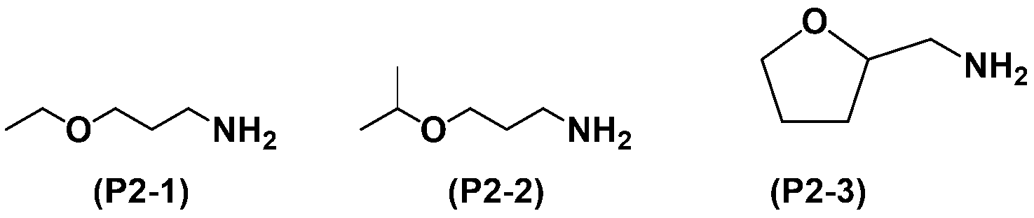
- amine compound represented by formula (P1) include, but are not limited to, the following compounds.
- the content of the amine compound represented by the formula (P1) is not particularly limited.
- the mass ratio is about 0.01 to 10 times, preferably about 0.01 to 8 times, more preferably about 0.01 to 6 times the mass of the charge-transporting substance 1. , and more preferably about 0.01 to 4 times the mass.
- the charge-transporting substance used in the present invention is not particularly limited, and may be appropriately selected from charge-transporting compounds, charge-transporting oligomers, charge-transporting polymers, etc. used in the field of organic EL devices and the like. can be done. Specific examples thereof include arylamine derivatives such as oligoaniline derivatives, N,N'-diarylbenzidine derivatives, N,N,N',N'-tetraarylbenzidine derivatives, oligothiophene derivatives, thienothiophene derivatives, and thienobenzothiophene.
- arylamine derivatives such as oligoaniline derivatives, N,N'-diarylbenzidine derivatives, N,N,N',N'-tetraarylbenzidine derivatives, oligothiophene derivatives, thienothiophene derivatives, and thienobenzothiophene.
- charge-transporting compounds such as thiophene derivatives such as derivatives, pyrrole derivatives such as oligopyrrole, charge-transporting oligomers, charge-transporting polymers such as polythiophene derivatives, polyaniline derivatives, and polypyrrole derivatives, etc., and polythiophene derivatives are particularly preferred.
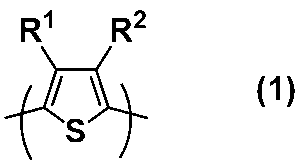
- the charge-transporting substance is a polythiophene derivative containing a repeating unit represented by formula (1) or an amine adduct thereof.
- R 1 and R 2 are each independently a hydrogen atom, an alkyl group having 1 to 40 carbon atoms, a fluoroalkyl group having 1 to 40 carbon atoms, an alkoxy group having 1 to 40 carbon atoms, or an alkoxy group having 1 to 40 carbon atoms.
- Y is an alkylene group having 1 to 40 carbon atoms which may contain an ether bond and may be substituted with a sulfonic acid group
- Z is substituted with a halogen atom is an alkylene group having 1 to 40 carbon atoms
- p is an integer of 1 or more
- R e is a hydrogen atom, an alkyl group having 1 to 40 carbon atoms, or a fluoroalkyl group having 1 to 40 carbon atoms.
- the alkyl group having 1 to 40 carbon atoms may be linear, branched, or cyclic, and specific examples thereof include the above-exemplified alkyl groups having 1 to 20 carbon atoms, behenyl group, and triacontyl group. and tetracontyl groups.
- an alkyl group having 1 to 18 carbon atoms is preferred, and an alkyl group having 1 to 8 carbon atoms is more preferred.
- the fluoroalkyl group having 1 to 40 carbon atoms is not particularly limited as long as it is an alkyl group having 1 to 40 carbon atoms in which at least one hydrogen atom on the carbon atoms is substituted with a fluorine atom.
- the alkyl group therein may be linear, branched or cyclic. Specific examples thereof include methoxy, ethoxy, n-propoxy, i- propoxy group, c-propoxy group, n-butoxy group, i-butoxy group, s-butoxy group, t-butoxy group, n-pentoxy group, n-hexoxy group, n-heptyloxy group, n-octyloxy group, n-nonyloxy group, n-decyloxy group, n-undecyloxy group, n-dodecyloxy group, n-tridecyloxy group, n-tetradecyloxy group, n-pentadecyloxy group, n-hexadecyloxy group , n-heptadecyloxy, n-octadecyloxy, n-non
- the fluoroalkoxy group having 1 to 40 carbon atoms is not particularly limited as long as it is an alkoxy group having 1 to 40 carbon atoms in which at least one hydrogen atom on the carbon atoms is substituted with a fluorine atom.
- fluoromethoxy group difluoromethoxy group, perfluoromethoxy group, 1-fluoroethoxy group, 2-fluoroethoxy group, 1,2-difluoroethoxy group, 1,1-difluoroethoxy group, 2,2-difluoroethoxy group, 1,1,2-trifluoroethoxy group, 1,2,2-trifluoroethoxy group, 2,2,2-trifluoroethoxy group, 1,1,2,2-tetrafluoroethoxy group, 1,2, 2,2-tetrafluoroethoxy group, perfluoroethoxy group, 1-fluoropropoxy group, 2-fluoropropoxy group, 3-fluoropropoxy group, 1,1-difluoropropoxy group, 1,2-difluoropropoxy group, 1, 3-difluoropropoxy group, 2,2-difluoropropoxy group, 2,3-difluoropropoxy group, 3,3-difluoropropoxy group, 1,1,2-
- the alkylene group having 1 to 40 carbon atoms may be straight-chain, branched-chain or cyclic, and specific examples thereof include the same as those exemplified above.
- aryl group having 6 to 20 carbon atoms examples are the same as those exemplified above. Phenyl, tolyl and naphthyl groups are preferred in the present invention.
- Examples of the aryloxy group having 6 to 20 carbon atoms include phenoxy group, anthracenoxy group, naphthoxy group, phenanthrenoxy group and fluorenoxy group.
- Halogen atoms include fluorine, chlorine, bromine and iodine atoms.
- R 1 and R 2 are each independently a hydrogen atom, a fluoroalkyl group having 1 to 40 carbon atoms, an alkoxy group having 1 to 40 carbon atoms, —O[C(R a R b )—C(R c R d )—O] p —R e , —OR f , or a sulfonic acid group, or —O—Y—O— formed by combining R 1 and R 2 is preferable.
- R a to R d each independently represent a hydrogen atom, an alkyl group having 1 to 40 carbon atoms, a fluoroalkyl group having 1 to 40 carbon atoms, or an aryl group having 6 to 20 carbon atoms; Specific examples are the same as those mentioned above. Among them, R a to R d are each independently preferably a hydrogen atom, an alkyl group having 1 to 8 carbon atoms, a fluoroalkyl group having 1 to 8 carbon atoms, or a phenyl group.
- R e is a hydrogen atom, an alkyl group having 1 to 8 carbon atoms, a fluoroalkyl group having 1 to 8 carbon atoms or a phenyl group, preferably a hydrogen atom, a methyl group, a propyl group or a butyl group. Also, p is preferably 1 to 5, more preferably 1, 2 or 3.
- R f is a hydrogen atom, an alkyl group having 1 to 40 carbon atoms, a fluoroalkyl group having 1 to 40 carbon atoms or an aryl group having 6 to 20 carbon atoms, but a hydrogen atom, an alkyl group having 1 to 8 carbon atoms, A fluoroalkyl group having 1 to 8 carbon atoms or a phenyl group is preferred, and -CH 2 CF 3 is more preferred.
- R 1 is preferably a hydrogen atom or a sulfonic acid group, more preferably a sulfonic acid group
- R 2 is preferably an alkoxy group having 1 to 40 carbon atoms or -O-[Z- O] p -R e , more preferably -O[C(R a R b )-C(R c R d )-O] p -R e or -OR f , even more preferably -O[C(R a R b )—C(R c R d )—O] p —R e , —O—CH 2 CH 2 —O—CH 2 CH 2 —O—CH 3 , —O—CH 2 CH 2 —O— CH 2 CH 2 --OH or --O--CH 2 CH 2 --OH or --O--Y--O-- formed by R 1 and R 2 joining together.
- the polythiophene derivative according to a preferred embodiment of the present invention contains a repeating unit in which R 1 is a sulfonic acid group and R 2 is other than a sulfonic acid group, or R 1 and R 2 are linked Including repeating units that are -O-Y-O- formed.
- the polythiophene derivative contains a repeating unit in which R 1 is a sulfonic acid group and R 2 is an alkoxy group having 1 to 40 carbon atoms or -O-[ZO] p -R e , or —O—Y—O— formed by combining R 1 and R 2 .
- R 1 is a sulfonic acid group and R 2 is —O[C(R a R b )–C(R c R d )–O] p —R e or — Contains repeat units that are OR f .
- R 1 is a sulfonic acid group and R 2 is —O[C(R a R b )–C(R c R d )–O] p —R e It includes a repeating unit or a repeating unit where R 1 and R 2 are joined to form -O-Y-O-.
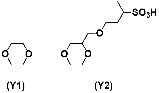
- R 1 is a sulfonic acid group and R 2 is --O--CH 2 CH 2 --O--CH 2 CH 2 --O--CH 3 or --O--CH 2 CH 2 —O—CH 2 CH 2 —OH or —O—CH 2 CH 2 —OH, or R 1 and R 2 are bonded to each other, and the following formulas (Y1) and (Y2) Includes repeat units that are represented groups.
- polythiophene derivatives include polythiophenes containing at least one repeating unit represented by the following formulas (1-1) to (1-5).
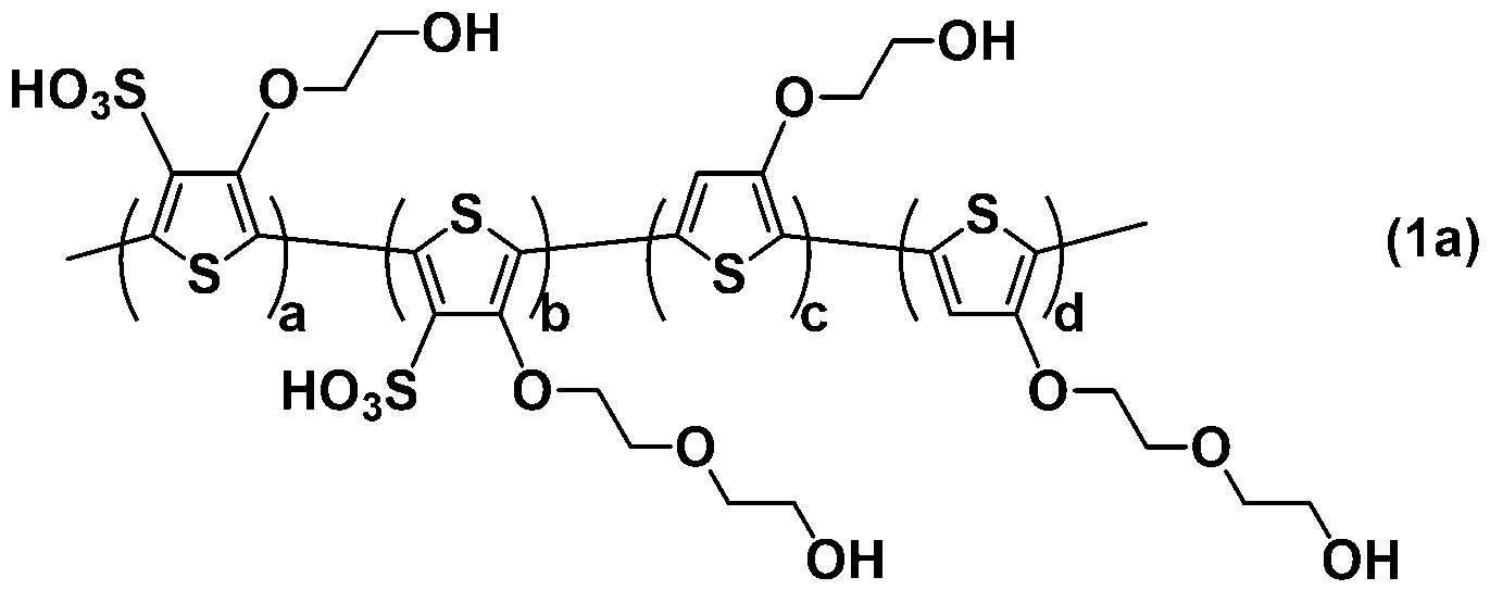
- examples of suitable structures of the above polythiophene derivatives include polythiophene derivatives having a structure represented by the following formula (1a).
- each unit may be combined randomly or may be combined as a block polymer.
- polythiophene derivatives may be homopolymers or copolymers (including statistical, random, gradient, and block copolymers).
- block copolymers include, for example, AB diblock copolymers, ABA triblock copolymers, and (AB) m -multiblock copolymers.
- Polythiophenes contain repeat units derived from other types of monomers such as thienothiophenes, selenophenes, pyrroles, furans, tellurophenes, anilines, arylamines, and arylenes such as phenylenes, phenylene vinylenes, and fluorenes. may contain.
- the content of the repeating unit represented by formula (1) in the polythiophene derivative is preferably more than 50 mol%, more preferably 80 mol% or more, more preferably 90 mol% of all repeating units contained in the polythiophene derivative.
- the above is more preferable, 95 mol % or more is more preferable, and 100 mol % is most preferable.
- the polymer formed may contain repeating units derived from impurities, depending on the purity of the starting monomers used for polymerization.
- the term "homopolymer” means a polymer containing repeating units derived from one type of monomer, but may contain repeating units derived from impurities.
- the polythiophene derivative is preferably a polymer in which basically all the repeating units are the repeating units represented by the above formula (1). ) is more preferably a polymer containing at least one repeating unit.
- the polythiophene derivative contains a repeating unit having a sulfonic acid group
- at least part of the sulfonic acid group contained in the polythiophene derivative is an amine compound. is preferably an amine adduct to which is added.
- Amine compounds that can be used to form amine adducts include methylamine, ethylamine, n-propylamine, isopropylamine, n-butylamine, isobutylamine, s-butylamine, t-butylamine, n-pentylamine, n-hexylamine.
- n-heptylamine, n-octylamine 2-ethylhexylamine, n-nonylamine, n-decylamine, n-undecylamine, n-dodecylamine, n-tridecylamine, n-tetradecylamine, n-penta Monoalkylamine compounds such as decylamine, n-hexadecylamine, n-heptadecylamine, n-octadecylamine, n-nonadecylamine, n-eicosanylamine; aniline, tolylamine, 1-naphthylamine, 2-naphthylamine, 1- anthrylamine, 2-anthrylamine, 9-anthrylamine, 1-phenanthrylamine, 2-phenanthrylamine, 3-phenanthrylamine, 4-phenanthrylamine, 9-phenanthrylamine Primary
- the above polythiophene derivative or its amine adduct may be treated with a reducing agent.
- some of the repeating units constituting them may have an oxidized chemical structure called a "quinoid structure".
- the term "quinoid structure” is used for the term “benzenoid structure”, the latter being a structure containing an aromatic ring, whereas the former is a structure in which the double bond within the aromatic ring moves out of the ring (the As a result, the aromatic ring disappears), meaning a structure in which two exocyclic double bonds conjugated with other double bonds remaining in the ring are formed.
- R 1 and R 2 are as defined in formula (1) above.
- This quinoid structure is generated by a process in which the polythiophene derivative containing the repeating unit represented by the above formula (1) undergoes an oxidation reaction by a dopant, a so-called doping reaction, and imparts charge transport properties to the polythiophene derivative. It forms part of a structure called "bipolaron structure". These structures are known. Introduction of a "polaron structure” and/or a “bipolaron structure” is essential in the production of an organic EL element, and in fact, when the thin film formed from the charge-transporting ink composition is baked when the organic EL element is produced. In addition, the above doping reaction is intentionally caused to achieve this.
- the reason why the quinoid structure is included in the polythiophene derivative before the doping reaction is that the polythiophene derivative undergoes an unintended oxidation reaction equivalent to the doping reaction during the manufacturing process (especially the sulfonation step therein). This is thought to be due to the
- the polythiophene derivative when the polythiophene derivative is subjected to a reduction treatment using a reducing agent, even if the quinoid structure is excessively introduced into the polythiophene derivative, the quinoid structure is reduced by the reduction, and the solubility and dispersibility of the polythiophene derivative in an organic solvent are improved. is improved, it becomes possible to stably produce a good charge-transporting ink composition that gives a thin film with excellent uniformity.
- the conditions for the reduction treatment are such that the quinoid structure is reduced to appropriately convert to the non-oxidized structure, that is, the benzenoid structure (for example, in the polythiophene derivative containing the repeating unit represented by the above formula (1),
- the quinoid structure represented by the above formula (1′) is not particularly limited as long as it can be converted to the structure represented by the above formula (1), for example, in the presence of a suitable solvent or
- This treatment can be carried out simply by contacting the polythiophene derivative or amine adduct with a reducing agent in the absence thereof.
- a reducing agent is not particularly limited as long as the reduction is performed properly, but suitable examples include aqueous ammonia, hydrazine, etc., which are readily available on the market.
- the amount of the reducing agent varies depending on the amount of the reducing agent to be used, and cannot be categorically defined. It is 0.1 parts by mass or more and 10 parts by mass or less from the viewpoint of preventing excess reducing
- a polythiophene derivative or an amine adduct is stirred overnight at room temperature in 28% ammonia water.
- the reduction treatment under such relatively mild conditions sufficiently improves the solubility and dispersibility of the polythiophene derivatives and amine adducts in organic solvents.
- the reduction treatment may be performed before forming the amine adduct or after forming the amine adduct.
- the solubility and dispersibility of the polythiophene derivative or its amine adduct in the solvent change, and as a result, the polythiophene derivative or its amine adduct, which was not dissolved in the reaction system at the start of the treatment, will be removed after the treatment is completed. Sometimes dissolved. In such a case, an organic solvent (acetone, isopropyl alcohol, etc. in the case of sulfonated polythiophene) incompatible with the polythiophene derivative or its amine adduct is added to the reaction system to obtain the polythiophene derivative or its amine adduct.
- the polythiophene derivative or its amine adduct can be recovered by a method such as causing precipitation and filtering.
- the weight average molecular weight of the polythiophene derivative containing the repeating unit represented by formula (1) or its amine adduct is preferably about 1,000 to 1,000,000, more preferably about 5,000 to 100,000, About 10,000 to about 50,000 is even more preferred.
- a weight average molecular weight is a polystyrene conversion value by a gel permeation chromatography.
- the polythiophene derivative or its amine adduct contained in the charge-transporting ink composition of the present invention may be only one polythiophene derivative or its amine adduct containing a repeating unit represented by formula (1). It may be more than seeds.
- a commercially available product or a product obtained by polymerizing a thiophene derivative or the like as a starting material by a known method may be used. It is also preferable to use those purified by methods such as reprecipitation and ion exchange. By using a purified product, the properties of the organic EL device provided with the thin film obtained from the charge-transporting ink composition of the present invention can be further enhanced.
- conjugated polymers and sulfonated conjugated polymers are described in US Pat. No. 8,017,241 to Seshadri et al. Sulfonated polythiophenes are also described in WO2008/073149 and WO2016/171935.
- At least part of the polythiophene derivative containing the repeating unit represented by formula (1) or its amine adduct contained in the charge-transporting ink composition is dissolved in an organic solvent.
- a polythiophene derivative containing a repeating unit represented by formula (1) or an amine adduct thereof and a charge-transporting substance other than the polythiophene derivative containing the repeating unit may be used in combination.
- the content of the charge-transporting substance in the charge-transporting ink composition of the present invention is usually 0.05 to 40% by mass, preferably 0.05 to 40% by mass, based on the solid content, taking into account the desired film thickness, the viscosity of the ink composition, and the like. is appropriately determined in the range of 0.1 to 35% by mass.
- the charge-transporting ink composition of the invention contains an organic solvent.
- an organic solvent is not particularly limited as long as it disperses or dissolves the solid content.
- aromatic or halogenated aromatic hydrocarbon solvents such as benzene, toluene, xylene, ethylbenzene and chlorobenzene; aliphatic hydrocarbons such as n-heptane, n-hexane and cyclohexane; diethyl ether, Ether solvents such as tetrahydrofuran, dioxane, and 1,2-dimethoxyethane; Ketone solvents such as acetone, methyl ethyl ketone, methyl isobutyl ketone, and cyclohexanone; Ethyl acetate, n-hexyl acetate, ethyl lactate, ⁇ -butyrolactone, propylene carbonate, malonic acid ester solvents such as diisoprop
- amide solvents 1,3-dimethyl-2-imidazolidinone, dipropylene glycol and dipropylene glycol monomethyl ether are more preferred.
- these organic solvents can be used individually or in mixture of 2 or more types, respectively.
- the charge-transporting ink composition of the present invention may contain water as a solvent, and the content of water is 10% by mass or less based on the total solvent from the viewpoint of obtaining an organic EL device having excellent durability with good reproducibility. It is preferable, more preferably 5% by mass or less, and it is optimal to use only an organic solvent as the solvent.
- “only organic solvent” means that only organic solvent is used as a solvent, and even the existence of "water” contained in a trace amount in the organic solvent or solid content used is denied. not something to do.
- the charge-transporting ink composition of the present invention may contain metal oxide nanoparticles.
- a nanoparticle means a fine particle having an average primary particle size of the order of nanometers (typically 500 nm or less).
- Metal oxide nanoparticles refer to metal oxides shaped into nanoparticles.
- the primary particle size of the metal oxide nanoparticles used in the present invention is not particularly limited as long as it is nano-sized, but considering obtaining a thin film with good reproducibility and excellent flatness, it is preferably 2 to 150 nm. , 3 to 100 nm, and even more preferably 5 to 50 nm.
- the particle size is a measured value using a nitrogen adsorption isotherm by the BET method.
- the metals constituting the metal oxide nanoparticles used in the present invention include not only metals in the usual sense, but also semimetals.
- Metals in the usual sense include, but are not limited to, tin (Sn), titanium (Ti), aluminum (Al), zirconium (Zr), zinc (Zn), niobium (Nb), tantalum ( It is preferable to use one or more selected from the group consisting of Ta) and tungsten (W).
- metalloids refer to elements whose chemical and/or physical properties are intermediate between those of metals and nonmetals. A universal definition of metalloids has not been established, but in the present invention, a total of six Let the elements be semimetals. These semimetals may be used alone or in combination of two or more, and may also be used in combination with metals in the usual sense.
- Metal oxide nanoparticles used in the present invention include boron (B), silicon (Si), germanium (Ge), arsenic (As), antimony (Sb), tellurium (Te), tin (Sn), titanium (Ti) , aluminum (Al), zirconium (Zr), zinc (Zn), niobium (Nb), tantalum (Ta) and tungsten (W).
- the metal oxide may be a mixture of oxides of individual single metals, or a composite oxide containing a plurality of metals.
- metal oxides include B2O3 , B2O , SiO2 , SiO, GeO2 , GeO , As2O4 , As2O3 , As2O5 , Sb2O3 , Sb2 . O5, TeO2, SnO2 , ZrO2 , Al2O3 , ZnO and the like, but also B2O3 , B2O , SiO2 , SiO , GeO2 , GeO , As2O4 , As2 . O3 , As2O5 , SnO2 , SnO, Sb2O3, TeO2 , and mixtures thereof are preferred, with SiO2 being more preferred.
- the metal oxide nanoparticles contained in the charge-transporting ink composition of the present invention may be of one type or two or more types.
- the metal oxide nanoparticles contained in the charge-transporting ink composition of the present invention are preferably uniformly dispersed in the composition.
- the metal oxide nanoparticles may contain one or more organic capping groups.
- This organic capping group may be reactive or non-reactive.
- Examples of reactive organic capping groups include organic capping groups that can be crosslinked by UV light or radical initiators.
- the content of the metal oxide nanoparticles is not particularly limited.
- the solid content of the charge-transporting ink composition is preferably 40 to 95% by mass, more preferably 50 to 95% by mass, and most preferably 60 to 90% by mass. .
- a composition in which metal oxide nanoparticles are uniformly dispersed can be prepared with good reproducibility. That is, rather than mixing and dispersing the metal oxide nanoparticles themselves in a solvent together with the charge-transporting substance or the like, a metal oxide nanoparticle sol is prepared in advance, and the charge-transporting substance or the like is dissolved or dissolved in the solvent. By mixing with the dispersed mixture, a charge-transporting ink composition in which the metal oxide nanoparticles are uniformly dispersed can be produced with good reproducibility.
- a metal oxide nanoparticle sol may be a commercially available product, or may be prepared by a known method using a solvent and metal oxide nanoparticles that may be contained in the charge-transporting ink composition of the present invention. .
- silica sol in which SiO 2 nanoparticles are dispersed in a dispersion medium.
- the silica sol is not particularly limited, and can be appropriately selected from known silica sols and used. Commercially available silica sols are usually in the form of dispersions.
- SiO2 nanoparticles are mixed with various solvents such as water, methanol, methyl ethyl ketone, methyl isobutyl ketone, N,N-dimethylacetamide, ethylene glycol, isopropanol, methanol, ethylene glycol monopropyl ether, cyclohexanone, acetic acid.
- solvents such as water, methanol, methyl ethyl ketone, methyl isobutyl ketone, N,N-dimethylacetamide, ethylene glycol, isopropanol, methanol, ethylene glycol monopropyl ether, cyclohexanone, acetic acid.
- solvents such as water, methanol, methyl ethyl ketone, methyl isobutyl ketone, N,N-dimethylacetamide, ethylene glycol, isopropanol, methanol, ethylene glycol monopropyl ether, cyclo
- a silica sol whose dispersion medium is an alcohol solvent, a glycol solvent or water is preferable, and a silica sol whose dispersion medium is an alcohol solvent or a glycol solvent is more preferable.
- a water-soluble alcohol or glycol-based solvent is preferable, and methanol, 2-propanol, and ethylene glycol are more preferable.
- silica sols include Snowtex (registered trademark) ST-O, ST-OS, ST-O-40 and ST-OL manufactured by Nissan Chemical Industries, Ltd., Silidodol 20 manufactured by Nippon Chemical Industries, Ltd., Water-dispersed silica sol such as 30, 40; Methanol silica sol, MA-ST-M, MA-ST-L, IPA-ST, IPA-ST-L, IPA-ST-ZL, EG-ST manufactured by Nissan Chemical Co., Ltd.
- organosilica sols such as
- the concentration of SiO 2 nanoparticles in silica sol is usually about 5 to 50% by mass.
- SiO 2 nanoparticles may aggregate, so this point should be taken into consideration when preparing the composition.
- the charge-transporting ink composition of the present invention contains an amine compound represented by formula (P1), a charge-transporting substance, and an organic solvent. may also contain dopant materials.
- the dopant substance is not particularly limited as long as it can be dispersed or dissolved in at least one solvent used in the charge-transporting ink composition, and both inorganic dopant substances and organic dopant substances can be used.
- the charge-transporting ink composition of the present invention contains a dopant substance, the content thereof is appropriately set in consideration of the type and amount of the charge-transporting substance. It ranges from 0.1 to 20.0 for the charge-transporting substance 1.
- Inorganic dopant substances include inorganic acids such as hydrogen chloride , sulfuric acid , nitric acid and phosphoric acid; ), boron trifluoride etherate (BF 3 OEt 2 ), iron chloride (III) (FeCl 3 ), copper chloride (II) (CuCl 2 ), antimony pentachloride (V) (SbCl 5 ), pentafluoride metal halides such as antimony (V) (SbF 5 ), arsenic pentafluoride (V) (AsF 5 ), phosphorus pentafluoride (PF 5 ), tris(4-bromophenyl)aluminum hexachloroantimonate (TBPAH); Halogens such as Cl 2 , Br 2 , I 2 , ICl, ICl 3 , IBr and IF 4 ; heteropolyacids such as phosphomolybdic acid and phosphotungstic acid;
- inorganic acids
- organic dopant substances include 7,7,8,8-tetracyanoquinodimethane (TCNQ), tetracyanoquinodimethane such as 2,5-difluoro-7,7,8,8-tetracyanoquinodimethane.
- TCNQ 7,7,8,8-tetracyanoquinodimethane
- tetracyanoquinodimethane such as 2,5-difluoro-7,7,8,8-tetracyanoquinodimethane.
- arylsulfonic acid compounds such as dinonylnaphthalenesulfonic acid derivatives described in JP-A-2005-108828 and aromatic sulfone compounds such as polystyrenesulfonic acid; and non-aromatic sulfone compounds such as 10-camphorsulfonic acid.
- aromatic sulfone compounds such as polystyrenesulfonic acid
- non-aromatic sulfone compounds such as 10-camphorsulfonic acid.
- arylsulfonic acid compounds are preferred in the present invention, and examples of preferred arylsulfonic acid compounds include arylsulfonic acid compounds represented by formula (H1) or (H2).
- a 1 represents O or S, with O being preferred.
- a 2 represents a naphthalene ring or an anthracene ring, preferably a naphthalene ring.
- a 3 represents a divalent to tetravalent perfluorobiphenyl group, s represents the number of bonds between A 1 and A 3 and is an integer satisfying 2 ⁇ s ⁇ 4, where A 3 is perfluorobiphenyldiyl is preferably a perfluorobiphenyl-4,4'-diyl group and s is 2.
- q represents the number of sulfonic acid groups bonded to A 2 and is an integer that satisfies 1 ⁇ q ⁇ 4, with 2 being optimal.
- a 4 to A 8 each independently represent a hydrogen atom, a halogen atom, a cyano group, an alkyl group having 1 to 20 carbon atoms, a halogenated alkyl group having 1 to 20 carbon atoms, or a halogenated group having 2 to 20 carbon atoms. It represents an alkenyl group, but at least three of A 4 to A 8 are halogen atoms.
- halogenated alkyl groups having 1 to 20 carbon atoms include trifluoromethyl group, 2,2,2-trifluoroethyl group, 1,1,2,2,2-pentafluoroethyl group, 3,3,3- trifluoropropyl group, 2,2,3,3,3-pentafluoropropyl group, 1,1,2,2,3,3,3-heptafluoropropyl group, 4,4,4-trifluorobutyl group, 3,3,4,4,4-pentafluorobutyl group, 2,2,3,3,4,4,4-heptafluorobutyl group, 1,1,2,2,3,3,4,4, A 4-nonafluorobutyl group and the like can be mentioned.
- halogenated alkenyl group having 2 to 20 carbon atoms examples include perfluorovinyl group, perfluoropropenyl group (allyl group), perfluorobutenyl group and the like.
- Other examples of the halogen atom and the alkyl group having 1 to 20 carbon atoms are the same as those mentioned above, but the halogen atom is preferably a fluorine atom.
- a 4 to A 8 are a hydrogen atom, a halogen atom, a cyano group, an alkyl group having 1 to 10 carbon atoms, a halogenated alkyl group having 1 to 10 carbon atoms, or a halogenated alkenyl group having 2 to 10 carbon atoms.
- a 4 to A 8 are preferably fluorine atoms, such as hydrogen atom, fluorine atom, cyano group, alkyl group having 1 to 5 carbon atoms, and It is more preferably a fluorinated alkyl group or a fluorinated alkenyl group having 2 to 5 carbon atoms, and at least three of A 4 to A 8 are fluorine atoms, a hydrogen atom, a fluorine atom, a cyano group, More preferably, it is a perfluoroalkyl group having 1 to 5 carbon atoms or a perfluoroalkenyl group having 1 to 5 carbon atoms, and A 4 , A 5 and A 8 are fluorine atoms.
- fluorine atoms such as hydrogen atom, fluorine atom, cyano group, alkyl group having 1 to 5 carbon atoms
- It is more preferably a fluorinated alkyl group or a fluorinated alkenyl group having 2 to 5
- the perfluoroalkyl group is a group in which all hydrogen atoms of an alkyl group are substituted with fluorine atoms
- the perfluoroalkenyl group is a group in which all hydrogen atoms of an alkenyl group are substituted with fluorine atoms.
- r represents the number of sulfonic acid groups bonded to the naphthalene ring and is an integer that satisfies 1 ⁇ r ⁇ 4, preferably 2 to 4, and most preferably 2.
- the molecular weight of an organic compound is preferably 3,000 or less, more preferably 2,500 or less, considering its solubility in organic solvents.
- the molecular weight of the arylsulfonic acid compound used as the dopant substance is not particularly limited, but is preferably 2,000 or less, more preferably 1,500 or less, in consideration of solubility in organic solvents.
- amine compound represented by formula (P1) for the purpose of improving the dispersibility and solubility of a charge-transporting substance such as a polythiophene derivative or an amine adduct thereof, together with an amine compound represented by formula (P1), Other amine compounds may also be included.
- Such other amine compound is not particularly limited as long as it dissolves in at least one solvent used in the ink composition, and may be one kind alone or two or more kinds.
- primary amine compounds include methylamine, ethylamine, n-propylamine, isopropylamine, n-butylamine, isobutylamine, s-butylamine, t-butylamine, n-pentylamine, n-hexylamine and n-heptyl.
- n-octylamine 2-ethylhexylamine, n-nonylamine, n-decylamine, n-undecylamine, n-dodecylamine, n-tridecylamine, n-tetradecylamine, n-pentadecylamine, n -monoalkylamine compounds such as hexadecylamine, n-heptadecylamine, n-octadecylamine, n-nonadecylamine, n-eicosanylamine; aniline, tolylamine, 1-naphthylamine, 2-naphthylamine, 1-anthrylamine, Monoaryls such as 2-anthrylamine, 9-anthrylamine, 1-phenanthrylamine, 2-phenanthrylamine, 3-phenanthrylamine, 4-phenanthrylamine and 9-phenanthrylamine
- secondary amine compounds include N-ethylmethylamine, N-methyl-n-propylamine, N-methylisopropylamine, N-methyl-n-butylamine, N-methyl-s-butylamine, N-methyl -t-butylamine, N-methylisobutylamine, diethylamine, N-ethyl-n-propylamine, N-ethylisopropylamine, N-ethyl-n-butylamine, N-ethyl-s-butylamine, N-ethyl-t- Butylamine, dipropylamine, Nn-propylisopropylamine, Nn-propyl-n-butylamine, Nn-propyl-s-butylamine, diisopropylamine, Nn-butylisopropylamine, Nt-butyl Isopropylamine, di(n-butyl)amine, di(s-butyl)
- tertiary amine compounds include N,N-dimethylethylamine, N,N-dimethyl-n-propylamine, N,N-dimethylisopropylamine, N,N-dimethyl-n-butylamine, N,N- Dimethyl-s-butylamine, N,N-dimethyl-t-butylamine, N,N-dimethylisobutylamine, N,N-diethylmethylamine, N-methyldi(n-propyl)amine, N-methyldiisopropylamine, N- methyldi(n-butyl)amine, N-methyldiisobutylamine, triethylamine, N,N-diethyl-n-butylamine, N,N-diisopropylethylamine, N,N-di(n-butyl)ethylamine, tri(n-propyl) ) trialkylamine compounds such as amine, tri
- the charge-transporting ink composition of the present invention contains other amine compounds, it should be excellent in the ability to improve the dispersibility and solubility of the charge-transporting substance such as the polythiophene derivative or its amine adduct used in the present invention. Therefore, the other amine compound preferably contains a primary amine compound, preferably a monoalkylamine, particularly a monoalkylamine having 2 to 20 carbon atoms.
- the content thereof is usually about 10 times the mass of the charge-transporting substance such as the polythiophene derivative or its amine adduct used in the present invention. It is below.
- Heteropolyacids can also be suitably used as dopant substances.
- Heteropolyacid has a structure in which a heteroatom is located at the center of the molecule, typically represented by a Keggin-type chemical structure represented by formula (A) or a Dawson-type chemical structure represented by formula (B), and vanadium ( V), molybdenum (Mo), tungsten (W), and other oxyacid isopolyacids are polyacids formed by condensation with oxyacids of different elements.
- Oxygen acids of such dissimilar elements mainly include oxyacids of silicon (Si), phosphorus (P), and arsenic (As).
- heteropolyacid examples include phosphomolybdic acid, silicomolybdic acid, phosphotungstic acid, silicotungstic acid, phosphotungstomolybdic acid, etc. These may be used alone or in combination of two or more. good.
- the heteropolyacid used in the present invention is available as a commercial product, and can also be synthesized by a known method.
- the one type of heteropolyacid preferably includes tungsten. That is, phosphotungstic acid, silicotungstic acid, phosphotungstomolybdic acid and the like are preferred, and phosphotungstic acid and silicotungstic acid are more preferred.
- the heteropolyacid may be obtained as a commercial product, or may be obtained as an appropriate product according to a known synthesis method, even if the number of elements is large or small from the structure represented by the general formula.
- phosphotungstic acid is generally represented by the chemical formula H 3 (PW 12 O 40 ) ⁇ nH 2 O, but in quantitative analysis, P (phosphorus), O (oxygen) or W Even if the number of (tungsten) is large or small, it can be used in the present invention as long as it is commercially available or synthesized appropriately according to a known synthesis method.
- the mass of the heteropolyacid defined in the present invention is not the mass of pure phosphotungstic acid (phosphotungstic acid content) in synthetic products or commercial products, but the commercially available form and known synthesis In a form that can be isolated by the method, it means the total mass in a state containing water of hydration and other impurities.
- the charge-transporting ink composition of the invention may contain a known organic silane compound.
- a known organic silane compound By including such an organic silane compound in the charge-transporting ink composition, when the charge-transporting thin film obtained from the ink composition is used as a hole injection layer of an organic EL device, holes are provided so as to be in contact with the hole injection layer. The hole injection property to the transport layer can be improved.
- alkoxysilane is preferable, and trialkoxysilane and tetraalkoxysilane are more preferable.
- alkoxysilanes include tetraethoxysilane, tetramethoxysilane, tetraisopropoxysilane, phenyltriethoxysilane, phenyltrimethoxysilane, methyltriethoxysilane, methyltrimethoxysilane, and 3,3,3-trifluoropropyltrimethoxysilane.
- Examples include silane, dimethyldiethoxysilane, dimethyldimethoxysilane, and the like.
- tetraethoxysilane TEOS
- tetramethoxysilane tetramethoxysilane
- tetraisopropoxysilane can be preferably used in the present invention.
- organic silane compounds can be used singly or in combination of two or more.
- the charge-transporting ink composition of the present invention contains an organic silane compound
- the content thereof is usually about 0.1 to 50% by mass based on the solid content. Considering the balance of suppressing deterioration of transportability, etc., it is preferably about 0.5 to 40% by mass, more preferably about 0.8 to 30% by mass, and even more preferably about 1 to 20% by mass.
- the viscosity of the charge-transporting ink composition of the invention is usually 1 to 50 mPa ⁇ s at 25°C, and the surface tension is usually 20 to 50 mN/m at 25°C.
- the viscosity and surface tension of the charge-transporting ink composition of the present invention are determined by changing the type of organic solvent used, their ratio, the solid content concentration, etc., in consideration of various factors such as the coating method used and the desired film thickness. can be adjusted by
- the solid content concentration of the charge-transporting ink composition of the present invention is appropriately set in consideration of the viscosity and surface tension of the charge-transporting ink composition, the thickness of the thin film to be produced, and the like. It is usually about 0.1 to 15% by mass, preferably 10% by mass or less, more preferably 8% by mass, from the viewpoint of suppressing aggregation of the charge-transporting substance and metal oxide nanoparticles in the ink composition. Below, it is more preferably 6% by mass or less.
- the amine compound represented by formula (P1), the charge-transporting substance and the solvent, and optionally the , metal oxide nanoparticles and dopant materials can be mixed in any order. That is, for example, a method of dissolving a charge-transporting substance and an amine compound represented by formula (P1) in a solvent to obtain a solution, and then dissolving a dopant substance in the solution; , a method of dissolving the charge-transporting substance and the amine compound represented by formula (P1) in the solution, mixing the amine compound represented by formula (P1), the charge-transporting substance, and the dopant substance, Any method of dissolving the mixture by adding it to a solvent can be employed as long as the solid content is uniformly dissolved or dispersed in the solvent.
- a method of adding an aqueous dispersion or an organic solvent dispersion of the metal oxide nanoparticles at any time in the above method, or a method of adding an aqueous dispersion or an organic solvent of the metal oxide nanoparticles A method of adding a previously prepared solution containing the amine compound represented by the formula (P1) and the charge-transporting substance and other components or a solution thereof to the dispersion is included. It should be noted that the charge-transporting substance and metal oxide nanoparticles may aggregate or precipitate when mixed, depending on the type and amount of the solvent used together. In the preparation of the charge-transporting ink composition, the composition may be appropriately heated as long as the components are not decomposed or altered.
- the charge-transporting ink composition is prepared in a submicron state during the production of the charge-transporting ink composition or after all components are mixed, for the purpose of obtaining a highly flat thin film with good reproducibility. It may be filtered using a meter-order filter or the like.
- a charge-transporting thin film can be formed on the substrate by applying the charge-transporting ink composition described above onto the substrate and baking it.
- the method for applying the ink composition is not particularly limited, and includes dipping, spin coating, transfer printing, roll coating, brush coating, inkjet, spraying, slit coating, and the like. It is preferable to adjust the viscosity and surface tension of the ink composition according to the method.
- the firing atmosphere is not particularly limited.
- a thin film having properties can be obtained.
- the firing temperature is appropriately set within a range of about 100 to 260° C. in consideration of the use of the obtained thin film, the degree of charge transport property to be imparted to the obtained thin film, the type and boiling point of the solvent, etc.
- the temperature is preferably about 140 to 250°C, more preferably about 145 to 240°C. It should be noted that, during the firing, the temperature may be changed in two or more stages for the purpose of expressing a higher uniform film-forming property or promoting the reaction on the substrate. Suitable equipment such as an oven may be used.
- the thickness of the charge-transporting thin film is not particularly limited, but when it is used as a functional layer provided between the anode and the light-emitting layer, such as a hole injection layer, a hole transport layer, and a hole injection transport layer of an organic EL device. , 5 to 300 nm.
- a method for changing the film thickness there are methods such as changing the solid content concentration in the charge-transporting ink composition and changing the amount of the solution on the substrate during coating.
- the organic EL device of the present invention has a pair of electrodes, and between these electrodes a charge transport layer comprising the charge transport thin film of the present invention.
- Typical structures of the organic EL element include (a) to (f) below, but are not limited to these.
- an electron blocking layer or the like may be provided between the light emitting layer and the anode, and a hole blocking layer or the like may be provided between the light emitting layer and the cathode, if necessary.
- the hole injection layer, the hole transport layer or the hole injection transport layer may also function as an electron blocking layer or the like, and the electron injection layer, the electron transport layer or the electron injection transport layer may contain holes (holes). It may also have a function as a block layer or the like.
- anode/hole-injection layer/hole-transport layer/light-emitting layer/electron-transport layer/electron-injection layer/cathode (b) anode/hole-injection layer/hole-transport layer/light-emitting layer/electron-injection-transport layer/ Cathode (c) anode/hole injection transport layer/light emitting layer/electron transport layer/electron injection layer/cathode (d) anode/hole injection transport layer/light emitting layer/electron injection transport layer/cathode (e) anode/positive Hole-injection layer/hole-transport layer/light-emitting layer/cathode (f) Anode/hole-injection-transport layer/light-emitting layer/cathode
- Hole injection layer is layers formed between a light-emitting layer and an anode that transport holes from the anode to the light-emitting layer.
- a hole-transporting material is provided between the light-emitting layer and the anode, it is a "hole-injection-transport layer", and between the light-emitting layer and the anode,
- the layer close to the anode is the “hole-injecting layer” and the other layer is the “hole-transporting layer”.
- the hole-injecting (transporting) layer is a thin film that is excellent not only in the ability to accept holes from the anode but also in the ability to inject holes into the hole-transporting (light-emitting) layer.
- Electrode injection layer is layers formed between a light-emitting layer and a cathode, and have the function of transporting electrons from the cathode to the light-emitting layer.
- a “light-emitting layer” is an organic layer having a light-emitting function, and includes a host material and a dopant material when a doping system is employed.
- the host material mainly promotes recombination of electrons and holes and has the function of confining excitons in the light-emitting layer, and the dopant material efficiently emits the excitons obtained by recombination. have a function.
- the host material mainly functions to confine excitons generated by the dopant within the light-emitting layer.
- a charge-transporting thin film prepared from the charge-transporting ink composition of the present invention can be used as a functional layer formed between an anode and a light-emitting layer in an organic EL device. It is suitable as a layer and a hole injection transport layer, more suitable as a hole injection layer and a hole transport layer, and even more suitable as a hole injection layer.
- Examples of the materials to be used and the manufacturing method for manufacturing an EL element using the charge-transporting ink composition of the present invention include, but are not limited to, the following.
- An example of a method for producing an OLED device having a hole injection layer made of a thin film obtained from the charge-transporting ink composition of the present invention is as follows.
- the electrodes are preferably cleaned with alcohol, pure water, or the like, or surface-treated with UV ozone treatment, oxygen-plasma treatment, or the like in advance, as long as the electrodes are not adversely affected.
- a hole injection layer is formed on the anode substrate using the charge-transporting ink composition by the method described above. This is introduced into a vacuum vapor deposition apparatus, and a hole transport layer, a light-emitting layer, an electron transport layer/hole blocking layer, an electron injection layer, and a cathode metal are sequentially vapor-deposited.
- a composition for forming a hole-transporting layer containing a hole-transporting polymer and a composition for forming a light-emitting layer containing a light-emitting polymer are used. are used to form these layers by a wet process.
- An electron blocking layer may be provided between the light-emitting layer and the hole-transporting layer, if necessary.
- Anode materials include transparent electrodes typified by indium tin oxide (ITO) and indium zinc oxide (IZO), and metal anodes composed of metals typified by aluminum, alloys thereof, etc. Those subjected to planarization treatment are preferable. Polythiophene derivatives and polyaniline derivatives having high charge transport properties can also be used. Other metals constituting the metal anode include gold, silver, copper, indium, and alloys thereof, but are not limited to these.
- Materials for forming the hole transport layer include (triphenylamine) dimer derivatives, [(triphenylamine) dimer] spirodimer, N,N'-bis(naphthalene-1-yl)-N,N'-bis (Phenyl)-benzidine ( ⁇ -NPD), 4,4′,4′′-tris[3-methylphenyl(phenyl)amino]triphenylamine (m-MTDATA), 4,4′,4′′-tris[1 -triarylamines such as naphthyl(phenyl)amino]triphenylamine (1-TNATA), 5,5′′-bis- ⁇ 4-[bis(4-methylphenyl)amino]phenyl ⁇ -2,2′: oligothiophenes such as 5′,2′′-terthiophene (BMA-3T);
- Materials for forming the light-emitting layer include metal complexes such as aluminum complexes of 8-hydroxyquinoline, metal complexes of 10-hydroxybenzo[h]quinoline, bisstyrylbenzene derivatives, bisstyrylarylene derivatives, (2-hydroxyphenyl)benzo Low-molecular light-emitting materials such as thiazole metal complexes and silol derivatives; poly(p-phenylenevinylene), poly[2-methoxy-5-(2-ethylhexyloxy)-1,4-phenylenevinylene], poly(3-alkyl thiophene), polyvinyl carbazole, etc., mixed with a light-emitting material and an electron transfer material, but not limited to these.
- metal complexes such as aluminum complexes of 8-hydroxyquinoline, metal complexes of 10-hydroxybenzo[h]quinoline, bisstyrylbenzene derivatives, bisstyrylarylene derivatives, (2-hydroxyphenyl)benz
- the light-emitting layer when it is formed by vapor deposition, it may be co-deposited with a light - emitting dopant.
- a light - emitting dopant such as rubrene, quinacridone derivatives, condensed polycyclic aromatic rings such as perylene, and the like, but are not limited thereto.
- Materials for forming the electron-transporting layer/hole-blocking layer include, but are not limited to, oxydiazole derivatives, triazole derivatives, phenanthroline derivatives, phenylquinoxaline derivatives, benzimidazole derivatives, pyrimidine derivatives, and the like.
- Materials for forming the electron injection layer include metal oxides such as lithium oxide (Li 2 O), magnesium oxide (MgO), alumina (Al 2 O 3 ), lithium fluoride (LiF), and sodium fluoride (NaF). and the like, but are not limited to these.
- Cathode materials include, but are not limited to, aluminum, magnesium-silver alloys, aluminum-lithium alloys, and the like.
- Materials for forming the electron blocking layer include, but are not limited to, tris(phenylpyrazole) iridium.
- hole-transporting polymers include poly[(9,9-dihexylfluorenyl-2,7-diyl)-co-(N,N'-bis ⁇ p-butylphenyl ⁇ -1,4-diaminophenylene )], poly[(9,9-dioctylfluorenyl-2,7-diyl)-co-(N,N′-bis ⁇ p-butylphenyl ⁇ -1,1′-biphenylene-4,4-diamine )], poly[(9,9-bis ⁇ 1′-penten-5′-yl ⁇ fluorenyl-2,7-diyl)-co-(N,N′-bis ⁇ p-butylphenyl ⁇ -1,4 -diaminophenylene)], poly[N,N'-bis(4-butylphenyl)-N,N'-bis(phenyl)-benzidine]-endcapped with polysilsiquinoxane,
- light-emitting polymers examples include polyfluorene derivatives such as poly(9,9-dialkylfluorene) (PDAF), poly(2-methoxy-5-(2′-ethylhexoxy)-1,4-phenylene vinylene) (MEH- PPV) and other polyphenylene vinylene derivatives, poly(3-alkylthiophene) (PAT) and other polythiophene derivatives, and polyvinylcarbazole (PVCz).
- PDAF poly(9,9-dialkylfluorene)
- MEH- PPV poly(2-methoxy-5-(2′-ethylhexoxy)-1,4-phenylene vinylene)
- PAT poly(3-alkylthiophene)
- PVCz polyvinylcarbazole
- the materials for the anode, cathode, and layers formed between them differ depending on whether the device has a bottom emission structure or a top emission structure.
- a transparent anode is used on the substrate side, and light is extracted from the substrate side
- a reflective anode made of metal is used, and light is emitted in the opposite direction to the substrate. Since light is extracted from a certain transparent electrode (cathode) side, for example, regarding the anode material, a transparent anode such as ITO is used when manufacturing an element with a bottom emission structure, and Al is used when manufacturing an element with a top emission structure.
- a reflective anode such as /Nd is used, respectively.
- the organic EL element of the present invention may be sealed together with a water capturing agent or the like according to a standard method in order to prevent property deterioration.
- the charge-transporting ink composition of the present invention is suitably used for forming the functional layer formed between the anode and the light-emitting layer of the organic EL element as described above, but it can also be used for organic photoelectric conversion elements and organic thin films.
- a method for improving the storage stability of a charge-transporting ink composition of the present invention is a method for improving the storage stability of a charge-transporting ink composition containing an amine compound, a charge-transporting substance, and an organic solvent,
- the amine compound an amine compound represented by the above formula (P1) is used, and suitable conditions such as the type and amount of the solid content of the amine compound, the charge-transporting substance, etc. and the organic solvent are the same as above. be.
- the improvement in the storage stability of the charge-transporting ink composition can be evaluated by the change in absorbance.
- the absorbance of the charge-transporting ink composition before exposure to the atmosphere is a (initial)
- the absorbance of the charge-transporting ink composition after exposure for 10 days is a (exposure to the atmosphere) at the maximum absorption (for example, wavelength of 620 nm).
- the rate of change in absorbance (%) ⁇ a/a (initial) as an absolute value, usually 10 % or less, preferably 9% or less, more preferably 8% or less, still more preferably 7% or less, and even more preferably 6% or less.
- the method for improving the flatness of a charge-transporting thin film of the present invention is a method for improving the flatness of a charge-transporting thin film obtained from a charge-transporting ink composition containing an amine compound, a charge-transporting substance, and an organic solvent.
- the solid content of the amine compound, the charge-transporting substance, etc. and the preferred conditions such as the type and amount of the organic solvent and the conditions for forming the charge-transporting thin film are the same as above.
- the improvement in the flatness of the charge-transporting thin film can be evaluated by the average surface roughness Ra.
- the average surface roughness Ra (nm) is usually 2.80 nm or less, It is preferably 2.70 nm or less, more preferably 2.60 nm or less, and preferably 2.50 nm or less.
- the average surface roughness (Ra) of the charge-transporting thin film is determined by, for example, an atomic force microscope Park-NX10 manufactured by Park Systems and a cantilever for measuring average surface roughness OMCL-AC 160TS 10M manufactured by Olympus. can be measured using
- Preparation Example 2 100 g of ST-OS (manufactured by Nissan Chemical Co., Ltd.), which is a water-dispersed silica sol, and dipropylene glycol monomethyl ether (manufactured by Kanto Chemical Co., Ltd., hereinafter the same) are placed in an eggplant flask, and the ST-OS is evaporated using an evaporator. Water contained in was replaced with dipropylene glycol monomethyl ether to obtain a silica sol (silica concentration: 9.43% by mass) using dipropylene glycol monomethyl ether as a dispersion medium.
- ST-OS manufactured by Nissan Chemical Co., Ltd.
- dipropylene glycol monomethyl ether manufactured by Kanto Chemical Co., Ltd., hereinafter the same
- Example 1-2 3.24 g of 1,3-dimethyl-2-imidazolidinone, 5.17 g of dipropylene glycol and 3.55 g of dipropylene glycol monomethyl ether were placed in an Erlenmeyer flask and stirred at room temperature for 30 minutes using a stirrer. After that, 0.21 g of the 1,3-dimethyl-2-imidazolidinone solution of the arylsulfonic acid compound A obtained in Preparation Example 1 was added and stirred at room temperature for 30 minutes using a stirrer.
- Example 2-1 Preparation of charge-transporting thin film and evaluation of average surface roughness Ra
- the charge-transporting ink composition obtained in Example 1-1 was applied to an ITO substrate using a spin coater, heated at 120° C. for 1 minute in the air, and then heated at 230° C. for 15 minutes. A uniform thin film with a thickness of 30 nm was formed thereon.
- As the ITO substrate a 25 mm ⁇ 25 mm ⁇ 0.7 t glass substrate on which indium tin oxide (ITO) was patterned to a thickness of 50 nm was used. , for 30 seconds) to remove impurities on the surface.
- ITO indium tin oxide
- Example 2-2 Comparative Examples 2-1 to 2-2
- Example 1-1 the charge-transporting ink compositions obtained in Example 1-2 and Comparative Examples 1-1 and 1-2 were used.
- a uniform thin film with a thickness of 30 nm was formed on an ITO substrate in the same manner as in 2-1.
- Example 2-1 For the charge-transporting thin films on the ITO substrates formed in Example 2-1, Example 2-2, Comparative Examples 2-1 and 2-2, the average surface roughness Ra was evaluated using an atomic force microscope. did. The measurement range of the atomic force microscope was 3 ⁇ m ⁇ 3 ⁇ m. Table 1 shows the results.
- the average surface roughness of the thin film formed from the charge-transporting ink composition of the present invention was lower than that of the thin film formed from the charge-transporting ink composition of the comparative example.
- the use of the amine compound represented by the formula (P1) contained in the charge-transporting ink composition of the present invention makes it possible to realize a more stable interaction between the amine compound and the charge-transporting substance, resulting in It is presumed that this is because aggregation of the charge-transporting substance was alleviated or suppressed in the heating process after the application of the substance.
- Example 3-1 Evaluation of stability of charge-transporting ink composition against atmospheric exposure
- 0.2 g of the charge-transporting ink composition obtained in Example 1-1 was mixed with 4.14 g of 1,3-dimethyl-2-imidazolidinone, 4.83 g of dipropylene glycol and 4.83 g of dipropylene glycol monomethyl ether. and the absorption spectrum of the resulting mixture was measured.
- 3.0 g of the charge-transporting ink composition obtained in Example 1-1 was added to a 20-mL glass vial, and the vial was left open for 10 days at room temperature in the atmosphere. exposed to air.
- Example 3-2 Comparative Examples 3-1 to 3-2
- the charge-transporting ink compositions obtained in Example 1-2 and Comparative Examples 1-1 and 1-2 were used instead of the charge-transporting ink composition obtained in Example 1-1.
- the absorption spectrum was measured in the same manner as in Example 3-1.
- Fig. 1 shows the measured absorption spectrum.
- the absorbance of the charge-transporting ink composition before exposure to the atmosphere (a (initial)
- the absorbance of the charge-transporting ink composition after exposure for 10 days (a (exposure to atmosphere)
- Table 2 shows the difference in absorbance ( ⁇ a) before and after exposure to the atmosphere and the rate of change in absorbance (%).
- the change in absorbance of the charge-transporting ink composition of the present invention was smaller than that of the charge-transporting ink composition of the comparative example. This is because by using the amine compound represented by formula (P1) contained in the charge-transporting ink composition of the present invention, a stable interaction between the amine compound and the charge-transporting substance in the composition can be realized. It is presumed that this is because the oxidation of the charge-transporting substance is suppressed.
- Example 4-1 Fabrication and property evaluation of organic EL device
- the charge-transporting ink composition obtained in Example 1-1 was applied to an ITO substrate using a spin coater, heated at 120° C. for 1 minute in the air, and then heated at 230° C. for 15 minutes. A uniform charge-transporting thin film having a thickness of 30 nm was formed thereon.
- As the ITO substrate a 25 mm ⁇ 25 mm ⁇ 0.7 t glass substrate having a patterned ITO film with a thickness of 150 nm formed on the surface was used. to remove impurities on the surface.
- ⁇ -NPD N,N'-di(1-naphthyl)-N
- a vapor deposition apparatus degree of vacuum: 1.0 ⁇ 10 -5 Pa
- N′-diphenylbenzidine was deposited at a rate of 0.2 nm/second to a thickness of 30 nm.
- an electron block material HTEB-01 manufactured by Kanto Kagaku Co., Ltd.
- the vapor deposition rate was 0.2 nm/sec for Alq 3 and aluminum, and 0.02 nm/sec for lithium fluoride, respectively, and the film thicknesses were 20 nm, 0.5 nm and 80 nm, respectively.
- the characteristics of the organic EL element were evaluated after being sealed with a sealing substrate. Sealing was performed by the following procedure. In a nitrogen atmosphere with an oxygen concentration of 2 ppm or less and a dew point of ⁇ 76° C. or less, the organic EL element was placed between the sealing substrates, and the sealing substrates were coated with an adhesive (manufactured by MORESCO Co., Ltd., MORESCO Moisture Cut WB90US (P)). pasted together by At this time, a water capturing agent (HD-071010W-40 manufactured by Dainic Co., Ltd.) was placed in the sealing substrate together with the organic EL element. The bonded sealing substrates were irradiated with UV light (wavelength: 365 nm, irradiation amount: 6,000 mJ/cm 2 ) and then annealed at 80° C. for 1 hour to cure the adhesive.
- an adhesive manufactured by MORESCO Co., Ltd., MORESCO Moisture Cut WB90US (P)
- Example 4-2 In the same manner as in Example 4-1, except that the charge-transporting ink composition obtained in Example 1-2 was used instead of the charge-transporting ink composition obtained in Example 1-1. An organic EL device was obtained.
Landscapes
- Chemical & Material Sciences (AREA)
- Engineering & Computer Science (AREA)
- Organic Chemistry (AREA)
- Life Sciences & Earth Sciences (AREA)
- Materials Engineering (AREA)
- Wood Science & Technology (AREA)
- Optics & Photonics (AREA)
- Physics & Mathematics (AREA)
- Chemical Kinetics & Catalysis (AREA)
- Medicinal Chemistry (AREA)
- Polymers & Plastics (AREA)
- Manufacturing & Machinery (AREA)
- Health & Medical Sciences (AREA)
- Electroluminescent Light Sources (AREA)
- Organic Low-Molecular-Weight Compounds And Preparation Thereof (AREA)
- Inks, Pencil-Leads, Or Crayons (AREA)
Abstract
Description
1. 下記式(P1)で表されるアミン化合物と、電荷輸送性物質と、有機溶媒とを含むことを特徴とする電荷輸送性インク組成物。

2. 上記Rmが、炭素数1~20のアルキル基であり、上記Rnが、炭素数1~20のアルキレン基である1の電荷輸送性インク組成物。
3. 上記電荷輸送性物質が、下記式(1)で表される繰り返し単位を含むポリチオフェン誘導体またはそのアミン付加体である1または2の電荷輸送性インク組成物。
4. 上記R1が、スルホン酸基であり、上記R2が、炭素数1~40のアルコキシ基もしくは-O-[Z-O]p-Reである、または上記R1およびR2が結合して形成される-O-Y-O-である3の電荷輸送性インク組成物。
5. さらに、ドーパント物質を含む1~4のいずれかの電荷輸送性インク組成物。
6. 上記ドーパント物質が、アリールスルホン酸化合物およびヘテロポリ酸化合物よりなる群から選ばれる少なくとも1種を含む5の電荷輸送性インク組成物。
7. さらに、金属酸化物ナノ粒子を含む1~6のいずれかの電荷輸送性インク組成物。
8. 1~7のいずれかの電荷輸送性インク組成物から得られる電荷輸送性薄膜。
9. 8の電荷輸送性薄膜を有する電子素子。
10. 有機エレクトロルミネッセンス素子である9の電子素子。
11. アミン化合物と、電荷輸送性物質と、有機溶媒とを含む電荷輸送性インク組成物の保存安定性の向上方法であって、上記アミン化合物として、下記式(P1)で表されるアミン化合物を用いることを特徴とする電荷輸送性インク組成物の保存安定性の向上方法。

12. アミン化合物と、電荷輸送性物質と、有機溶媒とを含む電荷輸送性インク組成物から得られる電荷輸送性薄膜の平坦性の向上方法であって、
上記アミン化合物として、下記式(P1)で表されるアミン化合物を用いることを特徴とする電電荷輸送性薄膜の平坦性の向上方法。

本発明の電荷輸送性インク組成物は、下記式(P1)で表されるアミン化合物と、電荷輸送性物質と、有機溶媒とを含むものである。なお、本発明においては、本発明の電荷輸送性インク組成物に関する「固形分」とは、当該組成物に含まれる溶媒以外の成分を意味する。また、電荷輸送性とは、導電性と同義であり、正孔輸送性とも同義である。本発明の電荷輸送性インク組成物は、それ自体に電荷輸送性があるものでもよく、組成物を使用して得られる固体膜に電荷輸送性があるものでもよい。

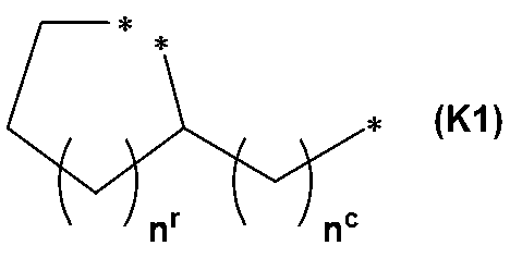
上記nrとncの組み合わせとしては、好ましくはnrとncはともに1~3であり、より好ましくnrとncはともに1~2であり、より一層好ましくnrは1~2であり、ncは1であり、更に好ましくはnrとncはともに1である。
その具体例としては、オリゴアニリン誘導体、N,N'-ジアリールベンジジン誘導体、N,N,N',N'-テトラアリールベンジジン誘導体等のアリールアミン誘導体、オリゴチオフェン誘導体、チエノチオフェン誘導体、チエノベンゾチオフェン誘導体等のチオフェン誘導体、オリゴピロール等のピロール誘導体などの各種電荷輸送性化合物や電荷輸送性オリゴマー、ポリチオフェン誘導体、ポリアニリン誘導体、ポリピロール誘導体等の電荷輸送性ポリマー等が挙げられ、特にポリチオフェン誘導体が好ましい。
好ましい一態様においては、上記電荷輸送性物質は、式(1)で表される繰り返し単位を含むポリチオフェン誘導体またはそのアミン付加体である。

Ra~Rdは、互いに独立して、水素原子、炭素数1~40のアルキル基、炭素数1~40のフルオロアルキル基、または炭素数6~20のアリール基を表し、これらの基の具体例としては上記で挙げたものと同じである。
中でも、Ra~Rdは、互いに独立して、水素原子、炭素数1~8のアルキル基、炭素数1~8のフルオロアルキル基、またはフェニル基が好ましい。
Reは、水素原子、炭素数1~8のアルキル基、炭素数1~8のフルオロアルキル基、またはフェニル基であるが、水素原子、メチル基、プロピル基、またはブチル基が好ましい。
また、pは、1~5が好ましく、1、2または3がより好ましい。
好ましくは、上記ポリチオフェン誘導体は、R1が、スルホン酸基であり、R2が、炭素数1~40のアルコキシ基もしくは-O-[Z-O]p-Reである繰り返し単位を含むか、またはR1およびR2が結合して形成される-O-Y-O-である繰り返し単位を含む。
より好ましくは、上記ポリチオフェン誘導体は、R1が、スルホン酸基であり、R2が、-O[C(RaRb)-C(RcRd)-O]p-Reまたは-ORfである繰り返し単位を含む。
より一層好ましくは、上記ポリチオフェン誘導体は、R1が、スルホン酸基であり、R2が、-O[C(RaRb)-C(RcRd)-O]p-Reである繰り返し単位を含むか、またはR1およびR2が結合して形成される-O-Y-O-である繰り返し単位を含む。
さらに好ましくは、上記ポリチオフェン誘導体は、R1が、スルホン酸基であり、R2が、-O-CH2CH2-O-CH2CH2-O-CH3、-O-CH2CH2-O-CH2CH2-OH、もしくは-O-CH2CH2-OHである繰り返し単位を含むか、またはR1およびR2が互いに結合して、下記式(Y1)および(Y2)で表される基である繰り返し単位を含む。

アミン付加体は、アミン自体またはその溶液にポリチオフェン誘導体を投入し、よく撹拌することで得ることができる。
ポリチオフェン誘導体またはそのアミン付加体では、それらを構成する繰り返し単位の一部において、その化学構造が「キノイド構造」と呼ばれる酸化型の構造となっている場合がある。用語「キノイド構造」は、用語「ベンゼノイド構造」に対して用いられるもので、芳香環を含む構造である後者に対し、前者は、その芳香環内の二重結合が環外に移動し(その結果、芳香環は消失する)、環内に残る他の二重結合と共役する2つの環外二重結合が形成された構造を意味する。当業者にとって、これらの両構造の関係は、ベンゾキノンとヒドロキノンの構造の関係から容易に理解できるものである。種々の共役ポリマーの繰り返し単位についてのキノイド構造は、当業者にとって周知である。一例として、上記式(1)で表される繰り返し単位を含むポリチオフェン誘導体の繰り返し単位に対応するキノイド構造を、下記式(1’)に示す。
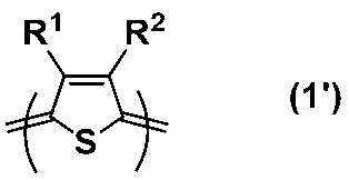
そこで、上記ポリチオフェン誘導体を、還元剤を用いる還元処理に付すと、ポリチオフェン誘導体にキノイド構造が過剰に導入されていても、還元によりキノイド構造が減少し、ポリチオフェン誘導体の有機溶媒に対する溶解性や分散性が向上するため、均質性に優れた薄膜を与える良好な電荷輸送性インク組成物を、安定的に製造することが可能になる。
このような還元剤も還元が適切にされる限り特に制限はないが、例えば、市販品で入手が容易であるアンモニア水、ヒドラジン等が適当である。
また、還元剤の量は、用いる還元剤の量に応じて異なるため一概に規定できないが、処理すべきポリチオフェン誘導体やアミン付加体100質量部に対し、通常、還元が適切にされる観点から、0.1質量部以上であり、過剰な還元剤が残存しないようにする観点から、10質量部以下である。
また、式(1)で表される繰り返し単位を含むポリチオフェン誘導体は、市販品を用いても、チオフェン誘導体などを出発原料とした公知の方法によって重合したものを用いてもよいが、いずれの場合も再沈殿やイオン交換等の方法により精製されたものを用いることが好ましい。精製したものを用いることで、本発明の電荷輸送性インク組成物から得られる薄膜を備えた有機EL素子の特性をより高めることができる。
本発明では、これらの中でも、アミド系溶媒、グリコールエーテル系溶媒およびグリコール系溶媒が好ましく、1,3-ジメチル-2-イミダゾリジノン、ジプロピレングリコールおよびジプロピレングリコールモノメチルエーテルがより好ましい。
なお、これらの有機溶媒は、それぞれ単独で、または2種以上混合して用いることができる。
本発明で用いる金属酸化物ナノ粒子の一次粒子径は、ナノサイズであれば特に限定されるものではないが、再現性よく平坦性に優れた薄膜を得ることを考慮すると、2~150nmが好ましく、3~100nmがより好ましく、5~50nmがより一層好ましい。なお、粒子径は、BET法による窒素吸着等温線を用いた測定値である。
通常の意味での金属としては、特に限定されるものではないが、スズ(Sn)、チタン(Ti)、アルミニウム(Al)、ジルコニウム(Zr)、亜鉛(Zn)、ニオブ(Nb)、タンタル(Ta)およびタングステン(W)からなる群より選択される1種または2種以上を用いることが好ましい。
一方、半金属とは、化学的および/または物理的性質が金属と非金属の中間である元素を意味する。半金属の普遍的な定義は確立されていないが、本発明では、ホウ素(B)、ケイ素(Si)、ゲルマニウム(Ge)、ヒ素(As)、アンチモン(Sb)およびテルル(Te)の計6元素を半金属とする。これらの半金属は、単独で用いても、2種以上を組み合わせて用いてもよく、また通常の意味での金属と組み合わせて用いてもよい。
すなわち、金属酸化物ナノ粒子自体を、電荷輸送性物質等とともに溶媒に混ぜて分散させるよりも、予め金属酸化物ナノ粒子ゾルを調製し、そのゾルを、電荷輸送性物質等が溶媒に溶解または分散した混合物と混ぜることで、金属酸化物ナノ粒子が均一に分散した電荷輸送性インク組成物を再現性よく製造できる。
このような金属酸化物ナノ粒子ゾルは、市販品を用いてもよく、本発明の電荷輸送性インク組成物が含み得る溶媒および金属酸化物ナノ粒子を用いて公知の方法で調製することもできる。
シリカゾルとしては、特に限定されるものではなく、公知のシリカゾルから適宜選択して用いることができる。
市販のシリカゾルは通常、分散液の形態にある。市販のシリカゾルとしては、SiO2ナノ粒子が種々の溶媒、例えば、水、メタノール、メチルエチルケトン、メチルイソブチルケトン、N,N-ジメチルアセトアミド、エチレングリコール、イソプロパノール、メタノール、エチレングリコールモノプロピルエーテル、シクロヘキサノン、酢酸エチル、トルエン、プロピレングリコールモノメチルエーテルアセタート等に分散したものが挙げられる。
特に、本発明においては、分散媒がアルコール系溶、グリコール系溶媒または水であるシリカゾルが好ましく、分散媒がアルコール系溶媒またはグリコール系溶媒であるシリカゾルがより好ましい。アルコール系溶媒又はグリコール系溶媒としては、水溶性のアルコールまたはグリコール系溶媒が好ましく、メタノール、2-プロパノール、エチレングリコールがより好ましい。
本発明の電荷輸送性インク組成物が、ドーパント物質を含む場合、その含有量は、電荷輸送性物質の種類や量等を勘案して適宜設定されるものではあるが、通常、質量比で、電荷輸送性物質1に対して0.1~20.0の範囲である。
これら無機系および有機系のドーパント物質は、1種類単独で用いてもよく、2種類以上組み合わせて用いてもよい。

A2は、ナフタレン環またはアントラセン環を表すが、ナフタレン環が好ましい。
A3は、2~4価のパーフルオロビフェニル基を表し、sは、A1とA3との結合数を示し、2≦s≦4を満たす整数であるが、A3がパーフルオロビフェニルジイル基、好ましくはパーフルオロビフェニル-4,4’-ジイル基であり、かつ、sが2であることが好ましい。
qは、A2に結合するスルホン酸基数を表し、1≦q≦4を満たす整数であるが、2が最適である。
その他、ハロゲン原子、炭素数1~20のアルキル基の例としては上記と同様のものが挙げられるが、ハロゲン原子としては、フッ素原子が好ましい。
なお、パーフルオロアルキル基とは、アルキル基の水素原子全てがフッ素原子に置換された基であり、パーフルオロアルケニル基とは、アルケニル基の水素原子全てがフッ素原子に置換された基である。
特に、ドーパント物質として用いるアリールスルホン酸化合物の分子量は、特に限定されるものではないが、有機溶媒への溶解性を考慮すると、好ましくは2,000以下、より好ましくは1,500以下である。

このようなその他のアミン化合物は、インク組成物に使用する少なくとも一種の溶媒に溶解するものであれば特に限定されず、1種単独であっても、2種以上であってもよい。

特に、1種類のヘテロポリ酸のみを含む場合、その1種類のヘテロポリ酸は、タングステンを含むことが好ましい。すなわち、リンタングステン酸、ケイタングステン酸、リンタングストモリブデン酸等が好ましく、リンタングステン酸、ケイタングステン酸がより好ましい。
すなわち、例えば、一般的には、リンタングステン酸は化学式H3(PW12O40)・nH2Oで示されるが、定量分析において、この式中のP(リン)、O(酸素)またはW(タングステン)の数が多く、または少ないものであっても、それが市販品として入手したもの、あるいは、公知の合成方法に従い適切に合成したものである限り、本発明において用いることができる。この場合、本発明に規定されるヘテロポリ酸の質量とは、合成物や市販品中における純粋なリンタングステン酸の質量(リンタングステン酸含量)ではなく、市販品として入手可能な形態および公知の合成法にて単離可能な形態において、水和水やその他の不純物等を含んだ状態での全質量を意味する。
金属酸化物ナノ粒子を使用する場合は、上記方法において任意のタイミングで当該金属酸化物ナノ粒子の水分散液または有機溶媒分散液を加える方法や、金属酸化物ナノ粒子の水分散液または有機溶媒分散液に、予め準備した式(P1)で表されるアミン化合物および電荷輸送性物質を含む溶液と他の成分またはその溶液とを加える方法が挙げられる。
なお、電荷輸送性物質や金属酸化物ナノ粒子は、共に混ぜられる溶媒の種類や量によっては、混ぜられた際に凝集または沈殿する可能性がある点を留意する。
電荷輸送性インク組成物の調製では、成分が分解したり変質したりしない範囲で、適宜加熱してもよい。
有機EL素子の代表的な構成としては、以下(a)~(f)が挙げられるが、これらに限定されるわけではない。なお、下記構成において、必要に応じて、発光層と陽極の間に電子ブロック層等を、発光層と陰極の間にホール(正孔)ブロック層等を設けることもできる。また、正孔注入層、正孔輸送層あるいは正孔注入輸送層が電子ブロック層等としての機能を兼ね備えていてもよく、電子注入層、電子輸送層あるいは電子注入輸送層がホール(正孔)ブロック層等としての機能を兼ね備えていてもよい。さらに、必要に応じて各層の間に任意の機能層を設けることも可能である。
(a)陽極/正孔注入層/正孔輸送層/発光層/電子輸送層/電子注入層/陰極
(b)陽極/正孔注入層/正孔輸送層/発光層/電子注入輸送層/陰極
(c)陽極/正孔注入輸送層/発光層/電子輸送層/電子注入層/陰極
(d)陽極/正孔注入輸送層/発光層/電子注入輸送層/陰極
(e)陽極/正孔注入層/正孔輸送層/発光層/陰極
(f)陽極/正孔注入輸送層/発光層/陰極
「電子注入層」、「電子輸送層」および「電子注入輸送層」とは、発光層と陰極との間に形成される層であって、電子を陰極から発光層へ輸送する機能を有するものであり、発光層と陰極の間に、電子輸送性材料の層が1層のみ設けられる場合、それが「電子注入輸送層」であり、発光層と陰極の間に、電子輸送性材料の層が2層以上設けられる場合、陰極に近い層が「電子注入層」であり、それ以外の層が「電子輸送層」である。
「発光層」とは、発光機能を有する有機層であって、ドーピングシステムを採用する場合、ホスト材料とドーパント材料を含んでいる。このとき、ホスト材料は、主に電子と正孔の再結合を促し、励起子を発光層内に閉じ込める機能を有し、ドーパント材料は、再結合で得られた励起子を効率的に発光させる機能を有する。燐光素子の場合、ホスト材料は主にドーパントで生成された励起子を発光層内に閉じ込める機能を有する。
陽極基板上に、上記の方法により、上記電荷輸送性インク組成物を用いて正孔注入層を形成する。これを真空蒸着装置内に導入し、正孔輸送層、発光層、電子輸送層/ホールブロック層、電子注入層、陰極金属を順次蒸着する。あるいは、当該方法において蒸着で正孔輸送層と発光層を形成する代わりに、正孔輸送性高分子を含む正孔輸送層形成用組成物と発光性高分子を含む発光層形成用組成物を用いてウェットプロセスによってこれらの層を形成する。なお、必要に応じて、発光層と正孔輸送層との間に電子ブロック層を設けてよい。
なお、金属陽極を構成するその他の金属としては、金、銀、銅、インジウムやこれらの合金等が挙げられるが、これらに限定されるわけではない。
また、蒸着で発光層を形成する場合、発光性ドーパントと共蒸着してもよく、発光性ドーパントとしては、トリス(2-フェニルピリジン)イリジウム(III)(Ir(ppy)3)等の金属錯体や、ルブレン等のナフタセン誘導体、キナクリドン誘導体、ペリレン等の縮合多環芳香族環等が挙げられるが、これらに限定されない。
陰極材料としては、アルミニウム、マグネシウム-銀合金、アルミニウム-リチウム合金等が挙げられるが、これらに限定されない。
電子ブロック層を形成する材料としては、トリス(フェニルピラゾール)イリジウム等が挙げられるが、これに限定されない。
通常、ボトムエミッション構造の素子では、基板側に透明陽極が用いられ、基板側から光が取り出されるのに対し、トップエミッション構造の素子では、金属からなる反射陽極が用いられ、基板と反対方向にある透明電極(陰極)側から光が取り出されることから、例えば陽極材料について言えば、ボトムエミッション構造の素子を製造する際はITO等の透明陽極を、トップエミッション構造の素子を製造する際はAl/Nd等の反射陽極を、それぞれ用いる。
電荷輸送性インク組成物の保存安定性の向上は、吸光度の変化で評価することができる。具体的には、極大吸収(例えば波長620nm)における、大気暴露前の電荷輸送性インク組成物の吸光度をa(初期)、10日間暴露後の電荷輸送性インク組成物の吸光度をa(大気暴露)、大気暴露前後の吸光度の差分(a(初期)-a(大気暴露))をΔaとそれぞれした場合において、吸光度の変化率(%)=Δa/a(初期)の絶対値として、通常10%以下、好ましい態様においては9%以下、より好ましい態様においては8%以下、より一層好ましい態様おいては7%以下、更に好ましい態様においては6%以下である。
電荷輸送性薄膜の平坦性の向上は、平均表面粗さRaで評価することができる。具体的には、基板上に形成した電荷輸送性薄膜を測定範囲を3μm×3μmとして原子間力顕微鏡を用いて測定した場合において、平均表面粗さRa(nm)として、通常2.80nm以下、好ましい態様においては2.70nm以下、より好ましい態様においては2.60nm以下、好ましい態様においては2.50nm以下である。
本発明においては、電荷輸送性薄膜の平均表面粗さ(Ra)は、例えば、パークシステムズ社製 原子間力顕微鏡Park-NX10およびオリンパス(株)製 平均面粗さ測定用カンチレバー OMCL-AC 160TS 10Mを用いて測定することができる。
(2)電荷輸送性薄膜の平均表面粗さ(Ra)の測定:パークシステムズ社製 原子間力顕微鏡Park-NX10およびオリンパス(株)製 平均表面粗さ測定用カンチレバー OMCL-AC 160TS 10M
(3)インク組成物の溶液吸収スペクトル測定:島津サイエンス(株)製、紫外可視近赤外分光光度計UV-3600
(4)有機EL素子の作製:長州産業(株)製、多機能蒸着装置システムC-E2L1G1-N
(5)有機EL素子の輝度等の測定:(株)EHC製、多チャンネルIVL測定装置
[製造例1]
米国特許第8017241号明細書および国際公開第2016/171935号の記載の方法に順次従って、式(1a)で表される繰り返し単位を含むポリマーであるポリチオフェン誘導体のアミン付加体を合成した。

国際公開第2006/025342号に記載の方法に従って、式(b-1)で表されるアリールスルホン酸化合物Aを合成した。

[調製例1]
アリールスルホン酸化合物Aが10質量%含まれる1,3-ジメチル-2-イミダゾリジノン溶液を調製した。上記溶液は、ホットスターラーを用いて、400rpm、50℃で1時間撹拌することで調製した。
水分散のシリカゾルであるST-OS(日産化学(株)製)100gと、ジプロピレングリコールモノメチルエーテル(関東化学(株)製、以下同様)をナスフラスコに入れ、エバポレーターを用いてST-OS中に含まれる水をジプロピレングリコールモノメチルエーテルに置換し、ジプロピレングリコールモノメチルエーテルを分散媒とするシリカゾル(シリカ濃度9.43質量%)を得た。
[実施例1-1]
三角フラスコに1,3-ジメチル-2-イミダゾリジノン3.24g、ジプロピレングリコール(純正化学(株)製、以下同様)5.17gおよびジプロピレングリコールモノメチルエーテル3.55gを入れ、スターラーを用いて室温で30分間撹拌した。その後、調製例1で得られたアリールスルホン酸化合物Aの1,3-ジメチル-2-イミダゾリジノン溶液0.21gを加え、スターラーを用いて室温で30分間撹拌した。
得られた混合物に、製造例1で得られたポリチオフェン誘導体のアミン付加体0.10g、1,3-ジメチル-2-イミダゾリジノン(関東化学(株)製、以下同様)4.75gおよび3-エトキシプロピルアミン(東京化成工業(株)製)0.15gをホットスターラーを用いて80℃で3時間撹拌して得られた溶液のうち1.05gを加え、室温で30分間撹拌した。
次いで、得られた混合物に、調製例2で得られたジプロピレングリコールモノメチルエーテルを分散媒とするシリカゾル1.78gを加え、室温で30分間撹拌した。
最後に、得られた混合物を孔径0.2μmのPPシリンジフィルターでろ過し、電荷輸送性インク組成物を得た。
三角フラスコに1,3-ジメチル-2-イミダゾリジノン3.24g、ジプロピレングリコール5.17gおよびジプロピレングリコールモノメチルエーテル3.55gを入れ、スターラーを用いて室温で30分間撹拌した。その後、調製例1で得られたアリールスルホン酸化合物Aの1,3-ジメチル-2-イミダゾリジノン溶液0.21gを加え、スターラーを用いて室温で30分間撹拌した。
得られた混合物に、製造例1で得られたポリチオフェン誘導体のアミン付加体0.10g、1,3-ジメチル-2-イミダゾリジノン4.75gおよび3-イソプロポキシプロピルアミン(東京化成工業(株)製)0.15gをホットスターラーを用いて80℃で3時間撹拌して得られる混合物のうち1.05gを加え、室温で30分間撹拌した。
次いで、得られた混合物に、調製例2で得られたジプロピレングリコールモノメチルエーテルを分散媒とするシリカゾル1.78gを加え、室温で30分間撹拌した。
最後に、得られた混合物を孔径0.2μmのPPシリンジフィルターでろ過し、電荷輸送性インク組成物を得た。
三角フラスコに1,3-ジメチル-2-イミダゾリジノン3.24g、ジプロピレングリコール5.17gおよびジプロピレングリコールモノメチルエーテル3.55gを入れ、スターラーを用いて室温で30分間撹拌した。その後、調製例1で得られたアリールスルホン酸化合物Aの1,3-ジメチル-2-イミダゾリジノン溶液0.21gを加え、スターラーを用いて室温で30分間撹拌した。
得られた混合物に、製造例1で得られたポリチオフェン誘導体のアミン付加体0.10g、1,3-ジメチル-2-イミダゾリジノン4.75gおよびn-ブチルアミン(東京化成工業(株)製)0.15gをホットスターラーを用いて80℃で3時間撹拌して得られた混合物のうち1.05gを加え、室温で30分間撹拌した。
次いで、得られた混合物に、調製例2で得られたジプロピレングリコールモノメチルエーテルを分散媒とするシリカゾルを1.78g加え、室温で30分間撹拌した。
最後に、得られた混合物を孔径0.2μmのPPシリンジフィルターでろ過し、電荷輸送性インク組成物を得た。
三角フラスコに1,3-ジメチル-2-イミダゾリジノン3.24g、ジプロピレングリコール5.17gおよびジプロピレングリコールモノメチルエーテル3.55gを入れ、スターラーを用いて室温で30分間撹拌した。その後、調製例1で得られたアリールスルホン酸化合物Aの1,3-ジメチル-2-イミダゾリジノン溶液0.21gを加え、スターラーを用いて室温で30分間撹拌した。
得られた混合物に、製造例1で得られたポリチオフェン誘導体のアミン付加体0.10g、1,3-ジメチル-2-イミダゾリジノン4.75gおよびイソアミルアミン(東京化成工業(株)製)0.15gをホットスターラーを用いて80℃で3時間撹拌して得られた混合物のうち1.05gを加え、室温で30分間撹拌した。
次いで、得られた混合物に、調製例2で得られたジプロピレングリコールモノメチルエーテルを分散媒とするシリカゾルを1.78g加え、室温で30分間撹拌した。
最後に、得られた混合物を孔径0.2μmのPPシリンジフィルターでろ過し、電荷輸送性インク組成物を得た。
製造例1で得られたポリチオフェン誘導体のアミン付加体0.10gを、1,3-ジメチル-2-イミダゾリジノン4.75gおよび3-アミノプロパノール(東京化成工業(株)製)0.15gに加え、ホットスターラーを用いて80℃で3時間撹拌したが、ポリチオフェン誘導体のアミン付加体が十分に溶解も分散もせず、電荷輸送性薄膜の形成に使用し得る程度に均一な組成物を調製できなかった。
製造例1で得られたポリチオフェン誘導体のアミン付加体0.10gを、1,3-ジメチル-2-イミダゾリジノン4.75gおよび2-アミノ-1-メトキシブタン(東京化成工業(株)製)0.15gに加え、ホットスターラーを用いて80℃で3時間撹拌したが、ポリチオフェン誘導体のアミン付加体が十分に溶解も分散もせず、電荷輸送性薄膜の形成に使用し得る程度に均一な組成物を調製できなかった。
製造例1で得られたポリチオフェン誘導体のアミン付加体0.10gを、1,3-ジメチル-2-イミダゾリジノン4.75gおよび、ビス(2-エトキシエチル)アミン(東京化成工業(株)製)0.15gに加え、ホットスターラーを用いて80℃で3時間撹拌したが、ポリチオフェン誘導体のアミン付加体が十分に溶解も分散もせず、電荷輸送性薄膜の形成に使用し得る程度に均一な組成物を調製できなかった。
[実施例2-1]
実施例1-1で得られた電荷輸送性インク組成物を、スピンコーターを用いてITO基板に塗布し、大気下、120℃で1分間加熱した後、230℃で15分間加熱し、ITO基板上に厚さ30nmの均一な薄膜を形成した。
なお、ITO基板としては、インジウム錫酸化物(ITO)がガラス基板上に膜厚50nmでパターニングされた、25mm×25mm×0.7tのガラス基板を用い、使用前にO2プラズマ洗浄装置(150W、30秒間)によって表面上の不純物を除去した。
実施例1-1の電荷輸送性インク組成物の代わりに、実施例1-2、比較例1-1~1-2で得られた電荷輸送性インク組成物をそれぞれ用いた以外は、実施例2-1と同様の方法で、ITO基板上に厚さ30nmの均一な薄膜を形成した。

[実施例3-1]
実施例1-1で得られた電荷輸送性インク組成物0.2gを、1,3-ジメチル-2-イミダゾリジノン4.14g、ジプロピレングリコール4.83gおよびジプロピレングリコールモノメチルエーテル4.83gと混合し、得られた混合物の吸収スペクトル測定を行った。
次いで、実施例1-1で得られた電荷輸送性インク組成物3.0gを、20mLの容量のガラス製バイアル瓶に加え、バイアル瓶の蓋を開放した状態で、大気下、室温で10日間大気暴露した。大気暴露した電荷輸送性インク組成物0.2gを、1,3-ジメチル-2-イミダゾリジノン4.14g、ジプロピレングリコール4.83gおよびジプロピレングリコールモノメチルエーテル4.83gと混合し、得られた混合物の吸収スペクトル測定を行った。
なお、吸収スペクトル測定には、光路長1cmの石英製のセルを用いた。
実施例1-1で得られた電荷輸送性インク組成物の代わりに、実施例1-2、比較例1-1~1-2で得られた電荷輸送性インク組成物をそれぞれ用いた以外は、実施例3-1と同法の方法で、収スペクトル測定を行った。

[実施例4-1]
実施例1-1で得られた電荷輸送性インク組成物を、スピンコーターを用いてITO基板に塗布し、大気下、120℃で1分間加熱した後、230℃で15分間加熱し、ITO基板上に厚さ30nmの均一な電荷輸送性薄膜を形成した。
なお、ITO基板としては、パターニングされた厚さ150nmのITO膜が表面に形成された、25mm×25mm×0.7tのガラス基板を用い、使用前にO2プラズマ洗浄装置(150W、30秒間)によって表面上の不純物を除去した。
次いで、ITO基板に形成された電荷輸送性薄膜上に、蒸着装置(真空度1.0×10⁻⁵Pa)を用いて、α-NPD(N,N’-ジ(1-ナフチル)-N,N’-ジフェニルベンジジン)を0.2nm/秒にて30nm成膜した。
α-NPDの膜の上に、関東化学(株)製の電子ブロック材料HTEB-01を10nm成膜し、更にその上に、新日鉄住金化学(株)製の発光層ホスト材料NS60と発光層ドーパント材料Ir(ppy)3を共蒸着した。共蒸着は、Ir(ppy)3の濃度が6%になるように蒸着レートをコントロールし、40nm積層させた。次いで、Alq3、フッ化リチウムおよびアルミニウムの薄膜を順次積層して、有機EL素子を得た。この際、蒸着レートは、Alq3およびアルミニウムについては0.2nm/秒、フッ化リチウムについては0.02nm/秒の条件でそれぞれ行い、膜厚は、それぞれ20nm、0.5nmおよび80nmとした。
実施例1-1で得られた電荷輸送性インク組成物の代わりに、実施例1-2で得られた電荷輸送性インク組成物を用いた以外は、実施例4-1と同様の方法で有機EL素子を得た。

Claims (12)
- 下記式(P1)で表されるアミン化合物と、電荷輸送性物質と、有機溶媒とを含むことを特徴とする電荷輸送性インク組成物。

- 上記Rmが、炭素数1~20のアルキル基であり、上記Rnが、炭素数1~20のアルキレン基である請求項1記載の電荷輸送性インク組成物。
- 上記電荷輸送性物質が、下記式(1)で表される繰り返し単位を含むポリチオフェン誘導体またはそのアミン付加体である請求項1または2記載の電荷輸送性インク組成物。
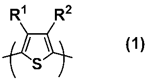
- 上記R1が、スルホン酸基であり、上記R2が、炭素数1~40のアルコキシ基もしくは-O-[Z-O]p-Reである、または上記R1およびR2が結合して形成される-O-Y-O-である請求項3記載の電荷輸送性インク組成物。
- さらに、ドーパント物質を含む請求項1~4のいずれか1項記載の電荷輸送性インク組成物。
- 上記ドーパント物質が、アリールスルホン酸化合物およびヘテロポリ酸化合物よりなる群から選ばれる少なくとも1種を含む請求項5記載の電荷輸送性インク組成物。
- さらに、金属酸化物ナノ粒子を含む請求項1~6のいずれか1項記載の電荷輸送性インク組成物。
- 請求項1~7のいずれか1項記載の電荷輸送性インク組成物から得られる電荷輸送性薄膜。
- 請求項8記載の電荷輸送性薄膜を有する電子素子。
- 有機エレクトロルミネッセンス素子である請求項9記載の電子素子。
- アミン化合物と、電荷輸送性物質と、有機溶媒とを含む電荷輸送性インク組成物の保存安定性の向上方法であって、
上記アミン化合物として、下記式(P1)で表されるアミン化合物を用いることを特徴とする電荷輸送性インク組成物の保存安定性の向上方法。

- アミン化合物と、電荷輸送性物質と、有機溶媒とを含む電荷輸送性インク組成物から得られる電荷輸送性薄膜の平坦性の向上方法であって、
上記アミン化合物として、下記式(P1)で表されるアミン化合物を用いることを特徴とする電電荷輸送性薄膜の平坦性の向上方法。

Priority Applications (3)
| Application Number | Priority Date | Filing Date | Title |
|---|---|---|---|
| KR1020237030032A KR20230147645A (ko) | 2021-02-25 | 2022-02-22 | 전하 수송성 잉크 조성물 |
| JP2023502422A JP7736057B2 (ja) | 2021-02-25 | 2022-02-22 | 電荷輸送性インク組成物 |
| CN202280016523.8A CN116888223B (zh) | 2021-02-25 | 2022-02-22 | 电荷传输性墨组合物 |
Applications Claiming Priority (2)
| Application Number | Priority Date | Filing Date | Title |
|---|---|---|---|
| JP2021-029226 | 2021-02-25 | ||
| JP2021029226 | 2021-02-25 |
Publications (1)
| Publication Number | Publication Date |
|---|---|
| WO2022181587A1 true WO2022181587A1 (ja) | 2022-09-01 |
Family
ID=83048156
Family Applications (1)
| Application Number | Title | Priority Date | Filing Date |
|---|---|---|---|
| PCT/JP2022/007152 Ceased WO2022181587A1 (ja) | 2021-02-25 | 2022-02-22 | 電荷輸送性インク組成物 |
Country Status (5)
| Country | Link |
|---|---|
| JP (1) | JP7736057B2 (ja) |
| KR (1) | KR20230147645A (ja) |
| CN (1) | CN116888223B (ja) |
| TW (1) | TWI911392B (ja) |
| WO (1) | WO2022181587A1 (ja) |
Cited By (1)
| Publication number | Priority date | Publication date | Assignee | Title |
|---|---|---|---|---|
| JP2024073908A (ja) * | 2022-11-18 | 2024-05-30 | 国立大学法人千葉大学 | 金属光沢を発現する膜、その膜を生成する水溶性塗料およびそれらに用いることができる新規なチオフェン共重合体 |
Citations (3)
| Publication number | Priority date | Publication date | Assignee | Title |
|---|---|---|---|---|
| JP2004204114A (ja) * | 2002-12-26 | 2004-07-22 | Dainippon Printing Co Ltd | インクジェット用インク組成物 |
| JP4573363B1 (ja) * | 2010-06-01 | 2010-11-04 | テイカ株式会社 | 有機溶剤系導電性高分子分散液の製造方法およびその応用 |
| JP2018523722A (ja) * | 2015-07-17 | 2018-08-23 | 日産化学株式会社 | 有機電子デバイスに使用するのに適した金属ナノ粒子を含有する非水性インク組成物 |
Family Cites Families (15)
| Publication number | Priority date | Publication date | Assignee | Title |
|---|---|---|---|---|
| US7317047B2 (en) * | 2002-09-24 | 2008-01-08 | E.I. Du Pont De Nemours And Company | Electrically conducting organic polymer/nanoparticle composites and methods for use thereof |
| TWI326297B (en) * | 2005-03-21 | 2010-06-21 | Inktec Co Ltd | Conductive ink composition and preparing method thereof |
| JP5300341B2 (ja) * | 2008-06-20 | 2013-09-25 | キヤノン株式会社 | 電子写真感光体、プロセスカートリッジ及び電子写真装置 |
| JP2011114322A (ja) * | 2009-11-30 | 2011-06-09 | Fujifilm Corp | 電荷輸送性化合物、それを用いた電荷輸送膜、有機電界発光素子、電子写真感光体、電荷輸送膜の製造方法及び新規電荷輸送性化合物。 |
| JP2012254976A (ja) * | 2011-05-17 | 2012-12-27 | Tosoh Corp | 電荷輸送層添加剤およびそれを用いた有機薄膜電子デバイス |
| WO2014132834A1 (ja) * | 2013-02-26 | 2014-09-04 | 日産化学工業株式会社 | 電荷輸送性ワニス |
| JP2014209473A (ja) * | 2013-03-28 | 2014-11-06 | 日本合成化学工業株式会社 | 酸化亜鉛を主成分とする独立透明導電膜とその製造方法、それを含む多層構造体の製造方法、および多層構造体。 |
| JP6511657B2 (ja) * | 2014-09-03 | 2019-05-15 | 日本放送協会 | 有機金属錯体、有機エレクトロルミネッセンス素子およびその製造方法、表示装置、照明装置、有機薄膜太陽電池 |
| JP2018011010A (ja) * | 2016-07-15 | 2018-01-18 | 日立化成株式会社 | 電荷輸送性材料、インク組成物、及び有機エレクトロニクス素子 |
| KR102338021B1 (ko) * | 2016-11-01 | 2021-12-10 | 도레이 카부시키가이샤 | 터치 패널, 터치 패널의 제조 방법 |
| KR102564836B1 (ko) | 2017-01-18 | 2023-08-09 | 닛산 가가쿠 가부시키가이샤 | 잉크 조성물 |
| JP7088009B2 (ja) * | 2017-01-18 | 2022-06-21 | 日産化学株式会社 | スルホン化共役ポリマーを含有するインク組成物 |
| JP6547792B2 (ja) * | 2017-06-12 | 2019-07-24 | 日産化学株式会社 | 電荷輸送性ワニス |
| US20210122928A1 (en) * | 2018-07-04 | 2021-04-29 | Nissan Chemical Corporation | Charge-transporting composition |
| WO2020027259A1 (ja) * | 2018-08-03 | 2020-02-06 | 日産化学株式会社 | 電荷輸送性ワニス |
-
2022
- 2022-02-22 WO PCT/JP2022/007152 patent/WO2022181587A1/ja not_active Ceased
- 2022-02-22 KR KR1020237030032A patent/KR20230147645A/ko active Pending
- 2022-02-22 JP JP2023502422A patent/JP7736057B2/ja active Active
- 2022-02-22 CN CN202280016523.8A patent/CN116888223B/zh active Active
- 2022-02-24 TW TW111106704A patent/TWI911392B/zh active
Patent Citations (3)
| Publication number | Priority date | Publication date | Assignee | Title |
|---|---|---|---|---|
| JP2004204114A (ja) * | 2002-12-26 | 2004-07-22 | Dainippon Printing Co Ltd | インクジェット用インク組成物 |
| JP4573363B1 (ja) * | 2010-06-01 | 2010-11-04 | テイカ株式会社 | 有機溶剤系導電性高分子分散液の製造方法およびその応用 |
| JP2018523722A (ja) * | 2015-07-17 | 2018-08-23 | 日産化学株式会社 | 有機電子デバイスに使用するのに適した金属ナノ粒子を含有する非水性インク組成物 |
Cited By (1)
| Publication number | Priority date | Publication date | Assignee | Title |
|---|---|---|---|---|
| JP2024073908A (ja) * | 2022-11-18 | 2024-05-30 | 国立大学法人千葉大学 | 金属光沢を発現する膜、その膜を生成する水溶性塗料およびそれらに用いることができる新規なチオフェン共重合体 |
Also Published As
| Publication number | Publication date |
|---|---|
| JP7736057B2 (ja) | 2025-09-09 |
| CN116888223A (zh) | 2023-10-13 |
| KR20230147645A (ko) | 2023-10-23 |
| JPWO2022181587A1 (ja) | 2022-09-01 |
| CN116888223B (zh) | 2026-03-20 |
| TW202302775A (zh) | 2023-01-16 |
| TWI911392B (zh) | 2026-01-11 |
Similar Documents
| Publication | Publication Date | Title |
|---|---|---|
| JP7392644B2 (ja) | 電荷輸送性組成物 | |
| US20090269688A1 (en) | Charge-transporting varnish | |
| JP2023171836A (ja) | 電荷輸送性組成物 | |
| JP7852639B2 (ja) | フッ素化アリールスルホン酸ポリマー化合物およびその利用 | |
| JP7736057B2 (ja) | 電荷輸送性インク組成物 | |
| KR102836344B1 (ko) | 전하수송성 바니시 | |
| KR20230164092A (ko) | 전하 수송성 바니시 | |
| TWI894324B (zh) | 附有機機能膜之基板的製造方法、電子元件之製造方法及噴墨法用墨水 | |
| WO2023189399A1 (ja) | ポリマーおよびその利用 | |
| JP6547792B2 (ja) | 電荷輸送性ワニス | |
| WO2024241889A1 (ja) | 電荷輸送性ワニス |
Legal Events
| Date | Code | Title | Description |
|---|---|---|---|
| 121 | Ep: the epo has been informed by wipo that ep was designated in this application |
Ref document number: 22759623 Country of ref document: EP Kind code of ref document: A1 |
|
| ENP | Entry into the national phase |
Ref document number: 2023502422 Country of ref document: JP Kind code of ref document: A |
|
| WWE | Wipo information: entry into national phase |
Ref document number: 202280016523.8 Country of ref document: CN |
|
| ENP | Entry into the national phase |
Ref document number: 20237030032 Country of ref document: KR Kind code of ref document: A |
|
| WWE | Wipo information: entry into national phase |
Ref document number: 1020237030032 Country of ref document: KR |
|
| NENP | Non-entry into the national phase |
Ref country code: DE |
|
| 122 | Ep: pct application non-entry in european phase |
Ref document number: 22759623 Country of ref document: EP Kind code of ref document: A1 |