WO2022181542A1 - 半導体デバイスの製造方法、半導体デバイスおよび半導体装置 - Google Patents
半導体デバイスの製造方法、半導体デバイスおよび半導体装置 Download PDFInfo
- Publication number
- WO2022181542A1 WO2022181542A1 PCT/JP2022/006935 JP2022006935W WO2022181542A1 WO 2022181542 A1 WO2022181542 A1 WO 2022181542A1 JP 2022006935 W JP2022006935 W JP 2022006935W WO 2022181542 A1 WO2022181542 A1 WO 2022181542A1
- Authority
- WO
- WIPO (PCT)
- Prior art keywords
- semiconductor device
- support
- laminate
- substrate
- manufacturing
- Prior art date
- Legal status (The legal status is an assumption and is not a legal conclusion. Google has not performed a legal analysis and makes no representation as to the accuracy of the status listed.)
- Ceased
Links
Images












Classifications
-
- H—ELECTRICITY
- H01—ELECTRIC ELEMENTS
- H01S—DEVICES USING THE PROCESS OF LIGHT AMPLIFICATION BY STIMULATED EMISSION OF RADIATION [LASER] TO AMPLIFY OR GENERATE LIGHT; DEVICES USING STIMULATED EMISSION OF ELECTROMAGNETIC RADIATION IN WAVE RANGES OTHER THAN OPTICAL
- H01S5/00—Semiconductor lasers
- H01S5/02—Structural details or components not essential to laser action
- H01S5/022—Mountings; Housings
- H01S5/023—Mount members, e.g. sub-mount members
- H01S5/02315—Support members, e.g. bases or carriers
-
- H—ELECTRICITY
- H10—SEMICONDUCTOR DEVICES; ELECTRIC SOLID-STATE DEVICES NOT OTHERWISE PROVIDED FOR
- H10H—INORGANIC LIGHT-EMITTING SEMICONDUCTOR DEVICES HAVING POTENTIAL BARRIERS
- H10H20/00—Individual inorganic light-emitting semiconductor devices having potential barriers, e.g. light-emitting diodes [LED]
- H10H20/80—Constructional details
- H10H20/81—Bodies
- H10H20/819—Bodies characterised by their shape, e.g. curved or truncated substrates
-
- H—ELECTRICITY
- H01—ELECTRIC ELEMENTS
- H01S—DEVICES USING THE PROCESS OF LIGHT AMPLIFICATION BY STIMULATED EMISSION OF RADIATION [LASER] TO AMPLIFY OR GENERATE LIGHT; DEVICES USING STIMULATED EMISSION OF ELECTROMAGNETIC RADIATION IN WAVE RANGES OTHER THAN OPTICAL
- H01S5/00—Semiconductor lasers
- H01S5/02—Structural details or components not essential to laser action
- H01S5/0201—Separation of the wafer into individual elements, e.g. by dicing, cleaving, etching or directly during growth
- H01S5/0202—Cleaving
-
- H—ELECTRICITY
- H01—ELECTRIC ELEMENTS
- H01S—DEVICES USING THE PROCESS OF LIGHT AMPLIFICATION BY STIMULATED EMISSION OF RADIATION [LASER] TO AMPLIFY OR GENERATE LIGHT; DEVICES USING STIMULATED EMISSION OF ELECTROMAGNETIC RADIATION IN WAVE RANGES OTHER THAN OPTICAL
- H01S5/00—Semiconductor lasers
- H01S5/02—Structural details or components not essential to laser action
- H01S5/0206—Substrates, e.g. growth, shape, material, removal or bonding
- H01S5/0215—Bonding to the substrate
- H01S5/0216—Bonding to the substrate using an intermediate compound, e.g. a glue or solder
-
- H—ELECTRICITY
- H01—ELECTRIC ELEMENTS
- H01S—DEVICES USING THE PROCESS OF LIGHT AMPLIFICATION BY STIMULATED EMISSION OF RADIATION [LASER] TO AMPLIFY OR GENERATE LIGHT; DEVICES USING STIMULATED EMISSION OF ELECTROMAGNETIC RADIATION IN WAVE RANGES OTHER THAN OPTICAL
- H01S5/00—Semiconductor lasers
- H01S5/02—Structural details or components not essential to laser action
- H01S5/022—Mountings; Housings
- H01S5/0225—Out-coupling of light
-
- H—ELECTRICITY
- H01—ELECTRIC ELEMENTS
- H01S—DEVICES USING THE PROCESS OF LIGHT AMPLIFICATION BY STIMULATED EMISSION OF RADIATION [LASER] TO AMPLIFY OR GENERATE LIGHT; DEVICES USING STIMULATED EMISSION OF ELECTROMAGNETIC RADIATION IN WAVE RANGES OTHER THAN OPTICAL
- H01S5/00—Semiconductor lasers
- H01S5/02—Structural details or components not essential to laser action
- H01S5/022—Mountings; Housings
- H01S5/0235—Method for mounting laser chips
- H01S5/02355—Fixing laser chips on mounts
-
- H—ELECTRICITY
- H01—ELECTRIC ELEMENTS
- H01S—DEVICES USING THE PROCESS OF LIGHT AMPLIFICATION BY STIMULATED EMISSION OF RADIATION [LASER] TO AMPLIFY OR GENERATE LIGHT; DEVICES USING STIMULATED EMISSION OF ELECTROMAGNETIC RADIATION IN WAVE RANGES OTHER THAN OPTICAL
- H01S5/00—Semiconductor lasers
- H01S5/02—Structural details or components not essential to laser action
- H01S5/022—Mountings; Housings
- H01S5/0235—Method for mounting laser chips
- H01S5/02355—Fixing laser chips on mounts
- H01S5/0237—Fixing laser chips on mounts by soldering
-
- H—ELECTRICITY
- H01—ELECTRIC ELEMENTS
- H01S—DEVICES USING THE PROCESS OF LIGHT AMPLIFICATION BY STIMULATED EMISSION OF RADIATION [LASER] TO AMPLIFY OR GENERATE LIGHT; DEVICES USING STIMULATED EMISSION OF ELECTROMAGNETIC RADIATION IN WAVE RANGES OTHER THAN OPTICAL
- H01S5/00—Semiconductor lasers
- H01S5/02—Structural details or components not essential to laser action
- H01S5/028—Coatings ; Treatment of the laser facets, e.g. etching, passivation layers or reflecting layers
- H01S5/0287—Facet reflectivity
-
- H—ELECTRICITY
- H01—ELECTRIC ELEMENTS
- H01S—DEVICES USING THE PROCESS OF LIGHT AMPLIFICATION BY STIMULATED EMISSION OF RADIATION [LASER] TO AMPLIFY OR GENERATE LIGHT; DEVICES USING STIMULATED EMISSION OF ELECTROMAGNETIC RADIATION IN WAVE RANGES OTHER THAN OPTICAL
- H01S5/00—Semiconductor lasers
- H01S5/04—Processes or apparatus for excitation, e.g. pumping, e.g. by electron beams
- H01S5/042—Electrical excitation ; Circuits therefor
- H01S5/0425—Electrodes, e.g. characterised by the structure
- H01S5/04256—Electrodes, e.g. characterised by the structure characterised by the configuration
- H01S5/04257—Electrodes, e.g. characterised by the structure characterised by the configuration having positive and negative electrodes on the same side of the substrate
-
- H—ELECTRICITY
- H01—ELECTRIC ELEMENTS
- H01S—DEVICES USING THE PROCESS OF LIGHT AMPLIFICATION BY STIMULATED EMISSION OF RADIATION [LASER] TO AMPLIFY OR GENERATE LIGHT; DEVICES USING STIMULATED EMISSION OF ELECTROMAGNETIC RADIATION IN WAVE RANGES OTHER THAN OPTICAL
- H01S5/00—Semiconductor lasers
- H01S5/30—Structure or shape of the active region; Materials used for the active region
- H01S5/32—Structure or shape of the active region; Materials used for the active region comprising PN junctions, e.g. hetero- or double- heterostructures
- H01S5/323—Structure or shape of the active region; Materials used for the active region comprising PN junctions, e.g. hetero- or double- heterostructures in AIIIBV compounds, e.g. AlGaAs-laser, InP-based laser
-
- H—ELECTRICITY
- H10—SEMICONDUCTOR DEVICES; ELECTRIC SOLID-STATE DEVICES NOT OTHERWISE PROVIDED FOR
- H10H—INORGANIC LIGHT-EMITTING SEMICONDUCTOR DEVICES HAVING POTENTIAL BARRIERS
- H10H20/00—Individual inorganic light-emitting semiconductor devices having potential barriers, e.g. light-emitting diodes [LED]
- H10H20/80—Constructional details
-
- H—ELECTRICITY
- H10—SEMICONDUCTOR DEVICES; ELECTRIC SOLID-STATE DEVICES NOT OTHERWISE PROVIDED FOR
- H10H—INORGANIC LIGHT-EMITTING SEMICONDUCTOR DEVICES HAVING POTENTIAL BARRIERS
- H10H20/00—Individual inorganic light-emitting semiconductor devices having potential barriers, e.g. light-emitting diodes [LED]
- H10H20/80—Constructional details
- H10H20/85—Packages
- H10H20/857—Interconnections, e.g. lead-frames, bond wires or solder balls
-
- H—ELECTRICITY
- H01—ELECTRIC ELEMENTS
- H01S—DEVICES USING THE PROCESS OF LIGHT AMPLIFICATION BY STIMULATED EMISSION OF RADIATION [LASER] TO AMPLIFY OR GENERATE LIGHT; DEVICES USING STIMULATED EMISSION OF ELECTROMAGNETIC RADIATION IN WAVE RANGES OTHER THAN OPTICAL
- H01S2304/00—Special growth methods for semiconductor lasers
- H01S2304/12—Pendeo epitaxial lateral overgrowth [ELOG], e.g. for growing GaN based blue laser diodes
-
- H—ELECTRICITY
- H01—ELECTRIC ELEMENTS
- H01S—DEVICES USING THE PROCESS OF LIGHT AMPLIFICATION BY STIMULATED EMISSION OF RADIATION [LASER] TO AMPLIFY OR GENERATE LIGHT; DEVICES USING STIMULATED EMISSION OF ELECTROMAGNETIC RADIATION IN WAVE RANGES OTHER THAN OPTICAL
- H01S5/00—Semiconductor lasers
- H01S5/02—Structural details or components not essential to laser action
- H01S5/022—Mountings; Housings
- H01S5/0233—Mounting configuration of laser chips
- H01S5/0234—Up-side down mountings, e.g. Flip-chip, epi-side down mountings or junction down mountings
-
- H—ELECTRICITY
- H01—ELECTRIC ELEMENTS
- H01S—DEVICES USING THE PROCESS OF LIGHT AMPLIFICATION BY STIMULATED EMISSION OF RADIATION [LASER] TO AMPLIFY OR GENERATE LIGHT; DEVICES USING STIMULATED EMISSION OF ELECTROMAGNETIC RADIATION IN WAVE RANGES OTHER THAN OPTICAL
- H01S5/00—Semiconductor lasers
- H01S5/20—Structure or shape of the semiconductor body to guide the optical wave ; Confining structures perpendicular to the optical axis, e.g. index or gain guiding, stripe geometry, broad area lasers, gain tailoring, transverse or lateral reflectors, special cladding structures, MQW barrier reflection layers
- H01S5/22—Structure or shape of the semiconductor body to guide the optical wave ; Confining structures perpendicular to the optical axis, e.g. index or gain guiding, stripe geometry, broad area lasers, gain tailoring, transverse or lateral reflectors, special cladding structures, MQW barrier reflection layers having a ridge or stripe structure
-
- H—ELECTRICITY
- H01—ELECTRIC ELEMENTS
- H01S—DEVICES USING THE PROCESS OF LIGHT AMPLIFICATION BY STIMULATED EMISSION OF RADIATION [LASER] TO AMPLIFY OR GENERATE LIGHT; DEVICES USING STIMULATED EMISSION OF ELECTROMAGNETIC RADIATION IN WAVE RANGES OTHER THAN OPTICAL
- H01S5/00—Semiconductor lasers
- H01S5/30—Structure or shape of the active region; Materials used for the active region
- H01S5/34—Structure or shape of the active region; Materials used for the active region comprising quantum well or superlattice structures, e.g. single quantum well [SQW] lasers, multiple quantum well [MQW] lasers or graded index separate confinement heterostructure [GRINSCH] lasers
- H01S5/343—Structure or shape of the active region; Materials used for the active region comprising quantum well or superlattice structures, e.g. single quantum well [SQW] lasers, multiple quantum well [MQW] lasers or graded index separate confinement heterostructure [GRINSCH] lasers in AIIIBV compounds, e.g. AlGaAs-laser, InP-based laser
- H01S5/34333—Structure or shape of the active region; Materials used for the active region comprising quantum well or superlattice structures, e.g. single quantum well [SQW] lasers, multiple quantum well [MQW] lasers or graded index separate confinement heterostructure [GRINSCH] lasers in AIIIBV compounds, e.g. AlGaAs-laser, InP-based laser with a well layer based on Ga(In)N or Ga(In)P, e.g. blue laser
-
- H—ELECTRICITY
- H01—ELECTRIC ELEMENTS
- H01S—DEVICES USING THE PROCESS OF LIGHT AMPLIFICATION BY STIMULATED EMISSION OF RADIATION [LASER] TO AMPLIFY OR GENERATE LIGHT; DEVICES USING STIMULATED EMISSION OF ELECTROMAGNETIC RADIATION IN WAVE RANGES OTHER THAN OPTICAL
- H01S5/00—Semiconductor lasers
- H01S5/40—Arrangement of two or more semiconductor lasers, not provided for in groups H01S5/02 - H01S5/30
- H01S5/4025—Array arrangements, e.g. constituted by discrete laser diodes or laser bar
- H01S5/4031—Edge-emitting structures
-
- H—ELECTRICITY
- H10—SEMICONDUCTOR DEVICES; ELECTRIC SOLID-STATE DEVICES NOT OTHERWISE PROVIDED FOR
- H10H—INORGANIC LIGHT-EMITTING SEMICONDUCTOR DEVICES HAVING POTENTIAL BARRIERS
- H10H20/00—Individual inorganic light-emitting semiconductor devices having potential barriers, e.g. light-emitting diodes [LED]
- H10H20/01—Manufacture or treatment
- H10H20/036—Manufacture or treatment of packages
- H10H20/0364—Manufacture or treatment of packages of interconnections
Definitions
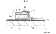
- the laminate 10 When the laminate 10 has a single-sided electrode structure (see FIG. 3A), the laminate 10 is removed from the second semiconductor layer 13 side until the first semiconductor layer 11 is exposed.
- An n-type electrode 14 may be arranged on the surface.
- both the surface of the first semiconductor layer 11 connected to the n-type electrode 14 and the surface of the second semiconductor layer 13 connected to the p-type electrode 15 are the (0001) planes of the GaN-based semiconductor. becomes possible.
- one surface of the semiconductor layer is the (0001) plane and the other surface is the ( A double-sided electrode structure in which a p-type electrode is brought into contact with one surface that is the (0001) surface and an n-type electrode is brought into contact with the other surface that is the (000-1) surface while growing so as to be the (000-1) surface. good too.
- a current flows laterally between the p-type electrode and the n-type electrode. increases, and the driving voltage increases when the current path is longer than in the double-sided electrode structure, but this can be avoided.
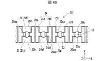
- the first support 20 has a top surface 20a, a first side surface 20b and a second side surface 20c.
- the top surface 20 a , the first side surface 20 b and the second side surface 20 c are surfaces extending in the longitudinal direction of the first support 20 .
- the first side surface 20b continues to the top surface 20a.
- the second side surface 20c continues to the top surface 20a and is located on the opposite side of the first side surface 20b.
- the plurality of laminates 10 are arranged between the plurality of third recesses 31a and the plurality of fourth recesses 31b.
- the first cavity surface 10a and the second cavity surface 10b of each laminate 10 can be completely exposed between the first support 20 and the second support 30 .
- the laminate 10 is excellent in luminous efficiency, Moreover, it is possible to obtain a laminate having excellent reliability.
- the plurality of laminates 10 are arranged on the partially narrowed portion of the second support 30, the second support 30 as a whole has high mechanical strength and excellent handling properties. can be
- the second support 30 used in the formation step S3 may be removed, and only the first support 20 on which the multiple laminates 10 are arranged may be cut.
- the second support 30 may be reused in the next formation step S3.
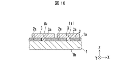
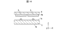
- the ELO method is used to grow the semiconductor element layer 3, which is the precursor of the plurality of laminates 10, from the growth region 1a1 of the underlying substrate 1 to the linear portion 2a of the mask 2, as shown in FIG. Vapor-phase growth is applied to the top.
- Vapor-phase growth is applied to the top.
- HVPE Hydride Vapor Phase Epitaxy
- MOCVD metal organic chemical vapor deposition
- MBE molecular beam vapor deposition
- a plurality of recesses 41 are formed in the first support substrate 4, as shown in FIG. 12, for example.
- the plurality of recesses 41 are opened on one main surface 4 a of the first support substrate 4 and recessed in the thickness direction of the first support substrate 4 .
- the plurality of recesses 41 are arranged in a matrix in a third direction (vertical direction in FIG. 12) and in a fourth direction (horizontal direction in FIG. 12) intersecting the third direction when viewed in a direction orthogonal to one main surface 4a. are arranged in
- the opening shape of the plurality of recesses 41 may be rectangular, square, hexagonal, or any other shape.
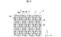
- an external force is applied so as to peel off the semiconductor element layer 3 integrated with the first supporting substrate 4 from the underlying substrate 1, thereby removing the semiconductor element layer 3 from one main surface of the underlying substrate 1. Pull up from 1a. Thereby, the semiconductor element layer 3 can be transferred to the first support substrate 4 as shown in FIG. 15, for example.
- the manufacturing efficiency of semiconductor devices can be further improved.
- the method of manufacturing a semiconductor device described above is particularly effective when the size of the laminate 10 is too small to handle individually.
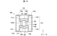
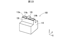
- the substrate 110 may have wiring 114 disposed on the top surface 110a, as shown in FIG. 18, for example.
- the wiring 114 may include a first wiring 114a and a second wiring 114b.
- the first wiring 114a and the second wiring 114b may be arranged apart from each other.
- the first wiring 114a is a joining member 114a electrically connected to the n-type electrode of the laminate 120. 1 may be included.
- the second wiring 114b may include a joining member 114b1 electrically connected to the p-type electrode of the laminate 120.
- an insulating layer may be placed on the upper surface 110a of the substrate 110 and the wiring 114 may be placed on the insulating layer. As a result, short-circuiting between the wirings 114 can be suppressed, so that the semiconductor device can be operated normally.
- the wiring 114 may have a metal layer made of Au, Ti, Ni, or the like, for example.
- the wiring 114 may consist of a single metal layer or may consist of multiple metal layers. When the wiring 114 is composed of multiple metal layers, the outermost surface may be a metal layer composed of Au. Corrosion of the wiring 114 can thereby be suppressed.
- Joining members 114a1, 114b1 is a conductive bonding material such as solder.
- the joining members 114a1 and 114b1 may be solder such as AuSi and AuSn, for example.
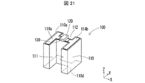
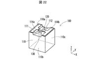
- the semiconductor device 100 has a configuration in which the first recess 111 tapers toward the first side surface 110b and the second recess 112 tapers toward the second side 110c. There may be.
- the semiconductor device 100 shown in FIG. 22 the light extraction efficiency can be improved, and the dielectric layer 130 can be formed satisfactorily.
- the wiring 114 can be easily arranged.
- the mechanical strength of the substrate 110 can be improved, the reliability of the semiconductor device 100 can be improved.
- a plurality of semiconductor devices 100 may be combined to form a composite semiconductor device 200.
- FIG. A composite semiconductor device 200 may be fabricated by combining a plurality of semiconductor devices 100 .
- the composite semiconductor device 200 may be produced by dividing the first support 20 such that one piece of the first support 20 includes a plurality of laminates 10 in the dividing step S4. In this case, the alignment accuracy of the plurality of semiconductor devices 100 in the composite semiconductor device 200 can be increased, which is advantageous when combining the composite semiconductor device 200 with another optical member.
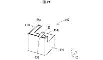
- the bottom surface 110d of the substrate 110 may be connected to the mounting surface of the package 300, and the second side surface 110c of the substrate 110 may be connected to the mounting surface of the package 300.
- the semiconductor device 400 may have photodiodes arranged in the concave portions 111 and 112 of the substrate 110 .
- the photodiode may be configured to detect light emitted from the first cavity surface 120a, or may be configured to detect light leaked from the second cavity surface 120b. As a result, it is possible to control the driving current supplied to the stacked body 120 based on the detection result of the photodiode, so the reliability of the semiconductor device 400 can be improved.
- the first laser body L1 is arranged so that the direction orthogonal to the cavity length direction of the first laser body and the width direction (Y direction) of the first region M1 intersect.
- the second laser body L2 is arranged so that the direction orthogonal to the cavity length direction of the second laser body and the width direction (Y direction) of the second region M2 intersect.
- the cavity length direction of the first laser body L1 may be parallel to the width direction of the first region M1, and the cavity length direction of the second laser body L2 may be parallel to the width direction of the second region M2.
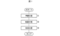
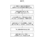
- FIG. 32 is a flow chart showing the method for manufacturing a semiconductor device according to this embodiment.
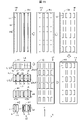
- FIG. 33 is a plan view showing the method of manufacturing the semiconductor device according to this embodiment.
- BS substrate for crystal growth
- a step of forming a two-dimensional laser substrate LF (a step of forming a two-dimensional laser substrate LF), and a step of obtaining a one-dimensional laser substrate LK (including first and second laser bodies L1 and L2) by dividing the two-dimensional laser substrate LF.
- a step of forming the first dielectric layers 7F and 7S (for example, reflector films) (the laser substrate LK may be inverted to form the second dielectric layers 8F and 8S); and a step of obtaining laser elements LS (semiconductor devices) by dividing the one-dimensional arrangement type laser substrate LK (semiconductor devices) including the layers 7F and 7S.
Landscapes
- Physics & Mathematics (AREA)
- Condensed Matter Physics & Semiconductors (AREA)
- General Physics & Mathematics (AREA)
- Electromagnetism (AREA)
- Optics & Photonics (AREA)
- Semiconductor Lasers (AREA)
Priority Applications (5)
| Application Number | Priority Date | Filing Date | Title |
|---|---|---|---|
| EP22759578.2A EP4300730A4 (en) | 2021-02-26 | 2022-02-21 | SEMICONDUCTOR COMPONENT MANUFACTURING METHOD, SEMICONDUCTOR COMPONENT AND SEMICONDUCTOR COMPONENT |
| KR1020237029065A KR102936795B1 (ko) | 2021-02-26 | 2022-02-21 | 반도체 디바이스의 제조 방법, 반도체 디바이스 및 반도체 장치 |
| JP2023502391A JP7646805B2 (ja) | 2021-02-26 | 2022-02-21 | 半導体デバイスの製造方法、半導体デバイス |
| CN202280016720.XA CN116918199A (zh) | 2021-02-26 | 2022-02-21 | 半导体器件的制造方法、半导体器件以及半导体装置 |
| US18/278,556 US20240234631A9 (en) | 2021-02-26 | 2022-02-21 | Manufacturing method for semiconductor device, semiconductor device, and semiconductor apparatus |
Applications Claiming Priority (2)
| Application Number | Priority Date | Filing Date | Title |
|---|---|---|---|
| JP2021-030864 | 2021-02-26 | ||
| JP2021030864 | 2021-02-26 |
Publications (1)
| Publication Number | Publication Date |
|---|---|
| WO2022181542A1 true WO2022181542A1 (ja) | 2022-09-01 |
Family
ID=83048099
Family Applications (1)
| Application Number | Title | Priority Date | Filing Date |
|---|---|---|---|
| PCT/JP2022/006935 Ceased WO2022181542A1 (ja) | 2021-02-26 | 2022-02-21 | 半導体デバイスの製造方法、半導体デバイスおよび半導体装置 |
Country Status (6)
| Country | Link |
|---|---|
| US (1) | US20240234631A9 (https=) |
| EP (1) | EP4300730A4 (https=) |
| JP (1) | JP7646805B2 (https=) |
| KR (1) | KR102936795B1 (https=) |
| CN (1) | CN116918199A (https=) |
| WO (1) | WO2022181542A1 (https=) |
Cited By (1)
| Publication number | Priority date | Publication date | Assignee | Title |
|---|---|---|---|---|
| WO2025172159A1 (de) * | 2024-02-13 | 2025-08-21 | Ams-Osram International Gmbh | Laservorrichtung und verfahren |
Families Citing this family (1)
| Publication number | Priority date | Publication date | Assignee | Title |
|---|---|---|---|---|
| US12575450B2 (en) * | 2021-09-14 | 2026-03-10 | Nichia Corporation | Light-emitting device |
Citations (6)
| Publication number | Priority date | Publication date | Assignee | Title |
|---|---|---|---|---|
| JPS53118475U (https=) * | 1977-02-28 | 1978-09-20 | ||
| JPS63157969U (https=) * | 1987-04-01 | 1988-10-17 | ||
| JPH11177186A (ja) * | 1997-08-28 | 1999-07-02 | Lucent Technol Inc | オプトエレクトロニック・アセンブリの製造における腐食の防止 |
| JP2002076492A (ja) * | 2000-08-24 | 2002-03-15 | Sanyo Electric Co Ltd | レーザ装置 |
| JP2008252069A (ja) | 2007-03-06 | 2008-10-16 | Sanyo Electric Co Ltd | 半導体レーザ素子の製造方法および半導体レーザ素子 |
| US20190348816A1 (en) * | 2018-05-14 | 2019-11-14 | Trumpf Photonics, Inc. | Low current, high power laser diode bar |
Family Cites Families (9)
| Publication number | Priority date | Publication date | Assignee | Title |
|---|---|---|---|---|
| JPH0732289B2 (ja) * | 1986-04-28 | 1995-04-10 | 株式会社リコー | 半導体レ−ザビ−ム波長安定化装置 |
| US6281524B1 (en) * | 1997-02-21 | 2001-08-28 | Kabushiki Kaisha Toshiba | Semiconductor light-emitting device |
| JP3635880B2 (ja) * | 1997-07-25 | 2005-04-06 | セイコーエプソン株式会社 | 面発光型半導体レーザおよびその製造方法 |
| US7120178B2 (en) * | 2002-06-15 | 2006-10-10 | Intel Corporation | Chip carrier apparatus and method |
| JP2007201411A (ja) * | 2005-12-27 | 2007-08-09 | Sanyo Electric Co Ltd | 半導体レーザ装置およびその製造方法 |
| CN107565374B (zh) * | 2012-05-08 | 2020-08-07 | 镁可微波技术有限公司 | 具有光束形状修改的激光器 |
| CN106463473A (zh) * | 2014-06-26 | 2017-02-22 | 凸版印刷株式会社 | 配线基板、半导体装置以及半导体装置的制造方法 |
| DE102015106712A1 (de) * | 2015-04-30 | 2016-11-03 | Osram Opto Semiconductors Gmbh | Anordnung mit einem Substrat und einem Halbleiterlaser |
| CN111344915B (zh) * | 2017-11-17 | 2022-09-30 | 三菱电机株式会社 | 半导体激光装置 |
-
2022
- 2022-02-21 US US18/278,556 patent/US20240234631A9/en active Pending
- 2022-02-21 EP EP22759578.2A patent/EP4300730A4/en active Pending
- 2022-02-21 KR KR1020237029065A patent/KR102936795B1/ko active Active
- 2022-02-21 CN CN202280016720.XA patent/CN116918199A/zh active Pending
- 2022-02-21 JP JP2023502391A patent/JP7646805B2/ja active Active
- 2022-02-21 WO PCT/JP2022/006935 patent/WO2022181542A1/ja not_active Ceased
Patent Citations (6)
| Publication number | Priority date | Publication date | Assignee | Title |
|---|---|---|---|---|
| JPS53118475U (https=) * | 1977-02-28 | 1978-09-20 | ||
| JPS63157969U (https=) * | 1987-04-01 | 1988-10-17 | ||
| JPH11177186A (ja) * | 1997-08-28 | 1999-07-02 | Lucent Technol Inc | オプトエレクトロニック・アセンブリの製造における腐食の防止 |
| JP2002076492A (ja) * | 2000-08-24 | 2002-03-15 | Sanyo Electric Co Ltd | レーザ装置 |
| JP2008252069A (ja) | 2007-03-06 | 2008-10-16 | Sanyo Electric Co Ltd | 半導体レーザ素子の製造方法および半導体レーザ素子 |
| US20190348816A1 (en) * | 2018-05-14 | 2019-11-14 | Trumpf Photonics, Inc. | Low current, high power laser diode bar |
Non-Patent Citations (1)
| Title |
|---|
| See also references of EP4300730A4 |
Cited By (1)
| Publication number | Priority date | Publication date | Assignee | Title |
|---|---|---|---|---|
| WO2025172159A1 (de) * | 2024-02-13 | 2025-08-21 | Ams-Osram International Gmbh | Laservorrichtung und verfahren |
Also Published As
| Publication number | Publication date |
|---|---|
| CN116918199A (zh) | 2023-10-20 |
| US20240136470A1 (en) | 2024-04-25 |
| JP7646805B2 (ja) | 2025-03-17 |
| KR102936795B1 (ko) | 2026-03-09 |
| EP4300730A1 (en) | 2024-01-03 |
| US20240234631A9 (en) | 2024-07-11 |
| EP4300730A4 (en) | 2025-01-22 |
| JPWO2022181542A1 (https=) | 2022-09-01 |
| KR20230136193A (ko) | 2023-09-26 |
Similar Documents
| Publication | Publication Date | Title |
|---|---|---|
| CN113767452B (zh) | 使用支撑板移除一条的一个或多个装置的方法 | |
| US12087577B2 (en) | Method for dividing a bar of one or more devices | |
| US20220123166A1 (en) | Method for removal of devices using a trench | |
| JP7646805B2 (ja) | 半導体デバイスの製造方法、半導体デバイス | |
| JP2004047918A (ja) | 窒化物半導体レーザ素子の製造方法 | |
| US20250112439A1 (en) | Manufacturing method and manufacturing apparatus for laser element, laser element, and electronic device | |
| JP2025169330A (ja) | 半導体レーザデバイスの製造方法 | |
| JP2025069423A (ja) | 発光素子の製造方法 | |
| JP7784581B2 (ja) | 半導体素子の製造方法 | |
| US20250212575A1 (en) | Light-emitting element, and method and device for manufacturing same | |
| US20250183614A1 (en) | Manufacturing method and manufacturing apparatus for semiconductor laser device | |
| US20250158348A1 (en) | Laser element manufacturing device and laser element manufacturing method | |
| JP2001189531A (ja) | 半導体基板および半導体発光素子およびその作製方法 | |
| JP2024122659A (ja) | レーザ素子、レーザモジュール、およびレーザ素子の製造方法 |
Legal Events
| Date | Code | Title | Description |
|---|---|---|---|
| 121 | Ep: the epo has been informed by wipo that ep was designated in this application |
Ref document number: 22759578 Country of ref document: EP Kind code of ref document: A1 |
|
| WWE | Wipo information: entry into national phase |
Ref document number: 2023502391 Country of ref document: JP |
|
| WWE | Wipo information: entry into national phase |
Ref document number: 18278556 Country of ref document: US Ref document number: 202280016720.X Country of ref document: CN |
|
| ENP | Entry into the national phase |
Ref document number: 20237029065 Country of ref document: KR Kind code of ref document: A |
|
| WWE | Wipo information: entry into national phase |
Ref document number: 1020237029065 Country of ref document: KR |
|
| WWE | Wipo information: entry into national phase |
Ref document number: 2022759578 Country of ref document: EP |
|
| NENP | Non-entry into the national phase |
Ref country code: DE |
|
| ENP | Entry into the national phase |
Ref document number: 2022759578 Country of ref document: EP Effective date: 20230926 |