WO2022181536A1 - 光検出装置及び電子機器 - Google Patents
光検出装置及び電子機器 Download PDFInfo
- Publication number
- WO2022181536A1 WO2022181536A1 PCT/JP2022/006922 JP2022006922W WO2022181536A1 WO 2022181536 A1 WO2022181536 A1 WO 2022181536A1 JP 2022006922 W JP2022006922 W JP 2022006922W WO 2022181536 A1 WO2022181536 A1 WO 2022181536A1
- Authority
- WO
- WIPO (PCT)
- Prior art keywords
- film
- inorganic film
- inorganic
- chip microlens
- refractive index
- Prior art date
- Legal status (The legal status is an assumption and is not a legal conclusion. Google has not performed a legal analysis and makes no representation as to the accuracy of the status listed.)
- Ceased
Links
Images






Classifications
-
- H—ELECTRICITY
- H10—SEMICONDUCTOR DEVICES; ELECTRIC SOLID-STATE DEVICES NOT OTHERWISE PROVIDED FOR
- H10F—INORGANIC SEMICONDUCTOR DEVICES SENSITIVE TO INFRARED RADIATION, LIGHT, ELECTROMAGNETIC RADIATION OF SHORTER WAVELENGTH OR CORPUSCULAR RADIATION
- H10F39/00—Integrated devices, or assemblies of multiple devices, comprising at least one element covered by group H10F30/00, e.g. radiation detectors comprising photodiode arrays
- H10F39/80—Constructional details of image sensors
- H10F39/806—Optical elements or arrangements associated with the image sensors
- H10F39/8063—Microlenses
-
- H—ELECTRICITY
- H10—SEMICONDUCTOR DEVICES; ELECTRIC SOLID-STATE DEVICES NOT OTHERWISE PROVIDED FOR
- H10F—INORGANIC SEMICONDUCTOR DEVICES SENSITIVE TO INFRARED RADIATION, LIGHT, ELECTROMAGNETIC RADIATION OF SHORTER WAVELENGTH OR CORPUSCULAR RADIATION
- H10F39/00—Integrated devices, or assemblies of multiple devices, comprising at least one element covered by group H10F30/00, e.g. radiation detectors comprising photodiode arrays
- H10F39/011—Manufacture or treatment of image sensors covered by group H10F39/12
- H10F39/024—Manufacture or treatment of image sensors covered by group H10F39/12 of coatings or optical elements
-
- H—ELECTRICITY
- H10—SEMICONDUCTOR DEVICES; ELECTRIC SOLID-STATE DEVICES NOT OTHERWISE PROVIDED FOR
- H10F—INORGANIC SEMICONDUCTOR DEVICES SENSITIVE TO INFRARED RADIATION, LIGHT, ELECTROMAGNETIC RADIATION OF SHORTER WAVELENGTH OR CORPUSCULAR RADIATION
- H10F39/00—Integrated devices, or assemblies of multiple devices, comprising at least one element covered by group H10F30/00, e.g. radiation detectors comprising photodiode arrays
- H10F39/10—Integrated devices
- H10F39/12—Image sensors
-
- H—ELECTRICITY
- H10—SEMICONDUCTOR DEVICES; ELECTRIC SOLID-STATE DEVICES NOT OTHERWISE PROVIDED FOR
- H10F—INORGANIC SEMICONDUCTOR DEVICES SENSITIVE TO INFRARED RADIATION, LIGHT, ELECTROMAGNETIC RADIATION OF SHORTER WAVELENGTH OR CORPUSCULAR RADIATION
- H10F39/00—Integrated devices, or assemblies of multiple devices, comprising at least one element covered by group H10F30/00, e.g. radiation detectors comprising photodiode arrays
- H10F39/80—Constructional details of image sensors
- H10F39/805—Coatings
Definitions
- the present disclosure relates to a photodetector and an electronic device, and more particularly to a photodetector and an electronic device that can reduce surface reflection of an on-chip microlens and suppress image quality deterioration.
- an on-chip microlens (on-chip lens) is formed on the color filter corresponding to each pixel, and the incident light is focused on the photodiode by the on-chip microlens. I am trying to let
- a technique for forming an antireflection film on the surface of an on-chip microlens is known.
- This antireflection film can suppress flare caused by reflection and improve sensitivity characteristics.
- Patent Document 1 on the surface of an on-chip microlens, a layer with a high refractive index formed of a silicon nitride film (SiN film) or a silicon oxynitride film (SiON film) and a silicon oxide film (SiO film) or A technique for laminating a layer with a low refractive index formed of a silicon oxycarbide film (SiOC film) to further reduce the reflectance is disclosed.
- SiN film silicon nitride film
- SiON film silicon oxynitride film
- SiO film silicon oxide film
- Patent Document 1 discloses a configuration using a silicon nitride film as a layer having a high refractive index in the antireflection film. It has been confirmed that it may affect the characteristics.
- the present disclosure has been made in view of such circumstances, and aims to reduce the surface reflection of the on-chip microlens and suppress the deterioration of the image quality.
- a photodetector includes a plurality of pixels each having a photoelectric conversion unit, an on-chip microlens formed corresponding to each pixel, and an antireflection microlens formed on the surface of the on-chip microlens.
- the antireflection film is formed on the surface of the first inorganic film formed of a metal oxide film and the first inorganic film and has a higher refractive index than the first inorganic film. It is a photodetector configured by laminating a low second inorganic film.
- the antireflection film formed on the surface of the on-chip microlens formed corresponding to each pixel of the plurality of pixels having the photoelectric conversion portion is a metal oxide film.
- a first inorganic film to be formed and a second inorganic film formed on the surface of the first inorganic film and having a lower refractive index than the first inorganic film are laminated.
- a photodetector includes a plurality of pixels each having a photoelectric conversion unit, an on-chip microlens formed corresponding to each pixel, and an antireflection microlens formed on the surface of the on-chip microlens.
- the antireflection film is formed on the surface of the first inorganic film and the first inorganic film, and the surface of the film to be processed having a predetermined refractive index is processed to have a fine uneven shape. It is a photodetector configured by laminating a second inorganic film, which is a structural film formed by doing so.
- the antireflection film formed on the surface of the on-chip microlens formed corresponding to each pixel of the plurality of pixels having the photoelectric conversion unit is the first inorganic a film, and a second inorganic film, which is a structural film formed on the surface of the first inorganic film and formed by processing the surface of the film to be processed having a predetermined refractive index to form a fine uneven shape. are laminated.
- An electronic device includes a plurality of pixels each having a photoelectric conversion unit, an on-chip microlens formed corresponding to each pixel, and an antireflection film formed on a surface of the on-chip microlens. and the antireflection film includes a first inorganic film formed of a metal oxide film, and a refractive index lower than that of the first inorganic film formed on the surface of the first inorganic film. It is an electronic device equipped with a photodetector configured by laminating a second inorganic film.
- the on-chip microlenses are formed on the surface of the on-chip microlenses formed corresponding to each of a plurality of pixels having a photoelectric conversion unit.
- a film is laminated.
- the photodetector and the electronic device may be independent devices, or may be internal blocks forming one device.
- FIG. 1 is a diagram illustrating a configuration example of a photodetector to which the present disclosure is applied;
- FIG. It is a figure which shows the cross-sectional structure example of the principal part containing a pixel.
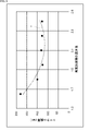
- FIG. 4 is a diagram showing the relationship between the refractive index of a high refractive index layer and the total film thickness at the time of optimal design;
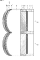
- FIG. 10 is a diagram showing an example of a cross-sectional structure of a main part of a pixel when the number of layers of the antireflection film is four.
- FIG. 4 is a diagram showing the relationship between the number of antireflection coating layers and reflectance.
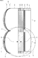
- FIG. 4 is a diagram showing the relationship between the center of a circle indicating the curvature of the surface of the on-chip microlens and the center of the circle indicating the curvature of the surface of the antireflection film.
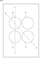
- FIG. 10 is a diagram showing a planar layout example when the on-chip microlenses are flat.
- FIG. 10 is a diagram showing an example of a cross-sectional structure of a main part of a pixel when the space between on-chip microlenses is flat;
- FIG. 10 is a diagram illustrating an example of a method for manufacturing a photodetector to which the present disclosure is applied;
- FIG. 10 is a diagram showing another example of a cross-sectional structure of a main part including pixels;
- FIG. 4 is a diagram showing the relationship between the number of antireflection coating layers and reflectance.
- FIG. 4 is a diagram showing the relationship between the number of antireflection coating layers and reflectance.
- FIG. 10 is a diagram showing another example of a method for manufacturing a photodetector to which the present disclosure is applied;
- FIG. 10 is a diagram showing another example of a method for manufacturing a photodetector to which the present disclosure is applied;
- 1 is a block diagram showing a configuration example of an electronic device equipped with a photodetector to which the present disclosure is applied;
- FIG. 1 is a block diagram showing an example of a schematic configuration of a vehicle control system;
- FIG. FIG. 4 is an explanatory diagram showing an example of installation positions of an outside information detection unit and an imaging unit;
- FIG. 1 is a diagram showing a configuration example of a photodetector to which the present disclosure is applied.
- a solid-state imaging device 10 is a CMOS (Complementary Metal Oxide Semiconductor) type solid-state imaging device, and is an example of a photodetector to which the present disclosure is applied.
- the solid-state imaging device 10 includes a pixel array section 21 , a vertical driving section 22 , a column signal processing section 23 , a horizontal driving section 24 , an output section 25 and a control section 26 .
- the pixel array section 21 has a plurality of pixels 100 two-dimensionally arranged in a matrix on a substrate made of silicon (Si).
- the pixel 100 has a photoelectric conversion unit made up of a photodiode and a plurality of pixel transistors.
- a pixel transistor is composed of a transfer transistor, a reset transistor, a selection transistor, and an amplification transistor.
- a pixel drive line 41 is formed for each row and connected to the vertical drive section 22, and a vertical signal line 42 is formed for each column. and connected to the column signal processing unit 23 .
- the vertical driving section 22 is configured by a shift register, an address decoder, etc., and drives each pixel 100 arranged in the pixel array section 21 . Pixel signals output from the pixels 100 selectively scanned by the vertical driving section 22 are supplied to the column signal processing section 23 through the vertical signal lines 42 .
- the column signal processing unit 23 performs predetermined signal processing on pixel signals output from each pixel 100 in the selected row through the vertical signal line 42 for each pixel column of the pixel array unit 21, and processes the pixel signals after the signal processing. Hold the signal temporarily. Specifically, the column signal processing unit 23 performs at least noise removal processing and correlated double sampling (CDS) processing as signal processing.
- CDS correlated double sampling
- the column signal processing unit 23 may be provided with, for example, an AD conversion (Analog/Digital Conversion) function to output the signal level as a digital signal.
- AD conversion Analog/Digital Conversion
- the horizontal driving section 24 is composed of a shift register, an address decoder, etc., and selects unit circuits corresponding to the pixel columns of the column signal processing section 23 in order. Pixel signals processed by the column signal processing unit 23 are output to the output unit 25 through the horizontal signal line 51 by selective scanning by the horizontal driving unit 24 .
- the output unit 25 performs predetermined signal processing on the pixel signals sequentially input from each of the column signal processing units 23 through the horizontal signal line 51, and outputs the resulting signal.
- the control unit 26 includes a timing generator or the like that generates various timing signals, and controls the vertical driving unit 22, the column signal processing unit 23, the horizontal driving unit 24, and the like based on the various timing signals generated by the timing generator. Drive control.
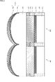
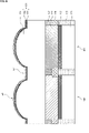
- FIG. 2 is a diagram showing an example of a cross-sectional structure of a main part including the pixel 100.
- FIG. FIG. 2 shows the cross-sectional structure of two adjacent pixels among the plurality of pixels 100 arranged in the pixel array section 21 .
- part of the photodiode and structures formed in layers below it are omitted.
- the pixel 100 has a photodiode 111 as a photoelectric conversion unit.
- the photodiode 111 is formed, for example, in a first-conductivity-type well region formed in a semiconductor substrate such as a silicon substrate, including first-conductivity-type and second-conductivity-type semiconductor regions.
- the first conductivity type is p-type and the second conductivity type is n-type.
- An insulating film 112 is formed on the upper surface of the photodiode 111 , and a color filter 113 and an on-chip microlens 114 corresponding to each pixel 100 are laminated on the flat surface of the insulating film 112 .
- color filters 113 for example, color filters corresponding to red (R), green (G), and blue (B) wavelengths can be used. Further, as the color filters 113 formed in the plurality of pixels 100 arranged two-dimensionally in the pixel array section 21, color filters corresponding to the Bayer arrangement can be used.
- the on-chip microlens 114 is formed of, for example, an organic film.
- an antireflection film 121 in which an inorganic film 131 and an inorganic film 132 are laminated is formed.
- the inorganic film 131 is made of a material having a higher refractive index than the on-chip microlens 114 .
- the inorganic film 132 is made of a material having a lower refractive index than the on-chip microlens 114 and the inorganic film 131 .
- the inorganic film 131 satisfies N1 ⁇ 1.8, where N1 is the refractive index, and a highly reliable metal oxide film is used as the film type.
- the film type of the inorganic film 131 may be a tantalum oxide film (Ta 2 O 5 film), a niobium oxide film (Nb 2 O 5 film), a titanium oxide film (TiO 2 film), or a hafnium oxide film (HfO 2 film). ) is used.
- the refractive index of the inorganic film 132 is N2 ⁇ 1.55.
- a silicon oxide film (SiO 2 film), a silicon oxycarbide film (SiOC film), or the like is used as the film type of the inorganic film 132.
- the inorganic film 131 can be said to be a high refractive index layer because it has a higher refractive index than the inorganic film 132.
- the inorganic film 132 can be said to be a low refractive index layer because it has a lower refractive index than the inorganic film 131. That is, in FIG. 2, the antireflection film 121 has a structure in which two layers, a high refractive index layer as the inorganic film 131 and a low refractive index layer as the inorganic film 132, are laminated.
- a light shielding film 116 and an insulating film 117 are laminated on the well region 115. As shown in FIG. 2,
- Patent Document 1 discloses a configuration using a silicon nitride film (SiN film) as a high refractive index layer in an antireflection film.
- SiN film silicon nitride film
- the inventor of the present disclosure found that, in a constant temperature and humidity test, when a silicon nitride film was used as the high refractive index layer in the antireflection film, the silicon nitride film was oxidized at the interface between the on-chip microlens and the silicon nitride film. , it has been confirmed that there is a possibility of affecting characteristics such as sensitivity characteristics.
- An inorganic film 131 formed of a metal oxide film such as an oxide film is used. That is, since the film type of the inorganic film 131 is a metal oxide film (such as a tantalum oxide film), which is originally oxidized and has the property that the film is dense, the refractive index does not readily fluctuate. The high refractive index layer in has high reliability.
- the antireflection film 121 is designed to be thinner (AR (Anti Reflection Film)).
- AR Anti Reflection Film
- a silicon nitride film has a refractive index of about 1.85
- a metal oxide film has a refractive index of about 2 to 2.5.
- FIG. 3 shows the refractive index of the high refractive index layer and the total film thickness, where the horizontal axis is the refractive index of the high refractive index layer and the vertical axis is the film thickness (total film thickness) of the antireflection film in the optimum design. is represented by a curve L.
- the refractive index of the high refractive index layer corresponds to the refractive index of the inorganic film 131 and the total film thickness corresponds to the film thickness of the antireflection film 121 .
- the silicon nitride film has a refractive index of about 1.85
- the metal oxide film forming the inorganic film 131 has a refractive index of about 2 to 2.5.
- AR can be designed to make the film thickness of the film thinner.
- a metal oxide film is used as the inorganic film 131 which is the high refractive index layer as a combination of the high refractive index layer and the low refractive index layer, and the silicon nitride film is used. Since the refractive index can be increased compared to the conventional case, even if AR design is performed with a thinner film, it is possible to achieve the same optical path length as when using a silicon nitride film, and thinning can be realized. can.
- the light collection efficiency varies greatly depending on the distance between the top position (center) of the on-chip microlens and the silicon substrate. thickness), the top position of the on-chip microlens is separated from the silicon substrate. As a result, the light collection efficiency decreases, which leads to a decrease in the quantum efficiency (QE), so it is necessary to reduce the thickness of the antireflection coating.
- QE quantum efficiency
- the film thickness of the inorganic film 131 as the high refractive index layer is made equal to or less than the film thickness of the inorganic film 132 as the low refractive index layer. That is, when the film thickness of the inorganic film 131 is T1 and the film thickness of the inorganic film 132 is T2, it is designed to have a relationship of T1 ⁇ T2.
- AR design is performed so that the film thickness (total film thickness) of the antireflection film 121 is 200 nm or less.
- the inventors of the present disclosure found that by using a metal oxide film instead of a silicon nitride film as the high refractive index layer in the antireflection film, it is possible to reduce the total film thickness by about 100 nm. , we have confirmed that AR design is possible with a total film thickness of 200 nm or less.
- a metal oxide film such as a tantalum oxide film is used as the high refractive index layer in the antireflection film 121 formed on the surface of the on-chip microlens 114. , it is possible to improve the reliability and to design the AR with a thinner film.
- the antireflection film 121 is composed of two layers in which a high refractive index layer and a low refractive index layer are laminated has been described. You may make it form from the number of layers, such as four layers laminated
- FIG. 4 is a diagram showing an example of the cross-sectional structure of the main part of the pixel 100 when the antireflection film 121 has four layers.
- parts corresponding to those in FIG. 2 are denoted by the same reference numerals, and description thereof will be omitted as appropriate.
- the antireflection film 121 is formed by laminating an inorganic film 141, an inorganic film 142, an inorganic film 143, and an inorganic film 144.
- the inorganic films 141 and 143 are high refractive index layers
- the inorganic films 142 and 144 are low refractive index layers
- the high refractive index layers and the low refractive index layers are alternately arranged.
- the inorganic film 141 and the inorganic film 143 are made of a metal oxide film such as a tantalum oxide film, a niobium oxide film, a titanium oxide film, or a hafnium oxide film. .
- the inorganic film 141 and the inorganic film 143 may be of the same film type, or may be of different film types.
- N1 is the refractive index of each of the inorganic film 141 and the inorganic film 143, N1 ⁇ 1.8.
- a silicon oxide film, a silicon oxycarbide film, or the like is used, like the inorganic film 132 (FIG. 2).
- the inorganic film 142 and the inorganic film 144 may be of the same film type, or may be of different film types.
- N2 is the refractive index of each of the inorganic film 142 and the inorganic film 144, N2 ⁇ 1.55.
- the antireflection film 121 high refractive index layers (inorganic films 141, 143) and low refractive index layers (inorganic films 142, 144) are alternately laminated.
- the low refractive index layers (inorganic films 142, 144) are formed on the surfaces of the high refractive index layers (inorganic films 141, 143).
- the low refractive index layer (inorganic film 144) is formed on the outermost surface.
- FIG. 5 shows the relationship between the number of layers of the antireflection film 121 and the reflectance by curves L1 to L4, where the horizontal axis is the wavelength and the vertical axis is the reflectance.
- the relationship when the number of layers is 1 is represented by curve L1
- the relationship when the number of layers is 2 is represented by curve L2
- the relationship when the number of layers is 3 is represented by curve L1.
- L3 and curve L4 represent the relationship when the number of layers is four.
- the reflectance can be further reduced by increasing the number of layers in the antireflection film 121, as indicated by curves L1 to L4. For example, when the number of layers of the antireflection film 121 is four, the reflectance is lower even in the same wavelength region as compared with the case where the number of layers is one to three.
- the antireflection film 121 formed on the surface of the on-chip microlens 114 is four layers in which high refractive index layers and low refractive index layers are alternately laminated.
- the surface reflection of the on-chip microlens 114 can be further suppressed, and image quality deterioration such as flare can be suppressed.
- the anti-reflection film 121 has a structure in which four high refractive index layers and low refractive index layers are alternately laminated. It does not matter if the number of layers is large. For example, when laminating 6 layers, the 5th layer is a high refractive index layer, the 6th layer is a low refractive index layer, and the 6th low refractive index layer is the outermost layer.
- the film thickness of the portion corresponding to the edge portion (bottom position) of the on-chip microlens 114 is greater than the film thickness of the portion corresponding to the center portion (top position) of the on-chip microlens 114 .
- the anti-reflection film 121 is made thinner from the portion corresponding to the center portion of the on-chip microlens 114 toward the portion corresponding to the edge portion.
- FIG. 6 is a diagram showing the relationship between the center of the circle indicating the curvature of the surface of the on-chip microlens 114 and the center of the circle indicating the curvature of the surface of the antireflection film 121 .
- parts corresponding to those in FIG. 2 are denoted by the same reference numerals, and description thereof will be omitted.
- a circle C1 indicating the curvature of the surface of the on-chip microlens 114 is indicated by a dashed line
- a circle C2 indicating the curvature of the surface of the antireflection film 121 is indicated by a chain double-dashed line. Also, the relationship between the center O1 of the circle C1 and the center O2 of the circle C2 is shown.
- the film thickness becomes the same at the part where the
- the film thickness of the antireflection film 121 is thin near the edge of the on-chip microlens 114. Therefore, in the solid-state imaging device 10 to which the present disclosure is applied, as shown in FIG. , the center O2 of the circle C2 representing the curvature of the surface of the antireflection film 121 is located on the light incident side (upper side in the drawing) than the center O1 of the circle C1 representing the curvature of the surface of the on-chip microlens 114. It's located in.
- the film thickness of the portion corresponding to the edge portion of the on-chip microlens 114 is smaller than the film thickness a of the portion corresponding to the center portion of the on-chip microlens 114 .
- the b becomes thinner (there is a relationship of a>b).
- the center O2 of the circle C2 is located on the light incident side (upper side in the figure) than the center O1 of the circle C1 ( The positions of the center O1 and the center O2 of the circle C2 do not match), and the antireflection film 121 formed on the surface of the on-chip microlens 114 is not formed conformally.
- the inorganic film 131 as a high refractive index layer and the inorganic film 132 as a low refractive index layer are laminated.
- the centers of the circles representing the respective surface curvatures of the inorganic film 131 and the inorganic film 132 are located on the light incident side of the center O1 of the circle C1. Therefore, in the antireflection film 121 formed on the surface of the on-chip microlens 114, the film thickness on the edge portion side is thinner than the film thickness on the central portion, and compared to the case where the film thickness is made uniform, Characteristics such as sensitivity characteristics can be improved.
- high refractive index layers inorganic films 141 and 143
- low refractive index layers inorganic films 142 and 144) are alternately laminated to form four layers. None of the inorganic films 141 to 144 are conformal, and the center of the circle indicating the surface curvature of each of the inorganic films 141 to 144 is preferably located on the light incident side of the center O1 of the circle C1.
- concave portions A1 (gap portions of the on-chip microlenses 114), which are V-shaped recessed regions, are formed. .
- the antireflection film 121 is also formed in the concave portion A1, and the antireflection film 121 is not cut off between the on-chip microlenses 114.
- the area between the on-chip microlenses 114 is not limited to the V-shaped recessed area, and may be a flat area.
- the space between the on-chip microlenses 114 becomes a flat area.
- FIG. 8 shows the X1-X1' section of the planar layout of FIG.
- parts corresponding to those in FIG. 2 are denoted by the same reference numerals, and description thereof will be omitted as appropriate.
- the film thickness of the antireflection film 121 corresponds to the flat portion A2.
- the portion corresponding to the central portion A3 is substantially the same as the portion corresponding to the central portion A3.
- the thickness of the film 121 is substantially the same between the portion corresponding to the flat portion A2 between the on-chip microlenses 114 and the portion corresponding to the central portion A3 of the on-chip microlens 114, and similar effects can be obtained. .
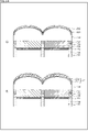
- FIG. 9 is a diagram illustrating an example of a method for manufacturing a photodetector to which the present disclosure is applied.
- FIG. 9 shows the process after forming the on-chip microlens 114 . That is, although not shown, an imaging region is formed on a silicon substrate in which photodiodes 111 and the like are formed and a plurality of pixels 100 are arranged two-dimensionally. An insulating film 112 is formed on the upper surface of the photodiode 111 to planarize the surface, and a color filter 113 corresponding to red, green, or blue wavelengths is formed thereon.
- on-chip microlenses 114 are formed on the color filters 113 .
- an inorganic film 131 is formed on the surface of the on-chip microlens 114 .
- the inorganic film 131 is formed using a chemical vapor deposition (CVD) method, a physical vapor deposition (PVD) method, an atomic layer deposition (ALD) method, or the like. be able to.
- CVD chemical vapor deposition
- PVD physical vapor deposition
- ALD atomic layer deposition
- a metal oxide film such as a tantalum oxide film, a niobium oxide film, a titanium oxide film, or a hafnium oxide film is formed.
- an inorganic film 132 is formed on the surface of the inorganic film 131. Then, as shown in FIG. 9C, an inorganic film 132 is formed on the surface of the inorganic film 131. Then, as shown in FIG.
- the inorganic film 132 can be deposited using a chemical vapor deposition method, a physical vapor deposition method, an atomic layer deposition method, or the like.
- a silicon oxide film, a silicon oxycarbide film, or the like is formed.
- the antireflection film 121 formed by laminating the inorganic film 131 and the inorganic film 132 is not conformal, and the center of the circle indicating the curvature of each surface of the inorganic film 131 and the inorganic film 132 is the surface of the on-chip microlens 114.
- the film is formed so as to be located on the light incident side (upper side in the figure) from the center of the circle showing the curvature of .
- an antireflection film 121 (FIG. 2) consisting of two layers of inorganic films 131 and 132 (two layers of a high refractive index layer and a low refractive index layer) is formed on the surface of the on-chip microlens 114 .
- a formed solid-state imaging device 10 is obtained.
- FIG. 9 shows a manufacturing method in which the antireflection film 121 has two layers
- a similar manufacturing method can be used when the antireflection film 121 has four layers. That is, by repeating the steps shown in FIGS. 9B and 9C, inorganic films 141, 142, and 143 are formed by chemical vapor deposition, physical vapor deposition, atomic layer deposition, or the like. , and an inorganic film 144 are sequentially deposited, and an on-chip microlens 114 is formed with an antireflection film 121 (FIG. 4) consisting of four layers in which high refractive index layers and low refractive index layers are alternately laminated. An imaging device 10 is obtained.
- the solid-state imaging device 10 to which the present disclosure is applied adopts the configuration of the antireflection film as shown in FIG. To suppress deterioration of image quality such as flare while maintaining high reliability by improving adhesion between a lens and an on-chip microlens.
- FIG. 10 is a diagram showing another example of the cross-sectional structure of the essential part including the pixel 100. As shown in FIG. In FIG. 10, parts corresponding to those in FIG. 2 are denoted by the same reference numerals, and description thereof will be omitted as appropriate.
- the cross-sectional structure of FIG. 10 has an antireflection film 221 instead of the antireflection film 121 formed on the surface of the on-chip microlens 114 .
- the antireflection film 221 is formed by laminating an inorganic film 231 and an inorganic film 232 .
- the inorganic film 231 is made of a material having a higher refractive index than the on-chip microlens 114 .
- the inorganic film 232 is made of a material having a lower refractive index than the on-chip microlens 114 and the inorganic film 231 .
- the inorganic film 231 is an adhesion film (adhesion layer) for improving adhesion between the on-chip microlens 114 and the inorganic film 232 .
- the refractive index of the inorganic film 231 is N3 ⁇ 1.55, for example.
- an LTO (Low Temperature Oxidation) film such as a silicon oxide film (SiO 2 film) is used.
- the inorganic film 232 is a structural film having a moth-eye structure in which fine irregularities are formed. Since the inorganic film 232 has fine irregularities, it is possible to reduce the reflection of light in the working wavelength range.
- the refractive index of the inorganic film 232 is N4, for example, N4 ⁇ 1.4.
- the refractive index of the AlOx film is assumed to be about 1.6, but the air layer is formed in the recessed portions due to the fine irregularities, so the total refractive index is reduced to about 1.3.
- the film thickness of the inorganic film 232 can be, for example, about 270 nm between top and bottom.
- the top position is the highest position of the projections in the fine uneven shape
- the bottom position is the position of the interface with the inorganic film 231 .
- the inorganic film 232 is a structural film having fine irregularities, but the inorganic film 231 as the adhesion film is not exposed, and the inorganic film 232 is the outermost surface.
- the inorganic film 231 can be said to be a low refractive index layer because it has a refractive index similar to that of the inorganic film 132.
- the inorganic film 232 has a lower refractive index than the inorganic film 231, so it can be said that it is an ultra-low refractive index layer having a lower refractive index than the low refractive index layer.
- the antireflection film 121 is formed by alternately stacking high refractive index layers and low refractive index layers. Other layers may be laminated as long as the low second layer is laminated.
- an ultra-low refractive index layer which is the inorganic film 232
- the inorganic film 232 can also be said to be a structural film formed by processing the surface of a film to be processed having a predetermined refractive index (for example, an AlOx film having a refractive index of 1.6) to have a fine uneven shape. .
- curves L22 to L29 represent.
- the film thickness of the inorganic film 231 can be the film thickness of the portion corresponding to the central portion (top position) of the on-chip microlens 114 .
- a curve L20 represents the reflectance in the wavelength region when the inorganic film 231 as the antireflection film 221 is composed of a single film.
- a curve L21 represents the reflectance in the wavelength region assuming that the inorganic film 232 is composed of a single film.
- the reflectances of curves L26 to L29 are lowered as a whole and do not exceed the reflectance of curve L21.
- the film thickness of the inorganic film 231 is further increased to 200 nm, 300 nm, 500 nm, and 1000 nm, the reflectance becomes low in the wavelength region of 400 to 700 nm, and the inorganic film 231 is not laminated. It shows that the reflectance is not deteriorated as compared with the case (when the inorganic film 232 is a single film).
- the inventors of the present disclosure have found that when the thickness of the inorganic film 231 is set to 500 nm and 1000 nm, although the reflectance does not deteriorate, interference occurs due to the thickness of the inorganic film 231. Therefore, it is not practical. Therefore, it has been confirmed that the film thickness of the inorganic film 231 is preferably 10 nm or more and 300 nm or less.
- the film thickness of the inorganic film 231 as an adhesion film between the on-chip microlens 114 and the inorganic film 232 is set to 10 to 300 nm. Therefore, it is possible to suppress deterioration of image quality such as flare while improving adhesion and maintaining high reliability.
- an LTO film such as a silicon oxide film is used for the inorganic film 231, and there is no problem in adhesion with the on-chip microlens 114, and there is no problem in adhesion with the inorganic film 232. , the adhesion between the on-chip microlens 114 and the inorganic film 232 can be improved. As a result, the inorganic film 231 does not peel off from the on-chip microlens 114, and as a result, peeling of the inorganic film 232 on the outermost surface can be suppressed.
- an inorganic film 231 and an inorganic film 232 are laminated, and the inorganic film 232 is a structural film having fine irregularities for reducing reflection of light.
- the inorganic film 232 is a structural film having fine irregularities for reducing reflection of light.
- the reflectance is lower than when the inorganic film 232 is composed of a single film. can. As a result, deterioration of image quality such as flare can be suppressed more reliably.
- an antireflection film 221 on the surface of the on-chip microlens 114, damage to the on-chip microlens 114 can be suppressed. Note that the antireflection film 221 can be formed on the surface of the on-chip microlens 114 even when the pixel 100 is a fine pixel.
- Example of manufacturing method 13 and 14 are diagrams showing another example of a method for manufacturing a photodetector to which the present disclosure is applied.
- FIG. 13 shows the steps after forming the on-chip microlenses 114, as in FIG. That is, an imaging region is formed in which a plurality of pixels 100 are arranged two-dimensionally by forming photodiodes 111 and the like on a silicon substrate. An insulating film 112 is formed on the upper surface of the photodiode 111 to planarize the surface, and a color filter 113 corresponding to red, green, or blue wavelengths is formed thereon.
- on-chip microlenses 114 are formed on the color filters 113 .
- an inorganic film 231 is formed on the surface of the on-chip microlens 114 .
- the inorganic film 231 can be deposited using a chemical vapor deposition (CVD) method, a physical vapor deposition (PVD) method, an atomic layer deposition (ALD) method, or the like.
- CVD chemical vapor deposition
- PVD physical vapor deposition
- ALD atomic layer deposition
- LTO film such as a silicon oxide film is formed.
- an inorganic film 232 is formed on the surface of the inorganic film 231 .
- the inorganic film 232 can be deposited using an atomic layer deposition (ALD) method or the like.
- ALD atomic layer deposition
- As the inorganic film 232 for example, an AlOx film is formed.
- the inorganic film 231 serves as an adhesion film (adhesion layer) that bonds the on-chip microlens 114 and the inorganic film 232 together.
- the inorganic film 232 has a fine uneven shape as shown in E of FIG. A structural film is formed. That is, the inorganic film 232 is formed of an AlOx film or the like. In this manner, an antireflection film 221 composed of two layers (a low refractive index layer and an ultra-low refractive index layer) of the inorganic film 231 and the inorganic film 232 was formed on the surface of the on-chip microlens 114. A solid-state imaging device 10 is obtained.
- DIW pure water
- CMOS-type solid-state imaging device was described as the solid-state imaging device 10, but the CMOS-type solid-state imaging device is formed in a lower layer when viewed from the silicon substrate on which the photodiodes 111 as photoelectric conversion units are formed.
- a back-illuminated structure can be employed in which light is incident from the upper layer (back side) on the opposite side of the wiring layer side (front side).
- the CMOS solid-state imaging device may have a surface illumination type structure in which the light incident side is the wiring layer side (surface side).
- the solid-state imaging device 10 is an example of a photodetector to which the present disclosure is applied. That is, the photodetector to which the present disclosure is applied can be applied not only to the solid-state imaging device 10 but also to a device that detects light, such as a ranging sensor using an IR laser. Note that the configuration of the antireflection film to which the present disclosure is applied is not limited to CMOS solid-state imaging devices, and can also be applied to CCD (Charge Coupled Device) solid-state imaging devices.
- CCD Charge Coupled Device
- the solid-state imaging device 10 is configured such that the first conductivity type is p-type and the second conductivity type is n-type. I don't mind. Further, in the above description, the solid-state imaging device 10 has a configuration in which primary color filters corresponding to the wavelengths of red (R), green (G), and blue (B) are used as the color filters 113. Complementary color filters corresponding to the wavelengths of cyan (C), magenta (M), and yellow (Y) may be used.
- FIG. 15 is a block diagram showing a configuration example of an electronic device equipped with a photodetector to which the present disclosure is applied.
- an electronic device 1000 includes an optical system 1011 including a lens group, a photodetector 1012 having a function corresponding to the solid-state imaging device 10 in FIG. It has an imaging system consisting of In the electronic device 1000, in addition to the imaging system, a CPU (Central Processing Unit) 1010, a frame memory 1014, a display 1015, an operation system 1016, an auxiliary memory 1017, a communication I/F 1018, and a power supply system 1019 are connected via a bus 1020. It becomes the composition connected mutually.
- a CPU Central Processing Unit
- a CPU 1010 controls the operation of each part of the electronic device 1000 .
- the optical system 1011 takes in incident light (image light) from a subject and forms an image on the photodetection surface of the photodetection element 1012 .
- the photodetector 1012 converts the amount of incident light imaged on the photodetection surface by the optical system 1011 into an electric signal for each pixel and outputs the electric signal as a pixel signal.
- the DSP 1013 performs predetermined signal processing on the signal output from the photodetector 1012 .
- the frame memory 1014 temporarily records image data of still images or moving images captured by the imaging system.
- a display 1015 is a liquid crystal display or an organic EL display, and displays still images or moving images captured by the imaging system.
- the operation system 1016 issues operation commands for various functions of the electronic device 1000 according to user's operations.
- the auxiliary memory 1017 is a storage medium including semiconductor memory such as flash memory, and records image data of still images or moving images captured by the imaging system.
- the communication I/F 1018 has a communication module compatible with a predetermined communication method, and transmits image data of still images or moving images captured by the imaging system to other devices via a network.
- the power supply system 1019 appropriately supplies various types of power as operating power to the CPU 1010, DSP 1013, frame memory 1014, display 1015, operation system 1016, auxiliary memory 1017, and communication I/F 1018.
- the technology (this technology) according to the present disclosure can be applied to various products.
- the technology according to the present disclosure can be realized as a device mounted on any type of moving body such as automobiles, electric vehicles, hybrid electric vehicles, motorcycles, bicycles, personal mobility, airplanes, drones, ships, and robots. may
- FIG. 16 is a block diagram showing a schematic configuration example of a vehicle control system, which is an example of a mobile control system to which the technology according to the present disclosure can be applied.
- a vehicle control system 12000 includes a plurality of electronic control units connected via a communication network 12001.
- the vehicle control system 12000 includes a drive system control unit 12010, a body system control unit 12020, an exterior information detection unit 12030, an interior information detection unit 12040, and an integrated control unit 12050.
- a microcomputer 12051, an audio/image output unit 12052, and an in-vehicle network I/F (interface) 12053 are illustrated.
- the drive system control unit 12010 controls the operation of devices related to the drive system of the vehicle according to various programs.
- the driving system control unit 12010 includes a driving force generator for generating driving force of the vehicle such as an internal combustion engine or a driving motor, a driving force transmission mechanism for transmitting the driving force to the wheels, and a steering angle of the vehicle. It functions as a control device such as a steering mechanism to adjust and a brake device to generate braking force of the vehicle.
- the body system control unit 12020 controls the operation of various devices equipped on the vehicle body according to various programs.
- the body system control unit 12020 functions as a keyless entry system, a smart key system, a power window device, or a control device for various lamps such as headlamps, back lamps, brake lamps, winkers or fog lamps.
- the body system control unit 12020 can receive radio waves transmitted from a portable device that substitutes for a key or signals from various switches.
- the body system control unit 12020 receives the input of these radio waves or signals and controls the door lock device, power window device, lamps, etc. of the vehicle.
- the vehicle exterior information detection unit 12030 detects information outside the vehicle in which the vehicle control system 12000 is installed.
- the vehicle exterior information detection unit 12030 is connected with an imaging section 12031 .
- the vehicle exterior information detection unit 12030 causes the imaging unit 12031 to capture an image of the exterior of the vehicle, and receives the captured image.
- the vehicle exterior information detection unit 12030 may perform object detection processing or distance detection processing such as people, vehicles, obstacles, signs, or characters on the road surface based on the received image.
- the imaging unit 12031 is an optical sensor that receives light and outputs an electrical signal according to the amount of received light.
- the imaging unit 12031 can output the electric signal as an image, and can also output it as distance measurement information.
- the light received by the imaging unit 12031 may be visible light or non-visible light such as infrared rays.
- the in-vehicle information detection unit 12040 detects in-vehicle information.
- the in-vehicle information detection unit 12040 is connected to, for example, a driver state detection section 12041 that detects the state of the driver.
- the driver state detection unit 12041 includes, for example, a camera that captures an image of the driver, and the in-vehicle information detection unit 12040 detects the degree of fatigue or concentration of the driver based on the detection information input from the driver state detection unit 12041. It may be calculated, or it may be determined whether the driver is dozing off.
- the microcomputer 12051 calculates control target values for the driving force generator, the steering mechanism, or the braking device based on the information inside and outside the vehicle acquired by the vehicle exterior information detection unit 12030 or the vehicle interior information detection unit 12040, and controls the drive system control unit.
- a control command can be output to 12010 .
- the microcomputer 12051 realizes the functions of ADAS (Advanced Driver Assistance System) including collision avoidance or shock mitigation of vehicles, follow-up driving based on inter-vehicle distance, vehicle speed maintenance driving, vehicle collision warning, vehicle lane deviation warning, etc. Cooperative control can be performed for the purpose of ADAS (Advanced Driver Assistance System) including collision avoidance or shock mitigation of vehicles, follow-up driving based on inter-vehicle distance, vehicle speed maintenance driving, vehicle collision warning, vehicle lane deviation warning, etc. Cooperative control can be performed for the purpose of ADAS (Advanced Driver Assistance System) including collision avoidance or shock mitigation of vehicles, follow-up driving based on inter-vehicle distance, vehicle speed maintenance driving
- the microcomputer 12051 controls the driving force generator, the steering mechanism, the braking device, etc. based on the information about the vehicle surroundings acquired by the vehicle exterior information detection unit 12030 or the vehicle interior information detection unit 12040, so that the driver's Cooperative control can be performed for the purpose of autonomous driving, etc., in which vehicles autonomously travel without depending on operation.
- the microcomputer 12051 can output a control command to the body system control unit 12020 based on the information outside the vehicle acquired by the information detection unit 12030 outside the vehicle.
- the microcomputer 12051 controls the headlamps according to the position of the preceding vehicle or the oncoming vehicle detected by the vehicle exterior information detection unit 12030, and performs cooperative control aimed at anti-glare such as switching from high beam to low beam. It can be carried out.
- the audio/image output unit 12052 transmits at least one of audio and/or image output signals to an output device capable of visually or audibly notifying the passengers of the vehicle or the outside of the vehicle.
- an audio speaker 12061, a display unit 12062, and an instrument panel 12063 are illustrated as output devices.
- the display unit 12062 may include at least one of an on-board display and a head-up display, for example.
- FIG. 17 is a diagram showing an example of the installation position of the imaging unit 12031.
- the vehicle 12100 has imaging units 12101, 12102, 12103, 12104, and 12105 as the imaging unit 12031.
- the imaging units 12101, 12102, 12103, 12104, and 12105 are provided at positions such as the front nose of the vehicle 12100, the side mirrors, the rear bumper, the back door, and the upper part of the windshield in the vehicle interior, for example.
- An image pickup unit 12101 provided in the front nose and an image pickup unit 12105 provided above the windshield in the passenger compartment mainly acquire images in front of the vehicle 12100 .
- Imaging units 12102 and 12103 provided in the side mirrors mainly acquire side images of the vehicle 12100 .
- An imaging unit 12104 provided in the rear bumper or back door mainly acquires an image behind the vehicle 12100 .
- Forward images acquired by the imaging units 12101 and 12105 are mainly used for detecting preceding vehicles, pedestrians, obstacles, traffic lights, traffic signs, lanes, and the like.
- FIG. 17 shows an example of the imaging range of the imaging units 12101 to 12104.
- the imaging range 12111 indicates the imaging range of the imaging unit 12101 provided in the front nose
- the imaging ranges 12112 and 12113 indicate the imaging ranges of the imaging units 12102 and 12103 provided in the side mirrors, respectively
- the imaging range 12114 The imaging range of an imaging unit 12104 provided on the rear bumper or back door is shown. For example, by superimposing the image data captured by the imaging units 12101 to 12104, a bird's-eye view image of the vehicle 12100 viewed from above can be obtained.
- At least one of the imaging units 12101 to 12104 may have a function of acquiring distance information.
- at least one of the imaging units 12101 to 12104 may be a stereo camera composed of a plurality of imaging elements, or may be an imaging element having pixels for phase difference detection.
- the microcomputer 12051 determines the distance to each three-dimensional object within the imaging ranges 12111 to 12114 and changes in this distance over time (relative velocity with respect to the vehicle 12100). , it is possible to extract, as the preceding vehicle, the closest three-dimensional object on the course of the vehicle 12100, which runs at a predetermined speed (for example, 0 km/h or more) in substantially the same direction as the vehicle 12100. can. Furthermore, the microcomputer 12051 can set the inter-vehicle distance to be secured in advance in front of the preceding vehicle, and perform automatic brake control (including following stop control) and automatic acceleration control (including following start control). In this way, cooperative control can be performed for the purpose of automatic driving in which the vehicle runs autonomously without relying on the operation of the driver.
- automatic brake control including following stop control
- automatic acceleration control including following start control
- the microcomputer 12051 converts three-dimensional object data related to three-dimensional objects to other three-dimensional objects such as motorcycles, ordinary vehicles, large vehicles, pedestrians, and utility poles. It can be classified and extracted and used for automatic avoidance of obstacles. For example, the microcomputer 12051 distinguishes obstacles around the vehicle 12100 into those that are visible to the driver of the vehicle 12100 and those that are difficult to see. Then, the microcomputer 12051 judges the collision risk indicating the degree of danger of collision with each obstacle, and when the collision risk is equal to or higher than the set value and there is a possibility of collision, an audio speaker 12061 and a display unit 12062 are displayed. By outputting an alarm to the driver via the drive system control unit 12010 and performing forced deceleration and avoidance steering via the drive system control unit 12010, driving support for collision avoidance can be performed.
- At least one of the imaging units 12101 to 12104 may be an infrared camera that detects infrared rays.
- the microcomputer 12051 can recognize a pedestrian by determining whether or not the pedestrian exists in the captured images of the imaging units 12101 to 12104 .
- recognition of a pedestrian is performed by, for example, a procedure for extracting feature points in images captured by the imaging units 12101 to 12104 as infrared cameras, and performing pattern matching processing on a series of feature points indicating the outline of an object to determine whether or not the pedestrian is a pedestrian.
- the audio image output unit 12052 outputs a rectangular outline for emphasis to the recognized pedestrian. is superimposed on the display unit 12062 . Also, the audio/image output unit 12052 may control the display unit 12062 to display an icon or the like indicating a pedestrian at a desired position.
- the technology according to the present disclosure can be applied to the imaging unit 12031 among the configurations described above.
- the solid-state imaging device 10 in FIG. 1 can be applied to the imaging unit 12031 .
- image quality deterioration such as flare can be suppressed, and a more viewable captured image can be obtained, so it is possible to reduce driver fatigue.
- the present disclosure can be configured as follows.
- the antireflection film is a first inorganic film formed of a metal oxide film; and a second inorganic film formed on the surface of the first inorganic film and having a refractive index lower than that of the first inorganic film.
- the first inorganic film is a tantalum oxide film, a niobium oxide film, a titanium oxide film, or a hafnium oxide film.
- the first inorganic film has a refractive index of 1.8 or more, The photodetector according to any one of (1) to (3), wherein the second inorganic film has a refractive index of 1.55 or less.
- the first inorganic film is formed on the surface of the on-chip microlens, The photodetector according to any one of (1) to (6), wherein the second inorganic film is formed on the outermost surface. (8) The photodetector according to any one of (1) to (7), wherein the first inorganic film and the second inorganic film are alternately laminated. (9) The first inorganic film is an adhesive film formed on the surface of the on-chip microlens and bonding the on-chip microlens and the second inorganic film, The photodetector according to (1), wherein the second inorganic film is formed on the outermost surface and is a structural film having fine irregularities.
- the first inorganic film is an LTO film, The photodetector according to (9), wherein the second inorganic film is formed of an AlOx film.
- the film thickness of the portion corresponding to the edge portion of the on-chip microlens is thinner than the film thickness of the portion corresponding to the center portion of the on-chip microlens. 8) The photodetector according to any one of the above.
- the antireflection film is a first inorganic film;
- a second inorganic film which is a structural film formed on the surface of the first inorganic film and having a predetermined refractive index, is formed by processing the surface of the film to be processed to have a fine uneven shape.
- a photodetector comprising: (20) The first inorganic film is an adhesive film formed on the surface of the on-chip microlens and bonding the on-chip microlens and the second inorganic film, The photodetector according to (19), wherein the second inorganic film is a structural film formed on the outermost surface. (21) The first inorganic film is an LTO film, The photodetector according to (19) or (20), wherein the film to be processed is an AlOx film. (22) The photodetector according to any one of (19) to (21), wherein the thickness of the first inorganic film is 10 nm or more and 300 nm or less.
- the antireflection film is a first inorganic film formed of a metal oxide film; and a second inorganic film formed on the surface of the first inorganic film and having a refractive index lower than that of the first inorganic film.
- 10 solid-state imaging device 21 pixel array section, 22 vertical drive section, 23 column signal processing section, 24 horizontal drive section, 25 output section, 26 control section, 100 pixels, 111 photodiode, 114 on-chip microlens, 121 antireflection Film, 131 Inorganic film, 132 Inorganic film, 141 Inorganic film, 142 Inorganic film, 143 Inorganic film, 144 Inorganic film, 221 Antireflection film, 231 Inorganic film, 232 Inorganic film, 1000 Electronic device, 1012 Photodetector
Landscapes
- Solid State Image Pick-Up Elements (AREA)
- Transforming Light Signals Into Electric Signals (AREA)
Abstract
Description
図1は、本開示を適用した光検出装置の構成例を示す図である。
次に、固体撮像装置10において、画素アレイ部21に2次元状に配列される画素100の構成を説明する。
上述した特許文献1において、反射防止膜における高屈折率層として、シリコン窒化膜(SiN膜)を用いた構成が開示されているのは、先に述べた通りである。本開示の発明者は、恒温恒湿試験で、反射防止膜における高屈折率層にシリコン窒化膜を用いた場合に、オンチップマイクロレンズとシリコン窒化膜との界面にてシリコン窒化膜が酸化され、感度特性等の特性に影響を及ぼす可能性があることを確認している。
上述した説明では、反射防止膜121として、高屈折率層と低屈折率層とを積層した2層からなる場合を説明したが、2層に限らず、例えば、高屈折率層と低屈折率層とを交互に積層した4層などの層数から形成されるようにしてもよい。
反射防止膜121のカバレッジ性に関しては、高屈折率層及び低屈折率層のいずれもコンフォーマルではないことが望ましい。例えば、反射防止膜121では、オンチップマイクロレンズ114の中心部(トップ位置)に対応した部分の膜厚よりも、オンチップマイクロレンズ114の縁端部(ボトム位置)に対応した部分の膜厚のほうが薄くなるようにする。また、反射防止膜121では、オンチップマイクロレンズ114の中心部に対応した部分から縁端部に対応した部分に向かうほど膜厚が薄くなるようにする。
図9は、本開示を適用した光検出装置の製造方法の例を示す図である。
図10は、画素100を含む要部の断面構造の他の例を示す図である。図10においては、図2と対応する部分には同一の符号を付しており、その説明は適宜省略する。
図11と図12は、横軸を波長とし、縦軸を反射率としたときに、反射防止膜221における無機膜231の膜厚と波長領域での反射率との関係を曲線L22乃至L29で表している。無機膜231の膜厚は、オンチップマイクロレンズ114の中心部(トップ位置)に対応した部分の膜厚とすることができる。図11と図12では、比較のために、反射防止膜221として無機膜231が単膜で構成される場合を想定したときの波長領域での反射率を曲線L20で表し、反射防止膜221として無機膜232が単膜で構成される場合を想定したときの波長領域での反射率を曲線L21で表している。
図13と図14は、本開示を適用した光検出装置の製造方法の他の例を示す図である。
上述した説明では、固体撮像装置10として、CMOS型の固体撮像装置を説明したが、CMOS型の固体撮像装置は、光電変換部としてのフォトダイオード111が形成されたシリコン基板から見て下層に形成される配線層側(表面側)とは反対側の上層(裏面側)から光を入射させる裏面照射型構造とすることができる。なお、CMOS型の固体撮像装置は、光を入射する側を配線層側(表面側)とした表面照射型構造としても構わない。
本開示を適用した光検出装置は、スマートフォン、タブレット型端末、携帯電話機、デジタルスチルカメラ、デジタルビデオカメラなどの電子機器に搭載することができる。図15は、本開示を適用した光検出装置を搭載した電子機器の構成例を示すブロック図である。
光電変換部を有する複数の画素と、
各画素に対応して形成されたオンチップマイクロレンズと、
前記オンチップマイクロレンズの表面上に形成された反射防止膜と
を有し、
前記反射防止膜は、
金属酸化膜で形成される第1の無機膜と、
前記第1の無機膜の表面上に形成され、前記第1の無機膜よりも屈折率が低い第2の無機膜と
を積層して構成される
光検出装置。
(2)
前記第1の無機膜は、タンタル酸化膜、ニオブ酸化膜、チタン酸化膜、又はハフニウム酸化膜である
前記(1)に記載の光検出装置。
(3)
前記第2の無機膜は、シリコン酸化膜、又はシリコン酸化炭化膜である
前記(1)又は(2)に記載の光検出装置。
(4)
前記第1の無機膜の屈折率は、1.8以上であり、
前記第2の無機膜の屈折率は、1.55以下である
前記(1)乃至(3)のいずれかに記載の光検出装置。
(5)
前記第1の無機膜の膜厚は、前記第2の無機膜の膜厚以下の厚みである
前記(1)乃至(4)のいずれかに記載の光検出装置。
(6)
前記反射防止膜の膜厚は、200nm以下である
前記(5)に記載の光検出装置。
(7)
前記第1の無機膜は、前記オンチップマイクロレンズの表面上に形成され、
前記第2の無機膜は、最表面に形成される
前記(1)乃至(6)のいずれかに記載の光検出装置。
(8)
前記第1の無機膜と前記第2の無機膜とが交互に積層される
前記(1)乃至(7)のいずれかに記載の光検出装置。
(9)
前記第1の無機膜は、前記オンチップマイクロレンズの表面上に形成され、前記オンチップマイクロレンズと前記第2の無機膜とを密着させる密着膜であり、
前記第2の無機膜は、最表面に形成され、微細な凹凸形状を有する構造膜である
前記(1)に記載の光検出装置。
(10)
前記第1の無機膜は、LTO膜であり、
前記第2の無機膜は、AlOx膜により形成される
前記(9)に記載の光検出装置。
(11)
前記第1の無機膜の膜厚は、10nm以上、かつ、300nm以下である
前記(9)又は(10)に記載の光検出装置。
(12)
前記反射防止膜は、前記オンチップマイクロレンズの中心部に対応した部分の膜厚よりも、前記オンチップマイクロレンズの縁端部に対応した部分の膜厚のほうが薄くなる
前記(1)乃至(8)のいずれかに記載の光検出装置。
(13)
前記反射防止膜は、前記オンチップマイクロレンズの中心部に対応した部分から縁端部に対応した部分に向かうほど膜厚が薄くなる
前記(12)に記載の光検出装置。
(14)
前記オンチップマイクロレンズの表面の曲率を示す円の第1の中心と、前記反射防止膜の表面の曲率を示す円の第2の中心との位置が不一致となる
前記(12)又は(13)のいずれかに記載の光検出装置。
(15)
前記第2の中心は、前記第1の中心よりも、光が入射する側に位置する
前記(14)に記載の光検出装置。
(16)
前記第2の中心は、前記第1の無機膜と前記第2の無機膜のそれぞれの表面の曲率を示す円の中心を含む
前記(14)又は(15)に記載の光検出装置。
(17)
前記オンチップマイクロレンズの間に、前記反射防止膜が形成される
前記(1)乃至(8)、(12)乃至(16)のいずれかに記載の光検出装置。
(18)
前記オンチップマイクロレンズの間には、平坦部が形成され、
前記反射防止膜の膜厚は、前記平坦部に対応した部分と、前記オンチップマイクロレンズの中心部に対応した部分とで、略同一とされる
前記(17)に記載の光検出装置。
(19)
光電変換部を有する複数の画素と、
各画素に対応して形成されたオンチップマイクロレンズと、
前記オンチップマイクロレンズの表面上に形成された反射防止膜と
を有し、
前記反射防止膜は、
第1の無機膜と、
前記第1の無機膜の表面上に形成され、所定の屈折率を有する被加工膜の表面に微細な凹凸形状を加工することで形成された構造膜である第2の無機膜と
を積層して構成される
光検出装置。
(20)
前記第1の無機膜は、前記オンチップマイクロレンズの表面上に形成され、前記オンチップマイクロレンズと前記第2の無機膜とを密着させる密着膜であり、
前記第2の無機膜は、最表面に形成される構造膜である
前記(19)に記載の光検出装置。
(21)
前記第1の無機膜は、LTO膜であり、
前記被加工膜は、AlOx膜である
前記(19)又は(20)に記載の光検出装置。
(22)
前記第1の無機膜の膜厚は、10nm以上、かつ、300nm以下である
前記(19)乃至(21)のいずれかに記載の光検出装置。
(23)
光電変換部を有する複数の画素と、
各画素に対応して形成されたオンチップマイクロレンズと、
前記オンチップマイクロレンズの表面上に形成された反射防止膜と
を有し、
前記反射防止膜は、
金属酸化膜で形成される第1の無機膜と、
前記第1の無機膜の表面上に形成され、前記第1の無機膜よりも屈折率が低い第2の無機膜と
を積層して構成される光検出装置を搭載した電子機器。
Claims (23)
- 光電変換部を有する複数の画素と、
各画素に対応して形成されたオンチップマイクロレンズと、
前記オンチップマイクロレンズの表面上に形成された反射防止膜と
を有し、
前記反射防止膜は、
金属酸化膜で形成される第1の無機膜と、
前記第1の無機膜の表面上に形成され、前記第1の無機膜よりも屈折率が低い第2の無機膜と
を積層して構成される
光検出装置。 - 前記第1の無機膜は、タンタル酸化膜、ニオブ酸化膜、チタン酸化膜、又はハフニウム酸化膜である
請求項1に記載の光検出装置。 - 前記第2の無機膜は、シリコン酸化膜、又はシリコン酸化炭化膜である
請求項2に記載の光検出装置。 - 前記第1の無機膜の屈折率は、1.8以上であり、
前記第2の無機膜の屈折率は、1.55以下である
請求項1に記載の光検出装置。 - 前記第1の無機膜の膜厚は、前記第2の無機膜の膜厚以下の厚みである
請求項1に記載の光検出装置。 - 前記反射防止膜の膜厚は、200nm以下である
請求項5に記載の光検出装置。 - 前記第1の無機膜は、前記オンチップマイクロレンズの表面上に形成され、
前記第2の無機膜は、最表面に形成される
請求項1に記載の光検出装置。 - 前記第1の無機膜と前記第2の無機膜とが交互に積層される
請求項7に記載の光検出装置。 - 前記第1の無機膜は、前記オンチップマイクロレンズの表面上に形成され、前記オンチップマイクロレンズと前記第2の無機膜とを密着させる密着膜であり、
前記第2の無機膜は、最表面に形成され、微細な凹凸形状を有する構造膜である
請求項1に記載の光検出装置。 - 前記第1の無機膜は、LTO膜であり、
前記第2の無機膜は、AlOx膜により形成される
請求項9に記載の光検出装置。 - 前記第1の無機膜の膜厚は、10nm以上、かつ、300nm以下である
請求項9に記載の光検出装置。 - 前記反射防止膜は、前記オンチップマイクロレンズの中心部に対応した部分の膜厚よりも、前記オンチップマイクロレンズの縁端部に対応した部分の膜厚のほうが薄くなる
請求項1に記載の光検出装置。 - 前記反射防止膜は、前記オンチップマイクロレンズの中心部に対応した部分から縁端部に対応した部分に向かうほど膜厚が薄くなる
請求項12に記載の光検出装置。 - 前記オンチップマイクロレンズの表面の曲率を示す円の第1の中心と、前記反射防止膜の表面の曲率を示す円の第2の中心との位置が不一致となる
請求項12に記載の光検出装置。 - 前記第2の中心は、前記第1の中心よりも、光が入射する側に位置する
請求項14に記載の光検出装置。 - 前記第2の中心は、前記第1の無機膜と前記第2の無機膜のそれぞれの表面の曲率を示す円の中心を含む
請求項15に記載の光検出装置。 - 前記オンチップマイクロレンズの間に、前記反射防止膜が形成される
請求項1に記載の光検出装置。 - 前記オンチップマイクロレンズの間には、平坦部が形成され、
前記反射防止膜の膜厚は、前記平坦部に対応した部分と、前記オンチップマイクロレンズの中心部に対応した部分とで、略同一とされる
請求項17に記載の光検出装置。 - 光電変換部を有する複数の画素と、
各画素に対応して形成されたオンチップマイクロレンズと、
前記オンチップマイクロレンズの表面上に形成された反射防止膜と
を有し、
前記反射防止膜は、
第1の無機膜と、
前記第1の無機膜の表面上に形成され、所定の屈折率を有する被加工膜の表面に微細な凹凸形状を加工することで形成された構造膜である第2の無機膜と
を積層して構成される
光検出装置。 - 前記第1の無機膜は、前記オンチップマイクロレンズの表面上に形成され、前記オンチップマイクロレンズと前記第2の無機膜とを密着させる密着膜であり、
前記第2の無機膜は、最表面に形成される構造膜である
請求項19に記載の光検出装置。 - 前記第1の無機膜は、LTO膜であり、
前記被加工膜は、AlOx膜である
請求項19に記載の光検出装置。 - 前記第1の無機膜の膜厚は、10nm以上、かつ、300nm以下である
請求項19に記載の光検出装置。 - 光電変換部を有する複数の画素と、
各画素に対応して形成されたオンチップマイクロレンズと、
前記オンチップマイクロレンズの表面上に形成された反射防止膜と
を有し、
前記反射防止膜は、
金属酸化膜で形成される第1の無機膜と、
前記第1の無機膜の表面上に形成され、前記第1の無機膜よりも屈折率が低い第2の無機膜と
を積層して構成される光検出装置を搭載した電子機器。
Priority Applications (3)
| Application Number | Priority Date | Filing Date | Title |
|---|---|---|---|
| JP2023502385A JP7837941B2 (ja) | 2021-02-25 | 2022-02-21 | 光検出装置及び電子機器 |
| CN202280009231.1A CN116830269A (zh) | 2021-02-25 | 2022-02-21 | 光电检测装置和电子设备 |
| US18/546,252 US20240120359A1 (en) | 2021-02-25 | 2022-02-21 | Photodetection device and electronic apparatus |
Applications Claiming Priority (2)
| Application Number | Priority Date | Filing Date | Title |
|---|---|---|---|
| JP2021028237 | 2021-02-25 | ||
| JP2021-028237 | 2021-02-25 |
Publications (1)
| Publication Number | Publication Date |
|---|---|
| WO2022181536A1 true WO2022181536A1 (ja) | 2022-09-01 |
Family
ID=83048092
Family Applications (1)
| Application Number | Title | Priority Date | Filing Date |
|---|---|---|---|
| PCT/JP2022/006922 Ceased WO2022181536A1 (ja) | 2021-02-25 | 2022-02-21 | 光検出装置及び電子機器 |
Country Status (4)
| Country | Link |
|---|---|
| US (1) | US20240120359A1 (ja) |
| JP (1) | JP7837941B2 (ja) |
| CN (1) | CN116830269A (ja) |
| WO (1) | WO2022181536A1 (ja) |
Families Citing this family (1)
| Publication number | Priority date | Publication date | Assignee | Title |
|---|---|---|---|---|
| KR20220152484A (ko) * | 2021-05-07 | 2022-11-16 | 삼성전자주식회사 | 이미지 센서 |
Citations (6)
| Publication number | Priority date | Publication date | Assignee | Title |
|---|---|---|---|---|
| JP2011146481A (ja) * | 2010-01-13 | 2011-07-28 | Sharp Corp | 固体撮像装置 |
| JP2012084608A (ja) * | 2010-10-07 | 2012-04-26 | Sony Corp | 固体撮像装置とその製造方法、並びに電子機器 |
| JP2013012518A (ja) * | 2011-06-28 | 2013-01-17 | Toppan Printing Co Ltd | 固体撮像素子 |
| WO2013179972A1 (ja) * | 2012-05-30 | 2013-12-05 | ソニー株式会社 | 撮像素子、撮像装置、製造装置および方法 |
| JP2016057335A (ja) * | 2014-09-05 | 2016-04-21 | ソニー株式会社 | 積層体、ならびに撮像素子パッケージ、撮像装置および電子機器 |
| JP2017076738A (ja) * | 2015-10-16 | 2017-04-20 | 株式会社東芝 | 固体撮像装置 |
Family Cites Families (3)
| Publication number | Priority date | Publication date | Assignee | Title |
|---|---|---|---|---|
| JP4123667B2 (ja) * | 2000-01-26 | 2008-07-23 | 凸版印刷株式会社 | 固体撮像素子の製造方法 |
| JP2018147974A (ja) * | 2017-03-03 | 2018-09-20 | ソニーセミコンダクタソリューションズ株式会社 | 固体撮像素子、電子機器、および半導体装置 |
| WO2020122032A1 (ja) | 2018-12-13 | 2020-06-18 | 凸版印刷株式会社 | 固体撮像素子及び固体撮像素子の製造方法 |
-
2022
- 2022-02-21 WO PCT/JP2022/006922 patent/WO2022181536A1/ja not_active Ceased
- 2022-02-21 CN CN202280009231.1A patent/CN116830269A/zh active Pending
- 2022-02-21 JP JP2023502385A patent/JP7837941B2/ja active Active
- 2022-02-21 US US18/546,252 patent/US20240120359A1/en active Pending
Patent Citations (6)
| Publication number | Priority date | Publication date | Assignee | Title |
|---|---|---|---|---|
| JP2011146481A (ja) * | 2010-01-13 | 2011-07-28 | Sharp Corp | 固体撮像装置 |
| JP2012084608A (ja) * | 2010-10-07 | 2012-04-26 | Sony Corp | 固体撮像装置とその製造方法、並びに電子機器 |
| JP2013012518A (ja) * | 2011-06-28 | 2013-01-17 | Toppan Printing Co Ltd | 固体撮像素子 |
| WO2013179972A1 (ja) * | 2012-05-30 | 2013-12-05 | ソニー株式会社 | 撮像素子、撮像装置、製造装置および方法 |
| JP2016057335A (ja) * | 2014-09-05 | 2016-04-21 | ソニー株式会社 | 積層体、ならびに撮像素子パッケージ、撮像装置および電子機器 |
| JP2017076738A (ja) * | 2015-10-16 | 2017-04-20 | 株式会社東芝 | 固体撮像装置 |
Also Published As
| Publication number | Publication date |
|---|---|
| JP7837941B2 (ja) | 2026-03-31 |
| JPWO2022181536A1 (ja) | 2022-09-01 |
| US20240120359A1 (en) | 2024-04-11 |
| CN116830269A (zh) | 2023-09-29 |
Similar Documents
| Publication | Publication Date | Title |
|---|---|---|
| US20240145507A1 (en) | Imaging device | |
| CN110959194B (zh) | 固态摄像器件及电子设备 | |
| JP7802782B2 (ja) | 固体撮像素子、固体撮像素子の製造方法および電子機器 | |
| TWI839421B (zh) | 成像元件及電子裝置 | |
| WO2019188043A1 (ja) | 撮像装置および撮像装置の製造方法 | |
| US20240339469A1 (en) | Optical detector and electronic apparatus | |
| WO2023189130A1 (ja) | 光検出装置及び電子機器 | |
| US20240120359A1 (en) | Photodetection device and electronic apparatus | |
| US20250063839A1 (en) | Imaging device and electronic device | |
| US20250126918A1 (en) | Imaging element, imaging device, and manufacturing method | |
| KR20250070062A (ko) | 촬상 장치 및 전자 기기 | |
| TW202416726A (zh) | 光檢測裝置及電子機器 | |
| TW202425305A (zh) | 固態攝像裝置 | |
| CN116802812A (zh) | 摄像装置 | |
| WO2022270023A1 (ja) | 光検出器及び電子機器 | |
| TW202520927A (zh) | 攝像裝置及其製造方法、及電子機器 | |
| WO2020149181A1 (ja) | 撮像装置 | |
| JP7654571B2 (ja) | 固体撮像装置およびその製造方法 | |
| WO2025109888A1 (ja) | 光検出装置および電子機器 | |
| WO2023127110A1 (ja) | 光検出装置及び電子機器 | |
| WO2025192032A1 (ja) | 撮像装置および撮像方法 | |
| WO2025134617A1 (ja) | 光検出装置、半導体装置及び光検出装置の製造方法 | |
| WO2023181657A1 (ja) | 光検出装置及び電子機器 | |
| JP2025123863A (ja) | 半導体素子 | |
| WO2023100547A1 (ja) | 撮像装置および電子機器 |
Legal Events
| Date | Code | Title | Description |
|---|---|---|---|
| 121 | Ep: the epo has been informed by wipo that ep was designated in this application |
Ref document number: 22759572 Country of ref document: EP Kind code of ref document: A1 |
|
| WWE | Wipo information: entry into national phase |
Ref document number: 202280009231.1 Country of ref document: CN |
|
| ENP | Entry into the national phase |
Ref document number: 2023502385 Country of ref document: JP Kind code of ref document: A |
|
| WWE | Wipo information: entry into national phase |
Ref document number: 18546252 Country of ref document: US |
|
| NENP | Non-entry into the national phase |
Ref country code: DE |
|
| 122 | Ep: pct application non-entry in european phase |
Ref document number: 22759572 Country of ref document: EP Kind code of ref document: A1 |