WO2022176484A1 - 半導体装置 - Google Patents
半導体装置 Download PDFInfo
- Publication number
- WO2022176484A1 WO2022176484A1 PCT/JP2022/001713 JP2022001713W WO2022176484A1 WO 2022176484 A1 WO2022176484 A1 WO 2022176484A1 JP 2022001713 W JP2022001713 W JP 2022001713W WO 2022176484 A1 WO2022176484 A1 WO 2022176484A1
- Authority
- WO
- WIPO (PCT)
- Prior art keywords
- oxide semiconductor
- semiconductor layer
- region
- electrode
- layer
- Prior art date
- Legal status (The legal status is an assumption and is not a legal conclusion. Google has not performed a legal analysis and makes no representation as to the accuracy of the status listed.)
- Ceased
Links
Images


Classifications
-
- H—ELECTRICITY
- H10—SEMICONDUCTOR DEVICES; ELECTRIC SOLID-STATE DEVICES NOT OTHERWISE PROVIDED FOR
- H10D—INORGANIC ELECTRIC SEMICONDUCTOR DEVICES
- H10D86/00—Integrated devices formed in or on insulating or conducting substrates, e.g. formed in silicon-on-insulator [SOI] substrates or on stainless steel or glass substrates
- H10D86/40—Integrated devices formed in or on insulating or conducting substrates, e.g. formed in silicon-on-insulator [SOI] substrates or on stainless steel or glass substrates characterised by multiple TFTs
- H10D86/421—Integrated devices formed in or on insulating or conducting substrates, e.g. formed in silicon-on-insulator [SOI] substrates or on stainless steel or glass substrates characterised by multiple TFTs having a particular composition, shape or crystalline structure of the active layer
- H10D86/423—Integrated devices formed in or on insulating or conducting substrates, e.g. formed in silicon-on-insulator [SOI] substrates or on stainless steel or glass substrates characterised by multiple TFTs having a particular composition, shape or crystalline structure of the active layer comprising semiconductor materials not belonging to the Group IV, e.g. InGaZnO
-
- H—ELECTRICITY
- H10—SEMICONDUCTOR DEVICES; ELECTRIC SOLID-STATE DEVICES NOT OTHERWISE PROVIDED FOR
- H10D—INORGANIC ELECTRIC SEMICONDUCTOR DEVICES
- H10D64/00—Electrodes of devices having potential barriers
- H10D64/01—Manufacture or treatment
-
- H—ELECTRICITY
- H10—SEMICONDUCTOR DEVICES; ELECTRIC SOLID-STATE DEVICES NOT OTHERWISE PROVIDED FOR
- H10D—INORGANIC ELECTRIC SEMICONDUCTOR DEVICES
- H10D64/00—Electrodes of devices having potential barriers
- H10D64/60—Electrodes characterised by their materials
- H10D64/62—Electrodes ohmically coupled to a semiconductor
-
- H—ELECTRICITY
- H10—SEMICONDUCTOR DEVICES; ELECTRIC SOLID-STATE DEVICES NOT OTHERWISE PROVIDED FOR
- H10D—INORGANIC ELECTRIC SEMICONDUCTOR DEVICES
- H10D84/00—Integrated devices formed in or on semiconductor substrates that comprise only semiconducting layers, e.g. on Si wafers or on GaAs-on-Si wafers
- H10D84/01—Manufacture or treatment
- H10D84/0123—Integrating together multiple components covered by H10D12/00 or H10D30/00, e.g. integrating multiple IGBTs
- H10D84/0126—Integrating together multiple components covered by H10D12/00 or H10D30/00, e.g. integrating multiple IGBTs the components including insulated gates, e.g. IGFETs
-
- H—ELECTRICITY
- H10—SEMICONDUCTOR DEVICES; ELECTRIC SOLID-STATE DEVICES NOT OTHERWISE PROVIDED FOR
- H10D—INORGANIC ELECTRIC SEMICONDUCTOR DEVICES
- H10D84/00—Integrated devices formed in or on semiconductor substrates that comprise only semiconducting layers, e.g. on Si wafers or on GaAs-on-Si wafers
- H10D84/01—Manufacture or treatment
- H10D84/02—Manufacture or treatment characterised by using material-based technologies
- H10D84/03—Manufacture or treatment characterised by using material-based technologies using Group IV technology, e.g. silicon technology or silicon-carbide [SiC] technology
- H10D84/038—Manufacture or treatment characterised by using material-based technologies using Group IV technology, e.g. silicon technology or silicon-carbide [SiC] technology using silicon technology, e.g. SiGe
-
- H—ELECTRICITY
- H10—SEMICONDUCTOR DEVICES; ELECTRIC SOLID-STATE DEVICES NOT OTHERWISE PROVIDED FOR
- H10D—INORGANIC ELECTRIC SEMICONDUCTOR DEVICES
- H10D86/00—Integrated devices formed in or on insulating or conducting substrates, e.g. formed in silicon-on-insulator [SOI] substrates or on stainless steel or glass substrates
- H10D86/40—Integrated devices formed in or on insulating or conducting substrates, e.g. formed in silicon-on-insulator [SOI] substrates or on stainless steel or glass substrates characterised by multiple TFTs
- H10D86/471—Integrated devices formed in or on insulating or conducting substrates, e.g. formed in silicon-on-insulator [SOI] substrates or on stainless steel or glass substrates characterised by multiple TFTs having different architectures, e.g. having both top-gate and bottom-gate TFTs
-
- H—ELECTRICITY
- H10—SEMICONDUCTOR DEVICES; ELECTRIC SOLID-STATE DEVICES NOT OTHERWISE PROVIDED FOR
- H10D—INORGANIC ELECTRIC SEMICONDUCTOR DEVICES
- H10D86/00—Integrated devices formed in or on insulating or conducting substrates, e.g. formed in silicon-on-insulator [SOI] substrates or on stainless steel or glass substrates
- H10D86/40—Integrated devices formed in or on insulating or conducting substrates, e.g. formed in silicon-on-insulator [SOI] substrates or on stainless steel or glass substrates characterised by multiple TFTs
- H10D86/60—Integrated devices formed in or on insulating or conducting substrates, e.g. formed in silicon-on-insulator [SOI] substrates or on stainless steel or glass substrates characterised by multiple TFTs wherein the TFTs are in active matrices
-
- H—ELECTRICITY
- H10—SEMICONDUCTOR DEVICES; ELECTRIC SOLID-STATE DEVICES NOT OTHERWISE PROVIDED FOR
- H10D—INORGANIC ELECTRIC SEMICONDUCTOR DEVICES
- H10D30/00—Field-effect transistors [FET]
- H10D30/60—Insulated-gate field-effect transistors [IGFET]
- H10D30/67—Thin-film transistors [TFT]
- H10D30/674—Thin-film transistors [TFT] characterised by the active materials
- H10D30/6755—Oxide semiconductors, e.g. zinc oxide, copper aluminium oxide or cadmium stannate
-
- H—ELECTRICITY
- H10—SEMICONDUCTOR DEVICES; ELECTRIC SOLID-STATE DEVICES NOT OTHERWISE PROVIDED FOR
- H10K—ORGANIC ELECTRIC SOLID-STATE DEVICES
- H10K59/00—Integrated devices, or assemblies of multiple devices, comprising at least one organic light-emitting element covered by group H10K50/00
- H10K59/10—OLED displays
- H10K59/12—Active-matrix OLED [AMOLED] displays
- H10K59/121—Active-matrix OLED [AMOLED] displays characterised by the geometry or disposition of pixel elements
- H10K59/1213—Active-matrix OLED [AMOLED] displays characterised by the geometry or disposition of pixel elements the pixel elements being TFTs
Definitions
- One of the embodiments of the present invention relates to a semiconductor device.
- one embodiment of the present invention relates to a semiconductor device using an oxide semiconductor as a channel.
- Patent Document 1 semiconductor devices using oxide semiconductors for channels instead of amorphous silicon, low-temperature polysilicon, and single crystal silicon have been developed.
- a semiconductor device in which an oxide semiconductor is used for a channel can be formed by a simple structure and a low-temperature process similarly to a semiconductor device in which an amorphous silicon is used for a channel.
- a semiconductor device using an oxide semiconductor for a channel is known to have higher mobility than a semiconductor device using an amorphous silicon for a channel.
- a semiconductor device using an oxide semiconductor for a channel is known to have a very low off-state current.
- Patent Document 1 discloses a technique of forming an insulating layer covering an oxide semiconductor under conditions in which the insulating layer contains more oxygen.
- the insulating layer formed under conditions containing more oxygen contains many defects. As a result, an abnormality in the characteristics of the semiconductor device or a variation in characteristics in a reliability test occurs, which is considered to be caused by electrons being trapped in the defects. On the other hand, if an insulating layer with few defects is used, oxygen contained in the insulating layer cannot be increased. Therefore, sufficient oxygen cannot be supplied from the insulating layer to the oxide semiconductor. As described above, even when an insulating layer containing a large amount of oxygen is used as an insulating layer covering an oxide semiconductor, it is possible to realize a semiconductor device structure and a manufacturing method thereof for improving the reliability of the semiconductor device. requested.
- An object of one embodiment of the present invention is to realize a highly reliable semiconductor device.
- a semiconductor device includes an oxide semiconductor layer having a first surface and a second surface opposite to the first surface; a gate electrode facing the oxide semiconductor layer; a gate insulating layer between the semiconductor layer and the gate electrode; and a pair of first electrodes respectively in contact with the first surface of the oxide semiconductor layer, wherein the oxide semiconductor layer includes the pair of first electrodes.
- At least one of the electrodes has a region in the vicinity of the end portion of the first electrode with a nitrogen composition ratio of 2% or more within a depth range of 2 nanometers or less from the first surface.
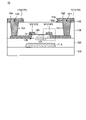
- FIG. 1 is a cross-sectional view showing an outline of a semiconductor device according to one embodiment of the present invention
- FIG. 1 is a plan view showing an outline of a semiconductor device according to one embodiment of the present invention
- FIG. 1 is a partially enlarged cross-sectional view of a semiconductor device according to an embodiment of the present invention
- FIG. 1 is a cross-sectional STEM image of a semiconductor device according to an embodiment of the present invention
- FIG. 1 is a partially enlarged cross-sectional view of a semiconductor device according to an embodiment of the present invention
- FIG. It is a sectional view showing a manufacturing method of a semiconductor device concerning one embodiment of the present invention.
- FIG. 1 is a cross-sectional TEM image of a semiconductor device according to an embodiment of the present invention
- 1 is a cross-sectional HAADF-STEM image of a semiconductor device according to an embodiment of the present invention
- FIG. 1 is a plan view showing an overview of a display device according to an embodiment of the invention
- FIG. 1 is a block diagram showing the circuit configuration of a display device according to an embodiment of the invention
- FIG. 1 is a circuit diagram showing a pixel circuit of a display device according to an embodiment of the invention
- FIG. 1 is a cross-sectional view of a display device according to an embodiment of the invention
- FIG. 1 is a plan view of a pixel electrode and a common electrode of a display device according to an embodiment of the invention
- FIG. 1 is a circuit diagram showing a pixel circuit of a display device according to an embodiment of the invention
- FIG. 1 is a cross-sectional view of a display device according to an embodiment of the invention
- FIG. 1 is a cross-sectional view of a display device according to an embodiment of the invention
- the direction from the substrate toward the oxide semiconductor layer is referred to as upward. Conversely, the direction from the oxide semiconductor layer to the substrate is called downward.
- the terms "above” and “below” are used, but for example, the substrate and the oxide semiconductor layer may be arranged in a reversed vertical relationship from that shown in the drawing.
- the expression, for example, an oxide semiconductor layer on a substrate merely describes the vertical relationship between the substrate and the oxide semiconductor layer as described above. Other members may be arranged.
- “Upper” or “lower” means the order of stacking in a structure in which a plurality of layers are stacked, and when expressing a pixel electrode above a transistor, the positional relationship is such that the transistor and the pixel electrode do not overlap in plan view. good too.
- the term “pixel electrode vertically above the transistor” means a positional relationship in which the transistor and the pixel electrode overlap in a plan view.
- Display device refers to a structure that displays images using an electro-optic layer.
- the term display device may refer to a display panel including an electro-optic layer, or to a structure in which other optical members (e.g., polarizing member, backlight, touch panel, etc.) are attached to the display cell.
- An “electro-optical layer” may include a liquid crystal layer, an electroluminescent (EL) layer, an electrochromic (EC) layer, an electrophoretic layer, unless technically contradictory. Therefore, the embodiments described later will be described by exemplifying a liquid crystal display device including a liquid crystal layer and an organic EL display device including an organic EL layer as display devices. It can be applied to a display device including an optical layer.
- ⁇ includes A, B or C
- ⁇ includes any one of A, B and C
- ⁇ includes one selected from the group consisting of A, B and C
- ⁇ does not exclude the case where ⁇ includes a plurality of combinations of A to C, unless otherwise specified.
- these expressions do not exclude the case where ⁇ contains other elements.
- FIG. 1 A semiconductor device according to an embodiment of the present invention will be described with reference to FIGS. 1 to 17.
- FIG. The semiconductor devices of the embodiments described below are used in integrated circuits (ICs) such as microprocessors (Micro-Processing Units (MPUs)) or memory circuits in addition to transistors used in display devices. good too.
- ICs integrated circuits
- MPUs Micro-Processing Units
- FIG. 1 is a cross-sectional view showing an outline of a semiconductor device according to one embodiment of the present invention.
- FIG. 2 is a plan view showing an outline of a semiconductor device according to one embodiment of the present invention.
- FIG. 3 is a partially enlarged cross-sectional view of a semiconductor device according to an embodiment of the present invention.
- the semiconductor device 10 is provided above the substrate 100 .
- the semiconductor device 10 includes a first gate electrode 110, a first gate insulating layer 120, a first oxide semiconductor layer 130, a first source electrode 141, a first drain electrode 143, a first insulating layer 150, an oxide layer 160, a first It has one source wiring 171 and a first drain wiring 173 .
- these electrodes may be referred to as a pair of first electrodes 140 or simply as the first electrodes 140 .
- the first electrodes 140 refer to a pair of first electrodes 140 unless otherwise specified.
- the first source wiring 171 and the first drain wiring 173 are not particularly distinguished, these wirings may be referred to as the first conductive layer 170 .
- a first gate electrode 110 is provided on the substrate 100 .
- the first gate electrode 110 faces the first oxide semiconductor layer 130 .
- the first gate insulating layer 120 is provided between the first gate electrode 110 and the first oxide semiconductor layer 130 .
- the first gate electrode 110 and the first gate insulating layer 120 are provided below the first oxide semiconductor layer 130 .
- the first electrode 140 is provided on the first gate insulating layer 120 and the first oxide semiconductor layer 130 .
- the first electrode 140 extends from the upper surface of the first gate insulating layer 120 to the pattern edge of the first oxide semiconductor layer 130 and continues to the upper surface of the first oxide semiconductor layer 130 . That is, the first electrode 140 is in contact with the first oxide semiconductor layer 130 from above the first oxide semiconductor layer 130 .
- the top surface of the first oxide semiconductor layer 130 can be called a first surface 137 and the bottom surface thereof can be called a second surface 138 .
- the first electrode 140 is in contact with the first surface 137 of the first oxide semiconductor layer 130 .
- the first oxide semiconductor layer 130 has a channel region 131 between the first source electrode 141 and the first drain electrode 143 .
- the first oxide semiconductor layer 130 in the channel region 131 is exposed from the first source electrode 141 and the first drain electrode 143 . That is, each of the first source electrode 141 and the first drain electrode 143 is in contact with the first oxide semiconductor layer 130 at the end of the channel region 131 .
- the first insulating layer 150 covers the first oxide semiconductor layer 130 and the first electrode 140 . Specifically, the first insulating layer 150 covers the first surface 137 of the first oxide semiconductor layer 130 sandwiched between the pair of first electrodes 140 .
- First openings 151 and 153 are provided in the first insulating layer 150 .
- the first opening 151 is an opening reaching the first source electrode 141 .
- the first opening 153 is an opening reaching the first drain electrode 143 .
- An oxide layer 160 is provided over the first insulating layer 150 .
- Second openings 161 and 163 are provided in the oxide layer 160 .
- the second opening 161 is an opening continuous with the first opening 151 .
- the second opening 163 is an opening continuous with the first opening 153 .
- the first conductive layer 170 is provided on the oxide layer 160 and inside the first openings 151 and 153 .
- the first conductive layer 170 is provided in the same region as the oxide layer 160 except for regions where the first openings 151 and 153 are present. That is, the oxide layer 160 is not provided in a region where the first conductive layer 170 is not provided in plan view, and the first insulating layer 150 is exposed from the oxide layer 160 .
- the first conductive layer 170 is in contact with the first electrode 140 at the bottoms of the first openings 151 and 153 .
- the first conductive layer 170 is electrically connected to the first oxide semiconductor layer 130 through the first electrode 140 .
- the semiconductor device 10 a configuration using a bottom-gate transistor in which a gate electrode is provided below an oxide semiconductor layer is exemplified, but the configuration is not limited to this.
- the first oxide semiconductor layer 130 is provided inside the first gate electrode 110 in plan view.
- the first oxide semiconductor layer 130 is provided inside the first gate electrode 110 in the region where the channel of the semiconductor device 10 is formed.
- the outer edge of the pattern of the first oxide semiconductor layer 130 is surrounded by the outer edge of the pattern of the first gate electrode 110 in plan view.
- the first electrode 140 crosses the first oxide semiconductor layer 130 in plan view.
- the first electrode 140 crosses the first oxide semiconductor layer 130 .
- the second opening 161 overlaps the first opening 151 in plan view.
- the second opening 163 overlaps the first opening 153 in plan view.
- FIG. 3 is an enlarged view of the area surrounded by the dotted line frame in FIG.
- a nitrogen-containing region 139 exists near the upper surface of the first oxide semiconductor layer 130 (the surface of the first oxide semiconductor layer 130 on the first insulating layer 150 side) in the channel region 131 .
- the nitrogen-containing region 139 exists within 2 nm, 3 nm, or 5 nm in the depth direction from the top surface of the first oxide semiconductor layer 130 .
- the nitrogen-containing region 139 contains nitrogen in addition to the main component elements of the first oxide semiconductor layer 130 .
- the composition ratio of nitrogen in the nitrogen-containing region 139 is 2% or more, 4% or more, or 6% or more.
- the first oxide semiconductor layer 130 is formed in a region near the end of at least one of the pair of first electrodes 140 (particularly on the first source electrode 141 side) by the first oxidation.
- the first oxide semiconductor layer 130 In the depth direction from the upper surface (first surface 137) of the semiconductor layer 130, there is a region having a nitrogen composition ratio of 2% or more within a range of 2 nanometers. With this configuration, the reliability of the semiconductor device 10 can be improved.
- the end portion of the channel region 131 on the side of the first electrode 140 and the end portion of the first electrode 140 on the side of the channel region 131 are at substantially the same position, but the configuration is not limited to this. For example, the channel region 131 and the first electrode 140 may be separated.
- a method for introducing nitrogen into the nitrogen-containing region 139 there is a method in which plasma treatment is performed while the top surface of the first oxide semiconductor layer 130 is exposed.
- a first gate electrode 110 , a first gate insulating layer 120 , a first oxide semiconductor layer 130 , and a first electrode 140 are formed over a substrate 100 , and the first electrode 140 is etched to form a first gate electrode 140 of a channel region 131 .
- the oxide semiconductor layer 130 is exposed.
- Plasma treatment using a nitrogen-containing gas is performed on the surface of the first oxide semiconductor layer 130 exposed from the first electrode 140, so that nitrogen is introduced into the vicinity of the surface of the first oxide semiconductor layer 130. be.
- the nitrogen-containing region 139 is formed by performing plasma processing using N 2 O gas (hereinafter referred to as “N 2 O plasma processing”) as the plasma processing.
- N 2 O plasma processing N 2 O gas
- the composition ratio of nitrogen in the nitrogen-containing region 139 is determined by controlling the treatment time of the N 2 O plasma treatment.
- FIG. 4 is a cross-sectional STEM (Scanning Transmission Electron Microscope) image of a semiconductor device according to an embodiment of the present invention.
- the first gate insulating layer 120 and the first insulating layer 150 are displayed in black, the first oxide semiconductor layer 130 is displayed in white, and the first electrode 140 is displayed in gray. It is
- the composition analysis of the nitrogen-containing region 139 is performed by EDX (Energy Dispersive X-ray spectrometry; energy dispersive X-ray spectrometer) provided in the STEM.
- EDX Electronicgy Dispersive X-ray spectrometry; energy dispersive X-ray spectrometer
- the STEM image shown in FIG. 4 is subjected to EDX analysis of 256 points vertically and horizontally.
- the composition ratio of the region specified by the specified line 201 and line extraction width 202 shown below is calculated.
- the equipment and measurement conditions used for STEM observation and EDX analysis of the nitrogen-containing region 139 are as follows.
- the apparatus and conditions shown below are merely examples, and the present invention is not limited to observations and analyzes conducted under the following apparatus and conditions.
- Calculation of the composition ratio is performed for each point on the designated line 201 in FIG. In the calculation performed at each point of the specified line 201, the EDX spectral data in the range specified by the line extraction width 202 are integrated.
- the analysis results below are the results of measurements performed including the first insulating layer 150, the first oxide semiconductor layer 130, and the first gate insulating layer 120, as shown in FIG.
- FIG. 5 is a diagram showing the results of composition analysis of the semiconductor device of the comparative example.
- FIG. 6 is an enlarged view of the vicinity of the boundary between the first insulating layer 150Z and the first oxide semiconductor layer 130Z in FIG.
- the horizontal axis (“Thk.”) in FIGS. 5 and 6 indicates the position of the designated line 201 in the thickness direction.
- the vertical axes in FIGS. 5 and 6 indicate the silicon composition ratio (left vertical axis) or the nitrogen composition ratio (right vertical axis).
- 5 and 6 show two types of spectra, the spectrum 219Z indicated by a relatively thick line is a spectrum indicating the composition ratio of nitrogen, and the spectrum 229Z indicated by a relatively thin line is a spectrum showing the composition ratio of silicon.
- silicon oxide is used for the first gate insulating layer 120Z and the first insulating layer 150Z
- IGZO is used for the first oxide semiconductor layer 130Z.
- the silicon composition ratio (spectrum 229Z) changes abruptly.
- Nitrogen (spectrum 219Z) is detected in the first oxide semiconductor layer 130Z. In the comparative example of FIG. 5, nitrogen is detected near the center of the first oxide semiconductor layer 130Z.
- FIG. 7 is a diagram showing the results of composition analysis of the semiconductor device according to one embodiment of the present invention.
- FIG. 8 is an enlarged view of the vicinity of the boundary between the first insulating layer 150 and the first oxide semiconductor layer 130 in FIG. In the following description, the description of points that overlap with those in FIGS. 5 and 6 will be omitted.
- nitrogen is detected near the boundary between the first insulating layer 150 and the first oxide semiconductor layer 130 in the semiconductor device 10 .
- the nitrogen composition ratio is within a range (nitrogen-containing region 139) of 2 nm or less. There is an area of about 2 percent (1.88 percent is the correct value in the graph of FIG. 8) or more.
- FIG. 9 is a diagram showing the results of composition analysis of the semiconductor device according to one embodiment of the present invention.
- the semiconductor device 10 is an enlarged view of the vicinity of the boundary between the first insulating layer 150A and the first oxide semiconductor layer 130A in FIG.
- the semiconductor device 10A has substantially the same configuration as the semiconductor device 10 shown in FIGS. 7 and 8, but the conditions for introducing nitrogen into the first oxide semiconductor layer 130A are different. As a result, the composition ratio of nitrogen in the nitrogen-containing region 139A of the semiconductor device 10A is higher than the composition ratio of nitrogen in the nitrogen-containing region 139 of the semiconductor device 10A.
- the composition ratio of nitrogen in the vicinity of the boundary between the first insulating layer 150A and the first oxide semiconductor layer 130A is the same as that of the first insulating layer 150 of the semiconductor device 10 and the first oxide semiconductor layer 130A. It is larger than the composition ratio of nitrogen in the vicinity of the boundary with the semiconductor layer 130 .
- the nitrogen composition ratio is within a range of 2 nm (the nitrogen-containing region 139A). There is an area of 6 percent or more (6.09 percent is the correct value in the graph of FIG. 10).
- FIGS. 11 to 13 are diagrams showing the results of reliability tests performed on the semiconductor devices of the comparative example and the present embodiment.
- the reliability tests shown in FIGS. 11 to 13 are tests for evaluating NBTS (Negative Bias Thermal Stress) reliability.
- the conditions for the NBTS reliability test are as follows. ⁇ Light irradiation conditions: No irradiation (dark room) ⁇ Gate voltage: -40V ⁇ Source and drain voltage: 0V ⁇ Stage temperature during stress application: 125°C
- the reason why the reliability of the semiconductor device shown in FIGS. It is believed that there is. That is, it is considered that the higher the composition ratio of nitrogen in the nitrogen-containing regions 139 and 139A, the greater the effect of improving reliability.
- Defects may occur on the upper surface of the first oxide semiconductor layer 130 due to the influence of the processes such as film formation and etching of the first electrode 140 . Although the details will be described later, it is considered that the deterioration in reliability caused by the reliability test described above is caused by defects formed on the upper surface of the first oxide semiconductor layer 130 due to the acceptor level. It is considered that introduction of nitrogen into the first oxide semiconductor layer 130 having a defect in the acceptor level reduces the acceptor level and improves the deterioration of reliability.
- FIG. 14 and 16 are diagrams showing models of simulations performed on a semiconductor device according to an embodiment of the present invention.
- 15 and 17 are diagrams showing simulation results performed on a semiconductor device according to an embodiment of the present invention.
- SiO corresponds to the first gate insulating layer 120 in FIG. 1
- OS corresponds to the first oxide semiconductor layer 130 in FIG. It corresponds to the electrode 140
- PASS corresponds to the first insulating layer 150 .
- an acceptor level defect region (defect doping) is set on the surface of the OS.
- “defect doping” is set for the OS of the entire channel region 131 and the region corresponding to the vicinity of the upper surface of the first oxide semiconductor layer 130 .
- “Defect Doping” is set only for the OS of the region corresponding to the vicinity of the end portion of the first electrode 140 (S/D) in the channel region 131 .
- FIG. 15 shows the results of a simulation performed under the conditions that "Defect Doping" is zero (STD), 5 ⁇ 10 18 cm ⁇ 2 , 5 ⁇ 10 19 cm ⁇ 2 , and 5 ⁇ 10 20 cm ⁇ 2 . .
- STD the conditions for each defect density in "Defect Doping".
- a flexible substrate containing a resin and having flexibility such as a polyimide substrate, an acrylic substrate, a siloxane substrate, or a fluororesin substrate, can be used.
- impurities may be introduced into the above resin.
- the substrate 100 does not have to be transparent, so impurities that degrade the transparency of the substrate 100 can be used.
- the substrate 100 when the substrate 100 does not need to be flexible, a rigid substrate that transmits light and does not have flexibility, such as a glass substrate, a quartz substrate, or a sapphire substrate, can be used as the substrate 100 .
- the substrate 100 may be a semiconductor substrate such as a silicon substrate, a silicon carbide substrate, or a compound semiconductor substrate, or a conductive substrate such as a stainless steel substrate having translucency. A substrate without a film can be used.
- first gate electrode 110 the first electrode 140, and the first conductive layer 170.
- these members include aluminum (Al), titanium (Ti), chromium (Cr), cobalt (Co), nickel (Ni), molybdenum (Mo), hafnium (Hf), tantalum (Ta), tungsten (W), bismuth (Bi), silver (Ag), and alloys or compounds thereof are used.
- the above materials may be used in a single layer or in a stacked layer.
- the metal element forming the first electrode 140 in contact with the first oxide semiconductor layer 130 among the first electrodes 140 is more stable than the oxide of the metal element forming the first oxide semiconductor layer 130 . That is, when there are a plurality of metal elements forming the first oxide semiconductor layer 130, the first electrode in contact with the first oxide semiconductor layer 130 is determined by the Gibbs free energy ( ⁇ G f ) of the metal oxide of each of the plurality of metal elements. It is preferable that the Gibbs free energy of the metal oxide of the metal element forming 140 is smaller.
- IGZO when IGZO is used as the first oxide semiconductor layer 130, Ti can be used as a metal in contact with IGZO.
- the Gibbs free energy of indium oxide is larger than the Gibbs free energy of each of Ga oxide and Zn oxide. In other words, indium oxide is chemically unstable and easily reduced.
- the Gibbs free energy of Ti oxide is sufficiently smaller than the Gibbs free energy of each of Ga oxide and Zn oxide, when Ti is formed on IGZO, Ti combines with oxygen in IGZO to form Ti oxide. Form. Since indium oxide is easily reduced as described above, when high energy is supplied while IGZO and Ti are in contact with each other, indium oxide is reduced and Ti is oxidized.
- Common insulating layer materials can be used as the first gate insulating layer 120 and the first insulating layer 150 .
- these insulating layers include silicon oxide (SiO x ), silicon oxynitride (SiO x N y ), silicon nitride (SiN x ), silicon oxynitride (SiN x O y ), aluminum oxide (AlO x ), oxide Inorganic insulating layers such as aluminum nitride (AlO x N y ), aluminum oxynitride (AlN x O y ), and aluminum nitride (AlN x ) can be used. An insulating layer with few defects can be used as these insulating layers.
- the composition ratio of oxygen in the first insulating layer 150 is compared with the composition ratio of oxygen in an insulating layer having the same composition as the first insulating layer 150 (hereinafter referred to as “another insulating layer”), the other The oxygen composition ratio in the first insulating layer 150 is closer to the stoichiometric ratio for the insulating layer having the same composition as the first insulating layer 150 than the oxygen composition ratio in the insulating layer.
- SiO x N y and AlO x N y are silicon compounds and aluminum compounds containing nitrogen (N) in a proportion (x>y) smaller than that of oxygen (O). Also, SiN x O y and AlN x O y are silicon compounds and aluminum compounds containing a smaller proportion of oxygen than nitrogen (x>y).
- a metal oxide having semiconductor properties can be used as the first oxide semiconductor layer 130 .
- an oxide semiconductor containing indium (In), gallium (Ga), zinc (Zn), and oxygen (O) can be used.
- the oxide semiconductor containing In, Ga, Zn, and O used in this embodiment is not limited to the above composition, and an oxide semiconductor having a composition different from the above can also be used.
- the ratio of In may be increased to improve mobility.
- the ratio of Ga may be made larger than the above in order to increase the bandgap and reduce the influence of light irradiation.
- oxide semiconductor containing In, Ga, Zn, and O may be added.
- metal elements such as Al and Sn may be added.
- an oxide semiconductor containing In and Ga (IGO), an oxide semiconductor containing In and Zn (IZO), an oxide semiconductor containing In, Sn and Zn (ITZO), and In and W can be used as the first oxide semiconductor layer 130 .
- the first oxide semiconductor layer 130 may be amorphous or crystalline.
- the first oxide semiconductor layer 130 may have a mixed phase of amorphous and crystal.
- the oxide layer 160 an oxide semiconductor layer having the same composition as the first oxide semiconductor layer 130, an oxide conductive layer such as ITO, or an oxide of SiOx , SiOxNy , AlOx , AlOxNy , or the like .
- a material insulating layer can be used.
- the oxide layer 160 is preferably formed by a sputtering method.
- the process gas used for sputtering remains in the film of the oxide layer 160 .
- Ar is used as a sputtering process gas, Ar may remain in the oxide layer 160 .
- the remaining Ar can be detected by SIMS (Secondary Ion Mass Spectrometry) analysis of the oxide layer 160 .
- SIMS Secondary Ion Mass Spectrometry
- FIG. 18 A semiconductor device according to an embodiment of the present invention will be described with reference to FIGS. 18 to 33.
- FIG. The semiconductor devices of the embodiments described below are used in integrated circuits (ICs) such as microprocessors (Micro-Processing Units (MPUs)) or memory circuits in addition to transistors used in display devices. good too.
- ICs integrated circuits
- MPUs Micro-Processing Units
- FIG. 18 is a partially enlarged cross-sectional view of a semiconductor device according to an embodiment of the present invention.
- FIG. 18 corresponds to an enlarged view of the area surrounded by the dotted line frame in FIG.
- the first electrode 140B has a first conductive layer 145B, a second conductive layer 147B, and a third conductive layer 149B.
- An oxidized portion 180B is provided at the pattern end portion of the first electrode 140B.
- the oxidation portion 180B is provided above the first oxide semiconductor layer 130B.
- the oxide portion 180B is the oxide of the first electrode 140B.
- the oxidation portion 180B includes a first oxidation portion 185B and a third oxidation portion 189B.
- the first oxide portion 185B is provided at the end of the first conductive layer 145B and is an oxide of the first conductive layer 145B.
- the third oxide portion 189B is provided at the end of the third conductive layer 149B and is an oxide of the third conductive layer 149B.
- the first oxidation portion 185B has conductivity.
- the first oxidation portion 185B is positioned closer to the channel region 131B than the pattern end of the second conductive layer 147B.
- the configuration in which the oxide of the second conductive layer 147B is not provided is exemplified, but the oxide of the second conductive layer 147B is between the first oxide portion 185B and the third oxide portion 189B.
- a second oxidation section may be provided. That is, the second oxidation portion may be provided at the end of the second conductive layer 147B.
- the second oxidation portion is formed in the manufacturing process of the semiconductor device 10B, but is removed in the subsequent process, so that the structure shown in FIG. 18 is formed.
- the first oxidation portion 185B does not have to be conductive.
- a channel region 131B, a first region 133B, and a second region 135B are provided in the first oxide semiconductor layer 130B.
- the channel region 131B is a region where the first electrode 140B is not provided above the first oxide semiconductor layer 130B.
- the oxidized portion 180B is provided above the first oxide semiconductor layer 130B in the channel region 131B. That is, the oxidized portion 180B overlaps the channel region 131B in plan view.
- the vicinity of the end of the first electrode 140B on the oxidized portion 180B side overlaps with a part of the channel region 131B in a plan view.
- the first electrode 140B does not have to overlap the channel region 131B in plan view.
- the first region 133B and the second region 135B are regions where the first electrode 140B is provided above the first oxide semiconductor layer 130B.
- the channel region 131B is a region where the first oxide semiconductor layer 130B is exposed from the first electrode 140B in plan view.
- the first region 133B and the second region 135B are regions where the first oxide semiconductor layer 130B overlaps with the first electrode 140B in plan view.
- the oxide portion 180B is not provided above the first oxide semiconductor layer 130B in the first region 133B and the second region 135B.
- the first region 133B is provided over substantially the entire region where the first oxide semiconductor layer 130B overlaps with the first electrode 140B.
- the second region 135B is provided at a position farther from the oxidation portion 180B in plan view than the first region 133B. That is, there is a region below the first electrode 140B where the second region 135B is not provided.
- the channel region 131B, first region 133B, and second region 135B are each formed from one oxide semiconductor layer. All of these regions have the same composition and the same crystal state in the state immediately after film formation. However, the composition and crystal state of the first oxide semiconductor layer 130B in each of the above regions are different due to the influence of the manufacturing process of the semiconductor device 10B.
- Indium contained in the first oxide semiconductor layer 130B is unevenly distributed in the first oxide semiconductor layer 130B in the first region 133B and the second region 135B.
- indium is not unevenly distributed in the first oxide semiconductor layer 130B in the channel region 131B.
- Whether or not indium is unevenly distributed in the first oxide semiconductor layer 130B may differ depending on the evaluation method and evaluation accuracy. If it is determined that indium is unevenly distributed in the first oxide semiconductor layer 130B in the channel region 131B, the degree of uneven distribution of indium in the first oxide semiconductor layer 130B in the channel region 131B is higher than that in the first region 133B. and the degree of uneven distribution of indium in the first oxide semiconductor layer 130B in the second region 135B is greater. The degree of uneven distribution of indium in the first oxide semiconductor layer 130B in the second region 135B is greater than the degree of uneven distribution of indium in the first oxide semiconductor layer 130B in the first region 133B.
- the degree of uneven distribution of indium is large, which means that the size of a region with a high indium concentration (high-concentration region) is large compared to other regions, or the size of crystallized indium compared to other regions ( or crystal grain size) is large.
- the degree of uneven distribution of indium can be measured, for example, by a cross-sectional TEM (Transmission Electron Microscope) image, a cross-sectional STEM (Scanning Transmission Electron Microscope) image, or a cross-sectional SEM (Scanning Electron Microscope) image. ) can be judged by the image. For example, when the contrast of the first oxide semiconductor layer 130B in the first region 133B and the second region 135B is higher than that of the first oxide semiconductor layer 130B in the channel region 131B, the first oxide semiconductor layer 130B in the channel region 131B It can be determined that the degree of uneven distribution of indium is greater in the first oxide semiconductor layer 130B in the first region 133B and the second region 135B than in the semiconductor layer 130B.
- FIGS. 19 to 22 are cross-sectional views showing a method of manufacturing a semiconductor device according to one embodiment of the present invention.
- the manufacturing method an example in which Ti is used for the first conductive layer 145B and the third conductive layer 149B and Al is used for the second conductive layer 147B will be described.
- the pattern of the first oxide semiconductor layer 130B is formed on the first gate insulating layer 120B provided on the first gate electrode 110B (see FIG. 1), and the pattern of the first electrode 140B is formed. form a pattern.
- a pattern end portion of the first electrode 140B is located on the first oxide semiconductor layer 130B. Since a general semiconductor process can be used for the manufacturing method up to the structure shown in FIG. 19, detailed description thereof will be omitted.
- N 2 O plasma treatment is performed as the plasma treatment.
- the N 2 O plasma treatment is performed on at least the pattern edge of the first electrode 140B.
- an oxidized portion 180B is formed at the end of the first electrode 140B by the N 2 O plasma treatment.
- the first oxidized portion 185B is formed at the end of the first conductive layer 145B
- the second oxidized portion 187B is formed at the end of the second conductive layer 147B
- the end of the third conductive layer 149B is formed.
- a third oxidation portion 189B is formed.
- the upper portion of the third conductive layer 149B which is the uppermost layer of the first electrode 140B, is also oxidized by the N 2 O plasma treatment, it is omitted for convenience of explanation.
- the second oxidized portion 187B of the oxidized portion 180B disappears in the process until the first insulating layer 150B covering the first electrode 140B is formed. As a result, as shown in FIG. 22, only the first oxidized portion 185B and the third oxidized portion 189B remain at the end of the first electrode 140B.
- the first insulating layer 150B may be formed over the structure of FIG. 21 without the second oxidation portion 187B disappearing.
- indium is segregated in the first oxide semiconductor layer 130B in a region overlapping with the first electrode 140B in plan view.
- FIGS. 23 to 28 are cross-sectional images of the samples before the reliability test is performed after the semiconductor device 10B is manufactured.
- FIG. 23 is a cross-sectional TEM image of a semiconductor device according to one embodiment of the present invention.
- Ti was used for the first conductive layer 145B and the third conductive layer 149B
- Al was used for the second conductive layer 147B
- IGZO was used for the first oxide semiconductor layer 130B. Structures are shown.
- the first conductive layer 145B (Ti) and the second conductive layer 147B (Al) have different patterns in a cross-sectional view due to their different crystal states.
- the region over which the first electrode 140B is not provided is the channel region 131B
- the regions over which the first electrode 140B is provided are the first region 133B and the second region 135B. corresponds to A mixed crystal region is formed by reaction of Ti and Al between the first conductive layer 145B and the second conductive layer 147B.
- the dotted line connecting the first conductive layer 145B and the third conductive layer 149B is the location where the end of the second conductive layer 147B is presumed to have existed based on the shapes of these conductive layers. As described above, at least part of the second conductive layer 147B disappears, resulting in a shape as shown in FIG.
- FIG. 24 is a cross-sectional HAADF (High-Angle Annular Dark Field)-STEM image of a semiconductor device according to one embodiment of the present invention.
- FIG. 24 is an enlarged STEM image of a part of FIG.
- FIG. 24 shows part of the first oxide semiconductor layer 130B, the first conductive layer 145B, and the second conductive layer 147B.
- 25 to 28 are EDX mapping measurement results of the semiconductor device according to one embodiment of the present invention.
- FIG. 25 shows the EDX mapping measurement results of Ti.
- FIG. 26 shows the EDX mapping measurement result of O.
- FIG. FIG. 27 shows the EDX mapping measurement results of In.
- FIG. 28 shows the EDX mapping measurement results of Al.
- regions where the first oxide semiconductor layer 130B, the first conductive layer 145B, and the second conductive layer 147B are provided are indicated by dotted lines.
- Ti is detected from the area surrounded by the dotted line indicating the first conductive layer 145B, but near the left end of the dotted line, the signal intensity of Ti is smaller than other areas. , the signal intensity of oxygen is large. That is, a first oxidation portion 185B (Ti oxide) is formed at the left end of the first conductive layer 145B.
- the first oxidized portion 185B has a partially chipped shape (concave shape in this embodiment). 25 and 26, oxygen is detected from the lower region of the first conductive layer 145B. That is, Ti oxide is formed under Ti.
- dark region 210B in the contrast of the STEM image in FIG. is a region with a high concentration of A region darker than other regions in FIG. 24 (hereinafter referred to as “dark region 210B”) is a region having a lower indium concentration than other regions as shown in FIG.
- the size of the cluster of bright regions 200B in the second region 135B is larger than the size of the cluster of bright regions 200B in the first region 133B.
- the channel region 131B no distinct clusters of bright regions 200B and dark regions 210B are observed, so it is determined that indium is not unevenly distributed.
- a bright region with a small size is also confirmed in the first region 133B, but this is because oxygen in the oxide semiconductor is reduced in the surface layer of the first oxide semiconductor layer 130B during the film formation of Ti or in a process after the Ti film formation. , it is considered that a region with a high concentration of indium was partially formed.
- the degree of uneven distribution of indium in the first oxide semiconductor layer 130B in the channel region 131B is higher than the degree of uneven distribution of indium in the first oxide semiconductor layer 130B in the first region 133B and the second region 135B.
- the indium of the first oxide semiconductor layer 130B is not unevenly distributed in the region overlapping with the first oxide portion 185B in plan view.
- the degree of uneven distribution of indium in the first oxide semiconductor layer 130B in the second region 135B is greater than the degree of uneven distribution of indium in the first oxide semiconductor layer 130B in the first region 133B.
- the uneven distribution of indium is caused by the crystallization of indium. Therefore, the crystal grain size of indium unevenly distributed in the first oxide semiconductor layer 130B in the second region 135B is larger than the crystal grain size of indium unevenly distributed in the first oxide semiconductor layer 130B in the first region 133B. be able to.
- the region where indium is unevenly distributed in the second region 135B does not reach the end of the first conductive layer 145B on the side of the channel region 131B. In other words, in this state, an abnormality in rising of the ON current of the semiconductor device 10B does not occur.
- the area in which oxygen is not detected and the area in which Al is detected substantially match.
- Al oxide on the order of several nanometers exists at the end of the second conductive layer 147B.
- FIG. 29 to 33 A display device using a semiconductor device according to an embodiment of the present invention will be described with reference to FIGS. 29 to 33.
- FIG. 29 to 33 configurations in which the semiconductor devices described in the first and second embodiments are applied to a circuit of a liquid crystal display device will be described.
- FIG. 29 is a plan view showing an outline of a display device according to one embodiment of the invention.
- the display device 20C has an array substrate 300C, a sealing portion 400C, a counter substrate 500C, a flexible printed circuit board 600C (FPC600C), and an IC chip 700C.
- the array substrate 300C and the counter substrate 500C are bonded together by a seal portion 400C.
- a plurality of pixel circuits 310C are arranged in a matrix in the liquid crystal region 22C surrounded by the seal portion 400C.
- the liquid crystal region 22C is a region that overlaps with a liquid crystal element 410C, which will be described later, in plan view.
- the seal region 24C provided with the seal portion 400C is the region surrounding the liquid crystal region 22C.
- the FPC 600C is provided in the terminal area 26C.
- the terminal area 26C is an area where the array substrate 300C is exposed from the counter substrate 500C, and is provided outside the seal area 24C.
- the outside of the sealing area 24C means the outside of the area where the sealing portion 400C is provided and the area surrounded by the sealing portion 400C.
- IC chip 700C is provided on FPC 600C.
- the IC chip 700C supplies signals for driving each pixel circuit 310C.
- FIG. 30 is a block diagram showing the circuit configuration of the display device according to one embodiment of the invention.
- a source driver circuit 320C is provided at a position adjacent to the liquid crystal region 22C in which the pixel circuit 310C is arranged in the D1 direction (column direction).
- a gate driver circuit 330C is provided at a position adjacent (in the row direction).
- a source driver circuit 320C and a gate driver circuit 330C are provided in the seal region 24C.
- the region where the source driver circuit 320C and the gate driver circuit 330C are provided is not limited to the seal region 24C, and may be any region outside the region where the pixel circuit 310C is provided.
- a source wiring 321C extends in the D1 direction from the source driver circuit 320C and is connected to a plurality of pixel circuits 310C arranged in the D1 direction.
- a gate wiring 331C extends in the D2 direction from the gate driver circuit 330C and is connected to a plurality of pixel circuits 310C arranged in the D2 direction.
- a terminal portion 333C is provided in the terminal region 26C.
- the terminal portion 333C and the source driver circuit 320C are connected by a connection wiring 341C.
- the terminal portion 333C and the gate driver circuit 330C are connected by a connection wiring 341C.
- the semiconductor devices 10 and 10A shown in the first and second embodiments are applied to transistors included in the pixel circuit 310C, source driver circuit 320C, and gate driver circuit 330C.
- FIG. 31 is a circuit diagram showing a pixel circuit of a display device according to one embodiment of the invention.
- pixel circuit 310C includes elements such as transistor 800C, storage capacitor 890C, and liquid crystal element 410C.
- Transistor 800C has a first gate electrode 810C, a first source electrode 830C, and a first drain electrode 840C.
- the first gate electrode 810C is connected to the gate wiring 331C.
- the first source electrode 830C is connected to the source wiring 321C.
- the first drain electrode 840C is connected to the storage capacitor 890C and the liquid crystal element 410C.
- the semiconductor devices 10 and 10A shown in the first and second embodiments are applied to the transistor shown in FIG.
- 830C is referred to as a source electrode and 840C is referred to as a drain electrode, but the source and drain functions of each electrode may be interchanged.
- FIG. 32 is a cross-sectional view of a display device according to an embodiment of the invention.
- the display device 20C is a display device provided with transistors 800C and 900C having different structures on the same substrate.
- the structure of transistor 800C differs from that of transistor 900C.
- the transistor 800C is a bottom-gate transistor in which the first oxide semiconductor layer 820C is used as a channel.
- the transistor 900C is a top-gate transistor using the semiconductor layer 920C as a channel.
- transistor 800C is used in pixel circuit 310C
- transistor 900C is used in source driver circuit 320C and gate driver circuit 330C. Note that the transistor 900C may be used in the pixel circuit 310C.
- the transistor 800C is a transistor formed on the substrate 301C and having one or more insulating layers as a base layer.
- the insulating layers 340C, 342C, 344C, and 346C are used as underlying layers.
- a first gate electrode 810C is provided on the insulating layer 346C.
- a first oxide semiconductor layer 820C is provided above the first gate electrode 810C.
- the first gate electrode 810C faces the first oxide semiconductor layer 820C.
- An insulating layer 348C functioning as a gate insulating layer is provided between the first gate electrode 810C and the first oxide semiconductor layer 820C.
- a first source electrode 830C is provided at one end of the pattern of the first oxide semiconductor layer 820C, and a first drain electrode 840C is provided at the other end.
- the first source electrode 830C and the first drain electrode 840C are connected to the first oxide semiconductor layer 820C on the top and side surfaces of the first oxide semiconductor layer 820C, respectively.
- First insulating layers 350C and 352C are provided on the first oxide semiconductor layer 820C, the first source electrode 830C, and the first drain electrode 840C. Openings 851C and 861C are provided in the first insulating layers 350C and 352C.
- a first source wiring 850C is provided on the first insulating layer 352C and inside the opening 851C.
- a first drain wiring 860C is provided on the first insulating layer 352C and inside the opening 861C.
- An oxide layer 853C is provided between the upper surface of the first insulating layer 352C and the first source wiring 850C.
- An oxide layer 855C is provided between the upper surface of the first insulating layer 352C and the first drain wiring 860C.
- a second insulating layer 354C is provided on the first source wiring 850C and the first drain wiring 860C.
- a common electrode 880C provided in common to a plurality of pixels is provided on the second insulating layer 354C.
- a second insulating layer 356C is provided on the common electrode 880C.
- a third opening 871C is provided in the second insulating layers 354C and 356C.
- a pixel electrode 870C is provided on the second insulating layer 356C and inside the third opening 871C. The pixel electrode 870C is connected to the first drain wiring 860C.
- FIG. 33 is a plan view of a pixel electrode and a common electrode of a display device according to one embodiment of the invention.
- the common electrode 880C has an overlapping region that overlaps the pixel electrode 870C in plan view and a non-overlapping region that does not overlap the pixel electrode 870C.
- a horizontal electric field is formed from the pixel electrode 870C in the overlapping area toward the common electrode 880C in the non-overlapping area.
- the horizontal electric field causes the liquid crystal molecules contained in the liquid crystal element 410C to operate, thereby determining the gradation of the pixel.
- the semiconductor device 10 of FIG. 1 can be applied as the transistor 800C.
- each member in each drawing corresponds as follows.
- the first gate electrode 110 corresponds to the first gate electrode 810C.
- the first gate insulating layer 120 corresponds to the insulating layer 348C.
- the first oxide semiconductor layer 130 corresponds to the first oxide semiconductor layer 820C.
- the first source electrode 141 corresponds to the first source electrode 830C.
- the first drain electrode 143 corresponds to the first drain electrode 840C.
- the first insulating layer 150 corresponds to the first insulating layers 350C and 352C.
- the first opening 151 corresponds to the opening 851C.
- the first opening 153 corresponds to the opening 861C.
- Oxide layer 160 corresponds to oxide layers 853C and 855C.
- the first source wiring 171 corresponds to the first source wiring 850C.
- the first drain wiring 173 corresponds to the first drain wiring 860C.
- the transistor 900C is a transistor formed on the substrate 301C and having an insulating layer 340C as a base layer.
- a light shielding layer 910C is provided on the insulating layer 340C.
- An insulating layer 342C is provided on the light shielding layer 910C.
- a semiconductor layer 920C is provided over the insulating layer 342C.
- a second gate electrode 930C is provided above the semiconductor layer 920C.
- An insulating layer 344C functioning as a gate insulating layer is provided between the semiconductor layer 920C and the second gate electrode 930C. Insulating layers 346C, 348C, 350C, and 352C are provided on the second gate electrode 930C. Openings 941C and 951C are provided in these insulating layers.
- a second source wiring 940C is provided on the insulating layer 352C and inside the opening 941C.
- a second drain wiring 950C is provided on the insulating layer 352C and inside the opening 951C.
- An insulating layer 354C is provided over the second source wiring 940C and the second drain wiring 950C.
- the second gate electrode 930C is provided under the same layer (insulating layer 348C) as the gate insulating layer of the transistor 800C.
- FIG. 34 A display device using a semiconductor device according to an embodiment of the present invention will be described with reference to FIGS. 34 and 35.
- FIG. 34 configurations in which the semiconductor devices described in the first and second embodiments are applied to the circuit of an organic EL display device will be described. Note that the outline and circuit configuration of the display device 20D are the same as those shown in FIGS. 29 and 30, so description thereof will be omitted.
- FIG. 34 is a circuit diagram showing a pixel circuit of a display device according to one embodiment of the invention.
- the pixel circuit 310D includes elements such as a drive transistor 960D, a selection transistor 970D, a storage capacitor 980D, and a light emitting element DO.
- a source electrode of the selection transistor 970D is connected to the signal line 971D, and a gate electrode of the selection transistor 970D is connected to the gate line 973D.
- a source electrode of the drive transistor 960D is connected to the anode power supply line 961D, and a drain electrode of the drive transistor 960D is connected to one end of the light emitting element DO.
- the other end of the light emitting element DO is connected to the cathode power line 963D.
- a gate electrode of the drive transistor 960D is connected to a drain electrode of the selection transistor 970D.
- the storage capacitor 980D is connected to the gate and drain electrodes of the driving transistor 960D.
- a gradation signal that determines the light emission intensity of the light emitting element DO is supplied to the signal line 971D.
- the gate line 973D is supplied with a signal for selecting a pixel row to which the grayscale signal is written.
- FIG. 35 is a cross-sectional view of a display device according to an embodiment of the invention.
- the configuration of the display device 20D shown in FIG. 35 is similar to that of the display device 20C shown in FIG. differ from 35, the same configuration as that of the display device 20C shown in FIG. 32 will be omitted, and the differences from the display device 20C will be explained.
- the display device 20D has a pixel electrode 981D, a light emitting layer 983D, and a common electrode 985D above the insulating layer 354D.
- a pixel electrode 981D is provided on the insulating layer 354D and inside the third opening 871D.
- An insulating layer 358D is provided over the pixel electrode 981D.
- An opening 359D is provided in the insulating layer 358D. Opening 359D corresponds to the light emitting area. That is, the insulating layer 358D defines pixels.
- a light emitting layer 983D and a common electrode 985D are provided on the pixel electrode 981D exposed by the opening 359D.
- a pixel electrode 981D and a light-emitting layer 983D are individually provided for each pixel.
- the common electrode 985D is commonly provided for a plurality of pixels. Different materials are used for the light-emitting layer 983D depending on the display color of the pixel.
- the configurations in which the semiconductor devices described in the first and second embodiments are applied to the liquid crystal display device and the organic EL display device are exemplified.
- the semiconductor device may be applied to a device (for example, a self-luminous display device other than an organic EL display device or an electronic paper display device).
- the above semiconductor device can be applied to a medium-sized display device to a large-sized display device without particular limitation.
Landscapes
- Thin Film Transistor (AREA)
- Engineering & Computer Science (AREA)
- Manufacturing & Machinery (AREA)
Priority Applications (2)
| Application Number | Priority Date | Filing Date | Title |
|---|---|---|---|
| JP2023500644A JPWO2022176484A1 (https=) | 2021-02-17 | 2022-01-19 | |
| US18/449,830 US20230387322A1 (en) | 2021-02-17 | 2023-08-15 | Semiconductor device |
Applications Claiming Priority (2)
| Application Number | Priority Date | Filing Date | Title |
|---|---|---|---|
| JP2021023751 | 2021-02-17 | ||
| JP2021-023751 | 2021-02-17 |
Related Child Applications (1)
| Application Number | Title | Priority Date | Filing Date |
|---|---|---|---|
| US18/449,830 Continuation US20230387322A1 (en) | 2021-02-17 | 2023-08-15 | Semiconductor device |
Publications (1)
| Publication Number | Publication Date |
|---|---|
| WO2022176484A1 true WO2022176484A1 (ja) | 2022-08-25 |
Family
ID=82930777
Family Applications (1)
| Application Number | Title | Priority Date | Filing Date |
|---|---|---|---|
| PCT/JP2022/001713 Ceased WO2022176484A1 (ja) | 2021-02-17 | 2022-01-19 | 半導体装置 |
Country Status (3)
| Country | Link |
|---|---|
| US (1) | US20230387322A1 (https=) |
| JP (1) | JPWO2022176484A1 (https=) |
| WO (1) | WO2022176484A1 (https=) |
Cited By (1)
| Publication number | Priority date | Publication date | Assignee | Title |
|---|---|---|---|---|
| CN119783610A (zh) * | 2023-10-07 | 2025-04-08 | 中国科学院沈阳自动化研究所 | 抗辐照正方环栅mosfet半导体器件建模方法 |
Citations (6)
| Publication number | Priority date | Publication date | Assignee | Title |
|---|---|---|---|---|
| JP2011142310A (ja) * | 2009-12-08 | 2011-07-21 | Semiconductor Energy Lab Co Ltd | 半導体装置およびその作製方法 |
| JP2012134472A (ja) * | 2010-11-30 | 2012-07-12 | Semiconductor Energy Lab Co Ltd | 半導体装置およびその作製方法 |
| JP2014007393A (ja) * | 2012-05-31 | 2014-01-16 | Semiconductor Energy Lab Co Ltd | 半導体装置およびその作製方法 |
| US20140231810A1 (en) * | 2013-02-21 | 2014-08-21 | Samsung Display Co., Ltd. | Thin film transistor and manufacturing method thereof |
| JP2018022879A (ja) * | 2016-07-20 | 2018-02-08 | 株式会社リコー | 電界効果型トランジスタ、及びその製造方法、並びに表示素子、画像表示装置、及びシステム |
| JP2020167235A (ja) * | 2019-03-28 | 2020-10-08 | 株式会社ジャパンディスプレイ | 半導体装置 |
Family Cites Families (1)
| Publication number | Priority date | Publication date | Assignee | Title |
|---|---|---|---|---|
| US20130087784A1 (en) * | 2011-10-05 | 2013-04-11 | Semiconductor Energy Laboratory Co., Ltd. | Semiconductor device and manufacturing method thereof |
-
2022
- 2022-01-19 JP JP2023500644A patent/JPWO2022176484A1/ja active Pending
- 2022-01-19 WO PCT/JP2022/001713 patent/WO2022176484A1/ja not_active Ceased
-
2023
- 2023-08-15 US US18/449,830 patent/US20230387322A1/en active Pending
Patent Citations (6)
| Publication number | Priority date | Publication date | Assignee | Title |
|---|---|---|---|---|
| JP2011142310A (ja) * | 2009-12-08 | 2011-07-21 | Semiconductor Energy Lab Co Ltd | 半導体装置およびその作製方法 |
| JP2012134472A (ja) * | 2010-11-30 | 2012-07-12 | Semiconductor Energy Lab Co Ltd | 半導体装置およびその作製方法 |
| JP2014007393A (ja) * | 2012-05-31 | 2014-01-16 | Semiconductor Energy Lab Co Ltd | 半導体装置およびその作製方法 |
| US20140231810A1 (en) * | 2013-02-21 | 2014-08-21 | Samsung Display Co., Ltd. | Thin film transistor and manufacturing method thereof |
| JP2018022879A (ja) * | 2016-07-20 | 2018-02-08 | 株式会社リコー | 電界効果型トランジスタ、及びその製造方法、並びに表示素子、画像表示装置、及びシステム |
| JP2020167235A (ja) * | 2019-03-28 | 2020-10-08 | 株式会社ジャパンディスプレイ | 半導体装置 |
Cited By (1)
| Publication number | Priority date | Publication date | Assignee | Title |
|---|---|---|---|---|
| CN119783610A (zh) * | 2023-10-07 | 2025-04-08 | 中国科学院沈阳自动化研究所 | 抗辐照正方环栅mosfet半导体器件建模方法 |
Also Published As
| Publication number | Publication date |
|---|---|
| JPWO2022176484A1 (https=) | 2022-08-25 |
| US20230387322A1 (en) | 2023-11-30 |
Similar Documents
| Publication | Publication Date | Title |
|---|---|---|
| US20220045216A1 (en) | Semiconductor device | |
| WO2022176484A1 (ja) | 半導体装置 | |
| US11342463B2 (en) | Semiconductor device and manufacturing method of semiconductor device | |
| US20240429320A1 (en) | Array substrate | |
| KR102801339B1 (ko) | 반도체 장치 | |
| KR102898869B1 (ko) | 반도체 장치 | |
| KR102870475B1 (ko) | 반도체 장치 | |
| KR102733354B1 (ko) | 반도체 장치의 제조 방법 | |
| KR102947178B1 (ko) | 반도체 장치 | |
| TWI841307B (zh) | 半導體裝置之製造方法 | |
| KR102955752B1 (ko) | 반도체 장치 및 그 제조 방법 | |
| CN118872073A (zh) | 半导体装置 | |
| JP2021057461A (ja) | 半導体装置及び半導体装置の製造方法 | |
| WO2023189493A1 (ja) | 半導体装置 | |
| KR20230141493A (ko) | 반도체 장치의 제조 방법 | |
| KR20250136388A (ko) | 반도체 장치 | |
| CN118872072A (zh) | 半导体装置 | |
| JPWO2023189487A5 (https=) | ||
| JP2024040960A5 (https=) |
Legal Events
| Date | Code | Title | Description |
|---|---|---|---|
| 121 | Ep: the epo has been informed by wipo that ep was designated in this application |
Ref document number: 22755809 Country of ref document: EP Kind code of ref document: A1 |
|
| WWE | Wipo information: entry into national phase |
Ref document number: 2023500644 Country of ref document: JP |
|
| NENP | Non-entry into the national phase |
Ref country code: DE |
|
| 122 | Ep: pct application non-entry in european phase |
Ref document number: 22755809 Country of ref document: EP Kind code of ref document: A1 |