WO2022176451A1 - 半導体装置、半導体装置の製造方法 - Google Patents
半導体装置、半導体装置の製造方法 Download PDFInfo
- Publication number
- WO2022176451A1 WO2022176451A1 PCT/JP2022/000909 JP2022000909W WO2022176451A1 WO 2022176451 A1 WO2022176451 A1 WO 2022176451A1 JP 2022000909 W JP2022000909 W JP 2022000909W WO 2022176451 A1 WO2022176451 A1 WO 2022176451A1
- Authority
- WO
- WIPO (PCT)
- Prior art keywords
- semiconductor chip
- semiconductor device
- heat
- wiring board
- exhaust member
- Prior art date
- Legal status (The legal status is an assumption and is not a legal conclusion. Google has not performed a legal analysis and makes no representation as to the accuracy of the status listed.)
- Ceased
Links
Images




Classifications
-
- H—ELECTRICITY
- H10—SEMICONDUCTOR DEVICES; ELECTRIC SOLID-STATE DEVICES NOT OTHERWISE PROVIDED FOR
- H10F—INORGANIC SEMICONDUCTOR DEVICES SENSITIVE TO INFRARED RADIATION, LIGHT, ELECTROMAGNETIC RADIATION OF SHORTER WAVELENGTH OR CORPUSCULAR RADIATION
- H10F39/00—Integrated devices, or assemblies of multiple devices, comprising at least one element covered by group H10F30/00, e.g. radiation detectors comprising photodiode arrays
- H10F39/80—Constructional details of image sensors
- H10F39/804—Containers or encapsulations
-
- H—ELECTRICITY
- H10—SEMICONDUCTOR DEVICES; ELECTRIC SOLID-STATE DEVICES NOT OTHERWISE PROVIDED FOR
- H10W—GENERIC PACKAGES, INTERCONNECTIONS, CONNECTORS OR OTHER CONSTRUCTIONAL DETAILS OF DEVICES COVERED BY CLASS H10
- H10W40/00—Arrangements for thermal protection or thermal control
- H10W40/20—Arrangements for cooling
- H10W40/25—Arrangements for cooling characterised by their materials
- H10W40/251—Organics
-
- H—ELECTRICITY
- H10—SEMICONDUCTOR DEVICES; ELECTRIC SOLID-STATE DEVICES NOT OTHERWISE PROVIDED FOR
- H10W—GENERIC PACKAGES, INTERCONNECTIONS, CONNECTORS OR OTHER CONSTRUCTIONAL DETAILS OF DEVICES COVERED BY CLASS H10
- H10W40/00—Arrangements for thermal protection or thermal control
- H10W40/70—Fillings or auxiliary members in containers or in encapsulations for thermal protection or control
-
- H—ELECTRICITY
- H10—SEMICONDUCTOR DEVICES; ELECTRIC SOLID-STATE DEVICES NOT OTHERWISE PROVIDED FOR
- H10W—GENERIC PACKAGES, INTERCONNECTIONS, CONNECTORS OR OTHER CONSTRUCTIONAL DETAILS OF DEVICES COVERED BY CLASS H10
- H10W40/00—Arrangements for thermal protection or thermal control
- H10W40/70—Fillings or auxiliary members in containers or in encapsulations for thermal protection or control
- H10W40/73—Fillings or auxiliary members in containers or in encapsulations for thermal protection or control for cooling by change of state
-
- H—ELECTRICITY
- H10—SEMICONDUCTOR DEVICES; ELECTRIC SOLID-STATE DEVICES NOT OTHERWISE PROVIDED FOR
- H10W—GENERIC PACKAGES, INTERCONNECTIONS, CONNECTORS OR OTHER CONSTRUCTIONAL DETAILS OF DEVICES COVERED BY CLASS H10
- H10W70/00—Package substrates; Interposers; Redistribution layers [RDL]
- H10W70/60—Insulating or insulated package substrates; Interposers; Redistribution layers
- H10W70/67—Insulating or insulated package substrates; Interposers; Redistribution layers characterised by their insulating layers or insulating parts
- H10W70/68—Shapes or dispositions thereof
-
- H—ELECTRICITY
- H10—SEMICONDUCTOR DEVICES; ELECTRIC SOLID-STATE DEVICES NOT OTHERWISE PROVIDED FOR
- H10W—GENERIC PACKAGES, INTERCONNECTIONS, CONNECTORS OR OTHER CONSTRUCTIONAL DETAILS OF DEVICES COVERED BY CLASS H10
- H10W72/00—Interconnections or connectors in packages
- H10W72/50—Bond wires
-
- H—ELECTRICITY
- H10—SEMICONDUCTOR DEVICES; ELECTRIC SOLID-STATE DEVICES NOT OTHERWISE PROVIDED FOR
- H10W—GENERIC PACKAGES, INTERCONNECTIONS, CONNECTORS OR OTHER CONSTRUCTIONAL DETAILS OF DEVICES COVERED BY CLASS H10
- H10W74/00—Encapsulations, e.g. protective coatings
- H10W74/40—Encapsulations, e.g. protective coatings characterised by their materials
- H10W74/47—Encapsulations, e.g. protective coatings characterised by their materials comprising organic materials, e.g. plastics or resins
-
- H—ELECTRICITY
- H10—SEMICONDUCTOR DEVICES; ELECTRIC SOLID-STATE DEVICES NOT OTHERWISE PROVIDED FOR
- H10W—GENERIC PACKAGES, INTERCONNECTIONS, CONNECTORS OR OTHER CONSTRUCTIONAL DETAILS OF DEVICES COVERED BY CLASS H10
- H10W76/00—Containers; Fillings or auxiliary members therefor; Seals
- H10W76/10—Containers or parts thereof
- H10W76/12—Containers or parts thereof characterised by their shape
- H10W76/15—Containers comprising an insulating or insulated base
-
- H—ELECTRICITY
- H10—SEMICONDUCTOR DEVICES; ELECTRIC SOLID-STATE DEVICES NOT OTHERWISE PROVIDED FOR
- H10W—GENERIC PACKAGES, INTERCONNECTIONS, CONNECTORS OR OTHER CONSTRUCTIONAL DETAILS OF DEVICES COVERED BY CLASS H10
- H10W76/00—Containers; Fillings or auxiliary members therefor; Seals
- H10W76/10—Containers or parts thereof
- H10W76/12—Containers or parts thereof characterised by their shape
- H10W76/15—Containers comprising an insulating or insulated base
- H10W76/153—Containers comprising an insulating or insulated base having interconnections in passages through the insulating or insulated base
-
- H—ELECTRICITY
- H10—SEMICONDUCTOR DEVICES; ELECTRIC SOLID-STATE DEVICES NOT OTHERWISE PROVIDED FOR
- H10W—GENERIC PACKAGES, INTERCONNECTIONS, CONNECTORS OR OTHER CONSTRUCTIONAL DETAILS OF DEVICES COVERED BY CLASS H10
- H10W72/00—Interconnections or connectors in packages
- H10W72/30—Die-attach connectors
-
- H—ELECTRICITY
- H10—SEMICONDUCTOR DEVICES; ELECTRIC SOLID-STATE DEVICES NOT OTHERWISE PROVIDED FOR
- H10W—GENERIC PACKAGES, INTERCONNECTIONS, CONNECTORS OR OTHER CONSTRUCTIONAL DETAILS OF DEVICES COVERED BY CLASS H10
- H10W72/00—Interconnections or connectors in packages
- H10W72/851—Dispositions of multiple connectors or interconnections
-
- H—ELECTRICITY
- H10—SEMICONDUCTOR DEVICES; ELECTRIC SOLID-STATE DEVICES NOT OTHERWISE PROVIDED FOR
- H10W—GENERIC PACKAGES, INTERCONNECTIONS, CONNECTORS OR OTHER CONSTRUCTIONAL DETAILS OF DEVICES COVERED BY CLASS H10
- H10W72/00—Interconnections or connectors in packages
- H10W72/851—Dispositions of multiple connectors or interconnections
- H10W72/874—On different surfaces
- H10W72/884—Die-attach connectors and bond wires
-
- H—ELECTRICITY
- H10—SEMICONDUCTOR DEVICES; ELECTRIC SOLID-STATE DEVICES NOT OTHERWISE PROVIDED FOR
- H10W—GENERIC PACKAGES, INTERCONNECTIONS, CONNECTORS OR OTHER CONSTRUCTIONAL DETAILS OF DEVICES COVERED BY CLASS H10
- H10W76/00—Containers; Fillings or auxiliary members therefor; Seals
- H10W76/40—Fillings or auxiliary members in containers, e.g. centering rings
- H10W76/42—Fillings
- H10W76/47—Solid or gel fillings
-
- H—ELECTRICITY
- H10—SEMICONDUCTOR DEVICES; ELECTRIC SOLID-STATE DEVICES NOT OTHERWISE PROVIDED FOR
- H10W—GENERIC PACKAGES, INTERCONNECTIONS, CONNECTORS OR OTHER CONSTRUCTIONAL DETAILS OF DEVICES COVERED BY CLASS H10
- H10W90/00—Package configurations
- H10W90/701—Package configurations characterised by the relative positions of pads or connectors relative to package parts
- H10W90/731—Package configurations characterised by the relative positions of pads or connectors relative to package parts of die-attach connectors
- H10W90/734—Package configurations characterised by the relative positions of pads or connectors relative to package parts of die-attach connectors between a chip and a stacked insulating package substrate, interposer or RDL
-
- H—ELECTRICITY
- H10—SEMICONDUCTOR DEVICES; ELECTRIC SOLID-STATE DEVICES NOT OTHERWISE PROVIDED FOR
- H10W—GENERIC PACKAGES, INTERCONNECTIONS, CONNECTORS OR OTHER CONSTRUCTIONAL DETAILS OF DEVICES COVERED BY CLASS H10
- H10W90/00—Package configurations
- H10W90/701—Package configurations characterised by the relative positions of pads or connectors relative to package parts
- H10W90/751—Package configurations characterised by the relative positions of pads or connectors relative to package parts of bond wires
- H10W90/754—Package configurations characterised by the relative positions of pads or connectors relative to package parts of bond wires between a chip and a stacked insulating package substrate, interposer or RDL
Definitions
- the present technology relates to a semiconductor device and a manufacturing method thereof. and a wiring board portion formed with external connection terminals for electrical connection with the outside, and the semiconductor chip is connected to the wiring board portion by bonding wires to the terminals formed on the surface side of the wiring board portion.
- TECHNICAL FIELD The present invention relates to a semiconductor device wire-bonded with a wire and a manufacturing method thereof.
- a semiconductor chip on which various electronic circuit components such as a transistor are formed is placed in a box-like housing formed by a wiring substrate portion, a frame portion, and a lid portion.
- the wiring substrate portion is a portion in which wiring is formed to enable signal exchange between the semiconductor chip and an external device.
- the semiconductor chip is electrically connected to the wiring substrate portion by wire bonding to terminals formed on the surface of the wiring substrate portion, that is, the surface on which the semiconductor chip is mounted.
- Conventional cooling techniques for semiconductor devices include, for example, placing a cooling block on the back side of a semiconductor chip (see, for example, Patent Document 1 below) or placing a Peltier element (see, for example, Patent Document 2 below). (see ).
- This technology has been developed in view of the above circumstances, and aims to prevent semiconductor devices from becoming large due to cooling.
- a semiconductor device includes a semiconductor chip, the semiconductor chip mounted thereon, and an electrical connection with the outside on the back surface side opposite to the surface on which the semiconductor chip is mounted.
- a wiring substrate portion formed with external connection terminals for performing the semiconductor chip, and the semiconductor chip is connected to the terminal formed on the front surface side of the wiring substrate portion by a bonding wire, and is connected to the wiring substrate portion by a wire. It is bonded, and a heat exhaust member is arranged between the bonding wire and the wiring board portion.
- a heat exhaust member means a member that forms at least a part of a heat exhaust path for cooling heat generated in a semiconductor chip. According to the above configuration, the heat exhaust member is arranged in the vicinity of the semiconductor chip serving as a heat source. In this case, the semiconductor device can be cooled by a heat exhaust member arranged in the dead space below the bonding wires.
- At least part of the heat exhaust member may be in contact with the side surface of the semiconductor chip. This improves the efficiency of heat conduction from the semiconductor chip to the heat exhaust member.
- the heat exhaust member may be configured by a heat pipe.
- heat pipe as used herein means a heat conductor in which a refrigerant (liquid such as water, for example) is sealed in a sealed container and the inner wall of which has a capillary structure (wick).
- the semiconductor device includes a frame portion projecting from the wiring substrate portion to the same side as the side on which the semiconductor chip is mounted and surrounding the side of the semiconductor chip, wherein the frame portion It is possible to have a configuration in which the wire is covered. As a result, the inner periphery of the frame extends to the outer edge of the semiconductor chip.
- a frame that protrudes from the wiring substrate portion on the same side as the side on which the semiconductor chip is mounted is provided on the outer periphery of the semiconductor chip, and surrounds the side of the semiconductor chip. and an in-frame heat exhaust member, which is a different heat exhaust member from the heat exhaust member, is arranged in the frame portion. Since the wiring board portion also functions as a heat exhaust path for heat generated in the semiconductor chip, the heat from the semiconductor chip can also be exhausted by the in-frame heat exhausting member (via the wiring substrate portion ⁇ frame portion). becomes possible.
- At least part of the heat exhaust member may be embedded in a groove formed on the surface side of the wiring board portion.
- the heat exhaust member may be bonded to the side surface of the semiconductor chip with a heat conductive resin.
- a heat pipe is used as the heat exhaust member and the cross-sectional shape of the heat exhaust member is not rectangular, it is difficult to evenly attach the heat exhaust member to the side surface of the semiconductor chip. Therefore, by bonding the heat exhausting member to the side surface of the semiconductor chip using a heat conductive resin, the degree of thermal adhesion of the heat exhausting member to the semiconductor chip is increased.
- the semiconductor chip may be formed in a substantially rectangular plate shape, and the heat exhaust member may be in contact with all four side surfaces of the semiconductor chip. . This allows the heat generated in the semiconductor chip to be led to the heat exhaust member from all four side surfaces of the semiconductor chip.
- a connection path from the heat exhaust member to the heat radiating portion may be formed on the surface side of the wiring board portion. This makes it possible to eliminate the need to drill a hole in the wiring board portion when connecting the heat exhaust member and the communication path.
- a connection path from the heat exhaust member to the heat radiating portion may be formed on the back surface side of the wiring board portion.
- a frame portion projecting from the wiring board portion to the same side as the side on which the semiconductor chip is mounted and enclosing the side of the semiconductor chip; and a transparent resin filled in the space. That is, it adopts a so-called cavityless structure (cavityless structure) in which the region surrounded by the frame portion is not sealed from the upper side of the frame portion with a lid portion such as glass. In the space, the semiconductor chip is covered with transparent resin.
- the semiconductor device according to the present technology described above can be configured as a semiconductor device as a solid-state imaging device. This improves the cooling efficiency of the semiconductor device as a solid-state imaging device.
- a method of manufacturing a semiconductor device includes: a semiconductor chip; a wiring substrate portion formed with external connection terminals for performing physical connection, wherein the semiconductor chip is connected to the wiring substrate portion by bonding wires to the terminals formed on the front surface side of the wiring substrate portion.
- a method of manufacturing a wire-bonded semiconductor device includes at least a step of disposing a heat-dissipating member at a position between the bonding wire and the wiring board portion. With such a manufacturing method, it is possible to manufacture the semiconductor device according to the present technology described above.
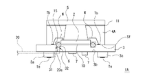
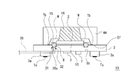
- FIG. 1 is a schematic longitudinal sectional view of a semiconductor device as a first embodiment according to the present technology
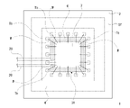
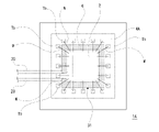
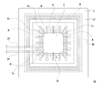
- FIG. 1 is a schematic plan view of a semiconductor device as a first embodiment according to the present technology
- FIG. It is a schematic longitudinal cross-sectional view of a semiconductor device as a modification of the first embodiment.
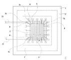
- FIG. 11 is a schematic plan view of a semiconductor device as a modified example of the first embodiment;
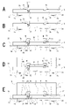
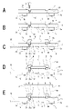
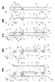
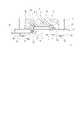
- FIG. 4 is an explanatory diagram of an example of a method for manufacturing a semiconductor device according to the first embodiment; It is explanatory drawing of the modification about a connection path
- 3 is a schematic longitudinal sectional view of a semiconductor device as a second embodiment
- FIG. FIG. 4 is a schematic plan view of a semiconductor device as a second embodiment;
- FIG. 10 is an explanatory diagram of an example of a method for manufacturing a semiconductor device as a second embodiment; It is a schematic vertical cross-sectional view of a semiconductor device as a third embodiment.
- FIG. 11 is a schematic plan view of a semiconductor device as a third embodiment;
- FIG. 11 is an explanatory diagram of an example of a method for manufacturing a semiconductor device as a third embodiment;
- FIG. 11 is a schematic longitudinal sectional view of a semiconductor device as a first example in the fourth embodiment;
- FIG. 11 is an explanatory diagram of an example of a method for manufacturing a semiconductor device as a first example in the fourth embodiment;
- FIG. 12 is a schematic longitudinal sectional view of a semiconductor device as a second example in the fourth embodiment;
- FIG. 11 is a schematic longitudinal sectional view of a semiconductor device as a third example in the fourth embodiment;
- First Embodiment> (1-1. Configuration example of a semiconductor device) (1-2. Examples of manufacturing methods for semiconductor devices) ⁇ 2.
- Second Embodiment> ⁇ 3.
- Third Embodiment> ⁇ 4.
- Fourth Embodiment> ⁇ 5.
- Variation> ⁇ 6.
- FIG. 1 is a schematic longitudinal sectional view of a semiconductor device 1
- FIG. 2 is a schematic plan view of the semiconductor device 1.
- FIG. The vertical direction here is a direction parallel to the thickness direction of the semiconductor chip 2 included in the semiconductor device 1 .
- the semiconductor device 1 includes a semiconductor chip 2 on which various electronic circuit components such as transistors are formed, and a circuit for enabling signal exchange between the semiconductor chip 2 and an external device (an external device of the semiconductor device 1).
- the wiring board section 3 can be rephrased as an interposer board.
- the semiconductor device 1 is configured as a solid-state imaging device (image sensor) such as a CCD (Charge Coupled Device) sensor or a CMOS (Complementary Metal Oxide Semiconductor) sensor.
- the semiconductor chip 2 is a semiconductor chip for receiving light for obtaining a captured image.
- a plurality of pixels having photoelectric conversion elements for performing photoelectric conversion are arranged two-dimensionally, and each pixel has a photoelectric conversion element.
- a pixel circuit is formed for reading out the accumulated charges.
- the semiconductor chip 2 has a plate-like outer shape with a rectangle.
- the semiconductor chip 2 is mounted on the wiring board portion 3 .
- the surface of the wiring board portion 3 on which the semiconductor chip 2 is mounted is referred to as a surface Sf
- the surface opposite to the surface Sf is referred to as a back surface Sb.
- the wiring board portion 3 is formed by alternately laminating wiring layers and insulating layers in which electrical wiring is formed in a predetermined pattern. Vias are formed in the insulating layer, and electrical wirings between wiring layers are electrically connected by the vias.
- a plurality of terminals Tb for electrical connection with the semiconductor chip 2 are formed on the surface Sf of the wiring board portion 3 .
- the semiconductor chip 2 is fixed to the surface Sf of the wiring substrate portion 3 by a chip adhesive 10 such as die bonding, and is connected to each terminal Tb formed on the surface Sf of the wiring substrate portion 3 via bonding wires W.
- Corresponding terminals are electrically connected. That is, the semiconductor chip 2 is electrically (and physically) connected to the wiring board portion 3 by wire bonding.
- a projecting portion 3a is formed on the rear surface Sb side of the wiring board portion 3 so as to project in the opposite direction to the side on which the semiconductor chip 2 is mounted.
- the projecting portion 3a is formed in a substantially rectangular frame shape in a plan view.
- a plurality of external connection terminals Te for electrical connection between the semiconductor device 1 and an external device are formed at the tip of the projecting portion 3a in the projecting direction. Signals can be exchanged between an external device and the semiconductor chip 2 via the external connection terminals Te.
- the electronic component 7 is mounted in a portion surrounded by the protruding portion 3a.
- FIG. 1 it is shown that a plurality of such “electronic components” are mounted, and each electronic component is given the same reference numeral "7".
- the electronic components may be components having the same function or components having different functions. In addition, they may have different shapes, sizes, and the like.
- the frame portion 4 protrudes from the wiring board portion 3 to the same side as the side on which the semiconductor chip 2 is mounted, and surrounds the side of the semiconductor chip. Specifically, the frame portion 4 in this example is provided on the surface Sf of the wiring board portion 3 on the outer periphery than the semiconductor chip 2 .
- the thickness of the frame portion 4, in other words, the total height of the frame portion 4 is made higher than the height of the bonding wires W (the height from the wiring board portion 3). Thereby, the frame portion 4 can protect components such as the semiconductor chip 2 and the bonding wires W mounted on the surface Sf side of the wiring substrate portion 3 from the sides.
- the lid portion 5 has a substantially rectangular plate shape and is arranged on the frame portion 4 so as to cover the entire space surrounded by the frame portion 4 above the surface Sf of the wiring board portion 3 .
- the lid portion 5 is adhered to the frame portion 4 with a lid portion adhesive 11 .
- the lid portion 5 seals the entire space surrounded by the frame portion 4 in order to protect the semiconductor chip 2 from the external environment such as water, humidity, and external force.
- the space surrounded by the frame portion 4 is filled with dry air or nitrogen and then sealed by the lid portion 5, or is evacuated and sealed by the lid portion 5. (i.e. vacuum sealed).
- the lid portion 5 is made of a transparent substrate such as glass.
- the heat exhaust member 6 is arranged between the bonding wire W and the wiring board portion 3 . That is, the heat exhaust member 6 is arranged at a position below the bonding wires W on the wiring board portion 3 .
- a heat pipe is used as the heat exhaust member 6 .
- the term "heat pipe” as used herein means a heat conductor in which a refrigerant (eg, liquid such as water) is sealed (eg, vacuum-sealed) in an airtight container and the inner wall of which has a capillary structure (wick).
- a metal pipe such as copper or aluminum having excellent thermal conductivity can be used.
- the heat exhaust member 6 is formed so as to surround the side surface of the semiconductor chip 2 substantially all around. In this manner, one end and the other end of the heat exhaust member 6 which substantially surrounds the side surface of the semiconductor chip 2 are connected via the connecting path 20, respectively.
- a heat radiation portion for cooling (liquefying) the refrigerant (which is vaporized by heating) in the heat pipe is formed. can be circulated (looped) through the heat exhaust member 6, the communication path 20, and the heat radiation portion.
- the connecting path 20 and the heat radiating section also have a heat pipe structure, and it can be said that the connecting path 20 and the heat radiating section constitute a part of the heat pipe.
- the inside is in a highly decompressed state, and the liquid as a refrigerant tends to evaporate easily.
- the liquid as a coolant becomes a vapor flow and moves to the unheated low temperature part (the above-mentioned heat dissipation part).
- the vapor that has moved touches the inner wall of the heat radiating part and returns to the liquid while transferring heat. This is called release of heat by latent heat of condensation.
- the refrigerant that has returned to a liquid state returns to its original location through the capillary structure, and when heated again, repeats the above-described evaporation, movement, and condensation, thereby transporting heat.
- Such a principle makes it possible to cool the target heat source.
- the heat exhaust member 6 is in contact with the side surface of the semiconductor chip 2 .
- the heat exhaust member 6 in this example is in contact with all four side surfaces of the semiconductor chip 2 .
- the heat exhaust member 6 is at least partially embedded in the groove 31 formed on the front surface Sf side of the wiring board portion 3 .
- the groove 31 is formed so as to encircle the semiconductor chip 2 in a plan view in the same manner as the heat dissipation member 6, so that the entire heat dissipation member 6 is embedded in the plan view.
- the depth of the groove 31 is formed shallower than the total height of the heat exhaust member 6 , so that part of the heat exhaust member 6 protrudes from the groove 31 , and part of the protruding portion of the heat exhaust member 6 extends from the semiconductor chip 2 . It is possible to touch the side of
- the heat exhaust member 6 By embedding at least part of the heat exhaust member 6 in the groove 31 , the heat exhaust member 6 with a larger cross-sectional area can be used in the limited space under the bonding wire W.
- the clearance in the height direction from the bonding wires W to the wiring substrate portion 3 is about 120 ⁇ m to 150 ⁇ m.
- the current thickness of the heat pipe is, for example, 150 ⁇ m or more. Therefore, at present, it is difficult to dispose the heat pipe in the space below the bonding wire W without processing the wiring substrate portion 3, and it is effective to provide the groove 31 as described above.
- the heat exhaust member 6 is adhered to the side surface of the semiconductor chip 2 with a thermally conductive resin 15 .
- a thermal conductive resin 15 it is desirable to use, for example, a thermosetting resin having a relatively high thermal conductivity.
- a resin paste for die bonding, a resin paste to which silver paste is added, and the like can be given.
- the ATROX (registered trademark) D800HT series manufactured by Techno Alpha can be used.
- the heat exhaust member 6 When a heat pipe is used as the heat exhaust member 6 as in this example, when the cross-sectional shape of the heat exhaust member 6 is a shape other than a rectangle, the heat exhaust member 6 is evenly attached to the side surface of the semiconductor chip 2. is difficult. Therefore, by bonding the heat exhaust member 6 to the side surface of the semiconductor chip 2 using the heat conductive resin 15, the degree of thermal adhesion of the heat exhaust member 6 to the semiconductor chip 2 is enhanced.
- a material having adhesiveness in order to increase the degree of thermal adhesion of the heat exhaust member 6 to the semiconductor chip 2 .
- a heat dissipation paste such as TIM (Thermal Interface Materials) manufactured by Cosmo Oil Lubricants Co., Ltd. so as to fill the gap between the heat dissipation member 6 and the semiconductor chip 2 .
- the connecting path 20 from the heat exhausting member 6 to the above-described heat radiating portion is formed on the rear surface Sb side of the wiring board portion 3 .
- a part 20a (see FIG. 1) of the connection path 20 in this case is arranged in a groove 32 penetrating the wiring board portion 3 in the thickness direction, and is partially embedded in the groove 31. It is connected to the end of the heat exhaust member 6 that is present.
- a part 20a of one connecting path 20 is connected to one end of the heat exhausting member 6, and a part 20a of the other connecting path 20 is connected to the other end of the heat exhausting member 6. connected to the department.
- the connecting path 20 By forming the connecting path 20 on the back surface Sb side of the wiring board portion 3 as described above, when the molded product as the frame portion 4 is attached to the wiring board portion 3, the frame portion 4 side can be processed (the connecting path 20 Formation of groove 32 for passage) can be made unnecessary.
- FIG. 3 and 4 are diagrams for explaining the configuration of a semiconductor device 1' as a modified example of the first embodiment.
- FIG. 3 is a schematic longitudinal sectional view of the semiconductor device 1'
- FIG. ' is a schematic plan view of FIG.
- the same reference numerals will be given to the same parts as those already explained, and the explanation will be omitted.
- the semiconductor device 1 ′ differs from the semiconductor device 1 in the route layout of the heat exhaust member 6 .
- a portion of the heat exhaust member 6 is arranged at a position below the semiconductor chip 2 inside the wiring board portion 3 .
- the heat exhaust member 6 is formed to have a plurality of folded portions below the semiconductor chip 2 .
- the folded portion referred to here means a portion accompanied by folding in the surface direction of the wiring board portion 3 .
- the portion of the heat exhausting member 6 other than the above portion is arranged along the side surface of the semiconductor chip 2 and partially contacts the side surface of the semiconductor chip 2 as in the case of the semiconductor device 1. It is made like this.
- a groove 31 ′ is formed in the wiring board portion 3 instead of the groove 31 .
- the portion positioned below the semiconductor chip 2 is formed with a depth such that the heat exhausting member 6 is buried in the groove 31 ′ (that is, the entire portion is buried), and the portion along the side surface of the semiconductor chip 2 is formed. is formed to a depth such that a portion of the heat exhaust member 6 protrudes from the groove 31' (a depth at which a portion of the heat exhaust member 6 can be in contact with the side surface of the semiconductor chip 2).
- one end of the heat exhaust member 6 is connected to one communication path 20, and the other end of the heat exhaust member 6 is connected to the other communication path 20, as in the case of the semiconductor device 1.
- heat exhaust member 6 By arranging part of the heat exhaust member 6 below the semiconductor chip 2 as described above, heat can be exhausted from below the semiconductor chip 2 as well, and the cooling efficiency of the semiconductor chip 2 can be improved. can.
- the heat exhaust member 6 by forming the heat exhaust member 6 by folding it under the semiconductor chip 2, the heat exhaust efficiency from the semiconductor chip 2 to the heat exhaust member 6 can be improved, and in this respect also, the cooling efficiency can be improved. can.
- a groove 31 is formed in the wiring board portion 3 by countersinking with a router bit or the like (see FIG. 5A).
- the grooves 31 are formed on the surface Sf side of the wiring board portion 3 at positions surrounding the mounting position of the semiconductor chip 2 .
- a groove 32 for arranging a portion 20a of the connecting path 20 is also formed in the wiring board portion 3.
- the groove 31' described above is formed instead of the groove 31 in the process of FIG. 5A.
- the semiconductor chip 2 is mounted on the front surface Sf side of the wiring substrate portion 3 (see FIG. 5B).
- the semiconductor chip 2 is adhered to a predetermined position on the inner peripheral side of the groove 31 on the surface Sf side of the wiring board portion 3 with the chip adhesive 10 .
- a thermally conductive resin 15 such as a thermosetting resin is applied to the heat exhaust member 6 arranged in the groove 31, and the thermally conductive resin 15 is thermally cured.
- the terminals formed on the semiconductor chip 2 and the terminals Tb formed on the front surface Sf of the wiring substrate portion 3 are connected by bonding wires W, and the semiconductor chip 2 is wire-bonded to the wiring substrate portion 3 .
- the step of forming the connecting path 20 is performed. At this time, the part 20 a of the connecting path 20 is inserted into the groove 32 .
- the frame portion 4 as a molded product made of mold resin, for example, is attached to the surface Sf side of the wiring substrate portion 3 (see FIG. 5D).
- the lid portion 5 as a transparent substrate is adhered with the lid portion adhesive 11 applied on the frame portion 4, thereby sealing the space surrounded by the frame portion 4 on the surface Sf of the wiring substrate portion 3. (See FIG. 5E).
- the semiconductor device 1 described with reference to FIGS. 1 and 2 is produced.
- the connecting path 20 is arranged on the back surface Sb side of the wiring board portion 3.
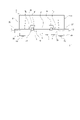
- FIG. 6 shows an example in which a groove for burying the connecting path 20 is formed on the surface Sf side of the wiring board portion 3, and the heat exhausting member serving as the connecting path 20 is arranged in the groove.
- the frame portion 4 when a molded product is used as the frame portion 4, depending on the depth of the groove formed on the surface Sf for the communication path 20, the communication path 20 cannot be accommodated in the groove, and the frame portion 4 has A groove may have to be formed for passage of the communication path 20 .
- transfer molding a molding method in which a mold is arranged and resin is poured into it
- the frame portion 4 A step of forming a groove for the can be omitted.
- connecting path 20 is formed on the surface Sf side of the wiring board portion 3 as shown in FIG. can be used.
- FIG. 7 and 8 are a schematic longitudinal sectional view and a schematic plan view of the semiconductor device 1A, respectively.
- a semiconductor device 1A of the second embodiment differs from the semiconductor device 1 of the first embodiment in that a frame portion 4A is provided instead of the frame portion 4.
- FIG. The frame portion 4A differs from the frame portion 4 in that it is formed at a position covering the bonding wires W. As shown in FIG. In this example, the frame portion 4A is formed so as to cover the bonding wire W entirely. As a result, the inner peripheral portion of the frame portion 4A extends to the outer edge portion of the semiconductor chip 2. As shown in FIG.
- the size of the semiconductor device 1 increases accordingly. Since there is no gap between the semiconductor chip 2 and the frame portion 4A, the size of the semiconductor device 1A can be reduced.
- the frame portion 4A is formed on the wiring substrate portion 3 by transfer molding, for example, instead of attaching a molded product to the wiring substrate portion 3. As shown in FIG. When a molded product is used as the frame portion 4A, it is desirable to form grooves for accommodating the bonding wires W and the outer edge portion of the semiconductor chip 2.
- FIG. 1 When a molded product is used as the frame portion 4A, it is desirable to form grooves for accommodating the bonding wires W and the outer edge portion of the semiconductor chip 2.
- FIG. 9 is an explanatory diagram of an example of a method for manufacturing the semiconductor device 1A as the second embodiment.
- the steps shown in FIGS. 9A to 9C are the same as those explained in FIGS. 5A to 5C, so repeated explanations are avoided.
- the step of forming the frame portion 4A shown in FIG. 9D is performed after the step of FIG. 9C (wire bonding and formation of the connecting path 20).
- the frame portion 4A is formed by transfer molding.
- the space surrounded by the frame portion 4A is sealed by adhering the lid portion 5 as a transparent substrate with the lid portion adhesive 11 applied on the frame portion 4A as shown in FIG. 9E. stop.
- the connecting path 20 is formed on the back surface Sb side of the wiring substrate portion 3 as in the semiconductor device 1
- the connecting path 20 is formed as in the semiconductor device 1'' (FIG. 6).
- it may be formed on the surface Sf side of the wiring board portion 3 .
- a configuration in which a portion of the heat exhaust member 6 is arranged below the semiconductor chip 2 as in the semiconductor device 1' (FIGS. 3 and 4) can be employed.
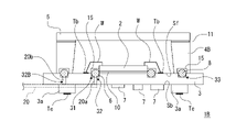
- Third Embodiment> 10 and 11 are a schematic longitudinal sectional view and a schematic plan view, respectively, of a semiconductor device 1B as a third embodiment.
- a heat exhausting member different from the heat exhausting member 6 provided on the side surface of the semiconductor chip 2 is arranged in a frame portion constituting the side wall portion of the semiconductor device 1B.
- In-frame heat exhaust member 8 in the figure Since the wiring board portion 3 also functions as a heat exhaust path for heat generated in the semiconductor chip 2 , the heat from the semiconductor chip 2 can also be exhausted by the in-frame heat exhaust member 8 .
- the semiconductor device 1B differs from the semiconductor device 1 in that a frame portion 4B is provided in place of the frame portion 4 and an in-frame heat exhaust member 8 is provided in the frame portion 4B.
- the in-frame heat exhaust member 8 is configured by, for example, a heat pipe, like the heat exhaust member 6 .
- the wiring board portion 3 is formed with a groove 33 for burying a portion of the in-frame heat exhaust member 8 in the region covered by the frame portion 4B.
- the in-frame heat exhaust member 8 is formed so as to encircle the side of the semiconductor chip 2 in the same manner as the heat exhaust member 6, and the groove 33 is formed in the same manner. is formed so as to encircle the sides of the semiconductor chip 2 substantially.
- the heat-dissipating member 8 in the frame is adhered to the wiring board portion 3 by applying a heat-conducting resin 15 from above. As a result, the degree of thermal adhesion to the wiring board portion 3 can be enhanced.
- the frame portion 4B is formed so as to cover the in-frame heat exhaust member 8 adhered to the wiring board portion 3 in this way.
- the frame portion 4B can also be formed by transfer molding, for example, in the same manner as the frame portion 4A.
- the communication path 20 is shared by the heat exhaust member 6 and the in-frame heat exhaust member 8 .
- one end of the in-frame heat exhaust member 8 is connected to a connecting path 20 connected to one end of the heat exhaust member 6
- the other end of the heat exhaust member 6 is connected to the connecting path 20 .
- the other end portion of the in-frame heat exhaust member 8 is connected to a communication path 20 connected to the portion.
- connection path 20 is formed on the back surface Sb side of the wiring board portion 3 as in the case of the semiconductor device 1 .
- the wiring board portion 3 in this case has grooves 32 for connecting the heat exhausting member 6 and the communication path 20, as well as grooves 32 for connecting the in-frame heat exhausting member 8 and the communication path 20 in the thickness direction.
- Two grooves 32B are formed (one for one end and one for the other end).
- a portion 20b (a portion different from the portion 20a described above) of the connecting path 20 is inserted into the groove 32B to be connected to the in-frame heat exhaust member 8 .
- the in-frame heat exhaust member 8 and the heat exhaust member 6 share the communication path 20, in other words, share the heat radiating section. It is also possible to adopt a configuration in which the cooling circuit passing through the heat member 8 is formed as a different loop circuit, and the heat exhaust member 6 and the in-frame heat exhaust member 8 are connected to different heat radiating portions.
- the grooves 31 and 32 as well as the grooves 33 and 32B are formed in the wiring board portion 3 by, for example, counter boring using a router bit or the like (see FIG. 12A). Then, in the same manner as the step of FIG. 5B described above, the step of bonding the semiconductor chip 2 to the wiring board portion 3 is performed (see FIG. 12B).
- the heat exhaust member 6 is arranged in the groove 31, and the in-frame heat exhaust member 8 is arranged in the groove 33, and heat is conducted to the heat exhaust member 6 and the in-frame heat exhaust member 8.
- the thermal conductive resin 15 is thermally cured.
- the terminal of the semiconductor chip 2 and the terminal Tb are wire-bonded with the bonding wire W, and the connecting path 20 is formed. That is, in this case, the portion 20a inserted through the groove 32 is connected to the heat exhausting member 6, and the portion 20b inserted through the groove 32B is connected to the in-frame heat exhausting member 8, respectively.
- the members 8 are each communicated with the communication path 20 .
- the frame portion 4B covering the in-frame heat exhaust member 8 is formed on the surface Sf side of the wiring board portion 3, and in the step shown in FIG.
- the space surrounded by the frame portion 4B is sealed by adhering the lid portion 5 as a transparent substrate with the portion adhesive 11. As shown in FIG.
- the heat exhausting member 6 may be omitted and only the in-frame heat exhausting member 8 may be provided.
- FIG. 13 is a schematic longitudinal sectional view of a semiconductor device 1C as a first example in the fourth embodiment.
- the transparent substrate as the lid portion 5 is omitted, and the space surrounded by the frame portion is filled with the transparent resin 16 to seal.
- a semiconductor device 1C as a first example is obtained by applying a cavityless structure to the semiconductor device 1 of the first embodiment, and compared with the semiconductor device 1, the lid portion 5 (and the lid portion adhesive 11 ) is omitted, the space surrounded by the frame portion 4 is filled with a transparent resin 16 .
- the semiconductor chip 2 is covered with the transparent resin 16 in the space surrounded by the frame portion 4 .
- the space surrounded by the frame portion 4 is evacuated or filled with a predetermined gas such as nitrogen.
- the thermal conductivity in the area surrounded by the frame portion 4 can be increased more by adopting a cavityless structure in which the transparent resin 16 is filled than in that case. Therefore, heat is efficiently conducted from the upper surface side of the semiconductor chip 2 to the transparent resin 16 , so that heat is efficiently conducted from the transparent resin 16 to the heat exhaust member 6 . It is possible to improve the cooling efficiency.
- FIG. 13 shows an example in which the connection path 20 is formed on the back surface Sb side of the wiring board portion 3 as an example of the cavityless structure. It can be formed on the Sf side. Also, when adopting a cavityless structure, a structure in which a portion of the heat exhausting member 6 is arranged below the semiconductor chip 2 as illustrated in FIGS. 3 and 4 can be adopted.
- FIG. 14 is an explanatory diagram of an example of a method for manufacturing the semiconductor device 1C.
- the steps of FIGS. 14A to 14D are the same as the steps described in FIGS. 5A to 5D, so redundant description is avoided.
- the space surrounded by the frame portion 4 is filled with the transparent resin 16 in the process of FIG. 14E.
- FIG. 15 is a schematic longitudinal sectional view of a semiconductor device 1D as a second example of the fourth embodiment
- FIG. 16 is a schematic longitudinal sectional view of a semiconductor device 1E as a third example of the fourth embodiment.
- a semiconductor device 1D as a second example is obtained by applying a cavityless structure to the semiconductor device 1A (FIGS. 7 and 8) as the second embodiment
- a semiconductor device 1E as a third example is the semiconductor device 1E as the third embodiment.
- a cavityless structure is applied to the semiconductor device 1B (FIGS. 10 and 11).
- 9E and 12E are replaced with a step of filling the space surrounded by the frame portion 4A with the transparent resin 16 and a step of filling the space surrounded by the frame portion 4A with the frame portion 4B.
- a step of filling the space surrounded by with the transparent resin 16 may be performed.
- a cooling circuit using a heat pipe is given as an example of a cooling circuit for heat generated in the semiconductor chip 2, but the cooling circuit using a heat pipe is limited to the illustrated loop type. not.
- a cooling circuit in which a portion of a rod-shaped heat pipe is arranged along one of the side surfaces of the semiconductor chip 2 may be used.
- the heat exhaust member 6 (and the in-frame heat exhaust member 8) is a heat pipe. It is possible to use members other than heat pipes, such as tubular members through which coolant is transferred.
- the frame portion which is the side wall portion of the semiconductor device, is separate from the wiring substrate portion, but the frame portion may be integrated with the wiring substrate portion.
- this technology is applied to a semiconductor device as a solid-state image pickup device, but this technology can be applied to an array of light-emitting devices such as VCSELs (Vertical Cavity Surface Emitting Lasers).
- VCSELs Vertical Cavity Surface Emitting Lasers
- Widely suitable for semiconductor devices other than solid-state imaging devices such as a semiconductor device as a light-emitting device arranged in a vertical direction, a semiconductor device as a distance measurement sensor in which pixels that receive light for distance measurement are arranged two-dimensionally, etc. applicable to
- the semiconductor device (same 1, 1′, 1′′, 1A, 1B, 1C, 1D, 1E) of the embodiment includes a semiconductor chip (same 2) and a semiconductor chip mounted thereon.
- a wiring board portion (3) having external connection terminals (Te) for electrical connection with the outside on the back surface side, which is the surface opposite to the front surface, which is the surface on the side of the printed wiring board;
- the semiconductor chip is connected to terminals formed on the surface side of the wiring substrate portion by bonding wires (W) and wire-bonded to the wiring substrate portion, and a heat dissipation member ( 6) is arranged.
- the heat exhaust member is arranged in the vicinity of the semiconductor chip serving as a heat source.
- the semiconductor device can be cooled by a heat exhaust member arranged in the dead space below the bonding wires. Since the semiconductor device can be cooled by the heat exhaust member arranged in the dead space, it is possible to prevent the semiconductor device from becoming large due to cooling.
- the heat exhaust member is in contact with the side surface of the semiconductor chip. This improves the efficiency of heat conduction from the semiconductor chip to the heat exhaust member. Therefore, it is possible to improve the cooling efficiency.
- the heat exhaust member is configured by a heat pipe. Since the heat pipe is capable of circulating the coolant by capillary action, a drive unit for circulating the coolant is not required, which simplifies the cooling structure and reduces the number of parts required for cooling. Cost reduction of the semiconductor device can be achieved.
- the frame portion (4A of the same) protrudes from the wiring substrate portion to the same side as the side on which the semiconductor chip is mounted and encloses the side of the semiconductor chip. covers the bonding wire.
- the inner periphery of the frame extends to the outer edge of the semiconductor chip. Therefore, the size of the semiconductor device can be reduced more than in the case of a package in which the inner peripheral edge of the frame portion is located on the outer peripheral side of the semiconductor chip.
- the bonding wires are covered by the frame portion, so that the effect of reducing the flare caused by the bonding wires can be obtained.
- the frame portion protrudes from the wiring substrate portion to the same side as the side on which the semiconductor chip is mounted, is provided on the outer periphery of the semiconductor chip, and surrounds the side of the semiconductor chip. (4B), and an in-frame heat exhaust member (8), which is a different heat exhaust member from the heat exhaust member, is arranged in the frame portion. Since the wiring board portion also functions as a heat exhaust path for heat generated in the semiconductor chip, the heat from the semiconductor chip can also be exhausted by the in-frame heat exhausting member (via the wiring substrate portion ⁇ frame portion). becomes possible. Therefore, it is possible to improve the cooling efficiency. Moreover, since the inside of the frame portion is also a dead space, the dead space can be effectively utilized as a heat exhaust path.
- At least part of the heat exhausting member is embedded in the grooves (31, 31') formed on the surface side of the wiring board portion.
- the heat exhaust member is adhered to the side surface of the semiconductor chip with a thermally conductive resin (same 15).
- a thermally conductive resin for example, when a heat pipe is used as the heat exhaust member and the cross-sectional shape of the heat exhaust member is not rectangular, it is difficult to evenly attach the heat exhaust member to the side surface of the semiconductor chip. Therefore, by bonding the heat exhausting member to the side surface of the semiconductor chip using a heat conductive resin, the degree of thermal adhesion of the heat exhausting member to the semiconductor chip is increased. As a result, the heat from the semiconductor chip can be efficiently led to the heat exhaust member through the heat conductive resin, and the cooling efficiency can be improved.
- thermosetting resin can be selected as the heat conductive resin, so the efficiency of the bonding process of the heat exhausting member can be improved, and the position of the heat exhausting member can be fixed by bonding, resulting in cooling performance. stability can be improved.
- the semiconductor chip is formed in a substantially rectangular plate shape, and the heat exhaust member is in contact with all four side surfaces of the semiconductor chip. This allows the heat generated in the semiconductor chip to be led to the heat exhaust member from all four side surfaces of the semiconductor chip. Therefore, it is possible to improve the cooling efficiency.
- a connection path (same 20) from the heat exhausting member to the heat radiating portion is formed on the surface side of the wiring board portion.
- the communication path from the heat exhaust member to the heat radiating portion is formed on the back surface side of the wiring substrate portion.
- the frame portion protrudes from the wiring substrate portion to the same side as the side on which the semiconductor chip is mounted and encloses the side of the semiconductor chip; and a transparent resin (same 16) filled in the enclosed space. That is, it adopts a so-called cavityless structure (cavityless structure) in which the region surrounded by the frame portion is not sealed from the upper side of the frame portion with a lid portion such as glass. In the space, the semiconductor chip is covered with transparent resin.
- a cavity structure in which a space surrounded by a frame is sealed by a lid is adopted, the space surrounded by the frame is either evacuated or filled with a predetermined gas such as nitrogen.
- the cavityless structure filled with transparent resin can increase the thermal conductivity in the region surrounded by the frame portion. Therefore, heat is efficiently conducted from the upper surface side of the semiconductor chip to the transparent resin, whereby heat can be efficiently conducted from the transparent resin to the heat exhaust member, resulting in cooling efficiency. can be improved. Moreover, since it has a cavityless structure, it is possible to eliminate the need for a sealing process using a lid, and in this respect, it is possible to reduce the manufacturing cost of the semiconductor device.
- the semiconductor device of the embodiment is a semiconductor device as a solid-state imaging device. Thereby, it is possible to improve the cooling efficiency of the semiconductor device as a solid-state imaging device.
- a semiconductor chip is mounted, and electrical connection with the outside is provided on the back surface side, which is the surface opposite to the surface on which the semiconductor chip is mounted. and a semiconductor chip is wire-bonded to the wiring substrate portion by connecting the semiconductor chip to the terminals formed on the surface side of the wiring substrate portion by bonding wires.
- the device manufacturing method includes at least a step of disposing a heat exhaust member at a position between the bonding wire and the wiring board portion.
- the present technology can also adopt the following configuration.
- a semiconductor chip A wiring board on which the semiconductor chip is mounted, and on which an external connection terminal for electrical connection with the outside is formed on the back surface, which is the surface opposite to the surface on which the semiconductor chip is mounted. and the semiconductor chip is connected to a terminal formed on the front surface side of the wiring substrate portion by a bonding wire and wire-bonded to the wiring substrate portion; A semiconductor device, wherein a heat exhausting member is arranged between the bonding wire and the wiring board portion.
- the heat exhaust member is a heat pipe.
- a method for manufacturing a semiconductor device in which the semiconductor chip is connected to a terminal formed on the front surface side of the wiring substrate portion by a bonding wire and wire-bonded to the wiring substrate portion A method of manufacturing a semiconductor device, comprising at least the step of arranging a heat exhaust member at a position between the bonding wire and the wiring board portion.
Landscapes
- Cooling Or The Like Of Semiconductors Or Solid State Devices (AREA)
- Chemical & Material Sciences (AREA)
- Engineering & Computer Science (AREA)
- Materials Engineering (AREA)
Abstract
Description
上記の配線基板部は、半導体チップと外部装置との間で信号のやりとりを可能とするための配線が形成された部分である。例えば、半導体チップは、この配線基板部の表面、すなわち半導体チップが実装される側の面に形成された端子に対してワイヤボンディングされて配線基板部と電気的に接続される。
半導体チップの発熱量が増大することによっては、配線基板部や半導体チップ自体に変形が生じる等して、所期の機能を満たすことができなくなる虞がある。そのため、半導体装置に冷却のための構成を設けるということが行われている。
排熱部材とは、半導体チップで生じた熱についての冷却を行うための排熱経路の少なくとも一部を形成する部材を意味する。上記構成によれば、熱源となる半導体チップの近傍に排熱部材が配置される。そして、この場合の半導体装置の冷却は、ボンディングワイヤ下としてのデッドスペースに配置した排熱部材により行うことが可能とされる。
これにより、半導体チップから排熱部材への熱伝導効率の向上が図られる。
ここで言うヒートパイプとは、密閉容器内に冷媒(例えば水等の液体)が密封され、内壁に毛細管構造(ウイック)を備えた熱伝導体を意味する。
これにより、フレーム部の内周部は半導体チップの外縁部まで及ぶものとなる。
配線基板部は半導体チップで生じた熱についての排熱経路としても機能するため、フレーム内排熱部材によっても半導体チップからの熱を(配線基板部→フレーム部を経由して)排熱することが可能となる。
上記のように配線基板部に形成した溝内に排熱部材の少なくとも一部を埋設することで、ボンディングワイヤ下という限られたスペース内において、より断面積の大きな排熱部材を使用可能となる。
例えば排熱部材としてヒートパイプを用いる場合等、排熱部材の断面形状が矩形以外の形状等とされる場合には、排熱部材を半導体チップ側面に満遍なく密着させることは困難である。そこで、排熱部材を熱伝導樹脂を用いて半導体チップ側面に接着させることで、排熱部材の半導体チップに対する熱的な密着度を高めるようにする。
これにより、半導体チップで生じた熱を半導体チップの四つの側面の全てから排熱部材に導くことが可能とされる。
これにより、排熱部材と連絡経路とを連接させるにあたり配線基板部に対する穴開け加工を不要とすることが可能となる。
これにより、フレーム部として成形品を配線基板部に貼り付ける場合に、フレーム部側に対する加工(連絡経路を通すための溝の形成)を不要とすることが可能となる。
すなわち、フレーム部で囲われた領域をフレーム部の上側からガラス等の蓋部によって封止しない、いわゆるキャビレス構造(キャビティレス構造)を採るものであり、この場合には、フレーム部で囲われた空間内において、半導体チップが透明樹脂で覆われるものとなる。
これにより、固体撮像素子としての半導体装置について、冷却効率の向上が図られる。
このような製造方法により、上記した本技術に係る半導体装置を製造することが可能となる。
<1.第一実施形態>
(1-1.半導体装置の構成例)
(1-2.半導体装置の製造方法例)
<2.第二実施形態>
<3.第三実施形態>
<4.第四実施形態>
<5.変形例>
<6.実施形態のまとめ>
<7.本技術>
(1-1.半導体装置の構成例)
図1及び図2を参照して第一実施形態としての半導体装置1について説明する。
図1は、半導体装置1の概略縦断面図、図2は半導体装置1の概略平面図である。なお、ここでの縦方向とは、半導体装置1が備える半導体チップ2の厚み方向に平行な方向である。
ここで、配線基板部3は、インターポーザ基板と換言できるものである。
半導体チップ2は、本例では撮像画像を得るための受光用の半導体チップとされ、光電変換を行う光電変換素子を有する画素が二次元に複数配列されていると共に、画素ごとに光電変換素子の蓄積電荷を読み出すための画素回路が形成されている。
半導体チップ2は、矩形による板状の外形形状を有する。
半導体チップ2は、配線基板部3の表面Sfにダイボンド等のチップ接着剤10によって固定されると共に、配線基板部3の表面Sfに形成された各端子Tbに対し、ボンディングワイヤWを介してそれぞれ対応する端子が電気的に接続されている。すなわち、半導体チップ2は、配線基板部3に対してワイヤボンディングにより電気的(及び物理的)に接続されている。
突出部3aの突出方向における先端部には、半導体装置1の外部装置との間で電気的接続を行うための外部接続端子Teが複数形成されている。この外部接続端子Teを介して、外部装置と半導体チップ2との間で信号のやりとりを行うことが可能とされる。
フレーム部4の厚さ、換言すればフレーム部4の全高は、ボンディングワイヤWの高さ(配線基板部3からの高さ)よりも高くされている。これによりフレーム部4は、配線基板部3の表面Sf側に実装された半導体チップ2やボンディングワイヤWといった部品を側方から保護することが可能とされている。
この蓋部5によっては、半導体チップ2を水、湿度、外力など外部環境から保護するため、フレーム部4で囲われた空間全体が密閉されている。具体的に本例では、フレーム部4で囲われた空間は、ドライエアや窒素が充填された上で蓋部5により封止されるか、或いは真空に引かれて蓋部5により封止される(つまり真空封止される)。
固体撮像素子である本例の半導体装置1においては、蓋部5は例えばガラス等の透明基板で構成されている。
本例において、排熱部材6にはヒートパイプが用いられる。ここで言うヒートパイプとは、密閉容器内に冷媒(例えば水等の液体)が密封(例えば、真空密封)され、内壁に毛細管構造(ウイック)を備えた熱伝導体を意味する。
ヒートパイプとしては、熱伝導性に優れる例えば銅製やアルミ製等の金属製パイプを用いることができる。
溝31は、平面視において排熱部材6と同様に半導体チップ2の周囲を略一周囲うように形成されており、これにより平面視において排熱部材6全体を埋設するようにされている。
溝31の深さは、排熱部材6の全高よりも浅く形成され、これにより排熱部材6の一部が溝31から突出し、排熱部材6の該突出した部分の一部が半導体チップ2の側面に接することが可能とされている。
例えば、具体的な数値の一例として、ボンディングワイヤWから配線基板部3までの高さ方向のクリアランスは120μmから150μm程度である。一方で、排熱部材6としてヒートパイプを用いた場合、現状におけるヒートパイプの厚みは例えば150μm以上となる。このため現状では、ヒートパイプをボンディングワイヤWの下方スペースに配線基板部3の加工なしに配置することは困難であり、上記のような溝31を設けることが有効となる。
熱伝導樹脂15としては、例えば熱硬化樹脂で比較的熱伝導率の高い樹脂を用いることが望ましい。一例としては、例えばダイボンド用の樹脂ペーストや、銀ペーストが添加された樹脂ペースト等を挙げることができる。具体的には、テクノアルファ社製のATROX(登録商標)D800HTシリーズ等を挙げることができる。
具体的に、この場合の連絡経路20の一部20a(図1参照)は、配線基板部3の厚み方向を貫通する溝32内に配置されており、溝31内に一部が埋設されている排熱部材6の端部と連接されている。本例では、連絡経路20は二本あり、一方の連絡経路20の一部20aは排熱部材6の一端部に連接され、他方の連絡経路20の一部20aは排熱部材6の他端部に連接されている。
なお、以下の説明において、既に説明済みとなった部分と同様となる部分については同一符号を付して説明を省略する。
半導体装置1’においては、排熱部材6の一部が配線基板部3内部における半導体チップ2の下方となる位置に配置されている。具体的に本例では、排熱部材6は、半導体チップ2の下方において複数の折り返し部を有するように形成されている。ここで言う折り返し部とは、配線基板部3の面方向における折り返しを伴う部分を意味する。
また、本例において、排熱部材6の上記一部を除いた部分は、半導体装置1の場合と同様、半導体チップ2の側面に沿うように配置され、半導体チップ2の側面と一部が接するようにされている。
この場合も排熱部材6の一端部が一方の連絡経路20と連接され、排熱部材6の他端部が他方の連絡経路20と連接される点は半導体装置1の場合と同様である。
また、半導体チップ2の下方において、排熱部材6を折り返して形成することで、半導体チップ2から排熱部材6への排熱効率を高めることができ、この点においても冷却効率向上を図ることができる。
図5を参照し、半導体装置1の製造方法例について説明する。
先ず、ルータービット等による座繰り加工により、配線基板部3に対して溝31を形成する(図5A参照)。先の説明から理解されるように、溝31は、配線基板部3の表面Sf側において、半導体チップ2の搭載位置の周囲となる位置に形成する。
また、図5Aに示す工程では、配線基板部3に対して連絡経路20の一部20aを配置するための溝32の形成も行う。
なお、図3及び図4で説明した半導体装置1’の製造においては、図5Aの工程において溝31に代えて前述した溝31’を形成する。
また、本例では、このワイヤボンディング後、連絡経路20の形成工程を行う。このとき、連絡経路20の一部20aを溝32内に挿通させる。この一部20aは、排熱部材6の一端部、他端部に対応した二つが存在するが、本例において、排熱部材6の一端部と一方の一部20aとの接続、排熱部材6の他端部と他方の一部20aとの接続は、それぞれヒートパイプ構造が維持されるようにして行う。
その上で、フレーム部4上に塗布した蓋部接着剤11により透明基板としての蓋部5を接着することで、配線基板部3の表面Sf上におけるフレーム部4で囲われた空間を封止する(図5E参照)。
これにより、図1や図2で説明した半導体装置1が生成される。
図6では、配線基板部3の表面Sf側に連絡経路20埋設用の溝を形成し、該溝に連絡経路20となる排熱部材を配置する例を示している。
しかしながら、フレーム部4として成形品を用いるのではなく、フレーム部4をトランスファモールド(金型を配置しそこに樹脂を流し込む成形方式)により配線基板部3上に形成する場合には、フレーム部4に対する溝の形成工程は不要とすることができる。
続いて、図7及び図8を参照して第二実施形態としての半導体装置1Aについて説明する。図7、図8は、それぞれ半導体装置1Aの概略縦断面図、概略平面図である。
第二実施形態の半導体装置1Aは、第一実施形態の半導体装置1と比較して、フレーム部4に代えてフレーム部4Aが設けられた点が異なる。
フレーム部4Aは、ボンディングワイヤWを覆う位置に形成された点がフレーム部4と異なる。本例では、フレーム部4Aは、ボンディングワイヤWの全体を覆うように形成されている。これにより、フレーム部4Aの内周部は半導体チップ2の外縁部まで及ぶものとなる。
第一実施形態の半導体装置1では、半導体チップ2とフレーム部4との間に間隙が生じているため、その分、半導体装置1のサイズが大きくなるが、第二実施形態の半導体装置1Aでは、半導体チップ2とフレーム部4Aとの間に間隙が生じないため、半導体装置1Aの小型化を図ることができる。
なお、フレーム部4Aとして成形品を用いる場合には、ボンディングワイヤWや半導体チップ2の外縁部を収容するための溝を形成しておくことが望ましい。
図9Aから図9Cに示す工程については、図5Aから図5Cで説明したものと同様となることから重複説明は避ける。
この場合は、図9Cの工程(ワイヤボンディング及び連絡経路20の形成)の後、図9Dに示すフレーム部4Aの形成工程を行う。例えば本例では、フレーム部4Aの形成は、トランスファモールドにより行う。
また、第二実施形態においても、半導体装置1’(図3、図4)のように排熱部材6の一部を半導体チップ2の下方に配置する構成を採ることもできる。
図10及び図11は、それぞれ第三実施形態としての半導体装置1Bの概略縦断面図、概略平面図である。
第三実施形態としての半導体装置1Bは、半導体チップ2側面に対して設けられた排熱部材6とは別の排熱部材を、半導体装置1Bの側壁部を構成するフレーム部内に配置したものである(図中、フレーム内排熱部材8)。
配線基板部3は、半導体チップ2で生じた熱についての排熱経路としても機能するため、フレーム内排熱部材8によっても半導体チップ2からの熱を排熱することが可能となる。
この場合、配線基板部3には、フレーム部4Bによって覆われる領域内にフレーム内排熱部材8の一部を埋設するための溝33が形成される。図11に例示するように、本例では、フレーム内排熱部材8としても、排熱部材6と同様に半導体チップ2の側方を略一周するように形成されており、溝33としても同様に半導体チップ2の側方を略一周するように形成されている。
フレーム部4Bについても、先のフレーム部4Aと同様に、例えばトランスファモールドにより形成することができる。或いは、フレーム内排熱部材8を収容可能な溝を形成した成形品を配線基板部3に貼り合わせることも可能である。
先ず、配線基板部3に対し、例えばルータービット等による座繰り加工により溝31及び溝32と共に溝33及び溝32Bを形成する(図12A参照)。そして、先に説明した図5Bの工程と同様に、配線基板部3に対する半導体チップ2の接着工程を行う(図12B参照)。
第四実施形態は、いわゆるキャビレス構造(キャビティレス構造)に係る実施形態である。
図13は、第四実施形態における第一例としての半導体装置1Cの概略縦断面図である。キャビレス構造は、蓋部5としての透明基板を省略し、フレーム部で囲われた空間を透明樹脂16の充填により封止するものである。
具体的に、第一例としての半導体装置1Cは、第一実施形態の半導体装置1にキャビレス構造を適用したものであり、半導体装置1と比較して、蓋部5(及び蓋部接着剤11)が省略された代わりに、フレーム部4で囲われた空間内に透明樹脂16が充填されたものである。
また、キャビレス構造を採る場合も、図3、図4で例示したように排熱部材6の一部を半導体チップ2の下方に配置する構成を採ることができる。
図14Aから図14Dの工程については図5Aから図5Dで説明した工程とそれぞれ同様となることから重複説明を避ける。
この場合は、図14Dの工程でフレーム部4を形成した後、図14Eの工程において、フレーム部4で囲われた空間に透明樹脂16を充填する。
第二例としての半導体装置1Dは第二実施形態としての半導体装置1A(図7、図8)にキャビレス構造を適用したものであり、第三例としての半導体装置1Eは第三実施形態としての半導体装置1B(図10、図11)にキャビレス構造を適用したものである。
なお、これら半導体装置1D、半導体装置1Eの製造方法については、それぞれ図9Eの工程、図12Eの工程に代えて、フレーム部4Aで囲われた空間に透明樹脂16を充填する工程、フレーム部4Bで囲われた空間に透明樹脂16を充填する工程を行えばよい。
ここで、実施形態としては上記により説明した具体例に限定されるものではなく、多様な変形例としての構成を採り得る。
例えば、半導体装置を構成する各部について、例示した材料や形状はあくまで一例を示したものに過ぎず、例示した以外の材料や形状を採用し得ることは言うまでもない。
上記のように実施形態の半導体装置(同1,1’,1”,1A,1B,1C,1D,1E)は、半導体チップ(同2)と、半導体チップが搭載され、半導体チップが搭載された側の面である表面とは逆側の面である裏面側に外部との電気的接続を行うための外部接続端子(同Te)が形成された配線基板部(同3)と、を備え、半導体チップが配線基板部の表面側に形成された端子とボンディングワイヤ(同W)により接続されて配線基板部に対してワイヤボンディングされ、ボンディングワイヤと配線基板部との間に排熱部材(同6)が配置されたものである。
上記構成によれば、熱源となる半導体チップの近傍に排熱部材が配置される。そして、この場合の半導体装置の冷却は、ボンディングワイヤ下としてのデッドスペースに配置した排熱部材により行うことが可能とされる。
デッドスペースに配置した排熱部材によって半導体装置の冷却を行うことができるため、冷却のために半導体装置が大型化してしまうことの防止を図ることができる。
これにより、半導体チップから排熱部材への熱伝導効率の向上が図られる。
従って、冷却効率の向上を図ることができる。
ヒートパイプは、毛細管現象により冷媒を循環可能とされているため、冷媒を循環させるための駆動部が不要となり、冷却のための構成を簡素化し、冷却に要する部品点数削減を図ることができ、半導体装置のコスト削減を図ることができる。
これにより、フレーム部の内周部は半導体チップの外縁部まで及ぶものとなる。
従って、フレーム部の内周端が半導体チップよりも外周側に位置するタイプのパッケージとする場合よりも半導体装置の小型化を図ることができる。
また、半導体装置が固体撮像素子とされる場合には、フレーム部によってボンディングワイヤが覆われることで、ボンディングワイヤに起因して生じるフレアの低減効果を得ることができる。
配線基板部は半導体チップで生じた熱についての排熱経路としても機能するため、フレーム内排熱部材によっても半導体チップからの熱を(配線基板部→フレーム部を経由して)排熱することが可能となる。
従って、冷却効率の向上を図ることができる。
また、フレーム部の内部もデッドスペースであるため、デッドスペースを排熱経路として有効活用することができる。
上記のように配線基板部に形成した溝内に排熱部材の少なくとも一部を埋設することで、ボンディングワイヤ下という限られたスペース内において、より断面積の大きな排熱部材を使用可能となる。
従って、排熱部材による排熱の効率向上を図ることができ、冷却効率の向上を図ることができる。
例えば排熱部材としてヒートパイプを用いる場合等、排熱部材の断面形状が矩形以外の形状等とされる場合には、排熱部材を半導体チップ側面に満遍なく密着させることは困難である。そこで、排熱部材を熱伝導樹脂を用いて半導体チップ側面に接着させることで、排熱部材の半導体チップに対する熱的な密着度を高めるようにする。
これにより、半導体チップからの熱を熱伝導樹脂を介して排熱部材に効率的に導くことができ、冷却効率の向上を図ることができる。
また、樹脂材料を用いることで、熱伝導樹脂として熱硬化樹脂を選択できるため、排熱部材の接着工程の効率化を図ることができると共に、接着により排熱部材の位置を固定できるため冷却性能の安定性向上を図ることができる。
これにより、半導体チップで生じた熱を半導体チップの四つの側面の全てから排熱部材に導くことが可能とされる。
従って、冷却効率の向上を図ることができる。
これにより、排熱部材と連絡経路とを連接させるにあたり配線基板部に対する穴開け加工を不要とすることが可能となる。
従って、排熱部材を用いた冷却機能実現のための加工工程の簡素化を図ることができ、半導体装置の製造コスト削減を図ることができる。
また、配線基板部の裏面側に半導体チップ以外の電子部品が実装される場合には、それらの形成部分を避けて連絡経路を形成しなければならなず、連絡経路のレイアウト自由度の低下が懸念されるが、上記のように連絡経路を配線基板部の表面側に形成することで、電子部品を避けるというレイアウト制約を受けずに済むものとでき、連絡経路のレイアウト自由度向上を図ることができる。
これにより、フレーム部として成形品を配線基板部に貼り付ける場合に、フレーム部側に対する加工(連絡経路を通すための溝の形成)を不要とすることが可能となる。
従って、フレーム部に対する加工に困難性がある場合に対応して、そのような困難な加工を行わずに済むものとでき、半導体装置の製造容易性の向上により半導体装置の製造コスト削減を図ることができる。
すなわち、フレーム部で囲われた領域をフレーム部の上側からガラス等の蓋部によって封止しない、いわゆるキャビレス構造(キャビティレス構造)を採るものであり、この場合には、フレーム部で囲われた空間内において、半導体チップが透明樹脂で覆われるものとなる。
フレーム部で囲われた空間が蓋部により封止されるキャビティ構造が採られる場合には、フレーム部により囲われた空間内は真空状態とされるか窒素等の所定の気体が充填された状態となるが、その場合よりも透明樹脂が充填されるキャビレス構造を採る場合の方がフレーム部で囲われた領域内の熱伝導率を高めることができる。従って、半導体チップの上面側から透明樹脂に対して効率的に熱伝導が為されるように図られ、それにより透明樹脂から排熱部材に効率的に熱伝導が行われるようにでき、冷却効率向上を図ることができる。
また、キャビレス構造であるため、蓋部を用いた封止のためのプロセスを不要とすることができ、その点で半導体装置の製造コスト削減を図ることができる。
これにより、固体撮像素子としての半導体装置について、冷却効率の向上を図ることができる。
このような製造方法により、上記した実施形態としての半導体装置を製造することができる。
なお本技術は以下のような構成も採ることができる。
(1)
半導体チップと、
前記半導体チップが搭載され、前記半導体チップが搭載された側の面である表面とは逆側の面である裏面側に外部との電気的接続を行うための外部接続端子が形成された配線基板部と、を備え、
前記半導体チップが前記配線基板部の前記表面側に形成された端子とボンディングワイヤにより接続されて前記配線基板部に対してワイヤボンディングされ、
前記ボンディングワイヤと前記配線基板部との間に排熱部材が配置された
半導体装置。
(2)
前記排熱部材の少なくとも一部が前記半導体チップの側面に接している
前記(1)に記載の半導体装置。
(3)
前記排熱部材がヒートパイプで構成された
前記(1)又は(2)に記載の半導体装置。
(4)
前記配線基板部から前記半導体チップが搭載された側と同側に突出され、前記半導体チップの側方を囲うフレーム部を備え、
前記フレーム部が前記ボンディングワイヤを覆っている
前記(1)から(3)の何れかに記載の半導体装置。
(5)
前記配線基板部から前記半導体チップが搭載された側と同側に突出され、前記半導体チップよりも外周に設けられて前記半導体チップの側方を囲うフレーム部を備え、
前記フレーム部内において、前記排熱部材とは別の排熱部材であるフレーム内排熱部材が配置された
前記(1)から(3)の何れかに記載の半導体装置。
(6)
前記配線基板部の前記表面側に形成された溝内に前記排熱部材の少なくとも一部が埋設されている
前記(1)から(5)の何れかに記載の半導体装置。
(7)
前記排熱部材が前記半導体チップの側面に対して熱伝導樹脂により接着された
前記(1)から(6)の何れかに記載の半導体装置。
(8)
前記半導体チップは略矩形の板状に形成され、
前記排熱部材が前記半導体チップの四つの側面の全てに接している
前記(1)から(7)の何れかに記載の半導体装置。
(9)
前記排熱部材から放熱部への連絡経路が前記配線基板部の表面側に形成された
前記(1)から(8)の何れかに記載の半導体装置。
(10)
前記排熱部材から放熱部への連絡経路が前記配線基板部の裏面側に形成された
前記(1)から(8)の何れかに記載の半導体装置。
(11)
前記配線基板部から前記半導体チップが搭載された側と同側に突出され、前記半導体チップの側方を囲うフレーム部と、
前記フレーム部によって囲われた空間に充填された透明樹脂と、を備える
前記(1)から(10)の何れかに記載の半導体装置。
(12)
固体撮像素子としての半導体装置とされた
前記(1)から(11)の何れかに記載の半導体装置。
(13)
半導体チップと、
前記半導体チップが搭載され、前記半導体チップが搭載された側の面である表面とは逆側の面である裏面側に外部との電気的接続を行うための外部接続端子が形成された配線基板部と、を備え、
前記半導体チップが前記配線基板部の前記表面側に形成された端子とボンディングワイヤにより接続されて前記配線基板部に対してワイヤボンディングされた半導体装置の製造方法であって、
前記ボンディングワイヤと前記配線基板部との間となる位置に対して排熱部材を配置する工程を少なくとも有する
半導体装置の製造方法。
2 半導体チップ
3 配線基板部
3a 突出部
4,4A,4B フレーム部
5 蓋部
6 排熱部材
7 電子部品
8 フレーム内排熱部材
10 チップ接着剤
11 蓋部接着剤
15 熱伝導樹脂
16 透明樹脂
20 連絡経路
20a,20b 一部
31,31’,32,32B,33 溝
W ボンディングワイヤ
Te 外部接続端子
Tb 端子
Claims (13)
- 半導体チップと、
前記半導体チップが搭載され、前記半導体チップが搭載された側の面である表面とは逆側の面である裏面側に外部との電気的接続を行うための外部接続端子が形成された配線基板部と、を備え、
前記半導体チップが前記配線基板部の前記表面側に形成された端子とボンディングワイヤにより接続されて前記配線基板部に対してワイヤボンディングされ、
前記ボンディングワイヤと前記配線基板部との間に排熱部材が配置された
半導体装置。 - 前記排熱部材の少なくとも一部が前記半導体チップの側面に接している
請求項1に記載の半導体装置。 - 前記排熱部材がヒートパイプで構成された
請求項1に記載の半導体装置。 - 前記配線基板部から前記半導体チップが搭載された側と同側に突出され、前記半導体チップの側方を囲うフレーム部を備え、
前記フレーム部が前記ボンディングワイヤを覆っている
請求項1に記載の半導体装置。 - 前記配線基板部から前記半導体チップが搭載された側と同側に突出され、前記半導体チップよりも外周に設けられて前記半導体チップの側方を囲うフレーム部を備え、
前記フレーム部内において、前記排熱部材とは別の排熱部材であるフレーム内排熱部材が配置された
請求項1に記載の半導体装置。 - 前記配線基板部の前記表面側に形成された溝内に前記排熱部材の少なくとも一部が埋設されている
請求項1に記載の半導体装置。 - 前記排熱部材が前記半導体チップの側面に対して熱伝導樹脂により接着された
請求項1に記載の半導体装置。 - 前記半導体チップは略矩形の板状に形成され、
前記排熱部材が前記半導体チップの四つの側面の全てに接している
請求項1に記載の半導体装置。 - 前記排熱部材から放熱部への連絡経路が前記配線基板部の表面側に形成された
請求項1に記載の半導体装置。 - 前記排熱部材から放熱部への連絡経路が前記配線基板部の裏面側に形成された
請求項1に記載の半導体装置。 - 前記配線基板部から前記半導体チップが搭載された側と同側に突出され、前記半導体チップの側方を囲うフレーム部と、
前記フレーム部によって囲われた空間に充填された透明樹脂と、を備える
請求項1に記載の半導体装置。 - 固体撮像素子としての半導体装置とされた
請求項1に記載の半導体装置。 - 半導体チップと、
前記半導体チップが搭載され、前記半導体チップが搭載された側の面である表面とは逆側の面である裏面側に外部との電気的接続を行うための外部接続端子が形成された配線基板部と、を備え、
前記半導体チップが前記配線基板部の前記表面側に形成された端子とボンディングワイヤにより接続されて前記配線基板部に対してワイヤボンディングされた半導体装置の製造方法であって、
前記ボンディングワイヤと前記配線基板部との間となる位置に対して排熱部材を配置する工程を少なくとも有する
半導体装置の製造方法。
Priority Applications (3)
| Application Number | Priority Date | Filing Date | Title |
|---|---|---|---|
| US18/264,725 US20240112982A1 (en) | 2021-02-19 | 2022-01-13 | Semiconductor device and method for manufacturing semiconductor device |
| CN202280014750.7A CN116848634A (zh) | 2021-02-19 | 2022-01-13 | 半导体装置及用于制造半导体装置的方法 |
| JP2023500625A JP7814367B2 (ja) | 2021-02-19 | 2022-01-13 | 半導体装置、半導体装置の製造方法 |
Applications Claiming Priority (2)
| Application Number | Priority Date | Filing Date | Title |
|---|---|---|---|
| JP2021025070 | 2021-02-19 | ||
| JP2021-025070 | 2021-02-19 |
Publications (1)
| Publication Number | Publication Date |
|---|---|
| WO2022176451A1 true WO2022176451A1 (ja) | 2022-08-25 |
Family
ID=82930773
Family Applications (1)
| Application Number | Title | Priority Date | Filing Date |
|---|---|---|---|
| PCT/JP2022/000909 Ceased WO2022176451A1 (ja) | 2021-02-19 | 2022-01-13 | 半導体装置、半導体装置の製造方法 |
Country Status (4)
| Country | Link |
|---|---|
| US (1) | US20240112982A1 (ja) |
| JP (1) | JP7814367B2 (ja) |
| CN (1) | CN116848634A (ja) |
| WO (1) | WO2022176451A1 (ja) |
Cited By (2)
| Publication number | Priority date | Publication date | Assignee | Title |
|---|---|---|---|---|
| WO2024161791A1 (ja) * | 2023-02-01 | 2024-08-08 | ソニーセミコンダクタソリューションズ株式会社 | 半導体装置、半導体パッケージおよび半導体装置の製造方法 |
| WO2026083634A1 (ja) * | 2024-10-17 | 2026-04-23 | 信越化学工業株式会社 | 光学系装置 |
Families Citing this family (1)
| Publication number | Priority date | Publication date | Assignee | Title |
|---|---|---|---|---|
| CN114175424A (zh) * | 2019-07-30 | 2022-03-11 | 索尼半导体解决方案公司 | 半导体激光驱动装置、电子设备和制造半导体激光驱动装置的方法 |
Citations (8)
| Publication number | Priority date | Publication date | Assignee | Title |
|---|---|---|---|---|
| JP2005209763A (ja) * | 2004-01-21 | 2005-08-04 | Nichia Chem Ind Ltd | 発光装置及び発光装置の製造方法 |
| JP2006019557A (ja) * | 2004-07-02 | 2006-01-19 | Fujikura Ltd | 発光装置とその実装方法、照明器具及びディスプレイ |
| KR20060034872A (ko) * | 2004-10-20 | 2006-04-26 | 서울반도체 주식회사 | 히트 파이프를 구비하는 발광 소자 |
| US20080023722A1 (en) * | 2006-07-28 | 2008-01-31 | Delta Electronics, Inc. | Light-emitting heat-dissipating device and packaging method thereof |
| JP2013098853A (ja) * | 2011-11-02 | 2013-05-20 | Hamamatsu Photonics Kk | 固体撮像装置 |
| US20180153030A1 (en) * | 2016-11-29 | 2018-05-31 | Nxp Usa, Inc. | Microelectronic modules with sinter-bonded heat dissipation structures and methods for the fabrication thereof |
| JP2019160847A (ja) * | 2018-03-07 | 2019-09-19 | ソニーセミコンダクタソリューションズ株式会社 | 固体撮像装置および固体撮像素子 |
| US20200083143A1 (en) * | 2018-09-12 | 2020-03-12 | Advanced Semiconductor Engineering, Inc. | Electronic device |
-
2022
- 2022-01-13 US US18/264,725 patent/US20240112982A1/en active Pending
- 2022-01-13 WO PCT/JP2022/000909 patent/WO2022176451A1/ja not_active Ceased
- 2022-01-13 JP JP2023500625A patent/JP7814367B2/ja active Active
- 2022-01-13 CN CN202280014750.7A patent/CN116848634A/zh not_active Withdrawn
Patent Citations (8)
| Publication number | Priority date | Publication date | Assignee | Title |
|---|---|---|---|---|
| JP2005209763A (ja) * | 2004-01-21 | 2005-08-04 | Nichia Chem Ind Ltd | 発光装置及び発光装置の製造方法 |
| JP2006019557A (ja) * | 2004-07-02 | 2006-01-19 | Fujikura Ltd | 発光装置とその実装方法、照明器具及びディスプレイ |
| KR20060034872A (ko) * | 2004-10-20 | 2006-04-26 | 서울반도체 주식회사 | 히트 파이프를 구비하는 발광 소자 |
| US20080023722A1 (en) * | 2006-07-28 | 2008-01-31 | Delta Electronics, Inc. | Light-emitting heat-dissipating device and packaging method thereof |
| JP2013098853A (ja) * | 2011-11-02 | 2013-05-20 | Hamamatsu Photonics Kk | 固体撮像装置 |
| US20180153030A1 (en) * | 2016-11-29 | 2018-05-31 | Nxp Usa, Inc. | Microelectronic modules with sinter-bonded heat dissipation structures and methods for the fabrication thereof |
| JP2019160847A (ja) * | 2018-03-07 | 2019-09-19 | ソニーセミコンダクタソリューションズ株式会社 | 固体撮像装置および固体撮像素子 |
| US20200083143A1 (en) * | 2018-09-12 | 2020-03-12 | Advanced Semiconductor Engineering, Inc. | Electronic device |
Cited By (2)
| Publication number | Priority date | Publication date | Assignee | Title |
|---|---|---|---|---|
| WO2024161791A1 (ja) * | 2023-02-01 | 2024-08-08 | ソニーセミコンダクタソリューションズ株式会社 | 半導体装置、半導体パッケージおよび半導体装置の製造方法 |
| WO2026083634A1 (ja) * | 2024-10-17 | 2026-04-23 | 信越化学工業株式会社 | 光学系装置 |
Also Published As
| Publication number | Publication date |
|---|---|
| JP7814367B2 (ja) | 2026-02-16 |
| CN116848634A (zh) | 2023-10-03 |
| US20240112982A1 (en) | 2024-04-04 |
| JPWO2022176451A1 (ja) | 2022-08-25 |
Similar Documents
| Publication | Publication Date | Title |
|---|---|---|
| US11688664B2 (en) | Semiconductor device assembly with through-mold cooling channel formed in encapsulant | |
| KR100632459B1 (ko) | 열방출형 반도체 패키지 및 그 제조방법 | |
| JP7814367B2 (ja) | 半導体装置、半導体装置の製造方法 | |
| US20160181125A1 (en) | Stacked semiconductor die assemblies with thermal spacers and associated systems and methods | |
| US8716830B2 (en) | Thermally efficient integrated circuit package | |
| CN101901795A (zh) | 功率半导体模块 | |
| JPH05129516A (ja) | 半導体装置 | |
| CN113013116A (zh) | 封装环绕散热器 | |
| US20080025023A1 (en) | Light-emitting heat-dissipating device and manufacturing method thereof | |
| CN103165587A (zh) | 半导体封装 | |
| WO2018168591A1 (ja) | モジュール | |
| CN116072627A (zh) | 电子器件的冷却 | |
| JPH0748536B2 (ja) | 電子パッケージ用モジュール | |
| CN101578702B (zh) | 具有铝外壳的封装集成电路器件 | |
| CN1331228C (zh) | 混合型模块 | |
| JPWO2021245907A5 (ja) | ||
| US20240363473A1 (en) | Thermal management systems and methods for semiconductor devices | |
| US20220208628A1 (en) | Chip packaging structure | |
| JP2008541464A (ja) | 集積回路パッケージ構造体およびそれを製造する方法 | |
| CN209949522U (zh) | 电路板、电路板组件以及电子装置 | |
| CN101123227A (zh) | 发光散热装置及其封装制造方法 | |
| CN1822354A (zh) | 固态冷却结构与其整合至封装元件的形成方法 | |
| US20240170364A1 (en) | Semiconductor package structure | |
| KR20250111862A (ko) | 반도체 패키지 및 반도체 패키지의 제조 방법 | |
| WO2025063157A1 (ja) | 光検出モジュール |
Legal Events
| Date | Code | Title | Description |
|---|---|---|---|
| 121 | Ep: the epo has been informed by wipo that ep was designated in this application |
Ref document number: 22755776 Country of ref document: EP Kind code of ref document: A1 |
|
| ENP | Entry into the national phase |
Ref document number: 2023500625 Country of ref document: JP Kind code of ref document: A |
|
| WWE | Wipo information: entry into national phase |
Ref document number: 18264725 Country of ref document: US |
|
| WWE | Wipo information: entry into national phase |
Ref document number: 202280014750.7 Country of ref document: CN |
|
| NENP | Non-entry into the national phase |
Ref country code: DE |
|
| 122 | Ep: pct application non-entry in european phase |
Ref document number: 22755776 Country of ref document: EP Kind code of ref document: A1 |