WO2022176141A1 - 半導体装置および半導体装置の製造方法 - Google Patents
半導体装置および半導体装置の製造方法 Download PDFInfo
- Publication number
- WO2022176141A1 WO2022176141A1 PCT/JP2021/006252 JP2021006252W WO2022176141A1 WO 2022176141 A1 WO2022176141 A1 WO 2022176141A1 JP 2021006252 W JP2021006252 W JP 2021006252W WO 2022176141 A1 WO2022176141 A1 WO 2022176141A1
- Authority
- WO
- WIPO (PCT)
- Prior art keywords
- terminal
- control circuit
- semiconductor substrate
- switching element
- power supply
- Prior art date
- Legal status (The legal status is an assumption and is not a legal conclusion. Google has not performed a legal analysis and makes no representation as to the accuracy of the status listed.)
- Ceased
Links
Images









Classifications
-
- H—ELECTRICITY
- H10—SEMICONDUCTOR DEVICES; ELECTRIC SOLID-STATE DEVICES NOT OTHERWISE PROVIDED FOR
- H10D—INORGANIC ELECTRIC SEMICONDUCTOR DEVICES
- H10D89/00—Aspects of integrated devices not covered by groups H10D84/00 - H10D88/00
- H10D89/60—Integrated devices comprising arrangements for electrical or thermal protection, e.g. protection circuits against electrostatic discharge [ESD]
- H10D89/601—Integrated devices comprising arrangements for electrical or thermal protection, e.g. protection circuits against electrostatic discharge [ESD] for devices having insulated gate electrodes, e.g. for IGFETs or IGBTs
- H10D89/611—Integrated devices comprising arrangements for electrical or thermal protection, e.g. protection circuits against electrostatic discharge [ESD] for devices having insulated gate electrodes, e.g. for IGFETs or IGBTs using diodes as protective elements
-
- H—ELECTRICITY
- H03—ELECTRONIC CIRCUITRY
- H03K—PULSE TECHNIQUE
- H03K17/00—Electronic switching or gating, i.e. not by contact-making and –breaking
- H03K17/08—Modifications for protecting switching circuit against overcurrent or overvoltage
- H03K17/081—Modifications for protecting switching circuit against overcurrent or overvoltage without feedback from the output circuit to the control circuit
- H03K17/0812—Modifications for protecting switching circuit against overcurrent or overvoltage without feedback from the output circuit to the control circuit by measures taken in the control circuit
- H03K17/08122—Modifications for protecting switching circuit against overcurrent or overvoltage without feedback from the output circuit to the control circuit by measures taken in the control circuit in field-effect transistor switches
-
- H—ELECTRICITY
- H03—ELECTRONIC CIRCUITRY
- H03K—PULSE TECHNIQUE
- H03K17/00—Electronic switching or gating, i.e. not by contact-making and –breaking
- H03K17/08—Modifications for protecting switching circuit against overcurrent or overvoltage
- H03K17/081—Modifications for protecting switching circuit against overcurrent or overvoltage without feedback from the output circuit to the control circuit
- H03K17/0812—Modifications for protecting switching circuit against overcurrent or overvoltage without feedback from the output circuit to the control circuit by measures taken in the control circuit
- H03K17/08128—Modifications for protecting switching circuit against overcurrent or overvoltage without feedback from the output circuit to the control circuit by measures taken in the control circuit in composite switches
-
- H—ELECTRICITY
- H10—SEMICONDUCTOR DEVICES; ELECTRIC SOLID-STATE DEVICES NOT OTHERWISE PROVIDED FOR
- H10D—INORGANIC ELECTRIC SEMICONDUCTOR DEVICES
- H10D8/00—Diodes
- H10D8/20—Breakdown diodes, e.g. avalanche diodes
- H10D8/25—Zener diodes
-
- H—ELECTRICITY
- H10—SEMICONDUCTOR DEVICES; ELECTRIC SOLID-STATE DEVICES NOT OTHERWISE PROVIDED FOR
- H10D—INORGANIC ELECTRIC SEMICONDUCTOR DEVICES
- H10D84/00—Integrated devices formed in or on semiconductor substrates that comprise only semiconducting layers, e.g. on Si wafers or on GaAs-on-Si wafers
-
- H—ELECTRICITY
- H10—SEMICONDUCTOR DEVICES; ELECTRIC SOLID-STATE DEVICES NOT OTHERWISE PROVIDED FOR
- H10D—INORGANIC ELECTRIC SEMICONDUCTOR DEVICES
- H10D84/00—Integrated devices formed in or on semiconductor substrates that comprise only semiconducting layers, e.g. on Si wafers or on GaAs-on-Si wafers
- H10D84/01—Manufacture or treatment
- H10D84/02—Manufacture or treatment characterised by using material-based technologies
- H10D84/03—Manufacture or treatment characterised by using material-based technologies using Group IV technology, e.g. silicon technology or silicon-carbide [SiC] technology
- H10D84/038—Manufacture or treatment characterised by using material-based technologies using Group IV technology, e.g. silicon technology or silicon-carbide [SiC] technology using silicon technology, e.g. SiGe
-
- G—PHYSICS
- G01—MEASURING; TESTING
- G01R—MEASURING ELECTRIC VARIABLES; MEASURING MAGNETIC VARIABLES
- G01R31/00—Arrangements for testing electric properties; Arrangements for locating electric faults; Arrangements for electrical testing characterised by what is being tested not provided for elsewhere
- G01R31/28—Testing of electronic circuits, e.g. by signal tracer
- G01R31/2851—Testing of integrated circuits [IC]
- G01R31/2884—Testing of integrated circuits [IC] using dedicated test connectors, test elements or test circuits on the IC under test
-
- H—ELECTRICITY
- H03—ELECTRONIC CIRCUITRY
- H03K—PULSE TECHNIQUE
- H03K2217/00—Indexing scheme related to electronic switching or gating, i.e. not by contact-making or -breaking covered by H03K17/00
- H03K2217/0081—Power supply means, e.g. to the switch driver
Definitions
- the present disclosure relates to a semiconductor device and a method for manufacturing a semiconductor device.
- a control circuit for controlling the state of the switching elements is placed on the same substrate as the semiconductor substrate on which the switching elements such as IGBT (Insulated Gate Bipolar Transistor) and MOSFET (Metal-Oxide-Semiconductor Field-Effect Transistor) are formed.
- a semiconductor device to be formed is known (see Patent Document 1, for example).
- a Zener diode is connected to the input side of the control circuit, and controls the control circuit so that an excessive power supply voltage is not applied to the control circuit.
- a Schottky barrier diode may be arranged on the input side of the control circuit. If a Schottky barrier diode is provided, a P-channel MOSFET is connected in parallel with the Schottky barrier diode to reduce the voltage drop across the Schottky barrier diode.
- an input protection circuit including a Zener diode is provided on the input side of the control circuit, even if a voltage close to the rated voltage of the control circuit is applied, a voltage higher than the breakdown voltage of the Zener diode (Zener voltage) will not be controlled. Not applied to circuit. In other words, in a burn-in (energization test) intended to screen the control circuit, a voltage close to the rated voltage cannot be applied to the control circuit. In order to perform reliable screening, it is necessary to take measures such as applying a voltage lower than the rated voltage for a long time, which lengthens the test time.
- the present disclosure provides a semiconductor device capable of performing reliable screening in a short time.
- a semiconductor device includes a switching element, a control circuit, a Zener diode, a first terminal, and a second terminal.
- a switching element is formed on a semiconductor substrate.
- a control circuit is formed on a semiconductor substrate including a switching element and controls the state of the switching element.
- the Zener diode includes a cathode connected to a power supply voltage line between the control circuit and an input terminal to which a power supply voltage for driving the control circuit is input.
- a Zener diode is formed on a semiconductor substrate.
- the first terminal is provided on the main surface of the semiconductor substrate as an anode of the Zener diode.
- the second terminal is provided on the main surface of the semiconductor substrate as one of the emitter and source of the switching element, and is insulated from the first terminal within the semiconductor substrate.
- the semiconductor device of the present disclosure enables reliable screening in a short time.
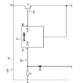
- FIG. 1 is a circuit diagram showing a configuration of a semiconductor device according to Embodiment 1;
- FIG. 2 is a plan view showing the configuration of the upper surface of the semiconductor device in Embodiment 1;
- FIG. 4 is a flow chart showing a method for manufacturing a semiconductor device according to Embodiment 1;
- 1 is a circuit diagram showing a configuration of a semiconductor device with terminals in an open state;
- FIG. 10 is a circuit diagram showing the configuration of a semiconductor device according to a second embodiment;
- FIG. 12 is a circuit diagram showing the configuration of a semiconductor device according to a fourth embodiment
- FIG. 12 is a plan view showing the structure of the upper surface of a semiconductor device according to a fourth embodiment
- 10 is a flow chart showing a method for manufacturing a semiconductor device according to Embodiment 4
- FIG. 13 is a circuit diagram showing the configuration of a semiconductor device according to a fifth embodiment
- FIG. 21 is a plan view showing the configuration of the upper surface of a semiconductor device according to a fifth embodiment
- 1 is a circuit diagram showing a configuration of a semiconductor device with terminals in an open state
- FIG. FIG. 12 is a circuit diagram showing the configuration of a semiconductor device in Embodiment 6
- FIG. 20 is a plan view showing the structure of the upper surface of a semiconductor device according to a sixth embodiment;
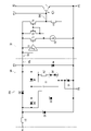
- FIG. 1 is a circuit diagram showing the configuration of a semiconductor device 101 according to the first embodiment.
- FIG. 2 is a plan view showing the configuration of the upper surface of semiconductor device 101 according to the first embodiment.
- the semiconductor device 101 includes a protection circuit A1, a control circuit B1, a switching element Z1, an input terminal P1, a terminal P2, a terminal P3, a terminal P4, and a metal wire W1 formed on one semiconductor substrate S1.
- the protection circuit A1 and the control circuit B1 may be collectively defined as one control circuit with a protection function.
- the protection circuit A1 and the control circuit B1 are formed in the circuit region 10 within the semiconductor substrate S1, and the switching element Z1 is formed in the switching element region 20 within the same semiconductor substrate S1. Although only one switching element Z1 is shown in FIG. 1, a plurality of switching elements are formed in the switching element region 20.
- the semiconductor substrate S1 is made of, for example, a semiconductor such as Si, or a so-called wide bandgap semiconductor such as SiC, GaN, or gallium oxide.
- the protection circuit A1 has a power supply voltage line VDL, a resistor R1, a Zener diode D1 and a terminal P4.
- the power supply voltage line VDL connects the input terminal P1 and the control circuit B1.
- connection means that two parts are electrically connected to each other when the semiconductor device 101 normally operates.
- a signal input from the input terminal P1 serves both as a power supply voltage for driving the control circuit B1 and as a pulse signal for controlling the state of the switching element Z1.
- the resistor R1 is provided on the power supply voltage line VDL to limit unintended currents such as rush currents.
- the cathode of the Zener diode D1 is connected to the power supply voltage line VDL.
- the terminal P4 is the anode of the Zener diode D1 and is provided on the upper surface of the semiconductor substrate S1.
- terminal P4 is a metal pad.
- the control circuit B1 controls switching between the ON state and the OFF state of the switching element Z1.
- An input portion B11 of the control circuit B1 is connected to the power supply voltage line VDL.
- the output B12 of the control circuit B1 is connected to the gate GZ1 of the switching element Z1.
- the control circuit B1 is also connected to the terminal P3.
- the switching element Z1 is, for example, an IGBT (Insulated Gate Bipolar Transistor), a MOSFET (Metal Oxide Semiconductor Field Effect Transistor), or the like.
- the switching element Z1 in FIG. 1 is an N-channel IGBT.
- the terminal P2 is a collector electrode, and is formed, for example, on the lower surface of the semiconductor substrate S1.
- a terminal P3 is an emitter electrode and is a metal pad provided on the upper surface of the semiconductor substrate S1.
- the terminal P3 is arranged separately from the terminal P4 on the upper surface of the semiconductor substrate S1.
- the terminal P3 is not short-circuited with the terminal P4 in the semiconductor substrate S1, that is, is insulated from the terminal P4.
- the metal wire W1 connects the terminal P3 and the terminal P4.
- a metal wire W1 is an external wiring.
- the external wiring is wiring that is not provided on the semiconductor substrate S1.
- Terminal P4 is not short-circuited to terminal P3 in semiconductor substrate S1, but terminals P3 and P4 are electrically connected to each other by metal wire W1.
- the terminal P3 is connected to GND. That is, the terminal P4 and the control circuit B1 are connected to GND via the terminal P3.
- the Zener diode D1 controls the power supply voltage applied to the control circuit B1 to be equal to or lower than the Zener voltage.
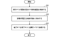
- FIG. 3 is a flow chart showing the method of manufacturing the semiconductor device 101 according to the first embodiment.
- FIG. 4 is a circuit diagram showing the configuration of the semiconductor device 101A with terminals in an open state.
- step S11 the semiconductor device 101A with the terminal P4 in an open state is prepared.
- the terminal P4 In the state before burn-in (energization test), in other words, in the initial state, the terminal P4 is not connected to the terminal P3 by the metal wire W1.
- the semiconductor device 101A in step S11 may be in a chip state or in a wafer state before dicing.
- a test voltage is applied to the control circuit B1.
- This step S12 is a so-called burn-in.
- a test voltage is applied to the control circuit B1 by being applied between the power supply voltage line VDL and the terminal P3 via the input terminal P1.
- the test voltage is applied to the control circuit B1 by being applied between the power supply voltage line VDL and the terminal P3 via the terminal P4.
- the test voltage is higher than the Zener voltage of the Zener diode D1 and below the rated voltage of the control circuit B1.
- the test voltage does not short-circuit the terminals P4 and P3.
- the terminal P4 is temporarily connected to the terminal P3 by a tester or the like. Then, the power supply voltage is applied to the control circuit B1 by applying it between the power supply voltage line VDL and the terminal P3 via the input terminal P1.
- step S13 after burn-in, terminal P4 is connected to terminal P3 with metal wire W1.
- This step S13 is a so-called wire bonding step. Through this process, the semiconductor device 101 shown in FIG. 1 is completed.
- the semiconductor device 101 includes a switching element Z1, a control circuit B1, a Zener diode D1, a terminal P4 (first terminal), a terminal P3 (second terminal) and a metal wire W1 (external wiring).
- the switching element Z1 is formed on the semiconductor substrate S1.
- the control circuit B1 is formed on the semiconductor substrate S1 including the switching element Z1, and controls the state of the switching element Z1.
- Zener diode D1 includes a cathode connected to power supply voltage line VDL between control circuit B1 and input terminal P1 to which a power supply voltage for driving control circuit B1 is input. Zener diode D1 is formed on semiconductor substrate S1.
- the terminal P4 is provided on the upper surface (main surface) of the semiconductor substrate S1 as the anode of the Zener diode D1.
- a terminal P3 is provided on the upper surface of the semiconductor substrate S1 as an emitter of the switching element Z1.
- the terminal P3 is insulated from the terminal P4 within the semiconductor substrate S1.
- a metal wire W1 connects the terminals P3 and P4.
- Such a semiconductor device 101 can apply a test voltage equal to or higher than the Zener voltage (approximately 7 V) of the Zener diode D1 to the control circuit B1 in the manufacturing process. For example, it is possible to apply a voltage close to the rated voltage of the control circuit B1 to perform burn-in. As a result, reliable screening can be completed in a short time.
- the switching element Z1 is not limited to an N-channel IGBT.
- the switching element Z1 may be an N-channel MOSFET.
- terminal P4 corresponds to the source of the N-channel MOSFET.
- a switching element whose emitter is separated may be connected for current sensing.
- External wiring is not limited to metal wires.
- the external wiring may be a flat conductor.
- the terminals P4 and P3 may be provided on the bottom surface of the semiconductor substrate S1. In that case, the external wiring may be a wiring pattern provided on a circuit board facing the lower surface of the semiconductor substrate S1.
- Embodiment 2 A semiconductor device and a method for manufacturing the semiconductor device according to the second embodiment will be described.
- the same reference numerals are given to the same components as in Embodiment 1, and detailed description thereof will be omitted.
- FIG. 5 is a circuit diagram showing the configuration of semiconductor device 102 according to the second embodiment.
- FIG. 6 is a plan view showing the configuration of the upper surface of semiconductor device 102 according to the second embodiment.
- the semiconductor device 102 includes a protection circuit A2, a control circuit B1, a switching element Z1, an input terminal P1, a terminal P2, a terminal P3, a terminal P5, a terminal P6, and a metal wire W2 formed on one semiconductor substrate S1.
- the protection circuit A2 has a power supply voltage line VDL, a resistor R1, a Zener diode D1, terminals P5 and P6.
- the cathode of the Zener diode D1 is connected to the power supply voltage line VDL.
- the anode of the Zener diode D1 is connected to the terminal P3, which is the emitter electrode of the switching element Z1.
- the terminal P5 divides the power supply voltage line VDL in the semiconductor substrate S1 between the cathode of the Zener diode D1 and the control circuit B1.
- the terminal P5 is provided on the upper surface of the semiconductor substrate S1 and is connected to the input section B11 of the control circuit B1.
- terminal P5 is a metal pad.
- the terminal P6 is the cathode of the Zener diode D1 and is provided on the upper surface of the semiconductor substrate S1.
- the terminal P6 is not short-circuited with the terminal P5 in the semiconductor substrate S1, that is, is insulated from the terminal P5.
- the terminal P6, together with the terminal P5, separates the power supply voltage line VDL in the semiconductor substrate S1 between the cathode of the Zener diode D1 and the control circuit B1.
- terminal P6 is a metal pad.
- a metal wire W2 connects the terminals P5 and P6 to form a power supply voltage line VDL. Although the terminal P6 is not short-circuited to the terminal P5 in the semiconductor substrate S1, the terminals P5 and P6 are electrically connected to each other by the metal wire W2.
- the terminal P3 is connected to GND. That is, the anode of Zener diode D1 is connected to GND via terminal P3.
- the Zener diode D1 controls the power supply voltage applied to the control circuit B1 to be equal to or lower than the Zener voltage.
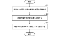
- FIG. 7 is a flow chart showing a method for manufacturing the semiconductor device 102 according to the second embodiment.
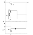
- FIG. 8 is a circuit diagram showing the configuration of a semiconductor device 102A with terminals in an open state.
- step S21 the semiconductor device 102A with the terminal P5 in an open state is prepared.
- the open state of the terminal P5 corresponds to the open state of the power supply voltage line VDL. In the state before burn-in, terminal P5 is not connected to terminal P6 by metal wire W2.
- a test voltage is applied to the control circuit B1. Specifically, the test voltage is applied to the control circuit B1 by being applied between the power supply voltage line VDL and the terminal P3 via the terminal P5. The test voltage is higher than the Zener voltage of the Zener diode D1 and below the rated voltage of the control circuit B1. Through this test, the semiconductor devices 102A that meet the specifications are screened.
- terminal P5 is connected to terminal P6 with metal wire W2.
- the semiconductor device 102 shown in FIG. 5 is completed.
- the semiconductor device 102 includes a switching element Z1, a control circuit B1, a Zener diode D1, a terminal P5 (first terminal), a terminal P6 (second terminal) and a metal wire W2 (external wiring).
- the switching element Z1 is formed on the semiconductor substrate S1.
- the control circuit B1 is formed on the semiconductor substrate S1 including the switching element Z1, and controls the state of the switching element Z1.
- Zener diode D1 includes a cathode connected to power supply voltage line VDL between control circuit B1 and input terminal P1 to which a power supply voltage for driving control circuit B1 is input.
- Zener diode D1 is formed on semiconductor substrate S1.
- the terminal P5 is provided on the upper surface of the semiconductor substrate S1.
- the terminal P5 divides the power supply voltage line VDL in the semiconductor substrate S1 between the cathode of the Zener diode D1 and the control circuit B1.
- the terminal P5 is connected to the input section B11 of the control circuit B1.
- a terminal P6 is provided on the upper surface of the semiconductor substrate S1 as a cathode of the Zener diode D1.
- the terminal P6, together with the terminal P5, separates the power supply voltage line VDL in the semiconductor substrate S1 between the cathode of the Zener diode D1 and the control circuit B1.
- a metal wire W2 connects terminals P5 and P6 to form a power supply voltage line VDL.
- Such a semiconductor device 102 can apply a test voltage equal to or higher than the Zener voltage (approximately 7 V) of the Zener diode D1 to the control circuit B1 in the manufacturing process. For example, it is possible to apply a voltage close to the rated voltage of the control circuit B1 to perform burn-in. As a result, reliable screening can be completed in a short time.
- terminal P5 is provided in the protection circuit A2 in the second embodiment, the terminal P5 may be the input section B11 of the control circuit B1 itself.
- Embodiment 3 A semiconductor device and a method for manufacturing the semiconductor device according to the third embodiment will be described.
- the same reference numerals are given to the same components as those in Embodiment 1 or 2, and detailed description thereof will be omitted.
- FIG. 9 is a circuit diagram showing the configuration of semiconductor device 103 according to the third embodiment.
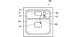
- FIG. 10 is a plan view showing the configuration of the upper surface of semiconductor device 103 according to the third embodiment.
- the semiconductor device 103 includes a protection circuit A3, a control circuit B1, a switching element Z1, an input terminal P1, a terminal P2, a terminal P3, a terminal P7, a terminal P9, and a metal wire W3 formed on one semiconductor substrate S1.
- the protection circuit A3 has an input terminal P1, a resistor R1, a resistor R2, a Zener diode D1, Schottky barrier diodes D2 to D6, a transistor T1, terminals P7 and P9.
- the configurations of input terminal P1, resistor R1 and Zener diode D1 are the same as those of the second embodiment.
- the Schottky barrier diode D2 and the transistor T1 are connected in parallel to the power supply voltage line VDL.
- the Schottky barrier diode D2 prevents latchup parasitic on elements in the circuit.
- Transistor T1 is a P-channel MOSFET. Transistor T1 reduces the voltage drop across Schottky barrier diode D2.
- the gate of transistor T1 is connected to the drain via resistor R2.
- the back gate of transistor T1 is connected to the cathodes of Schottky barrier diodes D3 and D4.
- the anode of the Schottky barrier diode D3 is connected to the emitter of the switching element Z1, that is, the terminal P3.
- the anode of Schottky barrier diode D4 is connected to input terminal P1 via the cathode of Zener diode D1 and resistor R1.
- the anode of the Schottky barrier diode D5 is connected to the input section B11 of the control circuit B1.
- the Schottky barrier diode D6 has a cathode connected to the input section B11 of the control circuit B1 and an anode connected to the terminal P3.
- the terminal P9 is connected to the power supply voltage line VDL between the drain of the transistor T1 and the input section B11 of the control circuit B1.
- the terminal P9 is provided on the upper surface of the semiconductor substrate S1.
- terminal P9 is a metal pad.
- terminal P7 is provided on the upper surface of the semiconductor substrate S1 as the gate of the transistor T1.
- terminal P7 is a metal pad.
- the terminal P3 is arranged separately from the terminal P7 on the upper surface of the semiconductor substrate S1.
- the terminal P3 is not short-circuited with the terminal P7 in the semiconductor substrate S1, that is, is insulated from the terminal P7.
- a metal wire W3 connects the terminals P3 and P7. Although the terminal P7 is not short-circuited to the terminal P3 in the semiconductor substrate S1, the terminals P3 and P7 are electrically connected to each other by the metal wire W3.
- the terminal P3 is connected to GND. That is, the anode of Zener diode D1 and terminal P7 are connected to GND via terminal P3.
- the Zener diode D1 controls the power supply voltage applied to the control circuit B1 to be equal to or lower than the Zener voltage. Also, such a configuration prevents malfunction of the back gate of the transistor T1 and the parasitic thyristor in the control circuit B1.
- FIG. 11 is a flow chart showing a method for manufacturing the semiconductor device 103 according to the third embodiment.
- FIG. 12 is a circuit diagram showing the configuration of a semiconductor device 103A with terminals in an open state.
- step S31 the semiconductor device 103A with the terminal P7 in an open state is prepared. In the state before burn-in, terminal P7 is not connected to terminal P3 by metal wire W3.
- a test voltage is applied to the control circuit B1.
- the test voltage is applied to the control circuit B1 by applying it between the terminal P9 and the terminal P3 provided on the power supply voltage line VDL.
- Terminal P7 which is the gate of transistor T1
- Terminal P7 which is the gate of transistor T1
- terminal P3 is not connected to terminal P3 as described above.
- resistor R2 between the gate and drain of transistor T1. Therefore, when the test voltage is applied between the terminal P9 and the terminal P3, the transistor T1 will not be driven.
- a test voltage whose maximum value is the breakdown voltage (about 16 V) of the Schottky barrier diode D6 is applied to the control circuit B1. Through this test, the semiconductor devices 103A that meet the specifications are screened.
- the test voltage may be applied to the control circuit B1 by being applied between the power supply voltage line VDL and the terminal P3 via the terminal P7, for example.
- terminal P7 is connected to terminal P3 with metal wire W3.
- the semiconductor device 103 shown in FIG. 9 is completed.
- the gate of transistor T1 is connected to the emitter of switching element Z1, ie, terminal P3.
- Transistor T1 reduces the forward voltage drop of Schottky barrier diode D2.
- the semiconductor device 103 includes a switching element Z1, a control circuit B1, a Zener diode D1, a transistor T1, a resistor R2, a terminal P7 (first terminal), a terminal P3 (second terminal), and a metal A wire W3 (external wiring) is provided.
- the switching element Z1 is formed on the semiconductor substrate S1.
- the control circuit B1 is formed on the semiconductor substrate S1 including the switching element Z1, and controls the state of the switching element Z1.
- Zener diode D1 includes a cathode connected to power supply voltage line VDL between control circuit B1 and input terminal P1 to which a power supply voltage for driving control circuit B1 is input. Zener diode D1 is formed on semiconductor substrate S1.
- the transistor T1 is formed on the semiconductor substrate S1 and connected in parallel to the power supply voltage line VDL.
- the resistor R2 is formed on the semiconductor substrate S1 and provided between the gate and drain of the transistor T1.
- the terminal P7 is provided on the upper surface of the semiconductor substrate S1 as the gate of the transistor T1.
- a terminal P3 is provided on the upper surface of the semiconductor substrate S1 as an emitter of the switching element Z1 and is insulated from the terminal P7.
- a metal wire W3 connects the terminals P7 and P3.
- Such a semiconductor device 103 enables burn-in by applying a voltage close to the rated voltage of the control circuit B1 to the control circuit B1 in the manufacturing process. Since a voltage higher than the Zener voltage of the Zener diode D1 for input protection is applied, reliable screening is completed in a short time.
- Embodiment 4 A semiconductor device and a method for manufacturing the semiconductor device according to the fourth embodiment will be described.
- the same reference numerals are given to the same constituent elements as in any one of Embodiments 1 to 3, and detailed description thereof will be omitted.
- FIG. 13 is a circuit diagram showing the configuration of semiconductor device 104 according to the fourth embodiment.
- FIG. 14 is a plan view showing the configuration of the upper surface of semiconductor device 104 according to the fourth embodiment.
- the semiconductor device 104 includes a protection circuit A4, a control circuit B1, a switching element Z1, an input terminal P1, a terminal P2, a terminal P3, a terminal P8 and a terminal P9 formed on one semiconductor substrate S1.
- the protection circuit A4 further includes a Zener diode D7 and a bidirectional Zener diode D8 in addition to the configuration of the protection circuit A3 of the third embodiment.
- Zener diode D7 includes a cathode connected to the gate of transistor T1 and an anode connected to the emitter of switching element Z1.
- the Zener diode D7 is short-circuited (Zener zapped). That is, the gate of transistor T1 is short-circuited with terminal P3.
- a bidirectional Zener diode D8 is provided between the gate and drain of the transistor T1 and connected in series with the resistor R2.
- the bidirectional Zener diode D8 reduces heat generated in each element in the current path when the test voltage is applied to the control circuit B1 in the manufacturing process of the semiconductor device 104.
- FIG. The heat is generated by overvoltage or overcurrent, and causes damage to each element.
- the degree of heat generation reduction can be adjusted by the number of bidirectional Zener diodes D8 connected. If the heat generation is small, the bidirectional Zener diode D8 is not necessarily required.
- terminal P8 is provided on the upper surface of the semiconductor substrate S1 as the gate of the transistor T1.
- terminal P8 is a metal pad.
- a metal wire or the like is not connected to the terminal P8.
- the terminal P3 is arranged separately from the terminal P8 on the upper surface of the semiconductor substrate S1.
- the terminal P3 is not short-circuited with the terminal P8 in the semiconductor substrate S1, that is, is insulated from the terminal P8.
- the anode of the Zener diode D1 is connected to GND via the terminal P3.
- the Zener diode D1 controls the power supply voltage applied to the control circuit B1 to be equal to or lower than the Zener voltage. Further, since the Zener diode D7 is short-circuited (Zener zapped), the gate of the transistor T1 is also connected to GND via the terminal P3. Transistor T1 reduces the forward voltage drop of Schottky barrier diode D2.
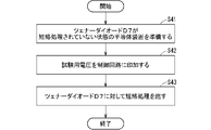
- FIG. 15 is a flow chart showing a method for manufacturing the semiconductor device 104 according to the fourth embodiment.
- step S41 a semiconductor device is prepared in which the Zener diode D7 is not short-circuited.
- the gate of transistor T1 is isolated from terminal P3 within a predetermined voltage range by Zener diode D7.
- a test voltage is applied to the control circuit B1.
- the test voltage is applied to the control circuit B1 by applying it between the terminals P9 and P3. No current flows from the gate of transistor T1 to terminal P3.
- a resistor R2 also exists between the gate and the drain of the transistor T1. Therefore, when the test voltage is applied via the terminal P9, the transistor T1 will not be driven.
- a test voltage whose maximum value is the breakdown voltage (about 16 V) of the Schottky barrier diode D6 is applied to the control circuit B1. At this time, a voltage of about 9 V is applied between the gate and drain of the transistor T1. This test screens for semiconductor devices that meet the specifications.
- step S43 after burn-in, the Zener diode D7 is short-circuited (zener zap).
- a voltage of about 35 V, for example, is applied as a short-circuiting voltage between the gate of the transistor T1 and the emitter of the switching element Z1.
- the voltage between the gate and the drain of the transistor T1 is about 19V.
- a bidirectional Zener diode D8 is connected between the gate and drain of transistor T1 so that each element in the current path can withstand heat generation.
- the Zener zap shorts the gate of transistor T1 to the emitter of switching element Z1, ie terminal P3.
- Transistor T1 reduces the forward voltage drop of Schottky barrier diode D2.
- the semiconductor device 104 includes a switching element Z1, a control circuit B1, a Zener diode D1, a transistor T1, a resistor R2, a Zener diode D7 (short circuit processing Zener diode), and a terminal P8 (gate terminal ) and
- the switching element Z1 is formed on the semiconductor substrate S1.
- the control circuit B1 is formed on the semiconductor substrate S1 including the switching element Z1, and controls the state of the switching element Z1.
- Zener diode D1 includes a cathode connected to power supply voltage line VDL between control circuit B1 and input terminal P1 to which a power supply voltage for driving control circuit B1 is input. Zener diode D1 is formed on semiconductor substrate S1.
- the transistor T1 is formed on the semiconductor substrate S1 and connected in parallel to the power supply voltage line VDL.
- the resistor R2 is formed on the semiconductor substrate S1 and provided between the gate and drain of the transistor T1.
- Zener diode D7 includes a cathode connected to the gate of transistor T1 and an anode connected to the emitter of switching element Z1. Zener diode D7 is short-circuited.
- a terminal P8 is provided on the upper surface of the semiconductor substrate S1 as a gate of the transistor T1.
- Such a semiconductor device 104 makes it possible to perform burn-in by applying a voltage close to the rated voltage of the control circuit B1 to the control circuit B1 in the manufacturing process. Since a voltage higher than the Zener voltage of the Zener diode D1 for input protection is applied, reliable screening is completed in a short time. Cost is reduced because a wire bonding process is not required for electrically connecting the gate of the transistor T1 and the emitter of the switching element Z1.
- Embodiment 5 A semiconductor device and a method for manufacturing the semiconductor device according to the fifth embodiment will be described.
- the same reference numerals are given to the same components as in any one of Embodiments 1 to 4, and detailed description thereof will be omitted.
- FIG. 16 is a circuit diagram showing the configuration of semiconductor device 105 according to the fifth embodiment.
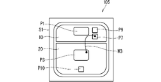
- FIG. 17 is a plan view showing the configuration of the upper surface of semiconductor device 105 according to the fifth embodiment.
- the semiconductor device 105 includes a protection circuit A3, a control circuit B2, a switching element Z1, an input terminal P1, a terminal P2, a terminal P3, a terminal P7, a terminal P9, a terminal P10, and a metal wire W3 formed on one semiconductor substrate S1. .
- the control circuit B2 includes a waveform shaping circuit C1, a P-channel MOSFET (T2), a P-channel MOSFET (T3), a P-channel MOSFET (T4), a constant current source C2 and a resistor R3.
- the P-channel MOSFET (T2) is driven by the output of the waveform shaping circuit C1.
- the source of the P-channel MOSFET (T3) is shared with the drain of the P-channel MOSFET (T2) and connected to the constant current source C2.
- the gate of the P-channel MOSFET (T4) is common with the P-channel MOSFET (T3).
- the P-channel MOSFET (T4) and P-channel MOSFET (T3) form a current mirror circuit.
- the drain of the P-channel MOSFET (T4) is connected to the gate GZ1 of the switching element Z1.
- a resistor R3 connects the gate of the transistor T1, the gate GZ1 of the switching element Z1 and the drain of the P-channel MOSFET (T4) to each other.
- the protection circuit A3 has the configuration shown in the third embodiment. Although the terminal P7 is not short-circuited to the terminal P3 in the semiconductor substrate S1, the terminals P3 and P7 are electrically connected to each other by the metal wire W3. As in the fourth embodiment, a bidirectional Zener diode D8 may be connected between the gate of transistor T1 and resistor R2, if necessary.
- terminal P10 is provided on the upper surface of the semiconductor substrate S1 as a gate electrode of the switching element Z1.
- terminal P10 is a metal pad.
- the anode of the Zener diode D1 and the terminal P7 are connected to GND via the terminal P3.
- a voltage signal is input to the input terminal P1.
- a power supply voltage is generated based on the voltage signal, and Zener diode D1 controls the power supply voltage below the Zener voltage.
- the waveform shaping circuit C1 is turned on based on the power supply voltage.
- the H signal is transmitted to the gate of the P-channel MOSFET (T2), turning off the P-channel MOSFET (T2).
- a current flows from the constant current source C2 to the P-channel MOSFET (T3). Due to the current mirror configuration, a copied or amplified current flows in the P-channel MOSFET (T4).
- Current flows through resistor R3.
- a gate voltage is applied to the gate GZ1 of the switching element Z1, and current flows from the terminal P3, which is the emitter electrode, to the terminal P2, which is the collector electrode.
- the blocking operation is the reverse of (i) to (iii) above.
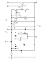
- FIG. 18 is a circuit diagram showing the configuration of a semiconductor device 105A with open terminals.
- step S31 the semiconductor device 105A with the terminal P7 in an open state is prepared. In the state before burn-in, terminal P7 is not connected to terminal P3 by metal wire W3.
- a test voltage is applied to the control circuit B2.
- the test voltage is applied to the control circuit B2 by applying it between the terminal P9 and the terminal P3.
- a test voltage having a maximum value of the withstand voltage (approximately 16 V) of the Schottky barrier diode D6 is applied to the control circuit B2.
- a gate oxide film screening voltage (hereinafter referred to as a gate oxide film test voltage) is applied between terminals P10 and P3.
- a gate oxide film test voltage For example, when the thickness of the gate oxide film of the switching element Z1 is 500 ⁇ , it is preferable to apply a gate oxide film test voltage near the withstand voltage (50 V) of the oxide film.
- a gate oxide film test voltage of 40V when a gate oxide film test voltage of 40V is applied between terminals P10 and P3, current flows through the path of resistor R3-resistor R2-Schottky barrier diode D6.
- the Schottky barrier diode D6 has a withstand voltage of about 16V, a voltage of 24V is applied to the resistors R2 and R3 together.
- Bidirectional Zener diode D8 reduces heat generation in resistors R2 and R3. The degree of heat generation reduction can be adjusted by the number of bidirectional Zener diodes D8 connected.
- the gate oxide film test voltage is applied through the terminal P10. A gate oxide test voltage may be applied to .
- the semiconductor device 105A that satisfies the specifications is screened by the test in step S32.
- terminal P7 is connected to terminal P3 with metal wire W3.
- the semiconductor device 105 shown in FIG. 16 is completed.
- the transistor T1 reduces the voltage drop across the Schottky barrier diode D2.
- such a connection configuration enables the state of the switching element Z1 to be controlled by a signal input from the input terminal P1.
- the semiconductor device 105 according to the fifth embodiment has, in addition to the structure of the semiconductor device 103 according to the third embodiment, a resistor R3 (for voltage generation) connecting the gate of the transistor T1 and the gate GZ1 of the switching element Z1. resistance).
- Such a semiconductor device 105 enables not only screening of the control circuit B2 but also screening of the gate oxide film of the switching element Z1. This improves selectability regarding the presence/absence of defects in the semiconductor device 105A.
- the semiconductor device 105 may further include a P-channel MOSFET (not shown) that is connected in parallel with the P-channel MOSFET (T3) and driven during malfunction. Malfunction is, for example, malfunction at high temperature or overvoltage. This enhances the protection function.
- Embodiment 6 A semiconductor device and a method for manufacturing the semiconductor device according to the sixth embodiment will be described.
- the same reference numerals are given to the same components as in any of Embodiments 1 to 5, and detailed description thereof will be omitted.
- FIG. 19 is a circuit diagram showing the configuration of the semiconductor device 106 according to the sixth embodiment.
- FIG. 20 is a plan view showing the configuration of the upper surface of semiconductor device 106 in accordance with the sixth embodiment.
- the semiconductor device 106 includes a protection circuit A4, a control circuit B2, a switching element Z1, an input terminal P1, a terminal P2, a terminal P3, a terminal P8, a terminal P9 and a terminal P10 formed on one semiconductor substrate S1.
- Zener diode D7 includes a cathode connected to the gate of transistor T1 and an anode connected to the emitter of switching element Z1. Zener diode D7 is short-circuited. Also, a bidirectional Zener diode D8 is provided as required. A terminal P8 is provided on the upper surface of the semiconductor substrate S1 as a gate of the transistor T1. A metal wire or the like is not connected to the terminal P8. The terminal P3 is not short-circuited with the terminal P8 in the semiconductor substrate S1, that is, is insulated from the terminal P8.
- the control circuit B2 has the configuration shown in the fifth embodiment. That is, the resistor R3 connects the gate of the transistor T1, the gate GZ1 of the switching element Z1, and the drain of the P-channel MOSFET (T4).
- a method for manufacturing the semiconductor device 106 according to the sixth embodiment is the same as the flowchart shown in FIG.
- step S41 a semiconductor device is prepared in which the Zener diode D7 is not short-circuited.
- a test voltage is applied to the control circuit B2.
- the test voltage is applied to the control circuit B2 by applying it between the terminal P9 and the terminal P3.
- a resistor R2 also exists between the gate and the drain of the transistor T1. Therefore, when the test voltage is applied via the terminal P9, the transistor T1 will not be driven.
- a voltage approximately 16 V
- a voltage of about 9 V is applied between the gate and drain of transistor T1.
- step S43 after burn-in, the Zener diode D7 is short-circuited (zener zap). At this time, a voltage of about 35 V, for example, is applied between the gate of the transistor T1 and the emitter of the switching element Z1 as a short-circuiting voltage. The voltage between the gate and drain of transistor T1 is approximately 19V.
- Bidirectional Zener diode D8 reduces heat generation of each element in the current path. The degree of reduction can be adjusted by the number of bidirectional Zener diodes D8 connected.
- the semiconductor device 106 according to the sixth embodiment has, in addition to the structure of the semiconductor device 104 according to the third embodiment, a resistor R3 (for voltage generation) connecting the gate of the transistor T1 and the gate GZ1 of the switching element Z1. resistance).
- Such a semiconductor device 106 enables not only screening of the control circuit B2 but also screening of the gate oxide film of the switching element Z1. The selectability of the presence/absence of defects in the semiconductor device 106 is improved.
Landscapes
- Semiconductor Integrated Circuits (AREA)
- Electronic Switches (AREA)
Abstract
Description
(半導体装置の構成)
図1は、実施の形態1における半導体装置101の構成を示す回路図である。図2は、実施の形態1における半導体装置101の上面における構成を示す平面図である。
図3は、実施の形態1における半導体装置101の製造方法を示すフローチャートである。図4は、端子が開放状態の半導体装置101Aの構成を示す回路図である。
実施の形態2における半導体装置および半導体装置の製造方法を説明する。実施の形態2において、実施の形態1と同様の構成要素には、同一の参照符号を付し、それらの詳細な説明は省略する。
図5は、実施の形態2における半導体装置102の構成を示す回路図である。図6は、実施の形態2における半導体装置102の上面における構成を示す平面図である。
図7は、実施の形態2における半導体装置102の製造方法を示すフローチャートである。図8は、端子が開放状態の半導体装置102Aの構成を示す回路図である。
実施の形態3における半導体装置および半導体装置の製造方法を説明する。実施の形態3において、実施の形態1または2と同様の構成要素には、同一の参照符号を付し、それらの詳細な説明は省略する。
図9は、実施の形態3における半導体装置103の構成を示す回路図である。図10は、実施の形態3における半導体装置103の上面における構成を示す平面図である。
図11は、実施の形態3における半導体装置103の製造方法を示すフローチャートである。図12は、端子が開放状態の半導体装置103Aの構成を示す回路図である。
実施の形態4における半導体装置および半導体装置の製造方法を説明する。実施の形態4において、実施の形態1から3のいずれかと同様の構成要素には、同一の参照符号を付し、それらの詳細な説明は省略する。
図13は、実施の形態4における半導体装置104の構成を示す回路図である。図14は、実施の形態4における半導体装置104の上面における構成を示す平面図である。
図15は、実施の形態4における半導体装置104の製造方法を示すフローチャートである。
実施の形態5における半導体装置および半導体装置の製造方法を説明する。実施の形態5において、実施の形態1から4のいずれかと同様の構成要素には、同一の参照符号を付し、それらの詳細な説明は省略する。
図16は、実施の形態5における半導体装置105の構成を示す回路図である。図17は、実施の形態5における半導体装置105の上面における構成を示す平面図である。
(i)入力端子P1に電圧信号が入力される。電源電圧はその電圧信号に基づいて生成され、ツェナーダイオードD1は、電源電圧をツェナー電圧以下に制御する。(ii)その電源電圧に基づいて、波形整形回路C1がON状態となる。H信号がPチャネルMOSFET(T2)のゲートに伝達され、PチャネルMOSFET(T2)がOFF状態になる。定電流源C2からPチャネルMOSFET(T3)に電流が流れる。カレントミラーの構成により、PチャネルMOSFET(T4)にコピーされた電流または増幅された電流が流れる。(iii)抵抗R3に電流が流れる。スイッチング素子Z1のゲートGZ1にゲート電圧が印加され、エミッタ電極である端子P3からコレクタ電極である端子P2に電流が流れる。遮断動作は、上記の(i)から(iii)の逆である。
実施の形態5における半導体装置105の製造方法は、図11に示されるフローチャートと同様である。図18は、端子が開放状態の半導体装置105Aの構成を示す回路図である。
実施の形態6における半導体装置および半導体装置の製造方法を説明する。実施の形態6において、実施の形態1から5のいずれかと同様の構成要素には、同一の参照符号を付し、それらの詳細な説明は省略する。
実施の形態6における半導体装置106の製造方法は、図15に示されるフローチャートと同様である。
Claims (18)
- 半導体基板に形成されたスイッチング素子と、
前記スイッチング素子を含む前記半導体基板に形成され、前記スイッチング素子の状態を制御する制御回路と、
前記制御回路を駆動させるための電源電圧が入力される入力端子と前記制御回路との間の電源電圧ラインに接続されたカソードを含み、前記半導体基板に形成されたツェナーダイオードと、
前記ツェナーダイオードのアノードとして前記半導体基板の主面に設けられた第1端子と、
前記スイッチング素子のエミッタおよびソースのうちいずれか一方として前記半導体基板の前記主面に設けられ、前記半導体基板内で前記第1端子から絶縁されている第2端子と、を備える、半導体装置。 - 前記第1端子と前記第2端子とを接続する外部配線を、さらに備える請求項1に記載の半導体装置。
- スイッチング素子と、前記スイッチング素子の状態を制御する制御回路と、前記制御回路を駆動させるための電源電圧が入力される入力端子と前記制御回路との間の電源電圧ラインに接続されたカソードを含むツェナーダイオードと、が1つの半導体基板に形成されており、前記ツェナーダイオードのアノードとして前記半導体基板の主面に設けられた第1端子と、前記スイッチング素子のエミッタおよびソースのうちいずれか一方として前記半導体基板の前記主面に設けられ前記半導体基板内で前記第1端子から絶縁された第2端子と、を含む半導体装置を準備する工程と、
前記第1端子を介して前記制御回路に試験用電圧を印加して、または、前記アノードが開放状態である場合に前記入力端子を介して前記制御回路に試験用電圧を印加して、前記制御回路を試験する工程と、備える半導体装置の製造方法。 - 前記第1端子と前記第2端子とを外部配線で接続する工程を、さらに備える請求項3に記載の半導体装置の製造方法。
- 半導体基板に形成されたスイッチング素子と、
前記スイッチング素子を含む前記半導体基板に形成され、前記スイッチング素子の状態を制御する制御回路と、
前記制御回路を駆動させるための電源電圧が入力される入力端子と前記制御回路との間の電源電圧ラインに接続されたカソードを含み、前記半導体基板に形成されたツェナーダイオードと、
前記半導体基板の主面に設けられ、前記半導体基板内の前記電源電圧ラインを前記ツェナーダイオードの前記カソードと前記制御回路との間で分断し、前記制御回路の入力部に接続されている第1端子と、
前記ツェナーダイオードの前記カソードとして前記半導体基板の前記主面に設けられ、前記第1端子とともに、前記半導体基板内の前記電源電圧ラインを前記ツェナーダイオードの前記カソードと前記制御回路との間で分断している第2端子と、を備える、半導体装置。 - 前記第1端子と前記第2端子とを接続して、前記電源電圧ラインを形成している外部配線を、さらに備える請求項5に記載の半導体装置。
- スイッチング素子と、前記スイッチング素子の状態を制御する制御回路と、前記制御回路を駆動させるための電源電圧が入力される入力端子と前記制御回路との間の電源電圧ラインに接続されたカソードを含むツェナーダイオードと、が1つの半導体基板に形成されており、前記半導体基板の主面に設けられ前記半導体基板内の前記電源電圧ラインを前記ツェナーダイオードの前記カソードと前記制御回路との間で分断し前記制御回路の入力部に接続されている第1端子と、前記ツェナーダイオードの前記カソードとして前記半導体基板の前記主面に設けられ、前記第1端子とともに前記半導体基板内の前記電源電圧ラインを前記ツェナーダイオードの前記カソードと前記制御回路との間で分断している第2端子と、を含む半導体装置を準備する工程と、
前記第1端子を介して前記制御回路に試験用電圧を印加して、前記制御回路を試験する工程と、を備える半導体装置の製造方法。 - 前記第1端子と前記第2端子とを、外部配線で接続して、前記電源電圧ラインを形成する工程を、さらに備える請求項7に記載の半導体装置の製造方法。
- 半導体基板に形成されたスイッチング素子と、
前記スイッチング素子を含む前記半導体基板に形成され、前記スイッチング素子の状態を制御する制御回路と、
前記制御回路を駆動させるための電源電圧が入力される入力端子と前記制御回路との間の電源電圧ラインに接続されたカソードを含み、前記半導体基板に形成されたツェナーダイオードと、
前記半導体基板に形成され、前記電源電圧ラインに並列に接続されたトランジスタと、
前記半導体基板に形成され、前記トランジスタのゲートとドレインとの間に設けられた抵抗と、
前記トランジスタの前記ゲートとして前記半導体基板の主面に設けられた第1端子と、
前記スイッチング素子のエミッタおよびソースのうちいずれか一方として前記半導体基板の前記主面に設けられ、前記半導体基板内で前記第1端子から絶縁された第2端子と、を備える、半導体装置。 - 前記第1端子と前記第2端子とを接続する外部配線を、さらに備える請求項9に記載の半導体装置。
- 前記トランジスタの前記ゲートと前記スイッチング素子の前記ゲートとを接続する電圧発生用抵抗を、さらに備える請求項9または請求項10に記載の半導体装置。
- スイッチング素子と、前記スイッチング素子の駆動を制御する制御回路と、前記制御回路を駆動させるための電源電圧が入力される入力端子と前記制御回路との間の電源電圧ラインに接続されたカソードを含むツェナーダイオードと、前記電源電圧ラインに並列に接続されたトランジスタと、前記トランジスタのゲートとドレインとの間に設けられた抵抗と、が1つの半導体基板に形成されており、前記トランジスタの前記ゲートとして前記半導体基板の主面に設けられた第1端子と、前記スイッチング素子のエミッタおよびソースのうちいずれか一方として前記半導体基板の前記主面に設けられ前記半導体基板内で前記第1端子から絶縁された第2端子と、を含む半導体装置を準備する工程と、
前記第1端子を介して前記制御回路に試験用電圧を印加して、または、前記トランジスタの前記ドレインと前記制御回路との間の前記電源電圧ラインに接続された第3端子を介して前記制御回路に試験用電圧を印加して、前記制御回路を試験する工程と、備える半導体装置の製造方法。 - 前記第1端子と前記第2端子とを、外部配線で接続する工程を、さらに備える請求項12に記載の半導体装置の製造方法。
- 半導体基板に形成されたスイッチング素子と、
前記スイッチング素子を含む前記半導体基板に形成され、前記スイッチング素子の状態を制御する制御回路と、
前記制御回路を駆動させるための電源電圧が入力される入力端子と前記制御回路との間の電源電圧ラインに接続されたカソードを含み、前記半導体基板に形成されたツェナーダイオードと、
前記半導体基板に形成され、前記電源電圧ラインに並列に接続されたトランジスタと、
前記半導体基板に形成され、前記トランジスタのゲートとドレインとの間に設けられた抵抗と、
前記半導体基板に形成され、前記トランジスタの前記ゲートに接続されるカソードと、前記スイッチング素子のエミッタおよびソースのうちいずれか一方に接続されるアノードと、を含む短絡処理用ツェナーダイオードと、
前記トランジスタの前記ゲートとして前記半導体基板の主面に設けられたゲート端子と、を備える半導体装置。 - 前記短絡処理用ツェナーダイオードが、短絡処理されている請求項14に記載の半導体装置。
- 前記トランジスタの前記ゲートと前記スイッチング素子の前記ゲートと接続する電圧発生用抵抗を、さらに備える請求項14または請求項15に記載の半導体装置。
- スイッチング素子と、前記スイッチング素子の駆動を制御する制御回路と、前記制御回路を駆動させるための電源電圧が入力される入力端子と前記制御回路との間の電源電圧ラインに接続されたカソードを含むツェナーダイオードと、前記電源電圧ラインに並列に接続されたトランジスタと、前記トランジスタのゲートとドレインとの間に設けられた抵抗と、前記トランジスタの前記ゲートに接続されるカソードと前記スイッチング素子のエミッタおよびソースのうちいずれか一方に接続されるアノードとを含む短絡処理用ツェナーダイオードと、が1つの半導体基板に形成されており、前記トランジスタの前記ゲートとして前記半導体基板の主面に設けられたゲート端子を、含む半導体装置を準備する工程と、
前記ゲート端子を介して前記制御回路に試験用電圧を印加して、または、前記トランジスタの前記ドレインと前記制御回路との間の前記電源電圧ラインに接続された第3端子を介して前記制御回路に試験用電圧を印加して、前記制御回路を試験する工程と、備える半導体装置の製造方法。 - 前記短絡処理用ツェナーダイオードに短絡処理用電圧を印加する工程を、さらに備える請求項17に記載の半導体装置の製造方法。
Priority Applications (5)
| Application Number | Priority Date | Filing Date | Title |
|---|---|---|---|
| US18/252,244 US20230420445A1 (en) | 2021-02-19 | 2021-02-19 | Semiconductor device and method of manufacturing semiconductor device |
| CN202180093686.1A CN116888740A (zh) | 2021-02-19 | 2021-02-19 | 半导体装置以及半导体装置的制造方法 |
| DE112021007125.4T DE112021007125T5 (de) | 2021-02-19 | 2021-02-19 | Halbleitervorrichtung und Verfahren zum Herstellen einer Halbleitervorrichtung |
| PCT/JP2021/006252 WO2022176141A1 (ja) | 2021-02-19 | 2021-02-19 | 半導体装置および半導体装置の製造方法 |
| JP2023500252A JP7286044B2 (ja) | 2021-02-19 | 2021-02-19 | 半導体装置および半導体装置の製造方法 |
Applications Claiming Priority (1)
| Application Number | Priority Date | Filing Date | Title |
|---|---|---|---|
| PCT/JP2021/006252 WO2022176141A1 (ja) | 2021-02-19 | 2021-02-19 | 半導体装置および半導体装置の製造方法 |
Publications (1)
| Publication Number | Publication Date |
|---|---|
| WO2022176141A1 true WO2022176141A1 (ja) | 2022-08-25 |
Family
ID=82930434
Family Applications (1)
| Application Number | Title | Priority Date | Filing Date |
|---|---|---|---|
| PCT/JP2021/006252 Ceased WO2022176141A1 (ja) | 2021-02-19 | 2021-02-19 | 半導体装置および半導体装置の製造方法 |
Country Status (5)
| Country | Link |
|---|---|
| US (1) | US20230420445A1 (ja) |
| JP (1) | JP7286044B2 (ja) |
| CN (1) | CN116888740A (ja) |
| DE (1) | DE112021007125T5 (ja) |
| WO (1) | WO2022176141A1 (ja) |
Citations (4)
| Publication number | Priority date | Publication date | Assignee | Title |
|---|---|---|---|---|
| JPH11177087A (ja) * | 1997-12-09 | 1999-07-02 | Hitachi Ltd | 半導体集積回路装置の製造方法および半導体集積回路装置 |
| JP2012129252A (ja) * | 2010-12-13 | 2012-07-05 | Toyota Motor Corp | 半導体集積回路 |
| JP2014013796A (ja) * | 2012-07-03 | 2014-01-23 | Fuji Electric Co Ltd | ワンチップイグナイタ及び内燃機関点火装置 |
| JP2016009774A (ja) * | 2014-06-25 | 2016-01-18 | ルネサスエレクトロニクス株式会社 | 半導体装置 |
Family Cites Families (1)
| Publication number | Priority date | Publication date | Assignee | Title |
|---|---|---|---|---|
| US9447767B2 (en) * | 2012-07-03 | 2016-09-20 | Fuji Electric Co., Ltd. | Single chip igniter and internal combustion engine ignition device |
-
2021
- 2021-02-19 DE DE112021007125.4T patent/DE112021007125T5/de active Pending
- 2021-02-19 US US18/252,244 patent/US20230420445A1/en active Pending
- 2021-02-19 JP JP2023500252A patent/JP7286044B2/ja active Active
- 2021-02-19 WO PCT/JP2021/006252 patent/WO2022176141A1/ja not_active Ceased
- 2021-02-19 CN CN202180093686.1A patent/CN116888740A/zh active Pending
Patent Citations (4)
| Publication number | Priority date | Publication date | Assignee | Title |
|---|---|---|---|---|
| JPH11177087A (ja) * | 1997-12-09 | 1999-07-02 | Hitachi Ltd | 半導体集積回路装置の製造方法および半導体集積回路装置 |
| JP2012129252A (ja) * | 2010-12-13 | 2012-07-05 | Toyota Motor Corp | 半導体集積回路 |
| JP2014013796A (ja) * | 2012-07-03 | 2014-01-23 | Fuji Electric Co Ltd | ワンチップイグナイタ及び内燃機関点火装置 |
| JP2016009774A (ja) * | 2014-06-25 | 2016-01-18 | ルネサスエレクトロニクス株式会社 | 半導体装置 |
Also Published As
| Publication number | Publication date |
|---|---|
| US20230420445A1 (en) | 2023-12-28 |
| JPWO2022176141A1 (ja) | 2022-08-25 |
| CN116888740A (zh) | 2023-10-13 |
| DE112021007125T5 (de) | 2023-12-21 |
| JP7286044B2 (ja) | 2023-06-02 |
Similar Documents
| Publication | Publication Date | Title |
|---|---|---|
| US9041456B2 (en) | Power semiconductor device | |
| US8729566B2 (en) | Semiconductor switching arrangement having a normally on and a normally off transistor | |
| US8351172B2 (en) | Power supply control apparatus | |
| JP3610890B2 (ja) | 電気負荷駆動回路 | |
| JP5556726B2 (ja) | スイッチング回路 | |
| US10547250B2 (en) | Rectifier device | |
| US10014852B2 (en) | High-voltage stacked transistor circuit | |
| CN104051453A (zh) | 有源esd保护电路 | |
| JP2018117110A (ja) | 基板電圧制御回路 | |
| CN107852159A (zh) | 驱动装置 | |
| CN112889151B (zh) | 微调电路和微调方法 | |
| JP6065721B2 (ja) | 駆動回路、半導体集積回路、及び駆動回路の制御方法 | |
| KR20070056053A (ko) | 반도체 스위치 장치 및 전자 디바이스 | |
| JP2015149508A (ja) | 電力用半導体装置 | |
| JP2019103015A (ja) | 電源逆接続保護機能を備えた負荷駆動回路 | |
| US20170207213A1 (en) | Power Module with MOSFET Body Diode on which Energization Test can be Conducted Efficiently | |
| JP2009207077A (ja) | 半導体集積回路装置 | |
| US10784795B1 (en) | Conversion circuit | |
| US9425188B2 (en) | Active ESD protection circuit with blocking diode | |
| US5654863A (en) | Integrated circuit having a gate oxide | |
| US10784770B2 (en) | Conversion circuit | |
| CN102640419A (zh) | 半导体器件 | |
| JP7286044B2 (ja) | 半導体装置および半導体装置の製造方法 | |
| US7411770B2 (en) | Circuit arrangement with at least two semiconductor switches and a central overvoltage protection | |
| CN118889351A (zh) | 准静态esd箝位电路 |
Legal Events
| Date | Code | Title | Description |
|---|---|---|---|
| 121 | Ep: the epo has been informed by wipo that ep was designated in this application |
Ref document number: 21926574 Country of ref document: EP Kind code of ref document: A1 |
|
| ENP | Entry into the national phase |
Ref document number: 2023500252 Country of ref document: JP Kind code of ref document: A |
|
| WWE | Wipo information: entry into national phase |
Ref document number: 18252244 Country of ref document: US |
|
| WWE | Wipo information: entry into national phase |
Ref document number: 202180093686.1 Country of ref document: CN |
|
| WWE | Wipo information: entry into national phase |
Ref document number: 112021007125 Country of ref document: DE |
|
| 122 | Ep: pct application non-entry in european phase |
Ref document number: 21926574 Country of ref document: EP Kind code of ref document: A1 |