WO2022172324A1 - 表示ユニット及び表示装置 - Google Patents
表示ユニット及び表示装置 Download PDFInfo
- Publication number
- WO2022172324A1 WO2022172324A1 PCT/JP2021/004773 JP2021004773W WO2022172324A1 WO 2022172324 A1 WO2022172324 A1 WO 2022172324A1 JP 2021004773 W JP2021004773 W JP 2021004773W WO 2022172324 A1 WO2022172324 A1 WO 2022172324A1
- Authority
- WO
- WIPO (PCT)
- Prior art keywords
- light emitting
- emitting element
- display unit
- light
- height
- Prior art date
Links
- 239000000758 substrate Substances 0.000 claims abstract description 64
- 230000000052 comparative effect Effects 0.000 description 15
- 238000010586 diagram Methods 0.000 description 15
- 238000004519 manufacturing process Methods 0.000 description 13
- 230000006866 deterioration Effects 0.000 description 9
- 229920005989 resin Polymers 0.000 description 6
- 239000011347 resin Substances 0.000 description 6
- 238000005070 sampling Methods 0.000 description 6
- 238000001746 injection moulding Methods 0.000 description 4
- 239000003086 colorant Substances 0.000 description 3
- 230000004048 modification Effects 0.000 description 3
- 238000012986 modification Methods 0.000 description 3
- 230000000903 blocking effect Effects 0.000 description 2
- 230000015556 catabolic process Effects 0.000 description 2
- 238000006731 degradation reaction Methods 0.000 description 2
- 230000000694 effects Effects 0.000 description 2
- 239000011159 matrix material Substances 0.000 description 2
- 239000003822 epoxy resin Substances 0.000 description 1
- 239000003365 glass fiber Substances 0.000 description 1
- 239000002184 metal Substances 0.000 description 1
- 229920000647 polyepoxide Polymers 0.000 description 1
Images


Classifications
-
- G—PHYSICS
- G09—EDUCATION; CRYPTOGRAPHY; DISPLAY; ADVERTISING; SEALS
- G09F—DISPLAYING; ADVERTISING; SIGNS; LABELS OR NAME-PLATES; SEALS
- G09F9/00—Indicating arrangements for variable information in which the information is built-up on a support by selection or combination of individual elements
- G09F9/30—Indicating arrangements for variable information in which the information is built-up on a support by selection or combination of individual elements in which the desired character or characters are formed by combining individual elements
- G09F9/302—Indicating arrangements for variable information in which the information is built-up on a support by selection or combination of individual elements in which the desired character or characters are formed by combining individual elements characterised by the form or geometrical disposition of the individual elements
-
- G—PHYSICS
- G09—EDUCATION; CRYPTOGRAPHY; DISPLAY; ADVERTISING; SEALS
- G09F—DISPLAYING; ADVERTISING; SIGNS; LABELS OR NAME-PLATES; SEALS
- G09F9/00—Indicating arrangements for variable information in which the information is built-up on a support by selection or combination of individual elements
- G09F9/30—Indicating arrangements for variable information in which the information is built-up on a support by selection or combination of individual elements in which the desired character or characters are formed by combining individual elements
- G09F9/33—Indicating arrangements for variable information in which the information is built-up on a support by selection or combination of individual elements in which the desired character or characters are formed by combining individual elements being semiconductor devices, e.g. diodes
Definitions
- the present disclosure relates to display units and display devices.
- a display device in which a plurality of light emitting diode (LED: Light Emitting Diode) elements are arranged on a substrate is known.
- LED Light Emitting Diode
- Patent Document 1 among four pixels of a basic lattice (square lattice) composed of four pixels of 2 ⁇ 2, at least one pixel is assigned a 3-in-1 light emitting element including three primary colors of RGB, and the remaining pixels are monochromatic.
- An image display device is disclosed in which basic lattices of patterns in which light emitting elements are allocated are repeatedly arranged in a lattice.
- Patent Document 1 a light emitting element is assigned to each of four lattice points of a square lattice. Therefore, if a large-sized, high-definition image display device is manufactured using the arrangement of the light-emitting elements of Patent Document 1, the number of light-emitting elements is extremely large. This increases the manufacturing cost of the image display device.
- the present disclosure has been made in view of the above circumstances, and aims to provide a display unit and a display device that can reduce the number of light-emitting elements to reduce manufacturing costs while suppressing deterioration in image quality.
- the display unit includes a substrate, and a plurality of pixel groups arranged on the mounting surface of the substrate and having pixels at three lattice points of a square lattice and no pixels at the remaining lattice points of the square lattice.
- the pixel group includes, as pixels, a first light-emitting element positioned at one of the lattice points of the square lattice and two lattice points of the square lattice adjacent to the lattice point of the square lattice where the first light-emitting element is positioned. and a second light emitting element.
- One of the first light emitting element and the second light emitting element can independently emit red light, green light and blue light. The other of the first light emitting element and the second light emitting element only emits white light.
- the light-emitting element is not arranged at the remaining lattice point of the square lattice, deterioration of image quality can be suppressed, and the number of light-emitting elements can be reduced to reduce the manufacturing cost.
- FIG. 4 is a diagram showing the resolution of the display unit according to Embodiment 1
- FIG. 11 is a diagram showing resolution of a display unit according to a comparative example
- Schematic diagram showing the front of the display unit according to the second embodiment is a diagram showing the resolution of the display unit according to the second embodiment
- Schematic diagram showing the front of a display unit according to Embodiment 3 The perspective view which shows the 1st eaves part which concerns on Embodiment 3.
- Sectional view of the display unit shown in FIG. 9 taken along line FF Schematic diagram showing the front of the display unit according to the fourth embodiment.
- Cross-sectional view of the display unit shown in FIG. 14 taken along line JJ Cross-sectional view of the display unit shown in FIG. 14 taken along line KK Schematic diagram showing the front of the display unit according to the fifth embodiment.
- FIG. 5 Schematic diagram showing a mask plate according to Embodiment 5 Schematic diagram showing sizes of an opening and a first light emitting element according to Embodiment 5 Schematic diagram showing sizes of an opening and a second light emitting element according to Embodiment 5 The perspective view which shows the display apparatus which concerns on Embodiment 6. Schematic diagram showing a second light emitting element according to a modification
- FIG. 1 A display unit 10 according to the first embodiment will be described with reference to FIGS. 1 to 5.
- FIG. For ease of understanding, it is assumed that the display unit 10 is installed outdoors with the front surface of the display unit 10 perpendicular to the ground, and the vertical direction is the Y-axis direction parallel to the ground and the front surface of the display unit 10.
- a direction perpendicular to the X-axis direction and the Y-axis direction is defined as a Z-axis direction.
- the +Y direction faces upward when the display unit 10 is installed, the +Y direction is also described as upward or vertically upward.
- the display unit 10 includes a substrate 20 and a plurality of pixel groups 30 arranged on a mounting surface 20a of the substrate 20, as shown in FIG.
- the pixel group 30 includes, as pixels, a first light-emitting element 32 positioned at a lattice point A of a square lattice 30a, and two lattices of the square lattice 30a adjacent to the lattice point A of the square lattice 30a at which the first light-emitting element 32 is positioned. and second light emitting elements 34 positioned at points B and C, respectively.
- the first light emitting element 32 can independently emit red light, green light, and blue light.
- the second light emitting element only emits white light.
- being able to independently emit red, green, and blue light means that the emitted light intensities of red, green, and blue light can be adjusted independently.
- the display unit 10 is installed outdoors such as at a stadium or on the wall of a building.
- the substrate 20 has a mounting surface 20a on which the pixel group 30 is arranged.
- the substrate 20 is made of insulating resin.
- the insulating resin is, for example, epoxy resin mixed with glass fiber.
- the substrate 20 includes wiring and a drive IC (IC: Integrated Circuit), which are not shown.
- the driving IC of the substrate 20 supplies power to the first light emitting element 32 and the second light emitting element 34 through the wiring of the substrate 20 to drive the first light emitting element 32 and the second light emitting element 34 .
- Power is supplied to the driving ICs of the substrate 20 from a power source external to the display unit 10 .
- the pixel group 30 has pixels at three grid points A, B, and C of the square grid 30a, and has no pixels at the remaining grid point D of the square grid 30a.
- the centers of the pixels are located at the grid points A, B, and C, respectively.
- the pixel group 30 is arranged in a matrix on the mounting surface 20a of the substrate 20 so that the side formed by the lattice points A and B faces upward, that is, in the +Y direction.
- the pixel groups 30 are arranged at regular intervals of x1 in the X direction and y1 in the Y direction.
- the interval x1 and the interval y1 correspond to the pixel pitch of the display unit 10 or the pixel group 30. Also, since the lattice points A to D are lattice points of the square lattice 30a, the interval x1 and the interval y1 are equal.
- the pixel group 30 has, as pixels, first light emitting elements 32 mounted on the mounting surface 20a of the substrate 20 at lattice points A of the square lattice 30a.
- the pixel group 30 includes second light emitting elements 34 mounted as pixels on the mounting surface 20a of the substrate 20 at lattice points B and C of the two square lattices 30a adjacent to the lattice point A of the square lattice 30a.
- no light emitting element is arranged at the lattice point D of the square lattice 30a.
- the first light emitting elements 32 of the pixel group 30 can independently emit red light, green light, and blue light from a flat surface arranged on the front side of the display unit 10 .
- the first light emitting element 32 is, for example, a 3-in-1 type surface-mounted LED element.
- the second light emitting elements 34 of the pixel group 30 emit only white light from the flat surface arranged on the front side of the display unit 10 .
- the second light emitting element 34 is, for example, a surface-mounted LED element that emits only white light.
- the flat surface of the first light emitting element 32 and the second light emitting element 34 arranged on the front side of the display unit 10 is the top surface
- the mounting surface 20a of the first light emitting element 32 and the second light emitting element 34 is the mounting surface 20a.
- the vertical plane be the side.
- the second light emitting element 34 that emits only white light ensures the resolution of the display unit 10 .
- the first light emitting element 32 which can independently emit red light, green light, and blue light, plays a role of expressing colors.
- the X-direction sampling frequency and the Y-direction sampling frequency of the image signal input to the display unit 10 correspond to the X-direction pixel pitch x1 and the Y-direction pixel pitch y1, respectively.
- the resolution due to the arrangement of the first light emitting elements 32 will be described.
- the maximum frequency of the image signal that can be restored by the arrangement of the first light emitting elements 32 corresponds to the resolution of the arrangement of the first light emitting elements 32 .
- resolution is expressed using the XY plane, as shown in FIG.
- the resolution due to the arrangement of the first light emitting elements 32 is represented by the area of a rectangle R1.
- FIG. 4 shows that the wider the square area, the higher the resolution.
- the second light emitting elements 34 are arranged at a pitch of ⁇ 2 ⁇ x1 in the direction of 45° with respect to the X-axis direction, or with a pitch of ⁇ 2 ⁇ y1 in the direction of 45° with respect to the Y-axis direction.
- the maximum frequency of an image signal that can be restored by the arrangement of the second light emitting elements 34 is 1/(2 ⁇ 2 ⁇ x1) or 1/(2 ⁇ 2 ⁇ y1).
- the resolution due to the arrangement of the second light emitting elements 34 is represented by the area of a rectangle R2.
- the resolution of the display unit of the comparative example will be explained.
- the first light emitting elements 32 are arranged at the diagonal grid points A and D, respectively, and the second light emitting elements 34 are arranged at the diagonal grid points B and C, respectively.
- a group of pixels corresponds to a pixel group obtained by adding the first light emitting element 32 to the grid point D of the pixel group 30 .
- the display unit of the comparative example is similar to the display unit 10 except for the pixel groups.
- the first light emitting element 32 has a pitch of ⁇ 2 ⁇ x1 in the direction of 45° with respect to the X axis direction, or They are arranged at a pitch of ⁇ 2 ⁇ y1 in the direction of 45°. Therefore, in the comparative example, the maximum frequency of the image signal that can be restored by the arrangement of the first light emitting elements 32 is, as shown in FIG. , 1/(2 ⁇ 2 ⁇ x1) or 1/(2 ⁇ 2 ⁇ y1).
- the maximum frequency of the image signal that can be restored by the arrangement of the first light emitting elements 32 in the comparative example is 1/(2 ⁇ x1) in the X direction and 1/(2 ⁇ y1) in the Y direction.
- the maximum frequency of the image signal that can be restored by the arrangement of the second light emitting elements 34 of the comparative example is the same as the maximum frequency of the image signal that can be restored by the arrangement of the first light emitting elements 32 of the comparative example.
- the resolution of the first light emitting element 32 that plays a role of expressing the color of the display unit 10 is lower than that of the first light emitting element 32 of the display unit of the comparative example. lower than the resolution.
- the reduction in resolution of the first light emitting element 32 of the display unit 10 has little effect on the image quality perceived by the observer. do not do. That is, in the display unit 10, degradation of image quality is sufficiently suppressed.
- the number of the first light emitting elements 32 in the display unit 10 is the same as the number of the first light emitting elements in the display unit of the comparative example. Very few compared to the number of 32. Therefore, in the display unit 10, the manufacturing cost can be reduced by reducing the number of light emitting elements. Since the display unit 10 can emit red light, green light, and blue light independently, and the number of expensive first light emitting elements 32 is small, the manufacturing cost can be further reduced.
- the first light emitting element 32 is arranged at the lattice point A of the square lattice 30a, and the second light emitting element 34 is arranged at each of the lattice points B and C of the square lattice 30a. Since no light-emitting element is arranged at the lattice point D of 30a, the number of light-emitting elements can be reduced and the manufacturing cost can be reduced. Furthermore, deterioration of the image quality of the display unit 10 can be suppressed.
- the display unit 11 according to the second embodiment will be described with reference to FIGS. 6 to 8.
- FIG. 1 the pixel groups 30 are arranged in a matrix on the mounting surface 20a of the substrate 20 so that the sides formed by the lattice points A and B of the square lattice 30a face the +Y direction.
- the pixel group 30 may be arranged on the mounting surface 20a of the substrate 20 with the sides of the square lattice 30a inclined at 45° with respect to the Y-axis direction, that is, the vertical direction.
- the display unit 11 includes a substrate 20 and a plurality of pixel groups 30 arranged on the mounting surface 20a of the substrate 20, like the display unit 10 of the first embodiment.
- the pixel group 30 of the display unit 11 is arranged in a zigzag arrangement on the mounting surface 20a of the substrate 20 with the sides of the square lattice 30a inclined by 45° with respect to the Y-axis direction and the lattice points A directed in the +Y direction.
- the arrangement of the pixel group 30 of the display unit 11 corresponds to the arrangement of the pixel group 30 of the display unit 10 rotated counterclockwise by 45° in plan view.
- Display unit 11 is similar to display unit 10 except for the arrangement of pixel group 30 .
- the first light emitting elements 32 of the display unit 11 are arranged at a pitch of 2 ⁇ y1 in the direction of 45° with respect to the Y-axis direction. Therefore, according to the sampling theorem, the maximum frequency of the image signal that can be restored by the arrangement of the first light emitting elements 32 of the display unit 11 is 1/(4 ⁇ y1), 1/(2 ⁇ 2 ⁇ x1) in the X direction and 1/(2 ⁇ 2 ⁇ y1) in the Y direction.
- the resolution due to the arrangement of the first light emitting elements 32 of the display unit 11 is represented by the area of a rectangle R3.
- the second light emitting elements 34 of the display unit 11 are arranged at a pitch of ⁇ 2 ⁇ x1 in the X direction and at a pitch of ⁇ 2 ⁇ y1 in the Y direction. Therefore, according to the sampling theorem, the maximum frequency of the image signal that can be restored by the arrangement of the second light emitting elements 34 of the display unit 11 is 1/(2 ⁇ 2 ⁇ x1) in the X direction, as shown in FIG. , 1/(2 ⁇ 2 ⁇ y1) in the Y direction.
- the resolution due to the arrangement of the second light emitting elements 34 of the display unit 11 is represented by the area of a rectangle R4.
- the resolution of the first light emitting elements 32 that play the role of expressing the colors of the display unit 11 is lower than the resolution of the first light emitting elements 32 of the display unit of the comparative example.
- the decrease in resolution of the first light emitting element 32 of the display unit 11 has little effect on the image quality perceived by the observer. do not do.
- the number of the first light emitting elements 32 of the display unit 11 is much smaller than the number of the first light emitting elements 32 of the display unit of the comparative example. Therefore, in the display unit 11, deterioration of image quality can be suppressed, and the manufacturing cost can be reduced by reducing the number of light emitting elements.
- the first light emitting element 32 is arranged at the lattice point A of the square lattice 30a
- the second light emitting element 34 is arranged at each of the lattice points B and C of the square lattice 30a. Since the light-emitting element is not arranged at the grid point D of the grid 30a, it is possible to suppress the deterioration of the image quality and reduce the manufacturing cost. Further, in the display unit 11, as shown in FIG. 6, the same kind of light-emitting elements are arranged in the X-axis direction and the Y-axis direction, so that the display unit 11 can be viewed clearly even by an observer who is positioned away from the front. display can be realized.
- the display unit 12 includes a substrate 20 and a plurality of pixel groups 30 arranged on the mounting surface 20a of the substrate 20, like the display unit 10 of the first embodiment.
- the display unit 12 further includes a first canopy portion 42 and a second canopy portion 44 that block external light 50 .
- the external light 50 means light incident on the display unit 12 from the surroundings of the display unit 12, including sunlight and lighting. Blocking the external light 50 means suppressing the incidence of the external light 50 on the mounting surface 20 a of the first light emitting element 32 , the second light emitting element 34 , and the substrate 20 .
- the substrate 20 and pixel group 30 of the display unit 12 are similar to the substrate 20 and pixel group 30 of the display unit 10 .
- the first canopy part 42 is a black plate extending in the X-axis direction.
- the first eaves portion 42 is made of, for example, black resin by injection molding.
- the first eaves portion 42 is provided on the mounting surface 20 a of the substrate 20 .
- the first eaves portion 42 is fixed to the mounting surface 20a of the substrate 20 by, for example, screwing from the surface facing the mounting surface 20a of the substrate 20 .
- the first canopy portion 42 is vertically above the row of the first light emitting elements 32 and the second light emitting elements 34 extending in the X-axis direction, that is, the first light emitting elements 32 extending in the X-axis direction. It is arranged on the +Y direction side of the row of the second light emitting elements 34 .
- the first canopy part 42 has a step on the upper surface 42a with different heights from the mounting surface 20a of the substrate 20 to the upper end.
- the length L2 of the first eaves portion 42 in the X-axis direction is equal to the length L1 of the substrate 20 in the X-axis direction.
- the length D1 of the first eaves portion 42 in the Y-axis direction is set narrower than the interval y1 of the square lattice 30a. Heights H1 and H2 from the mounting surface 20a of the first eaves portion 42 to the upper end will be described later.
- the height from the mounting surface 20a of the first eaves portion 42 to the upper end indicates the length of the first eaves portion 42 in the Z-axis direction.
- the surface of the first eaves portion 42 arranged on the front side of the display unit 12 is the upper surface 42a, and the surface perpendicular to the mounting surface 20a of the first eaves portion 42 is the side surface.
- the second eaves portion 44 is a black plate extending in the X-axis direction, as shown in FIG.
- the second eaves portion 44 is made of, for example, black resin by injection molding.
- the second eaves portion 44 is provided on the mounting surface 20 a of the substrate 20 by being screwed from the surface facing the mounting surface 20 a of the substrate 20 .
- the second eaves portion 44 is vertically above the row of the second light emitting elements 34 extending in the X-axis direction, that is, on the +Y direction side of the row of the second light emitting elements 34 extending in the X-axis direction. placed.
- the length L3 of the second eaves portion 44 in the X-axis direction is equal to the length L1 of the substrate 20 in the X-axis direction.
- the length D2 of the second eaves portion 44 in the Y-axis direction is set narrower than the interval y1 of the square lattice 30a.
- the height H3 from the mounting surface 20a of the substrate 20 to the upper end of the second eaves portion 44 will be described later.
- a height H3 from the mounting surface 20a of the substrate 20 to the upper end of the second eaves portion 44 indicates the length of the second eaves portion 44 in the Z-axis direction.
- the surface of the second eaves portion 44 that is arranged on the front side of the display unit 12 is the upper surface, and the surface perpendicular to the mounting surface 20a of the second eaves portion 44 is the side surface.
- the first eaves portion 42 and the second eaves portion 44 are arranged at regular intervals in the Y-axis direction.
- the heights H1 and H2 of the first canopy portion 42 will be described. In this embodiment, it is assumed that the height H4 from the mounting surface 20a of the substrate 20 of the first light emitting element 32 to the upper end is higher than the height H5 from the mounting surface 20a of the substrate 20 of the second light emitting element 34 to the upper end. do.
- a height H4 from the mounting surface 20a of the substrate 20 to the upper end of the first light emitting element 32 indicates the length of the first light emitting element 32 in the Z-axis direction.
- a height H5 from the mounting surface 20a of the substrate 20 to the upper end of the second light emitting element 34 indicates the length of the second light emitting element 34 in the Z-axis direction.
- the high portion 43a from the mounting surface 20a to the upper end of the first canopy portion 42 is positioned vertically above the first light emitting element 32 when the display unit 12 is installed.
- a portion 43b of the first canopy portion 42 having a low height from the mounting surface 20a to the upper end is positioned vertically above the second light emitting element 34 when the display unit 12 is installed.
- the height H3 of the second eaves portion 44 is set according to the height H5 of the second light emitting element 34 and the distance between the second light emitting element 34 and the second eaves portion 44, as shown in FIG. .
- the height H4 of the first light emitting element 32 is higher than the height H5 of the second light emitting element 34. As shown in FIG.
- the height H1 of the portion 43a of the first eaves portion 42 is equal to the height H2 of the portion 43b of the first eaves portion 42 or the height H3 of the second eaves portion 44. is set higher by the difference between the height H4 of the first light emitting element 32 and the height H5 of the second light emitting element 34.
- the heights H1 and H2 of the first eaves portion 42 and the height H3 of the second eaves portion 44 are combined with the height H4 of the first light emitting element 32 and the height H5 of the second light emitting element 34 It is set according to the distance L4 between the first light emitting element 32 and the first eaves portion 42 and the distances L5 and L6 between the second light emitting element 34 and the first eaves portion 42 or the second eaves portion 44 .
- the outside light 50 incident on the mounting surface 20 a of the first light emitting element 32 , the second light emitting element 34 , and the substrate 20 can be uniformly blocked over the entire display unit 12 .
- the display unit 12 can realize an even display. Furthermore, the heights H1 and H2 of the first eaves portion 42 and the height H3 of the second eaves portion 44 are set to heights suitable for the height H4 of the first light emitting element 32 and the height H5 of the second light emitting element 34, respectively. Therefore, the display unit 12 can more effectively suppress the reflection of the external light 50 by the first light emitting element 32 and the second light emitting element 34, and realize high-contrast display.
- the display unit 12 has a height corresponding to the height H4 of the first light emitting element 32, the height H5 of the second light emitting element 34, and the distance from the first light emitting element 32 or the second light emitting element 34. Since the first eaves portion 42 and the second eaves portion 44 are provided, the outside light 50 is uniformly blocked, and a uniform display can be realized. Furthermore, the display unit 12 can realize high-contrast display. As with the display unit 10 of the first embodiment, the display unit 12 can suppress deterioration in image quality and reduce manufacturing costs.
- the display unit 13 includes a substrate 20 and a plurality of pixel groups 30 arranged on the mounting surface 20a of the substrate 20, like the display unit 11 of the second embodiment.
- the display unit 13 also includes a third canopy portion 46 and a fourth canopy portion 48 that block external light 50 on the mounting surface 20 a of the substrate 20 .
- the substrate 20 and pixel group 30 of the display unit 13 are similar to the substrate 20 and pixel group 30 of the display unit 11 .
- the surface of the third eaves portion 46 and the fourth eaves portion 48 arranged on the front side of the display unit 13 is perpendicular to the upper surface and the mounting surface 20a of the third eaves portion 46 and the fourth eaves portion 48. side.
- the height H6 from the mounting surface 20a of the substrate 20 to the upper end of the third eaves portion 46 is the length of the third eaves portion 46 in the Z-axis direction.
- the height H7 up to this point refers to the length of the fourth eaves portion 48 in the Z-axis direction.
- the third eaves portion 46 is a black plate extending in the X-axis direction, as shown in FIG. 16, the fourth canopy portion 48 is a black plate extending in the X-axis direction.
- the third eaves portion 46 and the fourth eaves portion 48 are made of black resin by injection molding, similarly to the second eaves portion 44 .
- the third canopy portion 46 is arranged vertically above the row of the first light emitting elements 32 extending in the X-axis direction in a state where the display unit 13 is installed.
- the fourth canopy portion 48 is arranged vertically above the row of the second light emitting elements 34 extending in the X-axis direction in a state where the display unit 13 is installed.
- the third eaves portion 46 and the fourth eaves portion 48 are provided on the mounting surface 20a of the substrate 20 by being screwed from the surface facing the mounting surface 20a of the substrate 20. be done.
- the length L7 of the third eaves portion 46 in the X-axis direction and the length L8 of the fourth eaves portion 48 in the X-axis direction are equal to the length L1 of the substrate 20 in the X-axis direction. Further, the length D3 of the third eaves portion 46 in the Y-axis direction and the length D4 of the fourth eaves portion 48 in the Y-axis direction are set narrower than the interval y1 of the square lattice 30a. The height H6 of the third eaves portion 46 and the height H7 of the fourth eaves portion 48 will be described later.
- the height H7 of the fourth canopy portion 48 is set according to the height H5 of the second light emitting element 34 and the distance between the second light emitting element 34 and the fourth canopy portion 48, as shown in FIG. .
- the height H4 of the first light emitting element 32 is higher than the height H5 of the second light emitting element 34 . Therefore, if the distance L9 and the distance L10 are equal, the height H6 of the third eaves portion 46 is greater than the height H7 of the fourth eaves portion 48 between the height H4 of the first light emitting element 32 and the second light emitting element 34. It is set higher by the difference from the height H5.
- the height H6 of the third eaves portion 46 and the height H7 of the fourth eaves portion 48 are equal to the height H4 of the first light emitting element 32 and the height H5 of the second light emitting element 34, and the height H4 of the first light emitting element 32 or the height H5 of the second light emitting element 34 Since the height is set according to the distance from the light emitting element 34, the display unit 13 can realize a uniform display like the display unit 12 of the third embodiment. Further, the display unit 13 can realize a high-contrast display like the display unit 12 of the third embodiment.
- the display unit 13 does not have a rough feeling. It is possible to realize a smooth display without
- the display unit 13 can evenly block outside light and realize a uniform display.
- the display unit 13 can realize high-contrast display.
- the display unit 13 can realize a smooth display without feeling rough.
- the display unit 13 can suppress deterioration in image quality and reduce manufacturing costs.
- the display unit 14 includes a substrate 20 and a plurality of pixel groups 30 arranged on the mounting surface 20a of the substrate 20, like the display unit 11 of the second embodiment.
- the display unit 14 further includes a mask plate 60 that blocks external light 50 .
- the mask plate 60 has a plurality of openings 62 and 64 into which the first light emitting elements 32 and the second light emitting elements 34 are respectively inserted.
- the substrate 20 and pixel group 30 of the display unit 14 are similar to the substrate 20 and pixel group 30 of the display unit 11 .
- the mask plate 60 is a black plate.
- the mask plate 60 is made of, for example, black resin by injection molding.
- the length L11 of the mask plate 60 in the X-axis direction is equal to the length L1 of the substrate 20 in the X-axis direction
- the length L12 of the mask plate 60 in the Y-axis direction is equal to the length L12 of the substrate 20 in the X-axis direction. is equal to the length L13 of
- the mask plate 60 has an opening 62 at a position where the first light emitting element 32 is mounted on the mounting surface 20a of the substrate 20. Also, the mask plate 60 has an opening 64 at a position where the second light emitting element 34 is mounted on the mounting surface 20 a of the substrate 20 .
- the openings 62, 64 are formed in a rectangular shape. The first light emitting element 32 and the second light emitting element 34 are inserted into the openings 62 and 64, respectively.
- the planar sizes of the openings 62 and 64 will be described later.
- the planar size means the size of the display unit 14 when viewed from above.
- the mask plate 60 is arranged on the mounting surface 20 a of the substrate 20 with the first light emitting element 32 inserted into the opening 62 and the second light emitting element 34 inserted into the opening 64 .
- the mask plate 60 is, for example, screwed to the substrate 20 from the surface facing the mounting surface 20a of the substrate 20 .
- the planar size of the openings 62 and 64 will be explained.
- the planar size of the upper surface 33 of the first light emitting element 32 is larger than the planar size of the upper surface 35 of the second light emitting element 34 .
- the length of the upper surface 33 of the first light emitting element 32 in the X-axis direction is UL1
- the length of the upper surface 33 of the first light emitting element 32 in the Y-axis direction is UL2.
- UL3 be the length of the upper surface 35 of the second light emitting element 34 in the X-axis direction
- UL4 be the length of the upper surface 35 of the second light emitting element 34 in the Y-axis direction.
- the length of the opening 62 in the X-axis direction is ML1
- the length of the opening 62 in the Y-axis direction is ML2.
- the length of the opening 64 in the X-axis direction is ML3, and the length of the opening 62 in the Y-axis direction is ML4.
- the planar size of the opening 62 is set according to the planar size of the first light emitting element 32 and is slightly larger than the planar size of the first light emitting element 32 .
- a gap having a length GL1 in the X-axis direction and a gap having a length GL2 in the Y-axis direction is provided.
- the gap lengths GL1 and GL2 are, for example, 100 ⁇ m to 500 ⁇ m.
- the planar size of the opening 64 is set according to the planar size of the second light emitting element 34 and is slightly larger than the planar size of the second light emitting element 34 .
- the gap lengths GL3 and GL4 are, for example, 100 ⁇ m to 500 ⁇ m.
- the planar size of the upper surface 33 of the first light emitting element 32 is larger than the planar size of the upper surface 35 of the second light emitting element 34 . Therefore, the planar size of the opening 62 is set larger than the planar size of the opening 64 .
- the planar size of the opening 62 and the planar size of the opening 64 are adapted to the planar size of the upper surface 33 of the first light emitting element 32 and the planar size of the upper surface 35 of the second light emitting element 34, respectively. Since the size can be set, the display unit 14 can more effectively suppress the reflection of the external light 50 by the first light emitting element 32, the second light emitting element 34, and the mounting surface 20a, thereby realizing a high-contrast display. Further, as shown in FIG. 19, the openings 62 and 64 having the same planar size are arranged in the X-axis direction and the Y-axis direction, so the display unit 14 can realize smooth display.
- the length GL1 of the gap in the X-axis direction in the opening 62 and the length GL3 of the gap in the X-axis direction in the opening 64 are preferably equal. Moreover, it is preferable that the length GL2 of the gap in the Y-axis direction in the opening 62 and the length GL4 of the gap in the Y-axis direction in the opening 64 are equal. These allow the display unit 14 to achieve a more uniform and smoother display.
- the mask plate 60 has the openings 62 and 64 having planar sizes corresponding to the planar sizes of the first light emitting element 32 and the second light emitting element 34, respectively.
- the display unit 14 can realize a high-contrast display.
- the openings 62 and 64 having the same planar size are arranged in the X-axis direction and the Y-axis direction, so the display unit 14 can realize smooth display.
- the display unit 14 can suppress degradation in image quality and reduce manufacturing costs, like the display unit 11 of the second embodiment.
- a display device 15 according to the sixth embodiment will be described with reference to FIG.
- a larger display device 15 can be formed by combining a plurality of display units 10-14.
- the display device 15 is installed outdoors such as at a stadium or on the wall of a building.
- the display device 15 includes, for example, 12 display units 13 and a housing 80 that houses the 12 display units 13 .
- the 12 display units 13 are arranged in 4 rows ⁇ 3 columns.
- the arrayed display units 13 are housed in the housing 80 .
- the display unit 13 is screwed to the housing 80, for example.
- the housing 80 is, for example, a metal box-shaped housing.
- the display device 15, like the display unit 13, can realize an even display. Moreover, the display device 15 can realize high-contrast display. Furthermore, the display device 15 can realize smooth display without rough feeling. The display device 15 can suppress deterioration in image quality and reduce manufacturing costs.
- the first light emitting element 32 and the second light emitting element 34 are not limited to LED elements.
- the first light emitting element 32 and the second light emitting element 34 may be laser diode (LD) elements.
- the LED elements are not limited to surface-mounted LED elements, and may be bullet-type LED elements.
- the second light emitting element 34 that emits only white light may include a lens portion 38 that collects emitted light, as shown in FIG.
- the display units 10-14 and the display device 15 can realize a high-brightness display and provide clear characters, images, and the like.
- the first light emitting element 32 capable of independently emitting red light, green light, and blue light may also include a lens portion 38 that collects the emitted light. If the light emitted from the first light emitting element 32 is too concentrated, the observer perceives a color-separated image.
- the curvature of the lens portion 38 of the light emitting element 32 is preferably smaller than the curvature of the lens portion 38 of the second light emitting element 34 .
- the pixel group 30 is arranged with the side formed by the grid point A and the grid point B facing upward. Further, in the display unit 11 of the second embodiment, the pixel group 30 is arranged with the grid point A facing upward.
- the orientation in which the pixel group 30 is arranged is arbitrary. For example, the pixel group 30 may be arranged with the grid point A facing vertically downward.
- the height H4 of the first light emitting element 32 was higher than the height H5 of the second light emitting element 34, but the height H5 of the second light emitting element 34 It may be higher than the height H4 of 32.
- the height H7 of the fourth canopy portion 48 is It is set higher than the height H6 of the third canopy portion 46 by the difference between the height H5 of the second light emitting element 34 and the height H4 of the first light emitting element 32 .
- the planar size of the upper surface 33 of the first light emitting element 32 is larger than the planar size of the upper surface 35 of the second light emitting element 34, but the planar size of the upper surface 35 of the second light emitting element 34 is the first It may be larger than the planar size of the upper surface 33 of the light emitting element 32 .
- the planar size of the opening 64 of the mask plate 60 is the same as that of the opening 62 of the mask plate 60. It is set larger than the plane size.
- the display unit 10 of the first embodiment may have a mask plate, like the display unit 14 of the fifth embodiment.
- the display unit 12 of the third embodiment and the display unit 13 of the fourth embodiment may be provided with a mask plate, like the display unit 14 of the fifth embodiment.
- the first eaves portion 42 and the second eaves portion 44 of the display unit 12 are provided on the mask plate.
- the first eaves portion 42, the second eaves portion 44, and the mask plate may be integrally formed.
- the third eaves portion 46 and the fourth eaves portion 48 of the display unit 13 are provided on the mask plate 60 .
- the third eaves portion 46, the fourth eaves portion 48, and the mask plate 60 may be integrally formed.
- the first light emitting element 32 can independently emit red light, green light, and blue light
- the second light emitting element 34 emits only white light
- the second light emitting element 34 can independently emit red light, green light and blue light
- the first light emitting element 32 can emit only white light. That is, one of the first light emitting element 32 and the second light emitting element 34 can emit red light, green light, and blue light independently, and the other of the first light emitting element 32 and the second light emitting element 34 can emit red light, green light, and blue light. should emit only white light. Even when the second light emitting element 34 can independently emit red light, green light, and blue light, and the first light emitting element 32 emits only white light, deterioration in image quality is suppressed and the light emitting element can be reduced to reduce the manufacturing cost.
- the display device 15 may include display units 10 to 12 and 14 instead of the display unit 13.
- the number and arrangement of the display units 10-14 forming the display device 15 are arbitrary.
- the display units 10 to 14 and the display device 15 are not limited to being installed outdoors, and may be installed indoors such as in gymnasiums and indoor pools.
Abstract
表示ユニット(10)は、基板(20)と、基板(20)の実装面(20a)に配置され、正方格子(30a)の3つの格子点(A、B、C)に画素を有し、正方格子(30a)の残りの格子点(D)に画素を有さない複数の画素群(30)と、を備える。画素群(30)は、画素として、正方格子(30a)の格子点(A)の1つに位置する第1発光素子(32)と、第1発光素子(32)が位置する正方格子(30a)の格子点(A)に隣り合う2つの正方格子(30a)の格子点(B、C)のそれぞれに位置する第2発光素子(34)とを有する。第1発光素子(32)と第2発光素子(34)のうちの一方は、赤色光と緑色光と青色光とを独立に放射可能であり、第1発光素子(32)と第2発光素子(34)のうちの他方は、白色光のみを放射する。
Description
本開示は、表示ユニット及び表示装置に関する。
基板に複数の発光ダイオード(LED:Light Emitting Diode)素子が配置された表示装置が知られている。例えば、特許文献1は、2×2の4画素からなる基本格子(正方格子)の4画素の内、少なくとも1つの画素にRGBの3原色を含む3in1発光素子を割り当て、残りの画素に単色の発光素子を割り当てたパターンの基本格子を格子状に繰り返して配列した画像表示装置を、開示している。
特許文献1では、正方格子の4つの格子点のそれぞれに発光素子が割り当てられている。したがって、特許文献1の発光素子の配列を用いて、大型・高精細の画像表示装置を作製すると、発光素子の数が非常に多くなる。これにより、画像表示装置の製造コストが上昇する。
本開示は、上記実情に鑑みてなされたものであり、画質の低下を抑えると共に、発光素子の数を削減して製造コストを低減できる、表示ユニット及び表示装置を提供することを目的とする。
表示ユニットは、基板と、基板の実装面に配置され、正方格子の3つの格子点に画素を有し正方格子の残りの格子点に画素を有さない複数の画素群と、を備える。画素群は、画素として、正方格子の格子点の1つに位置する第1発光素子と、第1発光素子が位置する正方格子の格子点に隣り合う2つの正方格子の格子点のそれぞれに位置する第2発光素子とを有する。第1発光素子と第2発光素子のうちの一方は、赤色光と緑色光と青色光とを独立に放射可能である。第1発光素子と第2発光素子のうちの他方は、白色光のみを放射する。
本開示によれば、発光素子が正方格子の残り1つの格子点に配置されないので、画質の低下を抑えると共に、発光素子の数を削減して製造コストを低減できる。
以下、実施形態に係る表示ユニットと表示装置について、図面を参照して説明する。
<実施形態1>
図1~図5を参照して、実施形態1に係る表示ユニット10について説明する。理解を容易にするために、表示ユニット10が野外で表示ユニット10の正面を地面に対して垂直に設置されたと仮定し、鉛直方向をY軸方向と、地面と表示ユニット10の正面とに平行な方向をX軸方向と、X軸方向とY軸方向とに垂直な正面方向をZ軸方向として説明する。また、表示ユニット10を設置すると+Y方向が上向きとなるので、+Y方向を上方又は鉛直上方とも記載する。これらの規定は他の実施形態においても同様である。
図1~図5を参照して、実施形態1に係る表示ユニット10について説明する。理解を容易にするために、表示ユニット10が野外で表示ユニット10の正面を地面に対して垂直に設置されたと仮定し、鉛直方向をY軸方向と、地面と表示ユニット10の正面とに平行な方向をX軸方向と、X軸方向とY軸方向とに垂直な正面方向をZ軸方向として説明する。また、表示ユニット10を設置すると+Y方向が上向きとなるので、+Y方向を上方又は鉛直上方とも記載する。これらの規定は他の実施形態においても同様である。
表示ユニット10は、図1に示すように、基板20と、基板20の実装面20aに配置される複数の画素群30とを備える。画素群30は、画素として、正方格子30aの格子点Aに位置する第1発光素子32と、第1発光素子32が位置する正方格子30aの格子点Aに隣り合う2つの正方格子30aの格子点B、Cのそれぞれに位置する第2発光素子34とを有する。第1発光素子32は赤色光と緑色光と青色光とを独立に放射可能である。第2発光素子は白色光のみを放射する。ここで、赤色光と緑色光と青色光とを独立に放射可能とは、赤色光と緑色光と青色光の放射光強度を独立に調整できることを意味する。
表示ユニット10は、競技場、ビルの壁面等の野外に設置される。
表示ユニット10は、競技場、ビルの壁面等の野外に設置される。
基板20は、画素群30が配置される実装面20aを有する。基板20は、絶縁性の樹脂から作製される。絶縁性の樹脂は、例えば、ガラス繊維を混入させたエポキシ樹脂である。基板20は、図示しない、配線と駆動IC(IC:Integrated Circuit)とを備える。基板20の駆動ICは、基板20の配線を介して、第1発光素子32と第2発光素子34に電力を供給して、第1発光素子32と第2発光素子34とを駆動する。表示ユニット10の外部の電源から、電力が基板20の駆動ICに供給される。
画素群30は、図1、図2に示すように、正方格子30aの3つの格子点A、B、Cに画素を有し、正方格子30aの残りの格子点Dに画素を有さない。表示ユニット10を平面視した場合、画素の中心のそれぞれが格子点A、B、Cのそれぞれに位置している。表示ユニット10を設置した状態において、画素群30は、格子点Aと格子点Bとがなす辺を上方、すなわち+Y方向に向けて基板20の実装面20aにマトリクス状に配置される。
本実施形態では、理解を容易にするために、図2に示すように、X方向に並ぶ格子点Aと格子点Bとの間隔と、X方向に並ぶ格子点Cと格子点Dとの間隔とをx1とする。また、Y方向に並ぶ格子点Aと格子点Cとの間隔と、Y方向に並ぶ格子点Bと格子点Dとの間隔とをy1とする。さらに、画素群30は、図1に示すように、X方向に正方格子30aの間隔をx1として等間隔に配列し、Y方向に正方格子30aの間隔をy1として等間隔に配列している。
間隔x1と間隔y1は、表示ユニット10又は画素群30の画素ピッチに相当する。また、格子点A~Dは正方格子30aの格子点であるので、間隔x1と間隔y1は等しい。
画素群30は、画素として、正方格子30aの格子点Aに基板20の実装面20aに実装された第1発光素子32を有する。また、画素群30は、画素として、正方格子30aの格子点Aに隣り合う2つの正方格子30aの格子点B、Cのそれぞれに、基板20の実装面20aに実装された第2発光素子34を有する。画素群30では、発光素子は正方格子30aの格子点Dに配置されない。
画素群30の第1発光素子32は、表示ユニット10の正面側に配置される平らな面から、赤色光と緑色光と青色光とを独立に放射可能である。第1発光素子32は、例えば、3in1型の表面実装型LED素子である。画素群30の第2発光素子34は、表示ユニット10の正面側に配置される平らな面から、白色光のみを放射する。第2発光素子34は、例えば、白色光のみを放射する表面実装型LED素子である。本明細書では、第1発光素子32と第2発光素子34の表示ユニット10の正面側に配置される平らな面を上面と、第1発光素子32と第2発光素子34の実装面20aに垂直な面を側面とする。
本実施形態では、白色光のみを放射する第2発光素子34が、表示ユニット10の解像度を担保する。赤色光と緑色光と青色光とを独立に放射可能である第1発光素子32が、色を表現する役割を担う。
本実施形態では、白色光のみを放射する第2発光素子34が、表示ユニット10の解像度を担保する。赤色光と緑色光と青色光とを独立に放射可能である第1発光素子32が、色を表現する役割を担う。
表示ユニット10の解像度について説明する。本実施形態では、表示ユニット10に入力される画像信号のX方向の標本化周波数とY方向の標本化周波数のそれぞれが、X方向の画素ピッチx1とY方向の画素ピッチy1のそれぞれに対応していると、仮定する。
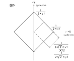
まず、第1発光素子32の配列による解像度を説明する。第1発光素子32は、図3に示すように、X方向にピッチ2×x1で、Y方向にピッチ2×y1で配列されている。したがって、標本化の定理により、第1発光素子32の配列によって復元可能な画像信号の最大周波数は、X方向でR1x=1/(4×x1)と、Y方向でR1y=1/(4×y1)となる。第1発光素子32の配列によって復元可能な画像信号の最大周波数は、第1発光素子32の配列による解像度に相当する。本明細書では、図4に示すように、解像度を、XY平面を用いて表す。図4では、第1発光素子32の配列による解像度は、四角形R1の領域で表される。図4は、四角形の領域が広いほど高解像度であることを示している。
次に、第2発光素子34の配列による解像度を説明する。第2発光素子34は、図3に示すように、X軸方向に対して45°方向にピッチ√2×x1、又はY軸方向に対して45°方向にピッチ√2×y1で配列されている。標本化の定理により、第2発光素子34の配列によって復元可能な画像信号の最大周波数は、X軸方向に対して45°方向又はY軸方向に対して45°方向で、1/(2√2×x1)又は1/(2√2×y1)となる。したがって、第2発光素子34の配列によって復元可能な画像信号の最大周波数は、X方向でR2x=1/(2×x1)と、Y方向でR2y=1/(2×y1)となる。図4では、第2発光素子34の配列による解像度は、四角形R2の領域で表される。
ここで、比較例の表示ユニットの解像度を説明する。比較例の表示ユニットは、第1発光素子32が対角に位置する格子点A、Dのそれぞれに配置され、第2発光素子34が対角に位置する格子点B、Cのそれぞれに配置された画素群を備える。比較例の画素群は、画素群30の格子点Dに第1発光素子32を加えた画素群に相当する。比較例の表示ユニットは、画素群を除き、表示ユニット10と同様である。
比較例の表示ユニットでは、第1発光素子32は、表示ユニット10の第2発光素子34と同様に、X軸方向に対して45°方向にピッチ√2×x1、又はY軸方向に対して45°方向にピッチ√2×y1で配列されている。したがって、比較例において、第1発光素子32の配列によって復元可能な画像信号の最大周波数は、図5に示すように、X軸方向に対して45°方向又はY軸方向に対して45°方向で、1/(2√2×x1)又は1/(2√2×y1)となる。また、比較例の第1発光素子32の配列によって復元可能な画像信号の最大周波数は、X方向で1/(2×x1)と、Y方向で1/(2×y1)となる。比較例の第2発光素子34の配列によって復元可能な画像信号の最大周波数は、比較例の第1発光素子32の配列によって復元可能な画像信号の最大周波数と同様である。
表示ユニット10の解像度と比較例の表示ユニットの解像度とを比較すると、表示ユニット10の色を表現する役割を担う第1発光素子32の解像度は、比較例の表示ユニットの第1発光素子32の解像度に比べて低い。しかしながら、人間の視覚は、明暗の変化に比べて、色の変化に対して鈍感であるので、表示ユニット10の第1発光素子32の解像度の低下は、観察者により認識される画質にほとんど影響しない。すなわち、表示ユニット10では、画質の低下は十分に抑えられている。
さらに、表示ユニット10では、第1発光素子32が画素群30の格子点Dに配置されていないので、表示ユニット10の第1発光素子32の数は、比較例の表示ユニットの第1発光素子32の数に比べて非常に少ない。したがって、表示ユニット10では、発光素子の数を削減して製造コストを低減できる。表示ユニット10では、赤色光と緑色光と青色光とを独立に放射可能で、高価な第1発光素子32の数が少ないので、製造コストを更に低減できる。
以上のように、表示ユニット10では、正方格子30aの格子点Aに第1発光素子32が配置され、正方格子30aの格子点B、Cのそれぞれに第2発光素子34が配置され、正方格子30aの格子点Dに発光素子が配置されないので、発光素子の数を削減して製造コストを低減できる。さらに、表示ユニット10の画質の低下を抑制できる。
<実施形態2>
図6~図8を参照して、実施形態2に係る表示ユニット11を説明する。
実施形態1の表示ユニット10では、画素群30は、正方格子30aの格子点Aと格子点Bとがなす辺を+Y方向に向けて基板20の実装面20aにマトリクス状に配置されている。画素群30は、正方格子30aの辺を、Y軸方向、すなわち鉛直方向に対して45°傾斜した状態で基板20の実装面20aに配置されてもよい。
図6~図8を参照して、実施形態2に係る表示ユニット11を説明する。
実施形態1の表示ユニット10では、画素群30は、正方格子30aの格子点Aと格子点Bとがなす辺を+Y方向に向けて基板20の実装面20aにマトリクス状に配置されている。画素群30は、正方格子30aの辺を、Y軸方向、すなわち鉛直方向に対して45°傾斜した状態で基板20の実装面20aに配置されてもよい。
図6に示すように、表示ユニット11は、実施形態1の表示ユニット10と同様に、基板20と、基板20の実装面20aに配置される複数の画素群30とを備える。表示ユニット11の画素群30は、正方格子30aの辺をY軸方向に対して45°傾け、格子点Aを+Y方向に向けた状態で、基板20の実装面20aに千鳥配列で配置されている。表示ユニット11の画素群30の配列は、表示ユニット10の画素群30の配列を、平面視で左回りに45°回転させた配列に相当する。表示ユニット11は、画素群30の配置を除き、表示ユニット10と同様である。
表示ユニット11の第1発光素子32は、図7に示すように、Y軸方向に対して45°方向にピッチ2×y1で配列されている。したがって、標本化の定理により、表示ユニット11の第1発光素子32の配列によって復元可能な画像信号の最大周波数は、図8に示すように、Y軸に対して45°方向で1/(4×y1)となり、X方向で1/(2√2×x1)と、Y方向で1/(2√2×y1)となる。図8では、表示ユニット11の第1発光素子32の配列による解像度は、四角形R3の領域で表される。
表示ユニット11の第2発光素子34は、図7に示すように、X方向にピッチ√2×x1で、Y方向にピッチ√2×y1で配列されている。したがって、標本化の定理により、表示ユニット11の第2発光素子34の配列によって復元可能な画像信号の最大周波数は、図8に示すように、X方向で1/(2√2×x1)と、Y方向で1/(2√2×y1)となる。図8では、表示ユニット11の第2発光素子34の配列による解像度は、四角形R4の領域で表される。
本実施形態においても、表示ユニット11の色を表現する役割を担う第1発光素子32の解像度は、比較例の表示ユニットの第1発光素子32の解像度に比べて低い。しかしながら、人間の視覚は、明暗の変化に比べて、色の変化に対して鈍感であるので、表示ユニット11の第1発光素子32の解像度の低下は、観察者により認識される画質にほとんど影響しない。さらに、表示ユニット11の第1発光素子32の数は、比較例の表示ユニットの第1発光素子32の数に比べて非常に少ない。したがって、表示ユニット11では、画質の低下を抑えると共に、発光素子の数を削減して製造コストを低減できる。
以上のように、表示ユニット11においても、正方格子30aの格子点Aに第1発光素子32が配置され、正方格子30aの格子点B、Cのそれぞれに第2発光素子34が配置され、正方格子30aの格子点Dに発光素子が配置されないので、画質の低下を抑えると共に製造コストを低減できる。また、表示ユニット11では、図6に示すように、同種の発光素子がX軸方向とY軸方向に並ぶので、表示ユニット11は、正面から外れた位置に位置する観察者に対しても綺麗な表示を実現できる。
<実施形態3>
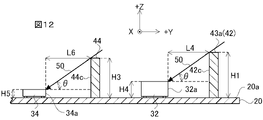
図9~図13を参照して、実施形態3に係る表示ユニット12を説明する。
図9に示すように、表示ユニット12は、実施形態1の表示ユニット10と同様に、基板20と、基板20の実装面20aに配置される複数の画素群30とを備える。表示ユニット12は、外光50を遮る第1庇部42と第2庇部44とを更に備える。外光50は、太陽光と照明とを含む、表示ユニット12の周囲から表示ユニット12に入射する光を意味する。外光50を遮るとは、第1発光素子32と第2発光素子34と基板20の実装面20aへの外光50の入射を抑制することを意味する。表示ユニット12の基板20と画素群30は、表示ユニット10の基板20と画素群30と同様である。
第1庇部42は、X軸方向に延びる黒色の板である。第1庇部42は、例えば、黒色の樹脂から射出成形によって作製される。第1庇部42は、基板20の実装面20aの上に設けられる。第1庇部42は、例えば、基板20の実装面20aに対向する面からネジ止めされることによって、基板20の実装面20aに固定される。第1庇部42は、表示ユニット12を設置した状態において、X軸方向に延びる第1発光素子32と第2発光素子34の列の鉛直上方、すなわちX軸方向に延びる第1発光素子32と第2発光素子34の列の+Y方向側に配置される。
第1庇部42は、図10に示すように、基板20の実装面20aから上端までの高さが異なる段差を、上面42aに有している。第1庇部42のX軸方向の長さL2は、基板20のX軸方向の長さL1と等しい。また、第1庇部42のY軸方向の長さD1は、正方格子30aの間隔y1よりも狭く設定される。第1庇部42の実装面20aから上端までの高さH1、H2については、後述する。第1庇部42の実装面20aから上端までの高さは、第1庇部42のZ軸方向の長さを指す。また、第1庇部42の表示ユニット12の正面側に配置される面を上面42aと、第1庇部42の実装面20aに垂直な面を側面とする。
第2庇部44は、図11に示すように、X軸方向に延びる黒色の板である。第2庇部44は、例えば、黒色の樹脂から射出成形によって作製される。第2庇部44は、第1庇部42と同様に、基板20の実装面20aに対向する面からネジ止めされることによって、基板20の実装面20aの上に設けられる。第2庇部44は、表示ユニット12を設置した状態において、X軸方向に延びる第2発光素子34の列の鉛直上方、すなわちX軸方向に延びる第2発光素子34の列の+Y方向側に配置される。
第2庇部44のX軸方向の長さL3は、基板20のX軸方向の長さL1と等しい。また、第2庇部44のY軸方向の長さD2は、正方格子30aの間隔y1よりも狭く設定される。第2庇部44の基板20の実装面20aから上端までの高さH3については、後述する。第2庇部44の基板20の実装面20aから上端までの高さH3は、第2庇部44のZ軸方向の長さを指す。また、第2庇部44の表示ユニット12の正面側に配置される面を上面と、第2庇部44の実装面20aに垂直な面を側面とする。
本実施形態では、第1庇部42と第2庇部44は、Y軸方向に等間隔で配列されている。
本実施形態では、第1庇部42と第2庇部44は、Y軸方向に等間隔で配列されている。
第1庇部42の高さH1、H2について説明する。本実施形態では、第1発光素子32の基板20の実装面20aから上端までの高さH4が、第2発光素子34の基板20の実装面20aから上端までの高さH5よりも高いと仮定する。第1発光素子32の基板20の実装面20aから上端までの高さH4は、第1発光素子32のZ軸方向の長さを指す。第2発光素子34の基板20の実装面20aから上端までの高さH5は、第2発光素子34のZ軸方向の長さを指す。
図9に示すように、第1庇部42の実装面20aから上端までの高さが高い部分43aは、表示ユニット12を設置した状態において、第1発光素子32の鉛直上方に位置している。また、第1庇部42の実装面20aから上端までの高さが低い部分43bは、表示ユニット12を設置した状態において、第2発光素子34の鉛直上方に位置している。
第1庇部42の部分43aの高さH1は、図12に示すように、第1発光素子32の高さH4と、第1発光素子32と第1庇部42の部分43aとの距離とに応じて設定される。具体的には、表示ユニット12を設置した状態において、第1庇部42が鉛直上方に対して入射角θよりも小さい入射角の外光50を遮る場合、第1発光素子の高さH4と、第1発光素子32の第1庇部42側の側面32aと第1庇部42の部分43aの第1発光素子32側の側面42cとの距離L4から、第1庇部42の部分43aの高さH1はH1=H4+L4×tanθに設定される。
第1庇部42の部分43bの高さH2は、図13に示すように、第2発光素子34の高さH5と、第2発光素子34と第1庇部42の部分43bとの距離とに応じて設定される。具体的には、表示ユニット12を設置した状態において、鉛直上方に対して入射角θよりも小さい外光50を遮る場合、第2発光素子34の高さH5と、第2発光素子34の第1庇部42側の側面34aと第1庇部42の部分43bの第2発光素子34側の側面42cとの距離L5から、第1庇部42の部分43bの高さH2はH2=H5+L5×tanθに設定される。
次に、第2庇部44の高さH3について説明する。第2庇部44の高さH3は、図12に示すように、第2発光素子34の高さH5と、第2発光素子34と第2庇部44との距離とに応じて設定される。具体的には、表示ユニット12を設置した状態において、第2庇部44が鉛直上方に対して入射角θよりも小さい外光50を遮る場合、第2発光素子34の高さH5と、第2発光素子34の第2庇部44側の側面34aと第2庇部44の第2発光素子34側の側面44cとの距離L6から、第2庇部44の高さH3はH3=H5+L6×tanθに設定される。
本実施形態では、第1発光素子32の高さH4が第2発光素子34の高さH5よりも高い。したがって、距離L4と距離L5と距離L6が等しければ、第1庇部42の部分43aの高さH1は、第1庇部42の部分43bの高さH2又は第2庇部44の高さH3よりも、第1発光素子32の高さH4と第2発光素子34の高さH5との差分だけ高く設定される。
本実施形態では、第1発光素子32の高さH4が第2発光素子34の高さH5よりも高い。したがって、距離L4と距離L5と距離L6が等しければ、第1庇部42の部分43aの高さH1は、第1庇部42の部分43bの高さH2又は第2庇部44の高さH3よりも、第1発光素子32の高さH4と第2発光素子34の高さH5との差分だけ高く設定される。
本実施形態では、第1庇部42の高さH1、H2と第2庇部44の高さH3が、第1発光素子32の高さH4と第2発光素子34の高さH5と、第1発光素子32と第1庇部42との距離L4と、第2発光素子34と第1庇部42又は第2庇部44との距離L5、L6とに応じて設定される。これにより、第1発光素子32と第2発光素子34と基板20の実装面20aに入射する外光50を表示ユニット12全体に渡って均一に遮ることができる。外光50を均一に遮ることにより、表示ユニット12はムラのない表示を実現できる。さらに、第1庇部42の高さH1、H2と第2庇部44の高さH3を、第1発光素子32の高さH4と第2発光素子34の高さH5のそれぞれに適した高さに設定できるので、表示ユニット12は、第1発光素子32と第2発光素子34による外光50の反射をより効果的に抑制して、コントラストの高い表示を実現できる。
以上のように、表示ユニット12は、第1発光素子32の高さH4と第2発光素子34の高さH5と、第1発光素子32又は第2発光素子34との距離とに応じた高さを有する第1庇部42と第2庇部44を備えるので、均一に外光50を遮り、ムラのない表示を実現できる。さらに、表示ユニット12は、コントラストの高い表示を実現できる。表示ユニット12は、実施形態1の表示ユニット10と同様に、画質の低下を抑えると共に製造コストを低減できる。
<実施形態4>
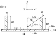
図14~図18を参照して、実施形態4に係る表示ユニット13を説明する。
図14に示すように、表示ユニット13は、実施形態2の表示ユニット11と同様に、基板20と、基板20の実装面20aに配置される複数の画素群30とを備える。また、表示ユニット13は、基板20の実装面20aに、外光50を遮る第3庇部46と第4庇部48とを備える。表示ユニット13の基板20と画素群30は、表示ユニット11の基板20と画素群30と同様である。本実施形態においても、第3庇部46と第4庇部48の表示ユニット13の正面側に配置される面を上面と、第3庇部46と第4庇部48の実装面20aに垂直な面を側面とする。また、第3庇部46の基板20の実装面20aから上端までの高さH6は第3庇部46のZ軸方向の長さを、第4庇部48の基板20の実装面20aから上端までの高さH7は第4庇部48のZ軸方向の長さを指す。
第3庇部46は、図15に示すように、X軸方向に延びる黒色の板である。また、第4庇部48は、図16に示すように、X軸方向に延びる黒色の板である。第3庇部46と第4庇部48は、第2庇部44と同様に、黒色の樹脂から射出成形によって作製される。図14に示すように、第3庇部46は、表示ユニット13を設置した状態において、X軸方向に延びる第1発光素子32の列の鉛直上方に配置される。第4庇部48は、表示ユニット13を設置した状態において、X軸方向に延びる第2発光素子34の列の鉛直上方に配置される。
第3庇部46と第4庇部48は、第2庇部44と同様に、基板20の実装面20aに対向する面からネジ止めされることによって、基板20の実装面20aの上に設けられる。
第3庇部46と第4庇部48は、第2庇部44と同様に、基板20の実装面20aに対向する面からネジ止めされることによって、基板20の実装面20aの上に設けられる。
第3庇部46のX軸方向の長さL7と第4庇部48のX軸方向の長さL8は、基板20のX軸方向の長さL1と等しい。また、第3庇部46のY軸方向の長さD3と第4庇部48のY軸方向の長さD4は、正方格子30aの間隔y1よりも狭く設定される。第3庇部46の高さH6と第4庇部48の高さH7については、後述する。
第3庇部46の高さH6と第4庇部48の高さH7を説明する。本実施形態においても、第1発光素子32の高さH4が、第2発光素子34の高さH5よりも高いと仮定する。
第3庇部46の高さH6は、図17に示すように、第1発光素子32の高さH4と、第1発光素子32と第3庇部46との距離とに応じて設定される。具体的には、表示ユニット13を設置した状態において、第3庇部46が鉛直上方に対して入射角φよりも小さい外光50を遮る場合、第1発光素子32の高さH4と、第1発光素子32の第3庇部46側の側面32aと第3庇部46の第1発光素子32側の側面46cとの距離L9から、第3庇部46の高さH6はH6=H4+L9×tanφに設定される。
第4庇部48の高さH7は、図18に示すように、第2発光素子34の高さH5と、第2発光素子34と第4庇部48との距離とに応じて設定される。具体的には、表示ユニット13を設置した状態において、第4庇部48が鉛直上方に対して入射角φよりも小さい外光50を遮る場合、第2発光素子34の高さH5と、第2発光素子34の第4庇部48側の側面34aと第4庇部48の第2発光素子34側の側面48cとの距離L10から、第4庇部48の高さH7はH7=H5+L10×tanφに設定される。
本実施形態においても、第1発光素子32の高さH4が第2発光素子34の高さH5よりも高い。したがって、距離L9と距離L10が等しければ、第3庇部46の高さH6は、第4庇部48の高さH7よりも、第1発光素子32の高さH4と第2発光素子34の高さH5との差分だけ高く設定される。
本実施形態においても、第1発光素子32の高さH4が第2発光素子34の高さH5よりも高い。したがって、距離L9と距離L10が等しければ、第3庇部46の高さH6は、第4庇部48の高さH7よりも、第1発光素子32の高さH4と第2発光素子34の高さH5との差分だけ高く設定される。
第3庇部46の高さH6と第4庇部48の高さH7が、第1発光素子32の高さH4と第2発光素子34の高さH5と、第1発光素子32又は第2発光素子34との距離とに応じた高さに設定されるので、表示ユニット13は、実施形態3の表示ユニット12と同様に、ムラのない表示を実現できる。また、表示ユニット13は、実施形態3の表示ユニット12と同様に、コントラストの高い表示を実現できる。さらに、第3庇部46と第4庇部48は、上面に、実施形態3の第1庇部42の上面42aに設けられている段差を有していないので、表示ユニット13は、ざらつき感のない滑らかな表示を実現できる。
以上のように、表示ユニット13は、均一に外光を遮り、ムラのない表示を実現できる。また、表示ユニット13はコントラストの高い表示を実現できる。さらに、第3庇部46と第4庇部48が上面に段差を有していないので、表示ユニット13はざらつき感のない滑らかな表示を実現できる。表示ユニット13は、実施形態2の表示ユニット11と同様に、画質の低下を抑えると共に製造コストを低減できる。
<実施形態5>
図19~図22を参照して、実施形態5に係る表示ユニット14を説明する。
図19に示すように、表示ユニット14は、実施形態2の表示ユニット11と同様に、基板20と、基板20の実装面20aに配置される複数の画素群30とを備える。表示ユニット14は、外光50を遮るマスク板60を更に備える。マスク板60は、図19、図20に示すように、第1発光素子32と第2発光素子34のそれぞれを挿入される複数の開口部62と開口部64とを有する。表示ユニット14の基板20と画素群30は、表示ユニット11の基板20と画素群30と同様である。
図19~図22を参照して、実施形態5に係る表示ユニット14を説明する。
図19に示すように、表示ユニット14は、実施形態2の表示ユニット11と同様に、基板20と、基板20の実装面20aに配置される複数の画素群30とを備える。表示ユニット14は、外光50を遮るマスク板60を更に備える。マスク板60は、図19、図20に示すように、第1発光素子32と第2発光素子34のそれぞれを挿入される複数の開口部62と開口部64とを有する。表示ユニット14の基板20と画素群30は、表示ユニット11の基板20と画素群30と同様である。
マスク板60は黒色の板である。マスク板60は、例えば、黒色の樹脂から射出成形によって作製される。図19に示すように、マスク板60のX軸方向の長さL11は基板20のX軸方向の長さL1と等しく、マスク板60のY軸方向の長さL12は基板20のX軸方向の長さL13と等しい。
マスク板60は、第1発光素子32が基板20の実装面20aに実装されている位置に開口部62を有する。また、マスク板60は、第2発光素子34が基板20の実装面20aに実装されている位置に開口部64を有する。開口部62、64は矩形状に形成される。開口部62と開口部64のそれぞれには、第1発光素子32と第2発光素子34のそれぞれが挿入される。開口部62、64の平面サイズについては、後述する。平面サイズは、表示ユニット14を平面視した場合の大きさを意味する。
マスク板60は、第1発光素子32が開口部62に挿入され、第2発光素子34が開口部64に挿入された状態で、基板20の実装面20aに配置される。マスク板60は、例えば、基板20の実装面20aに対向する面から基板20にネジ止めされる。
開口部62、64の平面サイズについて説明する。本実施形態では、第1発光素子32の上面33の平面サイズが、第2発光素子34の上面35の平面サイズよりも大きいと仮定する。また、第1発光素子32の上面33のX軸方向の長さをUL1、第1発光素子32の上面33のY軸方向の長さをUL2とする。第2発光素子34の上面35のX軸方向の長さをUL3、第2発光素子34の上面35のY軸方向の長さをUL4とする。ここでは、UL1>UL3、UL2>UL4である。さらに、開口部62のX軸方向の長さをML1、開口部62のY軸方向の長さをML2とする。開口部64のX軸方向の長さをML3、開口部62のY軸方向の長さをML4とする。
開口部62の平面サイズは、第1発光素子32の平面サイズに応じて設定され、第1発光素子32の平面サイズよりもわずかに大きい。例えば、平面視において、開口部62の中心P1と第1発光素子32の上面33の中心P2が一致している場合、図21に示すように、開口部62と第1発光素子32との間に、X軸方向で長さGL1、Y軸方向で長さGL2の隙間が設けられる。X軸方向の隙間の長さGL1はGL1=(ML1-UL1)/2であり、Y軸方向の隙間の長さGL2はGL2=(ML2-UL2)/2である。隙間の長さGL1、GL2は、例えば、100μm~500μmである。
開口部64の平面サイズは、第2発光素子34の平面サイズに応じて設定され、第2発光素子34の平面サイズよりもわずかに大きい。平面視において、開口部64の中心P3と第2発光素子34の上面33の中心P4が一致している場合、図22に示すように、X軸方向で長さGL3=(ML3-UL3)/2、Y軸方向で長さGL4=(ML4-UL4)/2の隙間が、開口部64と第2発光素子34との間に設けられる。隙間の長さGL3、GL4は、例えば、100μm~500μmである。
本実施形態では、第1発光素子32の上面33の平面サイズが、第2発光素子34の上面35の平面サイズよりも大きい。したがって、開口部62の平面サイズは、開口部64の平面サイズよりも大きく設定される。
本実施形態では、第1発光素子32の上面33の平面サイズが、第2発光素子34の上面35の平面サイズよりも大きい。したがって、開口部62の平面サイズは、開口部64の平面サイズよりも大きく設定される。
本実施形態では、開口部62の平面サイズと開口部64の平面サイズのそれぞれを、第1発光素子32の上面33の平面サイズと第2発光素子34の上面35の平面サイズのそれぞれに適したサイズに設定できるので、表示ユニット14は、第1発光素子32と第2発光素子34と実装面20aによる外光50の反射をより効果的に抑制して、コントラストの高い表示を実現できる。また、図19に示すように、同じ平面サイズの開口部62、64がX軸方向とY軸方向に並ぶので、表示ユニット14は滑らかな表示を実現できる。
開口部62におけるX軸方向の隙間の長さGL1と開口部64におけるX軸方向の隙間の長さGL3は等しいことが、好ましい。また、開口部62におけるY軸方向の隙間の長さGL2と開口部64におけるY軸方向の隙間の長さGL4は等しいことが、好ましい。これらにより、表示ユニット14は、より均一でより滑らかな表示を実現できる。
以上のように、表示ユニット14では、マスク板60が第1発光素子32の平面サイズと第2発光素子34の平面サイズのそれぞれに応じた平面サイズを有する開口部62と開口部64を有するので、表示ユニット14はコントラストの高い表示を実現できる。また、表示ユニット14では、同じ平面サイズの開口部62、64がX軸方向とY軸方向に並ぶので、表示ユニット14は滑らかな表示を実現できる。さらに、表示ユニット14は、実施形態2の表示ユニット11と同様に、画質の低下を抑えると共に製造コストを低減できる。
<実施形態6>
図23を参照して、実施形態6に係る表示装置15を説明する。
複数の表示ユニット10~14を組み合わせることによって、より大型の表示装置15を形成できる。表示装置15は、競技場、ビルの壁面等の野外に設置される。
図23を参照して、実施形態6に係る表示装置15を説明する。
複数の表示ユニット10~14を組み合わせることによって、より大型の表示装置15を形成できる。表示装置15は、競技場、ビルの壁面等の野外に設置される。
図23に示すように、表示装置15は、例えば、12個の表示ユニット13と、12個の表示ユニット13を収納する筐体80とを備える。
12個の表示ユニット13は、4行×3列に配列される。配列された表示ユニット13は、筐体80に収納される。表示ユニット13は、例えば、筐体80にネジ止めされる。筐体80は、例えば、金属製の箱型の筐体である。
表示装置15は、表示ユニット13と同様に、ムラのない表示を実現できる。また、表示装置15はコントラストの高い表示を実現できる。さらに、表示装置15は、ざらつき感のない滑らかな表示を実現できる。表示装置15は、画質の低下を抑えると共に製造コストを低減できる。
<変形例>
以上、複数の実施形態を説明したが、本開示は、上記の実施形態に限定されず、本開示の要旨を逸脱しない範囲で種々の変更が可能である。
以上、複数の実施形態を説明したが、本開示は、上記の実施形態に限定されず、本開示の要旨を逸脱しない範囲で種々の変更が可能である。
例えば、第1発光素子32と第2発光素子34はLED素子に限られない。第1発光素子32と第2発光素子34はレーザダイオード(LD:Laser Diode)素子であってもよい。また、LED素子は、表面実装型LED素子に限られず、砲弾型LED素子であってもよい。
白色光のみを放射する第2発光素子34は、図24に示すように、放射光を集光するレンズ部38を備えてもよい。第2発光素子34から放射される白色光を集光することにより、表示ユニット10~14と表示装置15は、高輝度の表示を実現でき、くっきりした文字、画像等を提供できる。
赤色光と緑色光と青色光とを独立に放射可能である第1発光素子32も、放射光を集光するレンズ部38を備えてもよい。第1発光素子32の放射光が集光され過ぎると、観察者が色分離した画像を認識してしまうので、第1発光素子32と第2発光素子34がレンズ部38を備える場合、第1発光素子32のレンズ部38の曲率は、第2発光素子34のレンズ部38の曲率よりも小さいことが好ましい。
実施形態1の表示ユニット10では、画素群30は、格子点Aと格子点Bとがなす辺を上方に向けて配置されている。また、実施形態2の表示ユニット11では、画素群30は、格子点Aを上方に向けて配置されている。画素群30の配置される向きは、任意である。例えば、画素群30は格子点Aを鉛直下方に向けて配置されてもよい。
実施形態3と実施形態4では、第1発光素子32の高さH4が第2発光素子34の高さH5よりも高いと仮定したが、第2発光素子34の高さH5が第1発光素子32の高さH4よりも高くともよい。例えば、実施形態4において、第2発光素子34の高さH5が第1発光素子32の高さH4よりも高く、距離L9と距離L10が等しければ、第4庇部48の高さH7は、第3庇部46の高さH6よりも、第2発光素子34の高さH5と第1発光素子32の高さH4との差分だけ高く設定される。
実施形態5では、第1発光素子32の上面33の平面サイズが第2発光素子34の上面35の平面サイズよりも大きいと仮定したが、第2発光素子34の上面35の平面サイズが第1発光素子32の上面33の平面サイズよりも大きくともよい。例えば、第2発光素子34の上面35の平面サイズが第1発光素子32の上面33の平面サイズよりも大きい場合、マスク板60の開口部64の平面サイズは、マスク板60の開口部62の平面サイズよりも大きく設定される。
実施形態1の表示ユニット10は、実施形態5の表示ユニット14と同様に、マスク板を備えてもよい。
また、実施形態3の表示ユニット12と実施形態4の表示ユニット13は、実施形態5の表示ユニット14と同様に、マスク板を備えてもよい。この場合、表示ユニット12の第1庇部42と第2庇部44はマスク板の上に設けられる。第1庇部42と第2庇部44とマスク板は一体に形成されてもよい。また、表示ユニット13の第3庇部46と第4庇部48はマスク板60の上に設けられる。第3庇部46と第4庇部48とマスク板60は、一体に形成されてもよい。
実施形態1~実施形態5では、第1発光素子32が赤色光と緑色光と青色光とを独立に放射可能であり、第2発光素子34が白色光のみを放射する。表示ユニット10~14では、第2発光素子34が赤色光と緑色光と青色光とを独立に放射可能であり、第1発光素子32が白色光のみを放射してもよい。すなわち、第1発光素子32と第2発光素子34のうちの一方が赤色光と緑色光と青色光とを独立に放射可能であり、第1発光素子32と第2発光素子34のうちの他方が白色光のみを放射すればよい。第2発光素子34が赤色光と緑色光と青色光とを独立に放射可能であり、第1発光素子32が白色光のみを放射する場合であっても、画質の低下を抑えると共に、発光素子の数を削減して製造コストを低減できる。
表示装置15は、表示ユニット13に代えて、表示ユニット10~12、14を備えてもよい。表示装置15を形成する表示ユニット10~14の数と配列は、任意である。表示ユニット10~14と表示装置15は、屋外に限られず、体育館、室内プール等の屋内に設置されてもよい。
10,11,12,13,14 表示ユニット、15 表示装置、20 基板、20a 実装面、30 画素群、30a 正方格子、32 第1発光素子、32a 第1発光素子の側面、33 第1発光素子の上面、34 第2発光素子、34a 第2発光素子の側面、35 第2発光素子の上面、38 レンズ部、42 第1庇部、42a 第1庇部の上面、42c 第1庇部の側面、43a,43b 第1庇部の部分、44 第2庇部、44c 第2庇部の側面、46 第3庇部、46c 第3庇部の側面、48 第4庇部、48c 第4庇部の側面、50 外光、60 マスク板、62,64 開口部、80 筐体、x1,y1 間隔(画素ピッチ)、A,B,C,D 格子点、D1,D2,D3,D4,L1,L2,L3,L7,L8,L11,L12,L13,ML1,ML2,ML3,ML4,UL1,UL2,UL3,UL4,GL1,GL2,GL3,GL4 長さ、L4,L5,L6,L9,L10 距離、H1,H2,H3,H4,H5,H6,H7 高さ、P1,P2,P3,P4 中心、R1,R2,R3,R4 四角形、θ,φ 入射角
Claims (10)
- 基板と、
前記基板の実装面に配置され、正方格子の3つの格子点に画素を有し、前記正方格子の残りの格子点に画素を有さない複数の画素群と、を備え、
前記画素群は、画素として、前記正方格子の格子点の1つに位置する第1発光素子と、前記第1発光素子が位置する前記正方格子の格子点に隣り合う2つの前記正方格子の格子点のそれぞれに位置する第2発光素子とを有し、
前記第1発光素子と前記第2発光素子のうちの一方は、赤色光と緑色光と青色光とを独立に放射可能であり、前記第1発光素子と前記第2発光素子のうちの他方は、白色光のみを放射する、
表示ユニット。 - 設置した状態において、前記正方格子の辺が鉛直方向に対して45°傾斜している、
請求項1に記載の表示ユニット。 - 前記画素の列の方向に沿って延びる庇部を備える、
請求項1又は2に記載の表示ユニット。 - 設置した状態において、前記第1発光素子の鉛直上方に位置する前記庇部と前記第2発光素子の鉛直上方に位置する前記庇部は、それぞれ、前記第1発光素子の前記実装面からの高さと前記第2発光素子の前記実装面からの高さに応じた、前記実装面からの高さを有する、
請求項3に記載の表示ユニット。 - 設置した状態において、赤色光と緑色光と青色光とを独立に放射可能である前記第1発光素子又は前記第2発光素子の鉛直上方に位置する前記庇部の前記実装面からの高さが、白色光のみを放射する前記第1発光素子又は前記第2発光素子の鉛直上方に位置する前記庇部の前記実装面からの高さよりも、高い、
請求項3又は4に記載の表示ユニット。 - 前記第1発光素子が実装された位置と前記第2発光素子が実装された位置に形成され、前記第1発光素子と前記第2発光素子のそれぞれを挿入される複数の開口部を有し、前記実装面に配置されるマスク板を、備える、
請求項1から5のいずれか1項に記載の表示ユニット。 - 前記第1発光素子を挿入される前記開口部と前記第2発光素子を挿入される前記開口部は、それぞれ、前記第1発光素子の大きさと前記第2発光素子の大きさに応じた大きさを有する、
請求項6に記載の表示ユニット。 - 前記第1発光素子を挿入される前記開口部と前記第1発光素子との間の隙間の大きさと、前記第2発光素子を挿入される前記開口部と前記第2発光素子との間の隙間の大きさとが、等しい、
請求項6又は7に記載の表示ユニット。 - 白色光のみを放射する前記第1発光素子又は前記第2発光素子は、放射光を集光するレンズ部を有する、
請求項1から8のいずれか1項に記載の表示ユニット。 - 請求項1から9のいずれか1項に記載の表示ユニットを複数組み合わされた、表示装置。
Priority Applications (2)
| Application Number | Priority Date | Filing Date | Title |
|---|---|---|---|
| JP2022581047A JP7395033B2 (ja) | 2021-02-09 | 2021-02-09 | 表示ユニット及び表示装置 |
| PCT/JP2021/004773 WO2022172324A1 (ja) | 2021-02-09 | 2021-02-09 | 表示ユニット及び表示装置 |
Applications Claiming Priority (1)
| Application Number | Priority Date | Filing Date | Title |
|---|---|---|---|
| PCT/JP2021/004773 WO2022172324A1 (ja) | 2021-02-09 | 2021-02-09 | 表示ユニット及び表示装置 |
Publications (1)
| Publication Number | Publication Date |
|---|---|
| WO2022172324A1 true WO2022172324A1 (ja) | 2022-08-18 |
Family
ID=82838447
Family Applications (1)
| Application Number | Title | Priority Date | Filing Date |
|---|---|---|---|
| PCT/JP2021/004773 WO2022172324A1 (ja) | 2021-02-09 | 2021-02-09 | 表示ユニット及び表示装置 |
Country Status (2)
| Country | Link |
|---|---|
| JP (1) | JP7395033B2 (ja) |
| WO (1) | WO2022172324A1 (ja) |
Citations (6)
| Publication number | Priority date | Publication date | Assignee | Title |
|---|---|---|---|---|
| JPH10161569A (ja) * | 1996-11-26 | 1998-06-19 | Takiron Co Ltd | Ledドットマトリクス発光表示体 |
| JPH10254386A (ja) * | 1997-03-14 | 1998-09-25 | Sony Corp | カラー画像表示装置 |
| JP2003255862A (ja) * | 2002-02-28 | 2003-09-10 | Matsushita Electric Ind Co Ltd | ディスプレイモジュールおよびこれを用いた表示装置 |
| JP2009230096A (ja) * | 2008-02-25 | 2009-10-08 | Mitsubishi Electric Corp | 画像表示装置及び画像表示装置用表示ユニット |
| JP2015111288A (ja) * | 2011-12-27 | 2015-06-18 | 三菱電機株式会社 | 表示装置 |
| WO2018138892A1 (ja) * | 2017-01-27 | 2018-08-02 | 三菱電機株式会社 | 表示ユニット、表示装置及び表示ユニットの製造方法 |
-
2021
- 2021-02-09 WO PCT/JP2021/004773 patent/WO2022172324A1/ja active Application Filing
- 2021-02-09 JP JP2022581047A patent/JP7395033B2/ja active Active
Patent Citations (6)
| Publication number | Priority date | Publication date | Assignee | Title |
|---|---|---|---|---|
| JPH10161569A (ja) * | 1996-11-26 | 1998-06-19 | Takiron Co Ltd | Ledドットマトリクス発光表示体 |
| JPH10254386A (ja) * | 1997-03-14 | 1998-09-25 | Sony Corp | カラー画像表示装置 |
| JP2003255862A (ja) * | 2002-02-28 | 2003-09-10 | Matsushita Electric Ind Co Ltd | ディスプレイモジュールおよびこれを用いた表示装置 |
| JP2009230096A (ja) * | 2008-02-25 | 2009-10-08 | Mitsubishi Electric Corp | 画像表示装置及び画像表示装置用表示ユニット |
| JP2015111288A (ja) * | 2011-12-27 | 2015-06-18 | 三菱電機株式会社 | 表示装置 |
| WO2018138892A1 (ja) * | 2017-01-27 | 2018-08-02 | 三菱電機株式会社 | 表示ユニット、表示装置及び表示ユニットの製造方法 |
Also Published As
| Publication number | Publication date |
|---|---|
| JPWO2022172324A1 (ja) | 2022-08-18 |
| JP7395033B2 (ja) | 2023-12-08 |
Similar Documents
| Publication | Publication Date | Title |
|---|---|---|
| US10468391B2 (en) | Inorganic light-emitting-diode displays with multi-ILED pixels | |
| KR102146961B1 (ko) | 픽셀 구조와 그의 디스플레이 방법, 및 디스플레이 디바이스 | |
| US20200258441A1 (en) | Sub-pixel arrangement structure, mask device, and display device | |
| CN114994973B (zh) | 显示基板和显示装置 | |
| US10396062B2 (en) | Micro light emitting diode display panel | |
| JP2022514274A (ja) | 表示基板、表示パネル及び表示装置 | |
| US11211430B2 (en) | Display panel for improving display effect in low-resolution area, manufacturing method thereof, and display device | |
| WO2019019604A1 (zh) | 显示基板、显示装置及其显示方法、掩模板 | |
| KR102238284B1 (ko) | 능동화소 ic를 포함하는 led 픽셀 패키지 및 그 제조방법 | |
| WO2019153939A1 (zh) | 像素排列结构、显示基板、显示装置和掩摸板 | |
| US20230142473A1 (en) | Display panel and manufacturing method therefor, and display device | |
| US6892014B2 (en) | Display device having a fiber optic faceplate | |
| JP6355445B2 (ja) | 映像表示装置、大型表示装置及び映像表示装置の製造方法 | |
| KR100495719B1 (ko) | 화상표시장치및그화소배열방법 | |
| CN215578617U (zh) | 一种显示面板和显示装置 | |
| KR20150106622A (ko) | 유기 발광 표시 장치 | |
| WO2022172324A1 (ja) | 表示ユニット及び表示装置 | |
| US11152423B2 (en) | Optical assembly and display device comprising an arrangement of luminescence diode chips | |
| CN111490039B (zh) | 发光二极管显示面板 | |
| US20230044657A1 (en) | Surface Mount Devices Containing a Plurality of Pixels and Sub-Pixels and Providing Off-Axis Color Correction for Video Wall Displays | |
| CN110780364A (zh) | 光控膜和包括该光控膜的显示装置 | |
| JP2004184669A (ja) | Ledユニット | |
| JP7045951B2 (ja) | 表示ユニット及び表示装置 | |
| CN115699309A (zh) | 包括低亮度区域的显示装置 | |
| KR20170139364A (ko) | 발광소자 패키지 및 이를 포함하는 표시장치 |
Legal Events
| Date | Code | Title | Description |
|---|---|---|---|
| 121 | Ep: the epo has been informed by wipo that ep was designated in this application |
Ref document number: 21925578 Country of ref document: EP Kind code of ref document: A1 |
|
| ENP | Entry into the national phase |
Ref document number: 2022581047 Country of ref document: JP Kind code of ref document: A |
|
| NENP | Non-entry into the national phase |
Ref country code: DE |
|
| 122 | Ep: pct application non-entry in european phase |
Ref document number: 21925578 Country of ref document: EP Kind code of ref document: A1 |