WO2022158278A1 - 撮像素子、撮像装置 - Google Patents
撮像素子、撮像装置 Download PDFInfo
- Publication number
- WO2022158278A1 WO2022158278A1 PCT/JP2021/048958 JP2021048958W WO2022158278A1 WO 2022158278 A1 WO2022158278 A1 WO 2022158278A1 JP 2021048958 W JP2021048958 W JP 2021048958W WO 2022158278 A1 WO2022158278 A1 WO 2022158278A1
- Authority
- WO
- WIPO (PCT)
- Prior art keywords
- detection
- region
- imaging device
- substrate
- elements
- Prior art date
- Legal status (The legal status is an assumption and is not a legal conclusion. Google has not performed a legal analysis and makes no representation as to the accuracy of the status listed.)
- Ceased
Links
Images






Classifications
-
- H—ELECTRICITY
- H04—ELECTRIC COMMUNICATION TECHNIQUE
- H04N—PICTORIAL COMMUNICATION, e.g. TELEVISION
- H04N25/00—Circuitry of solid-state image sensors [SSIS]; Control thereof
- H04N25/70—SSIS architectures; Circuits associated therewith
- H04N25/76—Addressed sensors, e.g. MOS or CMOS sensors
- H04N25/77—Pixel circuitry, e.g. memories, A/D converters, pixel amplifiers, shared circuits or shared components
-
- H—ELECTRICITY
- H04—ELECTRIC COMMUNICATION TECHNIQUE
- H04N—PICTORIAL COMMUNICATION, e.g. TELEVISION
- H04N25/00—Circuitry of solid-state image sensors [SSIS]; Control thereof
- H04N25/47—Image sensors with pixel address output; Event-driven image sensors; Selection of pixels to be read out based on image data
-
- H—ELECTRICITY
- H04—ELECTRIC COMMUNICATION TECHNIQUE
- H04N—PICTORIAL COMMUNICATION, e.g. TELEVISION
- H04N25/00—Circuitry of solid-state image sensors [SSIS]; Control thereof
- H04N25/70—SSIS architectures; Circuits associated therewith
- H04N25/76—Addressed sensors, e.g. MOS or CMOS sensors
- H04N25/78—Readout circuits for addressed sensors, e.g. output amplifiers or A/D converters
-
- H—ELECTRICITY
- H04—ELECTRIC COMMUNICATION TECHNIQUE
- H04N—PICTORIAL COMMUNICATION, e.g. TELEVISION
- H04N25/00—Circuitry of solid-state image sensors [SSIS]; Control thereof
- H04N25/70—SSIS architectures; Circuits associated therewith
- H04N25/79—Arrangements of circuitry being divided between different or multiple substrates, chips or circuit boards, e.g. stacked image sensors
-
- H—ELECTRICITY
- H10—SEMICONDUCTOR DEVICES; ELECTRIC SOLID-STATE DEVICES NOT OTHERWISE PROVIDED FOR
- H10F—INORGANIC SEMICONDUCTOR DEVICES SENSITIVE TO INFRARED RADIATION, LIGHT, ELECTROMAGNETIC RADIATION OF SHORTER WAVELENGTH OR CORPUSCULAR RADIATION
- H10F39/00—Integrated devices, or assemblies of multiple devices, comprising at least one element covered by group H10F30/00, e.g. radiation detectors comprising photodiode arrays
- H10F39/80—Constructional details of image sensors
- H10F39/803—Pixels having integrated switching, control, storage or amplification elements
- H10F39/8037—Pixels having integrated switching, control, storage or amplification elements the integrated elements comprising a transistor
-
- H—ELECTRICITY
- H10—SEMICONDUCTOR DEVICES; ELECTRIC SOLID-STATE DEVICES NOT OTHERWISE PROVIDED FOR
- H10F—INORGANIC SEMICONDUCTOR DEVICES SENSITIVE TO INFRARED RADIATION, LIGHT, ELECTROMAGNETIC RADIATION OF SHORTER WAVELENGTH OR CORPUSCULAR RADIATION
- H10F39/00—Integrated devices, or assemblies of multiple devices, comprising at least one element covered by group H10F30/00, e.g. radiation detectors comprising photodiode arrays
- H10F39/80—Constructional details of image sensors
- H10F39/809—Constructional details of image sensors of hybrid image sensors
Definitions
- the present technology relates to an image pickup device and an image pickup device, and for example, an image pickup device and an image pickup device that compare the amount of change in brightness with a threshold.
- a synchronous imaging device that captures image data (frames) in synchronization with a synchronization signal such as a vertical synchronization signal is used.
- This general synchronous imaging device can only acquire image data at each synchronization signal cycle (e.g., 1/60th of a second). It becomes difficult to respond when Therefore, an asynchronous imaging device has been proposed that detects, as an address event, that the amount of change in luminance of a pixel exceeds a threshold value for each pixel address (see, for example, Japanese Unexamined Patent Application Publication No. 2002-100003).
- An imaging device that detects an address event for each pixel in this way is called a DVS (Dynamic Vision Sensor).
- the asynchronous imaging device mentioned above is designed to speed up processing such as image recognition by detecting the presence or absence of an address event.
- processing such as image recognition by detecting the presence or absence of an address event.
- circuits such as a logarithmic response unit, buffer, differentiator, and comparator for each pixel. circuit scale increases. Therefore, there is a problem that miniaturization of pixels becomes difficult.
- This technology was created in view of this situation, and makes it possible to easily miniaturize pixels in an image sensor that detects the presence or absence of an address event.
- An imaging device includes: a first substrate including a plurality of detection pixels that generate voltage signals corresponding to logarithmic values of photocurrent; A second substrate including a detection circuit for detecting whether or not the amount of change in the voltage signal of the detection pixel exceeds a predetermined threshold is laminated, and a first region on the back side and the front side of the second substrate are laminated. is an image pickup device in which elements constituting the detection circuit are arranged in each of the second regions of .
- An imaging device includes: a plurality of detection pixels each generating a voltage signal corresponding to a logarithmic value of a photocurrent; A back surface side of a substrate including a detection circuit for detecting whether or not the amount of change in a voltage signal exceeds a predetermined threshold, and a signal processing section for processing a detection signal indicating a detection result of the detection circuit, and including the detection circuit.
- the elements constituting the detection circuit are arranged in each of the area and the area on the surface side.
- a first substrate including a plurality of detection pixels that generate a voltage signal corresponding to a logarithmic value of photocurrent;
- a second substrate including a detection circuit for detecting whether or not the amount of change in the voltage signal of the detection pixel exceeds a predetermined threshold is laminated. Elements forming a detection circuit are arranged in each of a first region on the back surface side and a second region on the front surface side of the second substrate.
- An imaging device configured to include the imaging element.
- the imaging device may be an independent device, or may be an internal block that constitutes one device.
- FIG. 1 is a block diagram showing a configuration example of an imaging device according to an embodiment of the present technology
- FIG. It is a figure which shows an example of the lamination structure of an image pick-up element. It is an example of a plan view of a light receiving chip. It is an example of the top view of a detection chip.
- FIG. 10 is an example of a plan view of an address event detector; 4 is a circuit diagram showing a configuration example of a logarithmic response unit;
- FIG. 4 is a block diagram showing one configuration example of a detection block;
- FIG. It is a circuit diagram which shows one structural example of a differentiator. 4 is a circuit diagram showing a configuration example of a comparison unit;
- FIG. 3 is a circuit diagram showing one configuration example of a differentiator, a selector and a comparator;
- FIG. 4 is a timing chart showing an example of control of a row driving circuit;
- 3 is a block diagram showing one configuration example of a detection pixel and a detection circuit;
- FIG. 4 is a flow chart showing an example of the operation of the imaging element; It is a figure which shows the cross-sectional structural example of an image pick-up element. It is a figure which shows the other cross-sectional structural example of an image pick-up element. It is a figure which shows the other cross-sectional structural example of an image pick-up element. It is a figure which shows the other cross-sectional structural example of an image pick-up element. It is a figure which shows the other cross-sectional structural example of an image pick-up element.
- FIG. 1 is a block diagram showing an example of a schematic configuration of a vehicle control system
- FIG. 4 is an explanatory diagram showing an example of installation positions of an outside information detection unit and an imaging unit
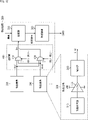
- FIG. 1 is a block diagram showing a configuration example of an imaging device 100.
- This imaging apparatus 100 includes an optical section 110 , an imaging element 200 , a recording section 120 and a control section 130 .
- As the imaging device 100 a camera mounted on an industrial robot, an in-vehicle camera, or the like is assumed.
- the optical unit 110 collects incident light and guides it to the imaging device 200 .
- the imaging element 200 photoelectrically converts incident light to capture image data.
- the image pickup device 200 performs predetermined signal processing such as image recognition processing on the captured image data, and outputs the processed data to the recording unit 120 via the signal line 209. .
- the recording unit 120 records data from the imaging device 200 .
- the control unit 130 controls the imaging device 200 to capture image data.
- FIG. 2 is a diagram showing an example of the layered structure of the imaging element 200.
- This imaging device 200 includes a detection chip 202 and a light receiving chip 201 stacked on the detection chip 202 . These chips are electrically connected through connections such as vias. In addition to vias, Cu--Cu bonding or bumps may be used for connection.
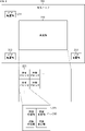
- FIG. 3 is an example of a plan view of the light receiving chip 201.
- the light receiving chip 201 is provided with a light receiving portion 220 , a via placement portion 211 , a via placement portion 212 , and a via placement portion 213 .
- Vias connected to the detection chip 202 are arranged in the via arrangement portions 211 , 212 and 213 .
- a plurality of shared blocks 221 are arranged in a two-dimensional lattice pattern in the light receiving section 220 .
- a plurality of logarithmic response units 310 are arranged in each of the shared blocks 221 .
- four logarithmic response units 310 are arranged in two rows by two columns. These four logarithmic responders 310 share circuitry on the detection chip 202 . The details of the shared circuit will be described later. Note that the number of logarithmic response units 310 in shared block 221 is not limited to four.
- the logarithmic response unit 310 generates a voltage signal corresponding to the logarithmic value of the photocurrent.
- Each logarithmic response unit 310 is assigned a pixel address consisting of a row address and a column address.
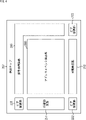
- FIG. 4 is an example of a plan view of the detection chip 202.
- the detection chip 202 is provided with a via placement section 231 , a via placement section 232 , a via placement section 233 , a signal processing circuit 240 , a row driving circuit 251 , a column driving circuit 252 and an address event detection section 260 .
- Vias connected to the light receiving chip 201 are arranged in the via arrangement portions 231 , 232 , and 233 .
- the address event detection section 260 detects the presence or absence of an address event for each logarithmic response section 310 and generates a detection signal indicating the detection result.
- the row drive circuit 251 selects a row address and causes the address event detector 260 to output a detection signal corresponding to the row address.
- the column drive circuit 252 selects a column address and causes the address event detection section 260 to output a detection signal corresponding to the column address.
- the signal processing circuit 240 performs predetermined signal processing on the detection signal from the address event detection section 260 .
- the signal processing circuit 240 arranges the detection signals as pixel signals in a two-dimensional lattice, and acquires image data having 2-bit information for each pixel. Then, the signal processing circuit 240 executes signal processing such as image recognition processing on the image data.
- FIG. 5 is an example of a plan view of the address event detector 260.
- FIG. A plurality of detection blocks 320 are arranged in the address event detection section 260 .
- a detection block 320 is arranged for each shared block 221 on the light receiving chip 201 .
- N is an integer
- N detection blocks 320 are arranged.
- Each detection block 320 is connected with a corresponding shared block 221 .
- FIG. 6 is a circuit diagram showing a configuration example of the logarithmic response section 310.
- the logarithmic response unit 310 includes a photoelectric conversion element 311 , nMOS (n-channel Metal Oxide Semiconductor) transistors 312 and 313 , and a pMOS (p-channel MOS) transistor 314 .
- the photoelectric conversion element 311 and the nMOS transistors 312 and 313 are arranged in the light receiving chip 201, and the pMOS transistor 314 is arranged in the detection chip 202, for example.
- the source of the nMOS transistor 312 is connected to the cathode of the photoelectric conversion element 311, and the drain is connected to the power supply terminal.
- the pMOS transistor 314 and the nMOS transistor 313 are connected in series between the power supply terminal and the ground terminal.
- a connection point between the pMOS transistor 314 and the nMOS transistor 313 is connected to the gate of the nMOS transistor 312 and the input terminal of the detection block 320 .
- a predetermined bias voltage Vbias1 is applied to the gate of the pMOS transistor 314 .
- nMOS transistors 312 and 313 are connected to the power supply side, and such a circuit is called a source follower. These two loop-connected source followers convert the photocurrent from the photoelectric conversion element 311 into a voltage signal corresponding to its logarithmic value.
- the pMOS transistor 314 supplies constant current to the nMOS transistor 313 .
- the ground of the light receiving chip 201 and the ground of the detection chip 202 are separated from each other for interference countermeasures.
- FIG. 7 is a block diagram showing a configuration example of the detection block 320.
- the detection block 320 includes multiple buffers 330 , multiple differentiators 340 , a selection section 400 , a comparison section 500 and a transfer circuit 360 .
- a buffer 330 and a differentiator 340 are arranged for each logarithmic response unit 310 in the shared block 221 . For example, if there are four logarithmic response units 310 in shared block 221, four buffers 330 and four differentiators 340 are arranged.
- the buffer 330 outputs the voltage signal from the corresponding logarithmic response section 310 to the differentiator 340 .
- This buffer 330 can improve the driving force for driving the subsequent stage.
- the buffer 330 can ensure noise isolation associated with subsequent switching operations.
- the differentiator 340 obtains the amount of change in the voltage signal as a differentiated signal.
- the differentiator 340 receives the voltage signal from the corresponding logarithmic response section 310 via the buffer 330 and obtains the amount of change in the voltage signal by differentiation.
- the differentiator 340 then supplies the differentiated signal to the selector 400 .
- the m-th differential signal Sin (m is an integer from 1 to M) in the detection block 320 is assumed to be Sinm.
- the selection unit 400 selects one of the M differentiated signals according to the selection signal from the row driving circuit 251 .
- This selection unit 400 comprises selectors 410 and 420 .
- M differentiated signals Sin are input to the selector 410 .
- the selector 410 selects one of these differentiated signals Sin according to the selection signal and supplies it to the comparator 500 as Sout+.
- the selector 420 also receives the M differentiated signals Sin.
- the selector 420 selects one of these differentiated signals Sin according to the selection signal and supplies it to the comparator 500 as Sout-.
- the comparison section 500 compares the differentiated signal (that is, the amount of change) selected by the selection section 400 with a predetermined threshold.
- the comparison unit 500 supplies a signal indicating the comparison result to the transfer circuit 360 as a detection signal.
- the transfer circuit 360 transfers the detection signal to the signal processing circuit 240 according to the column drive signal from the column drive circuit 252 .
- FIG. 8 is a circuit diagram showing a configuration example of the differentiator 340. As shown in FIG. This differentiator 340 comprises a capacitor 341 , a capacitor 343 , an inverter 342 and a switch 344 .
- Capacitor 343 is connected in parallel with inverter 342 .
- the switch 344 opens and closes the path connecting both ends of the capacitor 343 according to the row drive signal.
- the inverter 342 inverts the voltage signal input via the capacitor 341 .
- This inverter 342 outputs an inverted signal to the selection section 400 .
- Equation 5 Equation 5
- Equation 5 represents the subtraction operation of the voltage signal, and the gain of the subtraction result is C1/C2. Since it is usually desired to maximize the gain, it is preferable to design C1 large and C2 small. On the other hand, if C2 is too small, the kTC noise may increase and the noise characteristics may deteriorate, so the reduction of the capacitance of C2 is limited to the extent that the noise can be tolerated. In addition, since the differentiator 340 is mounted for each pixel, the capacitors C1 and C2 are restricted in area. With these considerations in mind, for example, C1 is set to a value between 20 and 200 femtofarads (fF) and C2 is set to a value between 1 and 20 femtofarads (fF).
- FIG. 9 is a circuit diagram showing a configuration example of the comparison section 500. As shown in FIG.
- the comparison unit 500 includes comparators 510 and 520 .
- the comparator 510 compares the differentiated signal Sout+ from the selector 410 with a predetermined upper limit threshold Vrefp.
- the comparator 510 supplies the comparison result to the transfer circuit 360 as the detection signal DET+.
- This detection signal DET+ indicates the presence or absence of an on-event.
- the on-event means that the amount of change in luminance exceeds a predetermined upper threshold.
- the comparator 520 compares the differentiated signal Sout- from the selector 420 with the lower threshold Vrefn lower than the upper threshold Vrefp.
- the comparator 520 supplies the comparison result to the transfer circuit 360 as the detection signal DET-.
- This detection signal DET- indicates the presence or absence of an OFF event.
- the off-event means that the amount of change in luminance has fallen below a predetermined lower threshold.
- the comparator 510 is an example of an upper limit side comparator
- the comparator 520 is an example of a lower limit side comparator.
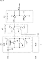
- FIG. 10 is a circuit diagram showing one configuration example of the differentiator 340, the selector 410, and the comparator 510.
- FIG. 10 is a circuit diagram showing one configuration example of the differentiator 340, the selector 410, and the comparator 510.
- the differentiator 340 includes a capacitor 341 , a capacitor 343 , a pMOS transistor 345 , a pMOS transistor 346 and an nMOS transistor 347 .
- the pMOS transistor 345 and the nMOS transistor 347 are connected in series between the power supply terminal and the ground terminal with the pMOS transistor 345 on the power supply side.
- a capacitor 341 is inserted between the gates of these pMOS transistor 345 and nMOS transistor 347 and the buffer 330 .
- a connection point between the pMOS transistor 345 and the nMOS transistor 347 is connected to the selector 410 . With this connection configuration, the pMOS transistor 345 and the nMOS transistor 347 function as an inverter 342 .
- a capacitor 343 and a pMOS transistor 346 are connected in parallel between the connection point of the pMOS transistor 345 and the nMOS transistor 347 and the capacitor 341 .
- This pMOS transistor 346 functions as a switch 344 .
- a plurality of pMOS transistors 411 are arranged in the selector 410 .
- a pMOS transistor 411 is arranged for each differentiator 340 .
- the pMOS transistor 411 is inserted between the corresponding differentiator 340 and comparator 510 .
- a selection signal SEL is individually input to each gate of the pMOS transistor 411 .
- the selection signal SEL of the m-th pMOS transistor 411 is assumed to be SELm. These selection signals SEL allow the row driving circuit 251 to turn on any one of the M pMOS transistors 411 and turn off the rest. Then, the differentiated signal Sout+ is output to the comparator 510 as a selected signal via the pMOS transistor 411 in the ON state. Note that the circuit configuration of the selector 420 is the same as that of the selector 410 .
- the comparator 510 includes a pMOS transistor 511 and an nMOS transistor 512 .
- the pMOS transistor 511 and the nMOS transistor 512 are connected in series between the power supply terminal and the ground terminal. Further, the differential signal Sout+ is input to the gate of the pMOS transistor 511 and the voltage of the upper limit threshold Vrefp is input to the gate of the nMOS transistor 512 .
- a connection point between the pMOS transistor 511 and the nMOS transistor 512 outputs a detection signal DET+. Note that the circuit configuration of the comparator 520 is the same as that of the comparator 510 .
- circuit configurations of the differentiator 340, the selector 410, and the comparator 510 are not limited to those illustrated in FIG. 10 as long as they have the functions described with reference to FIG.
- nMOS and pMOS transistors can be interchanged.
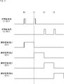
- FIG. 11 is a timing chart showing an example of control of the row driving circuit 251.
- the row drive circuit 251 selects the first row by the row drive signal L1 and drives the differentiator 340 of that row.
- This row driving signal L1 initializes the capacitor 343 in the differentiator 340 of the first row.
- the row driving circuit 251 selects the upper left portion of the 2 rows ⁇ 2 columns in the shared block 221 for a certain period of time according to the selection signal SEL1, and drives the selection section 400 . As a result, the presence or absence of an address event is detected in the odd-numbered columns of the first row.
- the row driving circuit 251 drives the differentiator 340 of the first row again with the row driving signal L1.
- the row driving circuit 251 selects the upper right portion of the 2 rows ⁇ 2 columns in the shared block 221 for a certain period of time according to the selection signal SEL2. As a result, the presence or absence of an address event is detected in the even columns of the first row.
- the row driving circuit 251 drives the differentiator 340 on the second row with the row driving signal L2.
- This row drive signal L2 initializes the capacitor 343 in the differentiator 340 on the second row.
- the row driving circuit 251 selects the lower left portion of the 2 rows ⁇ 2 columns in the shared block 221 for a certain period of time according to the selection signal SEL3. As a result, the presence or absence of an address event is detected in the odd-numbered columns of the second row.
- the row driving circuit 251 again drives the differentiator 340 in the second row with the row driving signal L2.
- the row driving circuit 251 selects the lower right portion of the 2 rows ⁇ 2 columns in the shared block 221 by the selection signal SEL4 for a certain period of time. As a result, the presence or absence of an address event is detected in the even-numbered columns of the second row.
- the row driving circuit 251 sequentially selects the rows in which the logarithmic response units 310 are arranged, and drives the selected rows with the row driving signal. Each time the row driving circuit 251 selects a row, it sequentially selects each of the detection pixels 300 in the shared block 221 of the selected row according to the selection signal. For example, if 2 rows by 2 columns of detection pixels 300 are arranged in shared block 221, each time a row is selected, the odd and even columns in that row are selected in turn.
- the row driving circuit 251 can also sequentially select the rows in which the shared blocks 221 are arranged, in other words, two rows of the logarithmic response units 310 . In this case, each time a row is selected, the four detection pixels within the shared block 221 of that row are selected in turn.
- FIG. 12 is a block diagram showing one configuration example of the detection pixel 300 and the detection circuit 305.
- the circuit comprising the selection unit 400, the comparison unit 500 and the transfer circuit 360 is referred to as a detection circuit 305.
- a plurality of detection pixels 300 share a detection circuit 305 .
- Each of the plurality of detection pixels 300 sharing the detection circuit 305 generates a voltage signal corresponding to the logarithmic value of the photocurrent. Then, each of the detection pixels 300 outputs a differential signal Sin indicating the amount of change in the voltage signal to the detection circuit 305 according to the row drive signal. In each of the detection pixels 300 , a voltage signal corresponding to the logarithmic value is generated by the logarithm responder 310 and a differentiated signal is generated by the differentiator 340 .
- Selection signals such as the selection signal SEL1 and the selection signal SEL2 are commonly input to the selectors 410 and 420 in the detection circuit 305 .
- the detection circuit 305 selects the differential signal of the detection pixel indicated by the selection signal, that is, the amount of change, among the plurality of detection pixels 300, and detects whether the amount of change exceeds a predetermined threshold.
- the detection circuit 305 then transfers the detection signal to the signal processing circuit 240 according to the column drive signal.
- the differential signal is selected by the selection section 400 and compared with the threshold value by the comparison section 500 . Also, the detection signal is transferred by the transfer circuit 360 .
- the comparison section 500 and the transfer circuit 360 are arranged for each detection pixel together with the logarithmic response section 310, the buffer 330 and the differentiator 340.
- the circuit scale of the image sensor 200 can be reduced compared to the case where the detection circuit 305 is not shared. can. This facilitates miniaturization of pixels.
- the circuit scale of the detection chip 202 is larger than that of the light receiving chip 201 . Therefore, the circuit on the detection chip 202 side limits the pixel density, making it difficult to miniaturize the pixels.
- the circuit scale of the detection chip 202 can be reduced and the pixels can be easily miniaturized.
- the buffer 330 is arranged for each detection pixel 300, the configuration is not limited to this, and a configuration without the buffer 330 is also possible.
- the photoelectric conversion element 311, the nMOS transistor 312, and the nMOS transistor 313 of the logarithmic response unit 310 are arranged on the light receiving chip 201, and the pMOS transistor 314 and subsequent ones are arranged on the detection chip 202, but the configuration is not limited to this.
- the photoelectric conversion element 311 can be arranged on the light receiving chip 201 and the rest can be arranged on the detection chip 202 .
- the logarithmic response unit 310 may be arranged on the light receiving chip 201 and arrange the buffer 330 and the rest on the detection chip 202 .
- the logarithmic response unit 310 and the buffer 330 may be arranged on the light receiving chip 201 and the differentiator 340 and subsequent elements may be arranged on the detection chip 202 .
- the logarithmic response unit 310, the buffer 330 and the differentiator 340 can be arranged on the light receiving chip 201, and the detection circuit 305 and subsequent circuits can be arranged on the detection chip 202.
- FIG. It is also possible to arrange up to the selection unit 400 in the light receiving chip 201 and arrange the comparison unit 500 and beyond in the detection chip 202 .
- FIG. 13 is a flowchart showing an example of the operation of the imaging device 200.
- This operation is started, for example, when a predetermined application for detecting the presence or absence of an address event is executed.
- the row driving circuit 251 selects any row (step S901). Then, the row driving circuit 251 selects and drives one of the detection pixels 300 in each shared block 221 in the selected row (step S902). The detection circuit 305 detects the presence or absence of an address event in the selected detection pixel 300 (step S903). After step S903, the imaging device 200 repeatedly executes step S901 and subsequent steps.
- the detection circuit 305 for detecting the presence or absence of an address event is shared by a plurality of detection pixels 300, the circuit scale can be reduced compared to the case where the detection circuit 305 is not shared. This facilitates miniaturization of the detection pixels 300 .
- the imaging device 200 has a structure in which the light receiving chip 201 and the detection chip 202 are stacked.
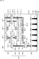
- FIG. 14 is a diagram showing a cross-sectional configuration example of the imaging element 200a in the first embodiment.
- the light receiving chip 201 is on the lower side in the figure, and the detection chip 202 is stacked on the upper side in the figure.
- the lower side in the figure is the incident surface side.
- the light-receiving chip 201 has an on-chip lens layer 601, a color filter layer 602, a photoelectric conversion element layer 603, and a wiring layer 604 stacked in order from the bottom in the figure.
- Photoelectric conversion elements 311 are formed in the photoelectric conversion element layer 603 , and inter-pixel separation portions 605 are formed between the photoelectric conversion elements 311 to prevent light from leaking into adjacent pixels.
- the wiring layer 604 gates such as the nMOS transistor 313 (FIG. 6) and a plurality of wirings (not shown) are formed.
- the detection chip 202 is formed as one semiconductor layer, and is a layer in which devices such as capacitive elements and transistors are formed on the front and back sides of one semiconductor substrate.
- the lower side of the detection chip 202 in the drawing is the rear surface, and the area on the rear surface side is the rear surface area 701a.
- the upper side in the drawing is defined as a surface, and the area on the surface side is described as a surface area 702a.
- Devices such as a plurality of transistors included in the detection chip 202 are formed in the back surface area 701a and the surface area 702a, respectively. That is, the detection chip 202 of the imaging device 200 shown in FIG. 14 has a configuration in which elements are provided on both sides of the semiconductor substrate. A separation layer 703a is provided between the back surface region 701a and the surface region 702a in order to separate the elements provided on both sides of the semiconductor substrate.
- the separation layer 703a may have any structure as long as it can electrically separate the back surface region 701a and the surface region 702a by an insulating film or an injection layer.
- the comparison section 500 and the transfer circuit 360 are arranged for each detection pixel together with the logarithmic response section 310, the buffer 330 and the differentiator 340. Therefore, the circuit scale of the detection chip 202 tends to be larger than that of the light receiving chip 201 . Therefore, the circuit on the detection chip 202 side limits the pixel density, making it difficult to miniaturize the pixels.
- the detector chip 202 having a large circuit scale can be made to have the same size as the light-receiving chip 201 and stacked without limiting the pixel density of the light-receiving chip 201. be able to.
- the circuit scale of the image sensor 200 can be reduced compared to the case where the detection circuit 305 is not shared. can be done. Therefore, when the detection circuit 305 is shared by a plurality of detection pixels 300, the size of the detection chip 202 can be further reduced, which facilitates miniaturization of the pixels.
- elements 711-1, 711-2, and 711-3 are formed in the back surface area 701a.
- Elements 721-1, 721-2, and 721-3 are formed in the surface region 702a.
- the elements 711-1 to 711-3 are simply referred to as the element 711 when there is no need to distinguish them individually. Other parts are similarly described.
- the element 711-1 is an element having a Pwell region
- the elements 711-2 and 711-3 are elements having an Nwell region
- Elements 721-1 to 721-3 are elements having Nwell regions.
- the example shown in FIG. 14 is an example and is not a description of limitation.
- the Pwell region included in the element 711-1 is connected to the wiring 742 through the gate 741.
- a contact 731 - 1 is connected to the wiring 742 . By connecting the contact 731-1 to the element 711-1, electrical control can be achieved.
- the other elements 711 and 721 also have gates and wirings similar to the element 711-1, and are configured to be electrically controllable by being connected to contacts.
- a contact 731-4 is connected to the element 711-2 and the element 711-3 formed in the back surface area 701a.
- a contact 731-2 is connected to the element 721-1 formed in the surface region 702a, and a contact 731-3 is connected to the element 721-2.
- the contact 731-5 is connected to a predetermined gate formed on the light receiving chip 201.
- the contacts 731-1 and 731-2 are connected to the electrode 751-1, and the contacts 731-3 to 731-5 are connected to the electrode 751-2.
- the electrodes 751-1 and 751-2 function as terminals connected to other chips (not shown).
- the elements 711 and 721 respectively formed in the back surface region 701a and the front surface region 702a are connected by the contacts 731.
- the light receiving chip 201 and the detection chip 202a are also connected by a contact 731.
- the element 711 and the surface area 702a formed in the back surface area 701a are switching elements such as transistors included in the detection chip 202, capacitive elements, resistive elements, and the like.
- Elements formed in the back surface region 701a and the front surface region 702a may be formed, for example, in one region by forming a device for which a good S value (subthreshold swing value) is desired, and in the other region. , to form a device that does not need to have a very good S value. That is, in this case, elements having different S-value characteristics can be arranged in the back surface region 701a and the surface region 702a.
- the elements formed earlier may be replaced with elements to be formed later.
- the elements formed in the back surface region 701a and the front surface region 702a are formed, for example, on one side to form an element driven at a low voltage and on the other side to form an element driven at a voltage higher than the low voltage. be able to. That is, in this case, elements with different driving voltages can be arranged in the back area 701a and the front area 702a.
- the elements formed in the back surface region 701a and the front surface region 702a for example, form an element with low noise in the vicinity of the gate on one side, and on the other side, the possibility of generating noise higher than the low noise.
- An element can be formed. That is, in this case, elements having different gate interface states can be arranged in the back surface region 701a and the surface region 702a.
- the imaging device 220a shown in FIG. 14 has three device layers formed of two semiconductor substrates.
- the elements included in the detection chip 202 can be accommodated more efficiently, and the imaging element 200 can be made more compact. .
- FIG. 15 is a diagram showing a cross-sectional configuration example of an imaging device 200b according to the second embodiment.
- An imaging device 200b shown in FIG. 15 differs from the imaging device 200a in the first embodiment in that a light receiving chip 201b and a detection chip 202b are directly bonded to each other via wiring layers.
- An imaging device 200b shown in FIG. 15 also has three device layers formed of two semiconductor substrates, like the imaging device 200a shown in FIG.
- Terminals (wirings) 611-1 to 611-3 for connecting to the detection chip 202b are provided on the surface side of the light receiving chip 201b.
- Terminals (wirings) 771-1 to 771-3 for connecting to the light receiving chip 201b are also provided on the back side of the detection chip 202b.
- Terminals 611-1, 611-2, and 611-3 of the light receiving chip 201b are connected to terminals 771-1, 771-2, and 771-3 of the detection chip 202b, respectively.
- the detection chip 202b of the imaging device 200b has elements formed on both sides of one semiconductor substrate, like the detection chip 202a of the imaging device 200a in the first embodiment.
- a back area 701b is formed on the back side of the detection chip 202b, and a surface area 702b is formed on the front side.
- An isolation layer 703b for electrically isolating the elements is formed between the back surface region 701b and the surface region 702b.
- the elements formed in the surface region 702a of the detection chip 202a shown in FIG. 14 are formed in the back surface region 701b of the detection chip 202b shown in FIG. That is, elements 721-1, 721-2, and 721-3 are formed in the back surface area 701b of the detection chip 202b shown in FIG.
- the elements formed in the back surface area 701a of the detection chip 202a shown in FIG. 14 are formed in the surface area 702b of the detection chip 202b shown in FIG. That is, elements 711-1, 711-2, and 711-3 are formed in the surface region 702b of the detection chip 202b shown in FIG.
- the elements formed in the back surface area 701 and the elements formed in the surface area 702 of the detection chip 202 may be elements included in the detection chip 202, and the elements formed are not limited.
- the element 721-1 of the detection chip 202b shown in FIG. 15 is connected to the terminal 771-1 via the contact 781-1.
- Element 721-2 is connected to terminal 771-2 via contact 781-2, and element 721-3 is connected to terminal 771-3 via contact 781-3.
- the element 711-1 of the detection chip 202b shown in FIG. 15 is connected to the terminal 791-1 via the contact 781-4.
- the elements 711-2 and 711-3 are connected to the terminal 791-2 via a shared wiring and contact 781-5.
- the detection chip 202b and the light receiving chip 201b are connected by directly joining the terminals provided on the surfaces of the respective chips. It is good as
- the elements included in the detection chip 202 can be accommodated more efficiently.
- the imaging element 200 can be made more compact.
- FIG. 16 is a diagram showing a cross-sectional configuration example of an imaging device 200c according to the third embodiment.
- the imaging device 200c shown in FIG. 16 is different from the imaging device 200a in the first and second embodiments in that the detection chip 202c stacked on the light receiving chip 201 is composed of two layers of the semiconductor layer 701c and the semiconductor layer 702c. , b.
- the semiconductor layer 701c corresponds to, for example, the back surface region 701a in the first embodiment, and the semiconductor layer 702c corresponds to the surface region 702a.
- Elements 811-1 to 811-3 configured to include Nwell regions are formed in the semiconductor layer 701c.
- Elements 821-1 to 821-3 each including a Pwell region are formed in the semiconductor layer 702c.
- the element 811-1 of the semiconductor layer 701c and the element 821-1 of the semiconductor layer 702c are connected via contacts 831-1, 831-2 and wiring 832-1.
- the elements 811-2 and 811-3 of the semiconductor layer 701c and the elements 821-2 and 821-3 of the semiconductor layer 702c are connected via contacts 831-3, 831-4 and wirings 832-2. .
- the contact 831-5 is connected to the gate of a predetermined transistor formed in the light receiving chip 201 and the wiring 832-3 formed in the detection chip 202c.
- the semiconductor layer 701c and the semiconductor layer 702c including such elements and contacts are bonded at the bonding surface, and the detection chip 202c and the light receiving chip 201 are bonded by bonding the semiconductor layer 701c and the semiconductor layer 702c.
- the imaging element 200c in the third embodiment is composed of three semiconductor substrates, and three device layers are formed.
- the detection chip 202c can also be formed with two semiconductor layers 701c and 702c.
- Elements formed in the semiconductor layer 701c and the semiconductor layer 702c can be elements having different characteristics. Elements with different characteristics are, for example, elements with heat resistance and other elements, elements with bad S-value characteristics and other elements, elements with low gate interface levels and low noise and other elements. element.
- FIG. 17 is a diagram showing a cross-sectional configuration example of an imaging device 200d according to the fourth embodiment.
- the imaging element 200d in the fourth embodiment is the same as in the first embodiment in that it includes a semiconductor substrate in which elements are formed on both sides of a single semiconductor substrate, as in the first embodiment. . Furthermore, the imaging element 200d in the fourth embodiment differs from the first embodiment in that another semiconductor substrate 901 is laminated on the detection chip 202d.
- the detection chip 202d of the imaging device 200d has elements formed on both sides of one semiconductor substrate.
- a back area 701d is formed on the back side of the detection chip 202d, and a surface area 702d is formed on the front side.
- An isolation layer 703d for electrically isolating the element is formed between the back surface region 701d and the surface region 702d.
- An element 851-1, an element 851-2, and an element 851-3 are formed in the back surface region 701d of the detection chip 202d shown in FIG.
- An element 861-1, an element 861-2, and an element 861-3 are formed on the surface region 702d of the detection chip 202d.
- the elements 851-1 and 851-2 of the detection chip 202d shown in FIG. 17 are connected to a terminal (wiring) 872-1 via a shared wiring and contact 871-1.
- An element 861-1 is also connected to a terminal (wiring) 872-1 via a contact 871-2.
- Element 851-3 is connected to terminal 872-2 via contact 871-4.
- An element 861-3 is also connected to the terminal 872-2 via a contact 871-3.
- a predetermined gate of the light receiving chip 201 is connected to a terminal (wiring) 872-3 via a contact 871-5.
- Terminals 872-1 to 872-3 are formed on the surface of the detection chip 202d.
- the terminals 872-1 through 872-3 are connected to terminals (wirings) 881-1 through 881-3 formed on the back surface of the semiconductor substrate 901, respectively.
- Elements 883 - 1 to 883 - 3 are formed on the semiconductor substrate 901 .
- Element 883-1 is connected to terminal 872-1 via contact 882-2.
- a contact 882-1 for connecting to a chip or the like outside the semiconductor substrate 901 is also connected to the terminal 872-1.
- Element 883-3 is connected to terminal 881-2 via contact 882-3.
- the light receiving chip 201 and the detection chip 202d of the imaging device 200d shown in FIG. 17 are connected via contacts.
- the detection chip 202d and the semiconductor substrate 901 are configured such that the substrates are directly bonded to each other.
- the imaging element 200d is configured such that three semiconductor substrates form four device layers.
- the elements included in the detection chip 202 can be accommodated more efficiently. , and the imaging device 200 can be made more compact.
- the semiconductor substrate 901 also has a configuration in which elements are formed on both sides of a single semiconductor substrate, in other words, a configuration in which two device layers are formed on a single semiconductor substrate. But it's okay.
- a configuration in which a plurality of semiconductor substrates in which two device layers are formed on one semiconductor substrate is stacked is also within the scope of application of this technology.
- FIG. 18 is a diagram showing a cross-sectional configuration example of an imaging device 200e according to the fifth embodiment.
- the image pickup device 200e in the fifth embodiment differs from the image pickup device 200d in the fourth embodiment in that the light receiving chip 201e and the detection chip 202e are directly joined, but the other points are the same. .
- a terminal (wiring) 912 is provided on the surface of the light receiving chip 201 e , and the terminal 912 is connected to a predetermined gate via a contact 911 .
- the terminal 912 is joined to a terminal (wiring) 913 formed on the back surface of the detection chip 202e.
- a contact 914 is connected to the terminal 913 .
- the light receiving chip 201e and the detection chip 202e of the imaging device 200e shown in FIG. 18 are configured such that the chips are directly joined together.
- the detection chip 202e and the semiconductor substrate 901 are configured such that the substrates are directly bonded to each other.
- the imaging device 200e is configured such that three semiconductor substrates form four device layers.
- the elements included in the detection chip 202 can be accommodated more efficiently. , and the imaging device 200 can be made more compact.
- the present technology can be applied to other than DVS.
- the present technology can also be applied to an imaging element used in an imaging device such as a camera that captures an image.
- the technology (the present technology) according to the present disclosure can be applied to various products.
- the technology according to the present disclosure is implemented as a device mounted on any type of moving object such as automobiles, electric vehicles, hybrid electric vehicles, motorcycles, bicycles, personal mobility, airplanes, drones, ships, and robots. may
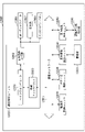
- FIG. 19 is a block diagram showing a schematic configuration example of a vehicle control system, which is an example of a mobile control system to which the technology according to the present disclosure can be applied.
- a vehicle control system 12000 includes a plurality of electronic control units connected via a communication network 12001.
- the vehicle control system 12000 includes a driving system control unit 12010, a body system control unit 12020, an outside information detection unit 12030, an inside information detection unit 12040, and an integrated control unit 12050.
- a microcomputer 12051, an audio/image output unit 12052, and an in-vehicle network I/F (Interface) 12053 are illustrated.
- the drive system control unit 12010 controls the operation of devices related to the drive system of the vehicle according to various programs.
- the driving system control unit 12010 includes a driving force generator for generating driving force of the vehicle such as an internal combustion engine or a driving motor, a driving force transmission mechanism for transmitting the driving force to the wheels, and a steering angle of the vehicle. It functions as a control device such as a steering mechanism to adjust and a brake device to generate braking force of the vehicle.
- the body system control unit 12020 controls the operation of various devices equipped on the vehicle body according to various programs.
- the body system control unit 12020 functions as a keyless entry system, a smart key system, a power window device, or a control device for various lamps such as headlamps, back lamps, brake lamps, winkers or fog lamps.
- the body system control unit 12020 can receive radio waves transmitted from a portable device that substitutes for a key or signals from various switches.
- the body system control unit 12020 receives the input of these radio waves or signals and controls the door lock device, power window device, lamps, etc. of the vehicle.
- the vehicle exterior information detection unit 12030 detects information outside the vehicle in which the vehicle control system 12000 is installed.
- the vehicle exterior information detection unit 12030 is connected with an imaging section 12031 .
- the vehicle exterior information detection unit 12030 causes the imaging unit 12031 to capture an image of the exterior of the vehicle, and receives the captured image.
- the vehicle exterior information detection unit 12030 may perform object detection processing or distance detection processing such as people, vehicles, obstacles, signs, or characters on the road surface based on the received image.
- the imaging unit 12031 is an optical sensor that receives light and outputs an electrical signal according to the amount of received light.
- the imaging unit 12031 can output the electric signal as an image, and can also output it as distance measurement information.
- the light received by the imaging unit 12031 may be visible light or non-visible light such as infrared rays.
- the in-vehicle information detection unit 12040 detects in-vehicle information.
- the in-vehicle information detection unit 12040 is connected to, for example, a driver state detection section 12041 that detects the state of the driver.
- the driver state detection unit 12041 includes, for example, a camera that captures an image of the driver, and the in-vehicle information detection unit 12040 detects the degree of fatigue or concentration of the driver based on the detection information input from the driver state detection unit 12041. It may be calculated, or it may be determined whether the driver is dozing off.
- the microcomputer 12051 calculates control target values for the driving force generator, the steering mechanism, or the braking device based on information on the inside and outside of the vehicle acquired by the vehicle exterior information detection unit 12030 or the vehicle interior information detection unit 12040, and controls the drive system control unit.
- a control command can be output to 12010 .
- the microcomputer 12051 realizes the functions of ADAS (Advanced Driver Assistance System) including collision avoidance or shock mitigation of vehicles, follow-up driving based on inter-vehicle distance, vehicle speed maintenance driving, vehicle collision warning, vehicle lane deviation warning, etc. Cooperative control can be performed for the purpose of ADAS (Advanced Driver Assistance System) including collision avoidance or shock mitigation of vehicles, follow-up driving based on inter-vehicle distance, vehicle speed maintenance driving, vehicle collision warning, vehicle lane deviation warning, etc. Cooperative control can be performed for the purpose of ADAS (Advanced Driver Assistance System) including collision avoidance or shock mitigation of vehicles, follow-up driving based on inter-vehicle distance, vehicle speed
- the microcomputer 12051 controls the driving force generator, the steering mechanism, the braking device, etc. based on the information about the vehicle surroundings acquired by the vehicle exterior information detection unit 12030 or the vehicle interior information detection unit 12040, so that the driver's Cooperative control can be performed for the purpose of autonomous driving, etc., in which vehicles autonomously travel without depending on operation.
- the microcomputer 12051 can output a control command to the body system control unit 12030 based on the information outside the vehicle acquired by the information detection unit 12030 outside the vehicle.
- the microcomputer 12051 controls the headlamps according to the position of the preceding vehicle or the oncoming vehicle detected by the vehicle exterior information detection unit 12030, and performs cooperative control aimed at anti-glare such as switching from high beam to low beam. It can be carried out.
- the audio/image output unit 12052 transmits at least one of audio and/or image output signals to an output device capable of visually or audibly notifying the passengers of the vehicle or the outside of the vehicle.
- an audio speaker 12061, a display unit 12062, and an instrument panel 12063 are illustrated as output devices.
- the display unit 12062 may include at least one of an on-board display and a head-up display, for example.
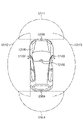
- FIG. 20 is a diagram showing an example of the installation position of the imaging unit 12031.
- FIG. 20 is a diagram showing an example of the installation position of the imaging unit 12031.
- the imaging unit 12031 has imaging units 12101, 12102, 12103, 12104, and 12105.
- the imaging units 12101, 12102, 12103, 12104, and 12105 are provided at positions such as the front nose, side mirrors, rear bumper, back door, and windshield of the vehicle 12100, for example.
- An image pickup unit 12101 provided in the front nose and an image pickup unit 12105 provided above the windshield in the passenger compartment mainly acquire images in front of the vehicle 12100 .
- Imaging units 12102 and 12103 provided in the side mirrors mainly acquire side images of the vehicle 12100 .
- An imaging unit 12104 provided in the rear bumper or back door mainly acquires an image behind the vehicle 12100 .
- the imaging unit 12105 provided above the windshield in the passenger compartment is mainly used for detecting preceding vehicles, pedestrians, obstacles, traffic lights, traffic signs, lanes, and the like.
- FIG. 20 shows an example of the imaging range of the imaging units 12101 to 12104.
- the imaging range 12111 indicates the imaging range of the imaging unit 12101 provided in the front nose
- the imaging ranges 12112 and 12113 indicate the imaging ranges of the imaging units 12102 and 12103 provided in the side mirrors, respectively
- the imaging range 12114 The imaging range of an imaging unit 12104 provided on the rear bumper or back door is shown. For example, by superimposing the image data captured by the imaging units 12101 to 12104, a bird's-eye view image of the vehicle 12100 viewed from above can be obtained.
- At least one of the imaging units 12101 to 12104 may have a function of acquiring distance information.
- at least one of the imaging units 12101 to 12104 may be a stereo camera composed of a plurality of imaging elements, or may be an imaging element having pixels for phase difference detection.
- the microcomputer 12051 determines the distance to each three-dimensional object within the imaging ranges 12111 to 12114 and changes in this distance over time (relative velocity with respect to the vehicle 12100). , it is possible to extract, as the preceding vehicle, the closest three-dimensional object on the traveling path of the vehicle 12100, which runs at a predetermined speed (for example, 0 km/h or more) in substantially the same direction as the vehicle 12100. can. Furthermore, the microcomputer 12051 can set the inter-vehicle distance to be secured in advance in front of the preceding vehicle, and perform automatic brake control (including following stop control) and automatic acceleration control (including following start control). In this way, cooperative control can be performed for the purpose of automatic driving in which the vehicle runs autonomously without relying on the operation of the driver.
- automatic brake control including following stop control
- automatic acceleration control including following start control
- the microcomputer 12051 converts three-dimensional object data related to three-dimensional objects to other three-dimensional objects such as motorcycles, ordinary vehicles, large vehicles, pedestrians, and utility poles. It can be classified and extracted and used for automatic avoidance of obstacles. For example, the microcomputer 12051 distinguishes obstacles around the vehicle 12100 into those that are visible to the driver of the vehicle 12100 and those that are difficult to see. Then, the microcomputer 12051 judges the collision risk indicating the degree of danger of collision with each obstacle, and when the collision risk is equal to or higher than the set value and there is a possibility of collision, an audio speaker 12061 and a display unit 12062 are displayed. By outputting an alarm to the driver via the drive system control unit 12010 and performing forced deceleration and avoidance steering via the drive system control unit 12010, driving support for collision avoidance can be performed.
- At least one of the imaging units 12101 to 12104 may be an infrared camera that detects infrared rays.
- the microcomputer 12051 can recognize a pedestrian by determining whether or not the pedestrian exists in the captured images of the imaging units 12101 to 12104 .
- recognition of a pedestrian is performed by, for example, a procedure for extracting feature points in images captured by the imaging units 12101 to 12104 as infrared cameras, and performing pattern matching processing on a series of feature points indicating the outline of an object to determine whether or not the pedestrian is a pedestrian.
- the audio image output unit 12052 outputs a rectangular outline for emphasis to the recognized pedestrian. is superimposed on the display unit 12062 . Also, the audio/image output unit 12052 may control the display unit 12062 to display an icon or the like indicating a pedestrian at a desired position.
- the system represents an entire device composed of multiple devices.
- the present technology can also take the following configuration.
- a first substrate including a plurality of sensing pixels that generate voltage signals responsive to the logarithm of the photocurrent; a second substrate including a detection circuit for detecting whether or not the amount of change in the voltage signal of the detection pixel indicated by the input selection signal exceeds a predetermined threshold among the plurality of detection pixels;
- An imaging device wherein elements constituting the detection circuit are arranged in each of a first region on the back surface side and a second region on the front surface side of the second substrate.
- the imaging device according to (1) further comprising a separation layer between the first region and the second region that electrically separates the first region and the second region.
- a plurality of sensing pixels each generating a voltage signal responsive to the logarithm of the photocurrent; a detection circuit for detecting whether or not a variation in the voltage signal of one of the plurality of detection pixels indicated by the input selection signal exceeds a predetermined threshold; a signal processing unit that processes a detection signal indicating the detection result of the detection circuit,
- An imaging device wherein elements constituting the detection circuit are arranged respectively in a region on the back side and a region on the front side of a substrate including the detection circuit.
Landscapes
- Engineering & Computer Science (AREA)
- Multimedia (AREA)
- Signal Processing (AREA)
- Solid State Image Pick-Up Elements (AREA)
- Transforming Light Signals Into Electric Signals (AREA)
Abstract
Description
図1は、撮像装置100の構成例を示すブロック図である。この撮像装置100は、光学部110、撮像素子200、記録部120および制御部130を備える。撮像装置100としては、産業用ロボットに搭載されるカメラや、車載カメラなどが想定される。
図2は、撮像素子200の積層構造の一例を示す図である。この撮像素子200は、検出チップ202と、その検出チップ202に積層された受光チップ201とを備える。これらのチップは、ビアなどの接続部を介して電気的に接続される。なお、ビアの他、Cu-Cu接合やバンプにより接続することもできる。
図6は、対数応答部310の一構成例を示す回路図である。この対数応答部310は、光電変換素子311、nMOS(n-channel Metal Oxide Semiconductor)トランジスタ312,313、pMOS(p-channel MOS)トランジスタ314を備える。これらのうち光電変換素子311、nMOSトランジスタ312,313は、例えば、受光チップ201に配置され、pMOSトランジスタ314は、検出チップ202に配置される。
図7は、検出ブロック320の一構成例を示すブロック図である。検出ブロック320は、複数のバッファ330、複数の微分器340、選択部400、比較部500、転送回路360を備える。バッファ330と微分器340は、共有ブロック221内の対数応答部310ごとに配置される。例えば、共有ブロック221内の対数応答部310が4つである場合、バッファ330および微分器340は、4つずつ配置される。
図8は、微分器340の一構成例を示す回路図である。この微分器340は、コンデンサ341、コンデンサ343、インバータ342、スイッチ344を備える。
Qinit=C1×Vinit ・・・式1
Qafter=C1×Vafter ・・・式2
Q2=-C2×Vout ・・・式3
Qinit=Qafter+Q2 ・・・式4
Vout=-(C1/C2)×(Vafter-Vinit) ・・・式5
図9は、比較部500の一構成例を示す回路図である。この比較部500は、コンパレータ510、コンパレータ520を備える。
図13は、撮像素子200の動作の一例を示すフローチャートである。この動作は、例えば、アドレスイベントの有無を検出するための所定のアプリケーションが実行されたときに開始される。
図2を参照して説明したように、撮像素子200は、受光チップ201と検出チップ202が積層された構成とされている。図14は、第1の実施の形態における撮像素子200aの断面構成例を示す図である。
図15は、第2の実施の形態における撮像素子200bの断面構成例を示す図である。
図16は、第3の実施の形態における撮像素子200cの断面構成例を示す図である。
図17は、第4の実施の形態における撮像素子200dの断面構成例を示す図である。
図18は、第5の実施の形態における撮像素子200eの断面構成例を示す図である。
本開示に係る技術(本技術)は、様々な製品へ応用することができる。例えば、本開示に係る技術は、自動車、電気自動車、ハイブリッド電気自動車、自動二輪車、自転車、パーソナルモビリティ、飛行機、ドローン、船舶、ロボット等のいずれかの種類の移動体に搭載される装置として実現されてもよい。
(1)
光電流の対数値に応じた電圧信号を生成する複数の検出画素を含む第1の基板と、
前記複数の検出画素のうち、入力された選択信号の示す検出画素の前記電圧信号の変化量が所定の閾値を超えたか否かを検出する検出回路を含む第2の基板と
が積層され、
前記第2の基板の裏面側の第1の領域と表面側の第2の領域のそれぞれに前記検出回路を構成する素子が配置されている
撮像素子。
(2)
前記第1の領域と前記第2の領域との間に、前記第1の領域と前記第2の領域を電気的に分離する分離層をさらに備える
前記(1)に記載の撮像素子。
(3)
前記第1の領域に配置されている素子と前記第2の領域に配置されている素子は、S値特性が異なる
前記(1)または(2)に記載の撮像素子。
(4)
前記第1の領域に配置されている素子と前記第2の領域に配置されている素子は、熱耐性が異なる
前記(1)乃至(3)のいずれかに記載の撮像素子。
(5)
前記第1の領域に配置されている素子と前記第2の領域に配置されている素子は、駆動電圧が異なる
前記(1)乃至(4)のいずれかに記載の撮像素子。
(6)
前記第1の領域に配置されている素子と前記第2の領域に配置されている素子は、ゲートの界面順位が異なる
前記(1)乃至(5)のいずれかに記載の撮像素子。
(7)
前記第1の基板内の素子と前記第2の基板内の素子はコンタクトにより接続されている
前記(1)乃至(6)のいずれかに記載の撮像素子。
(8)
前記第1の基板に設けられている配線と前記第2の基板に設けられている配線が接合されている
前記(1)乃至(6)のいずれかに記載の撮像素子。
(9)
前記第2の基板に第3の基板がさらに積層されている
前記(1)乃至(8)のいずれかに記載の撮像素子。
(10)
前記第2の基板に設けられている配線と前記第3の基板に設けられている配線が接合されている
前記(9)に記載の撮像素子。
(11)
光電流の対数値に応じた電圧信号を各々が生成する複数の検出画素と、
前記複数の検出画素のうち、入力された選択信号の示す検出画素の前記電圧信号の変化量が所定の閾値を超えたか否かを検出する検出回路と、
前記検出回路の検出結果を示す検出信号を処理する信号処理部と
を備え、
前記検出回路を含む基板の裏面側の領域と表面側の領域のそれぞれに前記検出回路を構成する素子が配置されている
撮像装置。
Claims (11)
- 光電流の対数値に応じた電圧信号を生成する複数の検出画素を含む第1の基板と、
前記複数の検出画素のうち、入力された選択信号の示す検出画素の前記電圧信号の変化量が所定の閾値を超えたか否かを検出する検出回路を含む第2の基板と
が積層され、
前記第2の基板の裏面側の第1の領域と表面側の第2の領域のそれぞれに前記検出回路を構成する素子が配置されている
撮像素子。 - 前記第1の領域と前記第2の領域との間に、前記第1の領域と前記第2の領域を電気的に分離する分離層をさらに備える
請求項1に記載の撮像素子。 - 前記第1の領域に配置されている素子と前記第2の領域に配置されている素子は、S値特性が異なる
請求項1に記載の撮像素子。 - 前記第1の領域に配置されている素子と前記第2の領域に配置されている素子は、熱耐性が異なる
請求項1に記載の撮像素子。 - 前記第1の領域に配置されている素子と前記第2の領域に配置されている素子は、駆動電圧が異なる
請求項1に記載の撮像素子。 - 前記第1の領域に配置されている素子と前記第2の領域に配置されている素子は、ゲートの界面順位が異なる
請求項1に記載の撮像素子。 - 前記第1の基板内の素子と前記第2の基板内の素子はコンタクトにより接続されている
請求項1に記載の撮像素子。 - 前記第1の基板に設けられている配線と前記第2の基板に設けられている配線が接合されている
請求項1に記載の撮像素子。 - 前記第2の基板に第3の基板がさらに積層されている
請求項1に記載の撮像素子。 - 前記第2の基板に設けられている配線と前記第3の基板に設けられている配線が接合されている
請求項9に記載の撮像素子。 - 光電流の対数値に応じた電圧信号を各々が生成する複数の検出画素と、
前記複数の検出画素のうち、入力された選択信号の示す検出画素の前記電圧信号の変化量が所定の閾値を超えたか否かを検出する検出回路と、
前記検出回路の検出結果を示す検出信号を処理する信号処理部と
を備え、
前記検出回路を含む基板の裏面側の領域と表面側の領域のそれぞれに前記検出回路を構成する素子が配置されている
撮像装置。
Priority Applications (2)
| Application Number | Priority Date | Filing Date | Title |
|---|---|---|---|
| CN202180089457.2A CN116745916A (zh) | 2021-01-22 | 2021-12-28 | 摄像元件和摄像装置 |
| US18/261,364 US12563317B2 (en) | 2021-01-22 | 2021-12-28 | Imaging element and imaging device |
Applications Claiming Priority (2)
| Application Number | Priority Date | Filing Date | Title |
|---|---|---|---|
| JP2021-008506 | 2021-01-22 | ||
| JP2021008506A JP2022112642A (ja) | 2021-01-22 | 2021-01-22 | 撮像素子、撮像装置 |
Publications (1)
| Publication Number | Publication Date |
|---|---|
| WO2022158278A1 true WO2022158278A1 (ja) | 2022-07-28 |
Family
ID=82548791
Family Applications (1)
| Application Number | Title | Priority Date | Filing Date |
|---|---|---|---|
| PCT/JP2021/048958 Ceased WO2022158278A1 (ja) | 2021-01-22 | 2021-12-28 | 撮像素子、撮像装置 |
Country Status (4)
| Country | Link |
|---|---|
| US (1) | US12563317B2 (ja) |
| JP (1) | JP2022112642A (ja) |
| CN (1) | CN116745916A (ja) |
| WO (1) | WO2022158278A1 (ja) |
Families Citing this family (3)
| Publication number | Priority date | Publication date | Assignee | Title |
|---|---|---|---|---|
| TW202446087A (zh) * | 2023-03-29 | 2024-11-16 | 日商索尼半導體解決方案公司 | 光檢測裝置及電子機器 |
| WO2024247511A1 (ja) * | 2023-05-26 | 2024-12-05 | ソニーセミコンダクタソリューションズ株式会社 | 固体撮像素子 |
| WO2025229794A1 (ja) * | 2024-05-01 | 2025-11-06 | ソニーセミコンダクタソリューションズ株式会社 | イメージセンサ |
Citations (2)
| Publication number | Priority date | Publication date | Assignee | Title |
|---|---|---|---|---|
| JP2019195135A (ja) * | 2018-05-02 | 2019-11-07 | ソニーセミコンダクタソリューションズ株式会社 | 固体撮像素子および撮像装置 |
| JP2020161993A (ja) * | 2019-03-27 | 2020-10-01 | ソニー株式会社 | 撮像システム及び物体認識システム |
Family Cites Families (4)
| Publication number | Priority date | Publication date | Assignee | Title |
|---|---|---|---|---|
| JP5244587B2 (ja) | 2005-06-03 | 2013-07-24 | ウニヴェルズィテート チューリッヒ | 時間依存性の画像データを検出するフォトアレイ |
| JP7029890B2 (ja) * | 2017-03-02 | 2022-03-04 | ソニーセミコンダクタソリューションズ株式会社 | 撮像素子、撮像素子の制御方法、及び、電子機器 |
| TWI897055B (zh) * | 2018-01-23 | 2025-09-11 | 日商索尼半導體解決方案公司 | 光檢測裝置及車輛控制系統 |
| US11574942B2 (en) * | 2018-12-12 | 2023-02-07 | Artilux, Inc. | Semiconductor device with low dark noise |
-
2021
- 2021-01-22 JP JP2021008506A patent/JP2022112642A/ja active Pending
- 2021-12-28 WO PCT/JP2021/048958 patent/WO2022158278A1/ja not_active Ceased
- 2021-12-28 CN CN202180089457.2A patent/CN116745916A/zh active Pending
- 2021-12-28 US US18/261,364 patent/US12563317B2/en active Active
Patent Citations (2)
| Publication number | Priority date | Publication date | Assignee | Title |
|---|---|---|---|---|
| JP2019195135A (ja) * | 2018-05-02 | 2019-11-07 | ソニーセミコンダクタソリューションズ株式会社 | 固体撮像素子および撮像装置 |
| JP2020161993A (ja) * | 2019-03-27 | 2020-10-01 | ソニー株式会社 | 撮像システム及び物体認識システム |
Also Published As
| Publication number | Publication date |
|---|---|
| US12563317B2 (en) | 2026-02-24 |
| CN116745916A (zh) | 2023-09-12 |
| US20240064433A1 (en) | 2024-02-22 |
| JP2022112642A (ja) | 2022-08-03 |
Similar Documents
| Publication | Publication Date | Title |
|---|---|---|
| US20230043681A1 (en) | Solid-state imaging device | |
| CN111656770B (zh) | 固态成像元件、成像装置及固态成像元件的控制方法 | |
| JP7611147B2 (ja) | 固体撮像素子、撮像装置、および、固体撮像素子の制御方法 | |
| JP7148269B2 (ja) | 固体撮像素子および撮像装置 | |
| US11076148B2 (en) | Solid-state image sensor, imaging apparatus, and method for controlling solid-state image sensor | |
| US20240236519A1 (en) | Imaging device, electronic device, and light detecting method | |
| JP7645260B2 (ja) | 固体撮像装置及び撮像装置 | |
| US12563317B2 (en) | Imaging element and imaging device | |
| WO2022064867A1 (ja) | 固体撮像素子、および、撮像装置 | |
| WO2019187685A1 (ja) | 固体撮像素子、撮像装置、および、固体撮像素子の制御方法 | |
| JP2019176334A (ja) | 固体撮像素子、テストシステム、および、固体撮像素子の制御方法 | |
| CN114830629A (zh) | 固态成像元件和成像装置 | |
| WO2020071103A1 (ja) | 半導体装置およびその製造方法、撮像素子 | |
| CN119769202A (zh) | 光检测元件和电子设备 | |
| WO2024043068A1 (ja) | 固体撮像素子および電子機器 | |
| WO2023026524A1 (ja) | 光検出デバイスおよび光検出装置 | |
| JP2020017552A (ja) | 固体撮像素子、撮像装置、および、固体撮像素子の制御方法 | |
| JP2026064327A (ja) | 電圧電流変換回路および撮像装置 | |
| WO2025110015A1 (ja) | 光検出装置及び電子機器 | |
| WO2023032284A1 (ja) | 固体撮像装置 | |
| WO2023013178A1 (ja) | 固体撮像装置及び電子機器 | |
| CN117413529A (zh) | 图像捕获装置及电子设备 |
Legal Events
| Date | Code | Title | Description |
|---|---|---|---|
| 121 | Ep: the epo has been informed by wipo that ep was designated in this application |
Ref document number: 21921379 Country of ref document: EP Kind code of ref document: A1 |
|
| WWE | Wipo information: entry into national phase |
Ref document number: 202180089457.2 Country of ref document: CN |
|
| WWE | Wipo information: entry into national phase |
Ref document number: 18261364 Country of ref document: US |
|
| NENP | Non-entry into the national phase |
Ref country code: DE |
|
| 122 | Ep: pct application non-entry in european phase |
Ref document number: 21921379 Country of ref document: EP Kind code of ref document: A1 |
|
| WWG | Wipo information: grant in national office |
Ref document number: 18261364 Country of ref document: US |