WO2022153139A1 - 表示装置の作製方法、表示装置、表示モジュール、及び、電子機器 - Google Patents
表示装置の作製方法、表示装置、表示モジュール、及び、電子機器 Download PDFInfo
- Publication number
- WO2022153139A1 WO2022153139A1 PCT/IB2022/050052 IB2022050052W WO2022153139A1 WO 2022153139 A1 WO2022153139 A1 WO 2022153139A1 IB 2022050052 W IB2022050052 W IB 2022050052W WO 2022153139 A1 WO2022153139 A1 WO 2022153139A1
- Authority
- WO
- WIPO (PCT)
- Prior art keywords
- layer
- light emitting
- transport layer
- electron transport
- electron
- Prior art date
Links
- 238000004519 manufacturing process Methods 0.000 title claims description 56
- 238000002347 injection Methods 0.000 claims abstract description 172
- 239000007924 injection Substances 0.000 claims abstract description 172
- 230000005525 hole transport Effects 0.000 claims abstract description 110
- 239000003086 colorant Substances 0.000 claims abstract description 20
- 239000010410 layer Substances 0.000 claims description 1166
- 238000000034 method Methods 0.000 claims description 167
- 239000011241 protective layer Substances 0.000 claims description 40
- 238000012545 processing Methods 0.000 claims description 23
- 239000011810 insulating material Substances 0.000 claims description 16
- 230000008569 process Effects 0.000 claims description 16
- 239000012212 insulator Substances 0.000 claims description 7
- 230000006870 function Effects 0.000 abstract description 86
- 239000010408 film Substances 0.000 description 185
- 230000032258 transport Effects 0.000 description 145
- 239000004065 semiconductor Substances 0.000 description 107
- 239000000463 material Substances 0.000 description 76
- 239000000758 substrate Substances 0.000 description 64
- 239000011701 zinc Substances 0.000 description 47
- 239000013078 crystal Substances 0.000 description 42
- 239000000126 substance Substances 0.000 description 38
- 229920005989 resin Polymers 0.000 description 29
- 239000011347 resin Substances 0.000 description 29
- 229910052751 metal Inorganic materials 0.000 description 28
- IJGRMHOSHXDMSA-UHFFFAOYSA-N Atomic nitrogen Chemical compound N#N IJGRMHOSHXDMSA-UHFFFAOYSA-N 0.000 description 25
- 239000002184 metal Substances 0.000 description 24
- 239000007789 gas Substances 0.000 description 21
- 239000000203 mixture Substances 0.000 description 21
- 238000007740 vapor deposition Methods 0.000 description 20
- PXHVJJICTQNCMI-UHFFFAOYSA-N Nickel Chemical compound [Ni] PXHVJJICTQNCMI-UHFFFAOYSA-N 0.000 description 19
- 238000004891 communication Methods 0.000 description 19
- 229910052760 oxygen Inorganic materials 0.000 description 19
- QVGXLLKOCUKJST-UHFFFAOYSA-N atomic oxygen Chemical compound [O] QVGXLLKOCUKJST-UHFFFAOYSA-N 0.000 description 17
- 239000012535 impurity Substances 0.000 description 17
- 230000003287 optical effect Effects 0.000 description 17
- 239000001301 oxygen Substances 0.000 description 17
- 125000004429 atom Chemical group 0.000 description 16
- 238000009413 insulation Methods 0.000 description 16
- 229910044991 metal oxide Inorganic materials 0.000 description 16
- 150000004706 metal oxides Chemical class 0.000 description 16
- 238000005530 etching Methods 0.000 description 15
- 239000001257 hydrogen Substances 0.000 description 15
- 229910052739 hydrogen Inorganic materials 0.000 description 15
- 150000004767 nitrides Chemical class 0.000 description 15
- XEEYBQQBJWHFJM-UHFFFAOYSA-N Iron Chemical compound [Fe] XEEYBQQBJWHFJM-UHFFFAOYSA-N 0.000 description 13
- UFHFLCQGNIYNRP-UHFFFAOYSA-N Hydrogen Chemical compound [H][H] UFHFLCQGNIYNRP-UHFFFAOYSA-N 0.000 description 12
- 238000005229 chemical vapour deposition Methods 0.000 description 12
- 229910052733 gallium Inorganic materials 0.000 description 12
- 229910052738 indium Inorganic materials 0.000 description 12
- 229910052757 nitrogen Inorganic materials 0.000 description 12
- 238000004544 sputter deposition Methods 0.000 description 12
- 239000010936 titanium Substances 0.000 description 12
- VYPSYNLAJGMNEJ-UHFFFAOYSA-N Silicium dioxide Chemical compound O=[Si]=O VYPSYNLAJGMNEJ-UHFFFAOYSA-N 0.000 description 11
- XUIMIQQOPSSXEZ-UHFFFAOYSA-N Silicon Chemical compound [Si] XUIMIQQOPSSXEZ-UHFFFAOYSA-N 0.000 description 11
- -1 Zn oxide Chemical compound 0.000 description 11
- 239000000956 alloy Substances 0.000 description 11
- 229910052782 aluminium Inorganic materials 0.000 description 11
- XAGFODPZIPBFFR-UHFFFAOYSA-N aluminium Chemical compound [Al] XAGFODPZIPBFFR-UHFFFAOYSA-N 0.000 description 11
- 238000000231 atomic layer deposition Methods 0.000 description 11
- 230000015572 biosynthetic process Effects 0.000 description 11
- 230000006378 damage Effects 0.000 description 11
- TWNQGVIAIRXVLR-UHFFFAOYSA-N oxo(oxoalumanyloxy)alumane Chemical compound O=[Al]O[Al]=O TWNQGVIAIRXVLR-UHFFFAOYSA-N 0.000 description 11
- 229910052710 silicon Inorganic materials 0.000 description 11
- 239000010703 silicon Substances 0.000 description 11
- 239000010409 thin film Substances 0.000 description 11
- GYHNNYVSQQEPJS-UHFFFAOYSA-N Gallium Chemical compound [Ga] GYHNNYVSQQEPJS-UHFFFAOYSA-N 0.000 description 10
- RTAQQCXQSZGOHL-UHFFFAOYSA-N Titanium Chemical compound [Ti] RTAQQCXQSZGOHL-UHFFFAOYSA-N 0.000 description 10
- APFVFJFRJDLVQX-UHFFFAOYSA-N indium atom Chemical compound [In] APFVFJFRJDLVQX-UHFFFAOYSA-N 0.000 description 10
- 229910052719 titanium Inorganic materials 0.000 description 10
- XLYOFNOQVPJJNP-UHFFFAOYSA-N water Substances O XLYOFNOQVPJJNP-UHFFFAOYSA-N 0.000 description 10
- 229910052581 Si3N4 Inorganic materials 0.000 description 9
- XLOMVQKBTHCTTD-UHFFFAOYSA-N Zinc monoxide Chemical compound [Zn]=O XLOMVQKBTHCTTD-UHFFFAOYSA-N 0.000 description 9
- 238000001312 dry etching Methods 0.000 description 9
- 229910052759 nickel Inorganic materials 0.000 description 9
- BASFCYQUMIYNBI-UHFFFAOYSA-N platinum Chemical compound [Pt] BASFCYQUMIYNBI-UHFFFAOYSA-N 0.000 description 9
- HQVNEWCFYHHQES-UHFFFAOYSA-N silicon nitride Chemical compound N12[Si]34N5[Si]62N3[Si]51N64 HQVNEWCFYHHQES-UHFFFAOYSA-N 0.000 description 9
- 239000000853 adhesive Substances 0.000 description 8
- 230000001070 adhesive effect Effects 0.000 description 8
- 229910045601 alloy Inorganic materials 0.000 description 8
- 150000001875 compounds Chemical class 0.000 description 8
- 238000007639 printing Methods 0.000 description 8
- 238000001039 wet etching Methods 0.000 description 8
- ZOKXTWBITQBERF-UHFFFAOYSA-N Molybdenum Chemical compound [Mo] ZOKXTWBITQBERF-UHFFFAOYSA-N 0.000 description 7
- KDLHZDBZIXYQEI-UHFFFAOYSA-N Palladium Chemical compound [Pd] KDLHZDBZIXYQEI-UHFFFAOYSA-N 0.000 description 7
- 238000000576 coating method Methods 0.000 description 7
- 239000010949 copper Substances 0.000 description 7
- 230000007547 defect Effects 0.000 description 7
- 238000010894 electron beam technology Methods 0.000 description 7
- 230000007246 mechanism Effects 0.000 description 7
- 229910052750 molybdenum Inorganic materials 0.000 description 7
- 239000011733 molybdenum Substances 0.000 description 7
- 229910052814 silicon oxide Inorganic materials 0.000 description 7
- 238000012546 transfer Methods 0.000 description 7
- WFKWXMTUELFFGS-UHFFFAOYSA-N tungsten Chemical compound [W] WFKWXMTUELFFGS-UHFFFAOYSA-N 0.000 description 7
- 229910052721 tungsten Inorganic materials 0.000 description 7
- 239000010937 tungsten Substances 0.000 description 7
- 239000011800 void material Substances 0.000 description 7
- 229910052727 yttrium Inorganic materials 0.000 description 7
- XKRFYHLGVUSROY-UHFFFAOYSA-N Argon Chemical compound [Ar] XKRFYHLGVUSROY-UHFFFAOYSA-N 0.000 description 6
- RYGMFSIKBFXOCR-UHFFFAOYSA-N Copper Chemical compound [Cu] RYGMFSIKBFXOCR-UHFFFAOYSA-N 0.000 description 6
- FYYHWMGAXLPEAU-UHFFFAOYSA-N Magnesium Chemical compound [Mg] FYYHWMGAXLPEAU-UHFFFAOYSA-N 0.000 description 6
- 229910052783 alkali metal Inorganic materials 0.000 description 6
- 150000001340 alkali metals Chemical class 0.000 description 6
- 229910052784 alkaline earth metal Inorganic materials 0.000 description 6
- 150000001342 alkaline earth metals Chemical class 0.000 description 6
- 150000004696 coordination complex Chemical class 0.000 description 6
- 229910052802 copper Inorganic materials 0.000 description 6
- 238000010586 diagram Methods 0.000 description 6
- 239000011521 glass Substances 0.000 description 6
- 238000003384 imaging method Methods 0.000 description 6
- 229910052742 iron Inorganic materials 0.000 description 6
- 239000011777 magnesium Substances 0.000 description 6
- 239000007769 metal material Substances 0.000 description 6
- 150000002894 organic compounds Chemical class 0.000 description 6
- 238000001228 spectrum Methods 0.000 description 6
- VWQVUPCCIRVNHF-UHFFFAOYSA-N yttrium atom Chemical compound [Y] VWQVUPCCIRVNHF-UHFFFAOYSA-N 0.000 description 6
- OKTJSMMVPCPJKN-UHFFFAOYSA-N Carbon Chemical compound [C] OKTJSMMVPCPJKN-UHFFFAOYSA-N 0.000 description 5
- ATJFFYVFTNAWJD-UHFFFAOYSA-N Tin Chemical compound [Sn] ATJFFYVFTNAWJD-UHFFFAOYSA-N 0.000 description 5
- QCWXUUIWCKQGHC-UHFFFAOYSA-N Zirconium Chemical compound [Zr] QCWXUUIWCKQGHC-UHFFFAOYSA-N 0.000 description 5
- 238000010521 absorption reaction Methods 0.000 description 5
- 229910052796 boron Inorganic materials 0.000 description 5
- 239000000969 carrier Substances 0.000 description 5
- 239000011651 chromium Substances 0.000 description 5
- 238000002003 electron diffraction Methods 0.000 description 5
- 229910052749 magnesium Inorganic materials 0.000 description 5
- 239000002159 nanocrystal Substances 0.000 description 5
- 229910052718 tin Inorganic materials 0.000 description 5
- 229910052725 zinc Inorganic materials 0.000 description 5
- 239000011787 zinc oxide Substances 0.000 description 5
- 229910052726 zirconium Inorganic materials 0.000 description 5
- 229920000178 Acrylic resin Polymers 0.000 description 4
- 239000004925 Acrylic resin Substances 0.000 description 4
- VYZAMTAEIAYCRO-UHFFFAOYSA-N Chromium Chemical compound [Cr] VYZAMTAEIAYCRO-UHFFFAOYSA-N 0.000 description 4
- 229910001111 Fine metal Inorganic materials 0.000 description 4
- 229910052779 Neodymium Inorganic materials 0.000 description 4
- NBIIXXVUZAFLBC-UHFFFAOYSA-N Phosphoric acid Chemical compound OP(O)(O)=O NBIIXXVUZAFLBC-UHFFFAOYSA-N 0.000 description 4
- BQCADISMDOOEFD-UHFFFAOYSA-N Silver Chemical compound [Ag] BQCADISMDOOEFD-UHFFFAOYSA-N 0.000 description 4
- XJHCXCQVJFPJIK-UHFFFAOYSA-M caesium fluoride Chemical compound [F-].[Cs+] XJHCXCQVJFPJIK-UHFFFAOYSA-M 0.000 description 4
- 238000006243 chemical reaction Methods 0.000 description 4
- 229910052804 chromium Inorganic materials 0.000 description 4
- 239000010941 cobalt Substances 0.000 description 4
- 229910017052 cobalt Inorganic materials 0.000 description 4
- GUTLYIVDDKVIGB-UHFFFAOYSA-N cobalt atom Chemical compound [Co] GUTLYIVDDKVIGB-UHFFFAOYSA-N 0.000 description 4
- 238000001514 detection method Methods 0.000 description 4
- 230000006866 deterioration Effects 0.000 description 4
- 230000000694 effects Effects 0.000 description 4
- 238000002149 energy-dispersive X-ray emission spectroscopy Methods 0.000 description 4
- 239000003822 epoxy resin Substances 0.000 description 4
- 230000005669 field effect Effects 0.000 description 4
- 239000010931 gold Substances 0.000 description 4
- 229910000449 hafnium oxide Inorganic materials 0.000 description 4
- WIHZLLGSGQNAGK-UHFFFAOYSA-N hafnium(4+);oxygen(2-) Chemical compound [O-2].[O-2].[Hf+4] WIHZLLGSGQNAGK-UHFFFAOYSA-N 0.000 description 4
- AMGQUBHHOARCQH-UHFFFAOYSA-N indium;oxotin Chemical compound [In].[Sn]=O AMGQUBHHOARCQH-UHFFFAOYSA-N 0.000 description 4
- MRELNEQAGSRDBK-UHFFFAOYSA-N lanthanum(3+);oxygen(2-) Chemical compound [O-2].[O-2].[O-2].[La+3].[La+3] MRELNEQAGSRDBK-UHFFFAOYSA-N 0.000 description 4
- QEFYFXOXNSNQGX-UHFFFAOYSA-N neodymium atom Chemical compound [Nd] QEFYFXOXNSNQGX-UHFFFAOYSA-N 0.000 description 4
- PLDDOISOJJCEMH-UHFFFAOYSA-N neodymium(3+);oxygen(2-) Chemical compound [O-2].[O-2].[O-2].[Nd+3].[Nd+3] PLDDOISOJJCEMH-UHFFFAOYSA-N 0.000 description 4
- 229910052697 platinum Inorganic materials 0.000 description 4
- 229920000647 polyepoxide Polymers 0.000 description 4
- 230000001681 protective effect Effects 0.000 description 4
- 238000001004 secondary ion mass spectrometry Methods 0.000 description 4
- 229910052709 silver Inorganic materials 0.000 description 4
- 239000004332 silver Substances 0.000 description 4
- 229910052715 tantalum Inorganic materials 0.000 description 4
- GUVRBAGPIYLISA-UHFFFAOYSA-N tantalum atom Chemical compound [Ta] GUVRBAGPIYLISA-UHFFFAOYSA-N 0.000 description 4
- WGTYBPLFGIVFAS-UHFFFAOYSA-M tetramethylammonium hydroxide Chemical compound [OH-].C[N+](C)(C)C WGTYBPLFGIVFAS-UHFFFAOYSA-M 0.000 description 4
- XESMNQMWRSEIET-UHFFFAOYSA-N 2,9-dinaphthalen-2-yl-4,7-diphenyl-1,10-phenanthroline Chemical compound C1=CC=CC=C1C1=CC(C=2C=C3C=CC=CC3=CC=2)=NC2=C1C=CC1=C(C=3C=CC=CC=3)C=C(C=3C=C4C=CC=CC4=CC=3)N=C21 XESMNQMWRSEIET-UHFFFAOYSA-N 0.000 description 3
- DHDHJYNTEFLIHY-UHFFFAOYSA-N 4,7-diphenyl-1,10-phenanthroline Chemical compound C1=CC=CC=C1C1=CC=NC2=C1C=CC1=C(C=3C=CC=CC=3)C=CN=C21 DHDHJYNTEFLIHY-UHFFFAOYSA-N 0.000 description 3
- QTBSBXVTEAMEQO-UHFFFAOYSA-N Acetic acid Chemical compound CC(O)=O QTBSBXVTEAMEQO-UHFFFAOYSA-N 0.000 description 3
- ZOXJGFHDIHLPTG-UHFFFAOYSA-N Boron Chemical group [B] ZOXJGFHDIHLPTG-UHFFFAOYSA-N 0.000 description 3
- 229910052684 Cerium Inorganic materials 0.000 description 3
- MYMOFIZGZYHOMD-UHFFFAOYSA-N Dioxygen Chemical compound O=O MYMOFIZGZYHOMD-UHFFFAOYSA-N 0.000 description 3
- 206010021143 Hypoxia Diseases 0.000 description 3
- WHXSMMKQMYFTQS-UHFFFAOYSA-N Lithium Chemical compound [Li] WHXSMMKQMYFTQS-UHFFFAOYSA-N 0.000 description 3
- MUBZPKHOEPUJKR-UHFFFAOYSA-N Oxalic acid Chemical compound OC(=O)C(O)=O MUBZPKHOEPUJKR-UHFFFAOYSA-N 0.000 description 3
- HCHKCACWOHOZIP-UHFFFAOYSA-N Zinc Chemical compound [Zn] HCHKCACWOHOZIP-UHFFFAOYSA-N 0.000 description 3
- 230000001133 acceleration Effects 0.000 description 3
- 229910052786 argon Inorganic materials 0.000 description 3
- 230000004888 barrier function Effects 0.000 description 3
- 229910052799 carbon Inorganic materials 0.000 description 3
- ZMIGMASIKSOYAM-UHFFFAOYSA-N cerium Chemical group [Ce][Ce][Ce][Ce][Ce][Ce][Ce][Ce][Ce][Ce][Ce][Ce][Ce][Ce][Ce][Ce][Ce][Ce][Ce][Ce][Ce][Ce][Ce][Ce][Ce][Ce][Ce][Ce][Ce][Ce][Ce][Ce][Ce][Ce][Ce][Ce][Ce][Ce] ZMIGMASIKSOYAM-UHFFFAOYSA-N 0.000 description 3
- 230000000295 complement effect Effects 0.000 description 3
- 239000002131 composite material Substances 0.000 description 3
- PMHQVHHXPFUNSP-UHFFFAOYSA-M copper(1+);methylsulfanylmethane;bromide Chemical compound Br[Cu].CSC PMHQVHHXPFUNSP-UHFFFAOYSA-M 0.000 description 3
- AJNVQOSZGJRYEI-UHFFFAOYSA-N digallium;oxygen(2-) Chemical compound [O-2].[O-2].[O-2].[Ga+3].[Ga+3] AJNVQOSZGJRYEI-UHFFFAOYSA-N 0.000 description 3
- 229910001882 dioxygen Inorganic materials 0.000 description 3
- 239000000284 extract Substances 0.000 description 3
- 229910001195 gallium oxide Inorganic materials 0.000 description 3
- 229910052732 germanium Inorganic materials 0.000 description 3
- GNPVGFCGXDBREM-UHFFFAOYSA-N germanium atom Chemical group [Ge] GNPVGFCGXDBREM-UHFFFAOYSA-N 0.000 description 3
- PCHJSUWPFVWCPO-UHFFFAOYSA-N gold Chemical compound [Au] PCHJSUWPFVWCPO-UHFFFAOYSA-N 0.000 description 3
- 229910052737 gold Inorganic materials 0.000 description 3
- 238000001341 grazing-angle X-ray diffraction Methods 0.000 description 3
- 229910052735 hafnium Inorganic materials 0.000 description 3
- VBJZVLUMGGDVMO-UHFFFAOYSA-N hafnium atom Chemical group [Hf] VBJZVLUMGGDVMO-UHFFFAOYSA-N 0.000 description 3
- 125000005843 halogen group Chemical group 0.000 description 3
- 150000002431 hydrogen Chemical class 0.000 description 3
- 229910003437 indium oxide Inorganic materials 0.000 description 3
- PJXISJQVUVHSOJ-UHFFFAOYSA-N indium(iii) oxide Chemical compound [O-2].[O-2].[O-2].[In+3].[In+3] PJXISJQVUVHSOJ-UHFFFAOYSA-N 0.000 description 3
- 239000007788 liquid Substances 0.000 description 3
- 229910052744 lithium Inorganic materials 0.000 description 3
- 238000005259 measurement Methods 0.000 description 3
- 238000005121 nitriding Methods 0.000 description 3
- 229910052756 noble gas Inorganic materials 0.000 description 3
- 229910052763 palladium Inorganic materials 0.000 description 3
- 238000000206 photolithography Methods 0.000 description 3
- 229920001721 polyimide Polymers 0.000 description 3
- 239000009719 polyimide resin Substances 0.000 description 3
- 239000004800 polyvinyl chloride Substances 0.000 description 3
- 229920000915 polyvinyl chloride Polymers 0.000 description 3
- 239000000523 sample Substances 0.000 description 3
- 239000002356 single layer Substances 0.000 description 3
- 239000000243 solution Substances 0.000 description 3
- 238000004528 spin coating Methods 0.000 description 3
- 238000003860 storage Methods 0.000 description 3
- JBQYATWDVHIOAR-UHFFFAOYSA-N tellanylidenegermanium Chemical compound [Te]=[Ge] JBQYATWDVHIOAR-UHFFFAOYSA-N 0.000 description 3
- 238000001771 vacuum deposition Methods 0.000 description 3
- YVTHLONGBIQYBO-UHFFFAOYSA-N zinc indium(3+) oxygen(2-) Chemical compound [O--].[Zn++].[In+3] YVTHLONGBIQYBO-UHFFFAOYSA-N 0.000 description 3
- 125000004105 2-pyridyl group Chemical group N1=C([*])C([H])=C([H])C([H])=C1[H] 0.000 description 2
- 229920002284 Cellulose triacetate Polymers 0.000 description 2
- 229920000089 Cyclic olefin copolymer Polymers 0.000 description 2
- JUJWROOIHBZHMG-UHFFFAOYSA-N Pyridine Chemical group C1=CC=NC=C1 JUJWROOIHBZHMG-UHFFFAOYSA-N 0.000 description 2
- SMWDFEZZVXVKRB-UHFFFAOYSA-N Quinoline Chemical compound N1=CC=CC2=CC=CC=C21 SMWDFEZZVXVKRB-UHFFFAOYSA-N 0.000 description 2
- 229910020994 Sn-Zn Inorganic materials 0.000 description 2
- 229910009069 Sn—Zn Inorganic materials 0.000 description 2
- 238000002441 X-ray diffraction Methods 0.000 description 2
- NNLVGZFZQQXQNW-ADJNRHBOSA-N [(2r,3r,4s,5r,6s)-4,5-diacetyloxy-3-[(2s,3r,4s,5r,6r)-3,4,5-triacetyloxy-6-(acetyloxymethyl)oxan-2-yl]oxy-6-[(2r,3r,4s,5r,6s)-4,5,6-triacetyloxy-2-(acetyloxymethyl)oxan-3-yl]oxyoxan-2-yl]methyl acetate Chemical compound O([C@@H]1O[C@@H]([C@H]([C@H](OC(C)=O)[C@H]1OC(C)=O)O[C@H]1[C@@H]([C@@H](OC(C)=O)[C@H](OC(C)=O)[C@@H](COC(C)=O)O1)OC(C)=O)COC(=O)C)[C@@H]1[C@@H](COC(C)=O)O[C@@H](OC(C)=O)[C@H](OC(C)=O)[C@H]1OC(C)=O NNLVGZFZQQXQNW-ADJNRHBOSA-N 0.000 description 2
- 229910000147 aluminium phosphate Inorganic materials 0.000 description 2
- 150000004982 aromatic amines Chemical class 0.000 description 2
- 230000003190 augmentative effect Effects 0.000 description 2
- WZJYKHNJTSNBHV-UHFFFAOYSA-N benzo[h]quinoline Chemical group C1=CN=C2C3=CC=CC=C3C=CC2=C1 WZJYKHNJTSNBHV-UHFFFAOYSA-N 0.000 description 2
- 229910052790 beryllium Inorganic materials 0.000 description 2
- ATBAMAFKBVZNFJ-UHFFFAOYSA-N beryllium atom Chemical group [Be] ATBAMAFKBVZNFJ-UHFFFAOYSA-N 0.000 description 2
- 230000005540 biological transmission Effects 0.000 description 2
- 230000000903 blocking effect Effects 0.000 description 2
- DQXBYHZEEUGOBF-UHFFFAOYSA-N but-3-enoic acid;ethene Chemical compound C=C.OC(=O)CC=C DQXBYHZEEUGOBF-UHFFFAOYSA-N 0.000 description 2
- 229910052792 caesium Inorganic materials 0.000 description 2
- TVFDJXOCXUVLDH-UHFFFAOYSA-N caesium atom Chemical compound [Cs] TVFDJXOCXUVLDH-UHFFFAOYSA-N 0.000 description 2
- 239000011575 calcium Substances 0.000 description 2
- 150000001716 carbazoles Chemical class 0.000 description 2
- 239000011248 coating agent Substances 0.000 description 2
- 239000004020 conductor Substances 0.000 description 2
- 238000002484 cyclic voltammetry Methods 0.000 description 2
- 230000002950 deficient Effects 0.000 description 2
- 238000000151 deposition Methods 0.000 description 2
- 238000006073 displacement reaction Methods 0.000 description 2
- 230000005684 electric field Effects 0.000 description 2
- 238000005401 electroluminescence Methods 0.000 description 2
- 238000002524 electron diffraction data Methods 0.000 description 2
- 239000005038 ethylene vinyl acetate Substances 0.000 description 2
- 230000005284 excitation Effects 0.000 description 2
- 229910021389 graphene Inorganic materials 0.000 description 2
- 238000004770 highest occupied molecular orbital Methods 0.000 description 2
- 229910010272 inorganic material Inorganic materials 0.000 description 2
- 229910052741 iridium Inorganic materials 0.000 description 2
- GKOZUEZYRPOHIO-UHFFFAOYSA-N iridium atom Chemical compound [Ir] GKOZUEZYRPOHIO-UHFFFAOYSA-N 0.000 description 2
- 229910052746 lanthanum Inorganic materials 0.000 description 2
- FZLIPJUXYLNCLC-UHFFFAOYSA-N lanthanum atom Chemical group [La] FZLIPJUXYLNCLC-UHFFFAOYSA-N 0.000 description 2
- 239000003446 ligand Substances 0.000 description 2
- 238000004768 lowest unoccupied molecular orbital Methods 0.000 description 2
- 230000005389 magnetism Effects 0.000 description 2
- 239000011572 manganese Substances 0.000 description 2
- 239000011159 matrix material Substances 0.000 description 2
- 239000012528 membrane Substances 0.000 description 2
- 150000002739 metals Chemical class 0.000 description 2
- 229910021421 monocrystalline silicon Inorganic materials 0.000 description 2
- SIWVEOZUMHYXCS-UHFFFAOYSA-N oxo(oxoyttriooxy)yttrium Chemical compound O=[Y]O[Y]=O SIWVEOZUMHYXCS-UHFFFAOYSA-N 0.000 description 2
- BPUBBGLMJRNUCC-UHFFFAOYSA-N oxygen(2-);tantalum(5+) Chemical compound [O-2].[O-2].[O-2].[O-2].[O-2].[Ta+5].[Ta+5] BPUBBGLMJRNUCC-UHFFFAOYSA-N 0.000 description 2
- RVTZCBVAJQQJTK-UHFFFAOYSA-N oxygen(2-);zirconium(4+) Chemical compound [O-2].[O-2].[Zr+4] RVTZCBVAJQQJTK-UHFFFAOYSA-N 0.000 description 2
- 239000005011 phenolic resin Substances 0.000 description 2
- 238000001420 photoelectron spectroscopy Methods 0.000 description 2
- 238000005240 physical vapour deposition Methods 0.000 description 2
- 238000000623 plasma-assisted chemical vapour deposition Methods 0.000 description 2
- 229920001200 poly(ethylene-vinyl acetate) Polymers 0.000 description 2
- 229920002037 poly(vinyl butyral) polymer Polymers 0.000 description 2
- 229920006122 polyamide resin Polymers 0.000 description 2
- 229920000139 polyethylene terephthalate Polymers 0.000 description 2
- 239000005020 polyethylene terephthalate Substances 0.000 description 2
- 229920001296 polysiloxane Polymers 0.000 description 2
- 229920001343 polytetrafluoroethylene Polymers 0.000 description 2
- 239000004810 polytetrafluoroethylene Substances 0.000 description 2
- 238000003672 processing method Methods 0.000 description 2
- 238000004549 pulsed laser deposition Methods 0.000 description 2
- 125000003373 pyrazinyl group Chemical group 0.000 description 2
- 150000003222 pyridines Chemical class 0.000 description 2
- 150000003230 pyrimidines Chemical class 0.000 description 2
- 125000000714 pyrimidinyl group Chemical group 0.000 description 2
- XSCHRSMBECNVNS-UHFFFAOYSA-N quinoxaline Chemical class N1=CC=NC2=CC=CC=C21 XSCHRSMBECNVNS-UHFFFAOYSA-N 0.000 description 2
- 230000005855 radiation Effects 0.000 description 2
- 229910052761 rare earth metal Inorganic materials 0.000 description 2
- 230000006798 recombination Effects 0.000 description 2
- 238000000926 separation method Methods 0.000 description 2
- 238000005507 spraying Methods 0.000 description 2
- 238000012916 structural analysis Methods 0.000 description 2
- 229910001936 tantalum oxide Inorganic materials 0.000 description 2
- 238000002230 thermal chemical vapour deposition Methods 0.000 description 2
- 238000007736 thin film deposition technique Methods 0.000 description 2
- 238000002834 transmittance Methods 0.000 description 2
- 229910052720 vanadium Inorganic materials 0.000 description 2
- GPPXJZIENCGNKB-UHFFFAOYSA-N vanadium Chemical group [V]#[V] GPPXJZIENCGNKB-UHFFFAOYSA-N 0.000 description 2
- 229910001928 zirconium oxide Inorganic materials 0.000 description 2
- JYEUMXHLPRZUAT-UHFFFAOYSA-N 1,2,3-triazine Chemical group C1=CN=NN=C1 JYEUMXHLPRZUAT-UHFFFAOYSA-N 0.000 description 1
- QWENRTYMTSOGBR-UHFFFAOYSA-N 1H-1,2,3-Triazole Chemical group C=1C=NNN=1 QWENRTYMTSOGBR-UHFFFAOYSA-N 0.000 description 1
- VEPOHXYIFQMVHW-XOZOLZJESA-N 2,3-dihydroxybutanedioic acid (2S,3S)-3,4-dimethyl-2-phenylmorpholine Chemical compound OC(C(O)C(O)=O)C(O)=O.C[C@H]1[C@@H](OCCN1C)c1ccccc1 VEPOHXYIFQMVHW-XOZOLZJESA-N 0.000 description 1
- NSMJMUQZRGZMQC-UHFFFAOYSA-N 2-naphthalen-1-yl-1H-imidazo[4,5-f][1,10]phenanthroline Chemical compound C12=CC=CN=C2C2=NC=CC=C2C2=C1NC(C=1C3=CC=CC=C3C=CC=1)=N2 NSMJMUQZRGZMQC-UHFFFAOYSA-N 0.000 description 1
- AEJARLYXNFRVLK-UHFFFAOYSA-N 4H-1,2,3-triazole Chemical group C1C=NN=N1 AEJARLYXNFRVLK-UHFFFAOYSA-N 0.000 description 1
- 210000002925 A-like Anatomy 0.000 description 1
- 229910001316 Ag alloy Inorganic materials 0.000 description 1
- 229910000838 Al alloy Inorganic materials 0.000 description 1
- 229910018137 Al-Zn Inorganic materials 0.000 description 1
- 229910018573 Al—Zn Inorganic materials 0.000 description 1
- ROFVEXUMMXZLPA-UHFFFAOYSA-N Bipyridyl Chemical class N1=CC=CC=C1C1=CC=CC=N1 ROFVEXUMMXZLPA-UHFFFAOYSA-N 0.000 description 1
- OYPRJOBELJOOCE-UHFFFAOYSA-N Calcium Chemical compound [Ca] OYPRJOBELJOOCE-UHFFFAOYSA-N 0.000 description 1
- 229910000881 Cu alloy Inorganic materials 0.000 description 1
- 229910052693 Europium Inorganic materials 0.000 description 1
- 244000228957 Ferula foetida Species 0.000 description 1
- 229910012294 LiPP Inorganic materials 0.000 description 1
- PWHULOQIROXLJO-UHFFFAOYSA-N Manganese Chemical compound [Mn] PWHULOQIROXLJO-UHFFFAOYSA-N 0.000 description 1
- 229910000861 Mg alloy Inorganic materials 0.000 description 1
- GRYLNZFGIOXLOG-UHFFFAOYSA-N Nitric acid Chemical compound O[N+]([O-])=O GRYLNZFGIOXLOG-UHFFFAOYSA-N 0.000 description 1
- 239000004677 Nylon Substances 0.000 description 1
- 229910002668 Pd-Cu Inorganic materials 0.000 description 1
- PCNDJXKNXGMECE-UHFFFAOYSA-N Phenazine Natural products C1=CC=CC2=NC3=CC=CC=C3N=C21 PCNDJXKNXGMECE-UHFFFAOYSA-N 0.000 description 1
- 230000010748 Photoabsorption Effects 0.000 description 1
- 229920012266 Poly(ether sulfone) PES Polymers 0.000 description 1
- 239000004962 Polyamide-imide Substances 0.000 description 1
- 239000004743 Polypropylene Substances 0.000 description 1
- 229920001328 Polyvinylidene chloride Polymers 0.000 description 1
- 229910008355 Si-Sn Inorganic materials 0.000 description 1
- 229910006453 Si—Sn Inorganic materials 0.000 description 1
- FZWLAAWBMGSTSO-UHFFFAOYSA-N Thiazole Chemical group C1=CSC=N1 FZWLAAWBMGSTSO-UHFFFAOYSA-N 0.000 description 1
- NRTOMJZYCJJWKI-UHFFFAOYSA-N Titanium nitride Chemical compound [Ti]#N NRTOMJZYCJJWKI-UHFFFAOYSA-N 0.000 description 1
- 229910052769 Ytterbium Inorganic materials 0.000 description 1
- NIXOWILDQLNWCW-UHFFFAOYSA-N acrylic acid group Chemical group C(C=C)(=O)O NIXOWILDQLNWCW-UHFFFAOYSA-N 0.000 description 1
- 229920000122 acrylonitrile butadiene styrene Polymers 0.000 description 1
- 239000012790 adhesive layer Substances 0.000 description 1
- 239000003570 air Substances 0.000 description 1
- 229910021417 amorphous silicon Inorganic materials 0.000 description 1
- 238000004458 analytical method Methods 0.000 description 1
- 150000001454 anthracenes Chemical class 0.000 description 1
- 239000007864 aqueous solution Substances 0.000 description 1
- 239000004760 aramid Substances 0.000 description 1
- 229920003235 aromatic polyamide Polymers 0.000 description 1
- 238000004380 ashing Methods 0.000 description 1
- 238000007611 bar coating method Methods 0.000 description 1
- 239000002585 base Substances 0.000 description 1
- UMIVXZPTRXBADB-UHFFFAOYSA-N benzocyclobutene Chemical compound C1=CC=C2CCC2=C1 UMIVXZPTRXBADB-UHFFFAOYSA-N 0.000 description 1
- 210000000988 bone and bone Anatomy 0.000 description 1
- QHIWVLPBUQWDMQ-UHFFFAOYSA-N butyl prop-2-enoate;methyl 2-methylprop-2-enoate;prop-2-enoic acid Chemical compound OC(=O)C=C.COC(=O)C(C)=C.CCCCOC(=O)C=C QHIWVLPBUQWDMQ-UHFFFAOYSA-N 0.000 description 1
- YVVVSJAMVJMZRF-UHFFFAOYSA-N c1cncc(c1)-c1cccc(c1)-c1cccc(c1)-c1nc(nc(n1)-c1cccc(c1)-c1cccc(c1)-c1cccnc1)-c1cccc(c1)-c1cccc(c1)-c1cccnc1 Chemical compound c1cncc(c1)-c1cccc(c1)-c1cccc(c1)-c1nc(nc(n1)-c1cccc(c1)-c1cccc(c1)-c1cccnc1)-c1cccc(c1)-c1cccc(c1)-c1cccnc1 YVVVSJAMVJMZRF-UHFFFAOYSA-N 0.000 description 1
- FJDQFPXHSGXQBY-UHFFFAOYSA-L caesium carbonate Chemical compound [Cs+].[Cs+].[O-]C([O-])=O FJDQFPXHSGXQBY-UHFFFAOYSA-L 0.000 description 1
- 229910000024 caesium carbonate Inorganic materials 0.000 description 1
- 229910052791 calcium Inorganic materials 0.000 description 1
- WUKWITHWXAAZEY-UHFFFAOYSA-L calcium difluoride Chemical compound [F-].[F-].[Ca+2] WUKWITHWXAAZEY-UHFFFAOYSA-L 0.000 description 1
- UBAZGMLMVVQSCD-UHFFFAOYSA-N carbon dioxide;molecular oxygen Chemical compound O=O.O=C=O UBAZGMLMVVQSCD-UHFFFAOYSA-N 0.000 description 1
- 229910052800 carbon group element Inorganic materials 0.000 description 1
- 229920002678 cellulose Polymers 0.000 description 1
- 239000001913 cellulose Substances 0.000 description 1
- 239000000919 ceramic Substances 0.000 description 1
- 229910000420 cerium oxide Inorganic materials 0.000 description 1
- 230000008859 change Effects 0.000 description 1
- 239000007795 chemical reaction product Substances 0.000 description 1
- 229920001577 copolymer Polymers 0.000 description 1
- 229910021419 crystalline silicon Inorganic materials 0.000 description 1
- 150000001925 cycloalkenes Chemical class 0.000 description 1
- 230000003111 delayed effect Effects 0.000 description 1
- 230000008021 deposition Effects 0.000 description 1
- 238000011161 development Methods 0.000 description 1
- 125000005331 diazinyl group Chemical group N1=NC(=CC=C1)* 0.000 description 1
- 150000004826 dibenzofurans Chemical class 0.000 description 1
- IYYZUPMFVPLQIF-ALWQSETLSA-N dibenzothiophene Chemical class C1=CC=CC=2[34S]C3=C(C=21)C=CC=C3 IYYZUPMFVPLQIF-ALWQSETLSA-N 0.000 description 1
- 238000007607 die coating method Methods 0.000 description 1
- 229910001873 dinitrogen Inorganic materials 0.000 description 1
- 238000003618 dip coating Methods 0.000 description 1
- 230000009977 dual effect Effects 0.000 description 1
- 239000000428 dust Substances 0.000 description 1
- 230000005674 electromagnetic induction Effects 0.000 description 1
- 125000006575 electron-withdrawing group Chemical group 0.000 description 1
- OGPBJKLSAFTDLK-UHFFFAOYSA-N europium atom Chemical compound [Eu] OGPBJKLSAFTDLK-UHFFFAOYSA-N 0.000 description 1
- 230000001747 exhibiting effect Effects 0.000 description 1
- 238000007687 exposure technique Methods 0.000 description 1
- 238000000605 extraction Methods 0.000 description 1
- 150000002220 fluorenes Chemical class 0.000 description 1
- 150000002240 furans Chemical class 0.000 description 1
- YZZNJYQZJKSEER-UHFFFAOYSA-N gallium tin Chemical compound [Ga].[Sn] YZZNJYQZJKSEER-UHFFFAOYSA-N 0.000 description 1
- 238000004817 gas chromatography Methods 0.000 description 1
- YBMRDBCBODYGJE-UHFFFAOYSA-N germanium oxide Inorganic materials O=[Ge]=O YBMRDBCBODYGJE-UHFFFAOYSA-N 0.000 description 1
- 230000009477 glass transition Effects 0.000 description 1
- 239000001307 helium Substances 0.000 description 1
- 229910052734 helium Inorganic materials 0.000 description 1
- SWQJXJOGLNCZEY-UHFFFAOYSA-N helium atom Chemical compound [He] SWQJXJOGLNCZEY-UHFFFAOYSA-N 0.000 description 1
- 150000002390 heteroarenes Chemical class 0.000 description 1
- 125000001072 heteroaryl group Chemical group 0.000 description 1
- 150000002391 heterocyclic compounds Chemical class 0.000 description 1
- 238000002173 high-resolution transmission electron microscopy Methods 0.000 description 1
- 150000002460 imidazoles Chemical class 0.000 description 1
- 125000002883 imidazolyl group Chemical group 0.000 description 1
- 150000003949 imides Chemical class 0.000 description 1
- 238000007654 immersion Methods 0.000 description 1
- BDVZHDCXCXJPSO-UHFFFAOYSA-N indium(3+) oxygen(2-) titanium(4+) Chemical compound [O-2].[Ti+4].[In+3] BDVZHDCXCXJPSO-UHFFFAOYSA-N 0.000 description 1
- 239000011261 inert gas Substances 0.000 description 1
- 150000002484 inorganic compounds Chemical class 0.000 description 1
- 239000011147 inorganic material Substances 0.000 description 1
- 239000011229 interlayer Substances 0.000 description 1
- 229940079865 intestinal antiinfectives imidazole derivative Drugs 0.000 description 1
- 238000007733 ion plating Methods 0.000 description 1
- 238000010884 ion-beam technique Methods 0.000 description 1
- 150000002500 ions Chemical class 0.000 description 1
- 229910052743 krypton Inorganic materials 0.000 description 1
- DNNSSWSSYDEUBZ-UHFFFAOYSA-N krypton atom Chemical compound [Kr] DNNSSWSSYDEUBZ-UHFFFAOYSA-N 0.000 description 1
- 238000010030 laminating Methods 0.000 description 1
- 150000002605 large molecules Chemical class 0.000 description 1
- 239000002346 layers by function Substances 0.000 description 1
- PQXKHYXIUOZZFA-UHFFFAOYSA-M lithium fluoride Chemical compound [Li+].[F-] PQXKHYXIUOZZFA-UHFFFAOYSA-M 0.000 description 1
- FUJCRWPEOMXPAD-UHFFFAOYSA-N lithium oxide Chemical compound [Li+].[Li+].[O-2] FUJCRWPEOMXPAD-UHFFFAOYSA-N 0.000 description 1
- 229910001947 lithium oxide Inorganic materials 0.000 description 1
- 238000004020 luminiscence type Methods 0.000 description 1
- 239000000395 magnesium oxide Substances 0.000 description 1
- CPLXHLVBOLITMK-UHFFFAOYSA-N magnesium oxide Inorganic materials [Mg]=O CPLXHLVBOLITMK-UHFFFAOYSA-N 0.000 description 1
- AXZKOIWUVFPNLO-UHFFFAOYSA-N magnesium;oxygen(2-) Chemical compound [O-2].[Mg+2] AXZKOIWUVFPNLO-UHFFFAOYSA-N 0.000 description 1
- 238000012423 maintenance Methods 0.000 description 1
- 229910052748 manganese Inorganic materials 0.000 description 1
- 238000013507 mapping Methods 0.000 description 1
- 239000011259 mixed solution Substances 0.000 description 1
- 238000002156 mixing Methods 0.000 description 1
- 238000012986 modification Methods 0.000 description 1
- 230000004048 modification Effects 0.000 description 1
- 238000004776 molecular orbital Methods 0.000 description 1
- 239000002121 nanofiber Substances 0.000 description 1
- 150000002790 naphthalenes Chemical class 0.000 description 1
- 229910052754 neon Inorganic materials 0.000 description 1
- GKAOGPIIYCISHV-UHFFFAOYSA-N neon atom Chemical compound [Ne] GKAOGPIIYCISHV-UHFFFAOYSA-N 0.000 description 1
- 229910017604 nitric acid Inorganic materials 0.000 description 1
- QJGQUHMNIGDVPM-UHFFFAOYSA-N nitrogen group Chemical group [N] QJGQUHMNIGDVPM-UHFFFAOYSA-N 0.000 description 1
- 229920001778 nylon Polymers 0.000 description 1
- 238000007645 offset printing Methods 0.000 description 1
- 125000002524 organometallic group Chemical group 0.000 description 1
- 230000001151 other effect Effects 0.000 description 1
- 150000004866 oxadiazoles Chemical class 0.000 description 1
- 235000006408 oxalic acid Nutrition 0.000 description 1
- 150000007978 oxazole derivatives Chemical class 0.000 description 1
- 125000002971 oxazolyl group Chemical group 0.000 description 1
- 230000003647 oxidation Effects 0.000 description 1
- 238000007254 oxidation reaction Methods 0.000 description 1
- BMMGVYCKOGBVEV-UHFFFAOYSA-N oxo(oxoceriooxy)cerium Chemical compound [Ce]=O.O=[Ce]=O BMMGVYCKOGBVEV-UHFFFAOYSA-N 0.000 description 1
- PVADDRMAFCOOPC-UHFFFAOYSA-N oxogermanium Chemical compound [Ge]=O PVADDRMAFCOOPC-UHFFFAOYSA-N 0.000 description 1
- 125000004430 oxygen atom Chemical group O* 0.000 description 1
- 238000010422 painting Methods 0.000 description 1
- 230000000737 periodic effect Effects 0.000 description 1
- 230000035699 permeability Effects 0.000 description 1
- 150000002987 phenanthrenes Chemical class 0.000 description 1
- 150000005359 phenylpyridines Chemical class 0.000 description 1
- 229920002120 photoresistant polymer Polymers 0.000 description 1
- 230000000704 physical effect Effects 0.000 description 1
- 229920003229 poly(methyl methacrylate) Polymers 0.000 description 1
- 229920006350 polyacrylonitrile resin Polymers 0.000 description 1
- 229920002312 polyamide-imide Polymers 0.000 description 1
- 239000004417 polycarbonate Substances 0.000 description 1
- 229920000515 polycarbonate Polymers 0.000 description 1
- 229910021420 polycrystalline silicon Inorganic materials 0.000 description 1
- 229920001225 polyester resin Polymers 0.000 description 1
- 239000004645 polyester resin Substances 0.000 description 1
- 239000011112 polyethylene naphthalate Substances 0.000 description 1
- 239000004926 polymethyl methacrylate Substances 0.000 description 1
- 229920001155 polypropylene Polymers 0.000 description 1
- 229920005591 polysilicon Polymers 0.000 description 1
- 229920005990 polystyrene resin Polymers 0.000 description 1
- 229920005749 polyurethane resin Polymers 0.000 description 1
- 239000005033 polyvinylidene chloride Substances 0.000 description 1
- 150000003220 pyrenes Chemical class 0.000 description 1
- PBMFSQRYOILNGV-UHFFFAOYSA-N pyridazine Chemical group C1=CC=NN=C1 PBMFSQRYOILNGV-UHFFFAOYSA-N 0.000 description 1
- 229940083082 pyrimidine derivative acting on arteriolar smooth muscle Drugs 0.000 description 1
- 239000002096 quantum dot Substances 0.000 description 1
- 239000010453 quartz Substances 0.000 description 1
- 150000003248 quinolines Chemical class 0.000 description 1
- 125000002943 quinolinyl group Chemical group N1=C(C=CC2=CC=CC=C12)* 0.000 description 1
- 150000002910 rare earth metals Chemical class 0.000 description 1
- 238000005215 recombination Methods 0.000 description 1
- 239000005871 repellent Substances 0.000 description 1
- 238000005488 sandblasting Methods 0.000 description 1
- 239000010980 sapphire Substances 0.000 description 1
- 229910052594 sapphire Inorganic materials 0.000 description 1
- 238000007650 screen-printing Methods 0.000 description 1
- 230000035939 shock Effects 0.000 description 1
- 229920002050 silicone resin Polymers 0.000 description 1
- 150000003384 small molecules Chemical class 0.000 description 1
- 239000007787 solid Substances 0.000 description 1
- 230000003595 spectral effect Effects 0.000 description 1
- 238000004611 spectroscopical analysis Methods 0.000 description 1
- 229910052712 strontium Inorganic materials 0.000 description 1
- CIOAGBVUUVVLOB-UHFFFAOYSA-N strontium atom Chemical compound [Sr] CIOAGBVUUVVLOB-UHFFFAOYSA-N 0.000 description 1
- 238000006467 substitution reaction Methods 0.000 description 1
- 238000010897 surface acoustic wave method Methods 0.000 description 1
- 229940042055 systemic antimycotics triazole derivative Drugs 0.000 description 1
- 229920001187 thermosetting polymer Polymers 0.000 description 1
- 150000007979 thiazole derivatives Chemical class 0.000 description 1
- 150000003577 thiophenes Chemical class 0.000 description 1
- 125000005580 triphenylene group Chemical group 0.000 description 1
- 230000037303 wrinkles Effects 0.000 description 1
- 229910052724 xenon Inorganic materials 0.000 description 1
- FHNFHKCVQCLJFQ-UHFFFAOYSA-N xenon atom Chemical compound [Xe] FHNFHKCVQCLJFQ-UHFFFAOYSA-N 0.000 description 1
- TYHJXGDMRRJCRY-UHFFFAOYSA-N zinc indium(3+) oxygen(2-) tin(4+) Chemical compound [O-2].[Zn+2].[Sn+4].[In+3] TYHJXGDMRRJCRY-UHFFFAOYSA-N 0.000 description 1
- OPCPDIFRZGJVCE-UHFFFAOYSA-N zinc indium(3+) oxygen(2-) titanium(4+) Chemical compound [O-2].[Zn+2].[In+3].[Ti+4] OPCPDIFRZGJVCE-UHFFFAOYSA-N 0.000 description 1
Images


Classifications
-
- H—ELECTRICITY
- H10—SEMICONDUCTOR DEVICES; ELECTRIC SOLID-STATE DEVICES NOT OTHERWISE PROVIDED FOR
- H10K—ORGANIC ELECTRIC SOLID-STATE DEVICES
- H10K59/00—Integrated devices, or assemblies of multiple devices, comprising at least one organic light-emitting element covered by group H10K50/00
- H10K59/771—Integrated devices comprising a common active layer
-
- H—ELECTRICITY
- H10—SEMICONDUCTOR DEVICES; ELECTRIC SOLID-STATE DEVICES NOT OTHERWISE PROVIDED FOR
- H10K—ORGANIC ELECTRIC SOLID-STATE DEVICES
- H10K50/00—Organic light-emitting devices
- H10K50/10—OLEDs or polymer light-emitting diodes [PLED]
- H10K50/14—Carrier transporting layers
- H10K50/16—Electron transporting layers
- H10K50/166—Electron transporting layers comprising a multilayered structure
-
- G—PHYSICS
- G09—EDUCATION; CRYPTOGRAPHY; DISPLAY; ADVERTISING; SEALS
- G09F—DISPLAYING; ADVERTISING; SIGNS; LABELS OR NAME-PLATES; SEALS
- G09F9/00—Indicating arrangements for variable information in which the information is built-up on a support by selection or combination of individual elements
- G09F9/30—Indicating arrangements for variable information in which the information is built-up on a support by selection or combination of individual elements in which the desired character or characters are formed by combining individual elements
-
- H—ELECTRICITY
- H05—ELECTRIC TECHNIQUES NOT OTHERWISE PROVIDED FOR
- H05B—ELECTRIC HEATING; ELECTRIC LIGHT SOURCES NOT OTHERWISE PROVIDED FOR; CIRCUIT ARRANGEMENTS FOR ELECTRIC LIGHT SOURCES, IN GENERAL
- H05B33/00—Electroluminescent light sources
- H05B33/02—Details
- H05B33/04—Sealing arrangements, e.g. against humidity
-
- H—ELECTRICITY
- H05—ELECTRIC TECHNIQUES NOT OTHERWISE PROVIDED FOR
- H05B—ELECTRIC HEATING; ELECTRIC LIGHT SOURCES NOT OTHERWISE PROVIDED FOR; CIRCUIT ARRANGEMENTS FOR ELECTRIC LIGHT SOURCES, IN GENERAL
- H05B33/00—Electroluminescent light sources
- H05B33/10—Apparatus or processes specially adapted to the manufacture of electroluminescent light sources
-
- H—ELECTRICITY
- H05—ELECTRIC TECHNIQUES NOT OTHERWISE PROVIDED FOR
- H05B—ELECTRIC HEATING; ELECTRIC LIGHT SOURCES NOT OTHERWISE PROVIDED FOR; CIRCUIT ARRANGEMENTS FOR ELECTRIC LIGHT SOURCES, IN GENERAL
- H05B33/00—Electroluminescent light sources
- H05B33/12—Light sources with substantially two-dimensional radiating surfaces
- H05B33/22—Light sources with substantially two-dimensional radiating surfaces characterised by the chemical or physical composition or the arrangement of auxiliary dielectric or reflective layers
-
- H—ELECTRICITY
- H05—ELECTRIC TECHNIQUES NOT OTHERWISE PROVIDED FOR
- H05B—ELECTRIC HEATING; ELECTRIC LIGHT SOURCES NOT OTHERWISE PROVIDED FOR; CIRCUIT ARRANGEMENTS FOR ELECTRIC LIGHT SOURCES, IN GENERAL
- H05B33/00—Electroluminescent light sources
- H05B33/12—Light sources with substantially two-dimensional radiating surfaces
- H05B33/26—Light sources with substantially two-dimensional radiating surfaces characterised by the composition or arrangement of the conductive material used as an electrode
- H05B33/28—Light sources with substantially two-dimensional radiating surfaces characterised by the composition or arrangement of the conductive material used as an electrode of translucent electrodes
-
- H—ELECTRICITY
- H10—SEMICONDUCTOR DEVICES; ELECTRIC SOLID-STATE DEVICES NOT OTHERWISE PROVIDED FOR
- H10K—ORGANIC ELECTRIC SOLID-STATE DEVICES
- H10K50/00—Organic light-emitting devices
- H10K50/10—OLEDs or polymer light-emitting diodes [PLED]
- H10K50/14—Carrier transporting layers
- H10K50/15—Hole transporting layers
-
- H—ELECTRICITY
- H10—SEMICONDUCTOR DEVICES; ELECTRIC SOLID-STATE DEVICES NOT OTHERWISE PROVIDED FOR
- H10K—ORGANIC ELECTRIC SOLID-STATE DEVICES
- H10K50/00—Organic light-emitting devices
- H10K50/10—OLEDs or polymer light-emitting diodes [PLED]
- H10K50/14—Carrier transporting layers
- H10K50/16—Electron transporting layers
-
- H—ELECTRICITY
- H10—SEMICONDUCTOR DEVICES; ELECTRIC SOLID-STATE DEVICES NOT OTHERWISE PROVIDED FOR
- H10K—ORGANIC ELECTRIC SOLID-STATE DEVICES
- H10K50/00—Organic light-emitting devices
- H10K50/10—OLEDs or polymer light-emitting diodes [PLED]
- H10K50/17—Carrier injection layers
-
- H—ELECTRICITY
- H10—SEMICONDUCTOR DEVICES; ELECTRIC SOLID-STATE DEVICES NOT OTHERWISE PROVIDED FOR
- H10K—ORGANIC ELECTRIC SOLID-STATE DEVICES
- H10K59/00—Integrated devices, or assemblies of multiple devices, comprising at least one organic light-emitting element covered by group H10K50/00
- H10K59/10—OLED displays
- H10K59/12—Active-matrix OLED [AMOLED] displays
- H10K59/1201—Manufacture or treatment
-
- H—ELECTRICITY
- H10—SEMICONDUCTOR DEVICES; ELECTRIC SOLID-STATE DEVICES NOT OTHERWISE PROVIDED FOR
- H10K—ORGANIC ELECTRIC SOLID-STATE DEVICES
- H10K59/00—Integrated devices, or assemblies of multiple devices, comprising at least one organic light-emitting element covered by group H10K50/00
- H10K59/10—OLED displays
- H10K59/12—Active-matrix OLED [AMOLED] displays
- H10K59/122—Pixel-defining structures or layers, e.g. banks
-
- H—ELECTRICITY
- H10—SEMICONDUCTOR DEVICES; ELECTRIC SOLID-STATE DEVICES NOT OTHERWISE PROVIDED FOR
- H10K—ORGANIC ELECTRIC SOLID-STATE DEVICES
- H10K59/00—Integrated devices, or assemblies of multiple devices, comprising at least one organic light-emitting element covered by group H10K50/00
- H10K59/10—OLED displays
- H10K59/12—Active-matrix OLED [AMOLED] displays
- H10K59/124—Insulating layers formed between TFT elements and OLED elements
-
- H—ELECTRICITY
- H10—SEMICONDUCTOR DEVICES; ELECTRIC SOLID-STATE DEVICES NOT OTHERWISE PROVIDED FOR
- H10K—ORGANIC ELECTRIC SOLID-STATE DEVICES
- H10K59/00—Integrated devices, or assemblies of multiple devices, comprising at least one organic light-emitting element covered by group H10K50/00
- H10K59/10—OLED displays
- H10K59/12—Active-matrix OLED [AMOLED] displays
- H10K59/129—Chiplets
-
- H—ELECTRICITY
- H10—SEMICONDUCTOR DEVICES; ELECTRIC SOLID-STATE DEVICES NOT OTHERWISE PROVIDED FOR
- H10K—ORGANIC ELECTRIC SOLID-STATE DEVICES
- H10K59/00—Integrated devices, or assemblies of multiple devices, comprising at least one organic light-emitting element covered by group H10K50/00
- H10K59/30—Devices specially adapted for multicolour light emission
- H10K59/35—Devices specially adapted for multicolour light emission comprising red-green-blue [RGB] subpixels
-
- H—ELECTRICITY
- H10—SEMICONDUCTOR DEVICES; ELECTRIC SOLID-STATE DEVICES NOT OTHERWISE PROVIDED FOR
- H10K—ORGANIC ELECTRIC SOLID-STATE DEVICES
- H10K59/00—Integrated devices, or assemblies of multiple devices, comprising at least one organic light-emitting element covered by group H10K50/00
- H10K59/60—OLEDs integrated with inorganic light-sensitive elements, e.g. with inorganic solar cells or inorganic photodiodes
-
- H—ELECTRICITY
- H10—SEMICONDUCTOR DEVICES; ELECTRIC SOLID-STATE DEVICES NOT OTHERWISE PROVIDED FOR
- H10K—ORGANIC ELECTRIC SOLID-STATE DEVICES
- H10K59/00—Integrated devices, or assemblies of multiple devices, comprising at least one organic light-emitting element covered by group H10K50/00
- H10K59/80—Constructional details
- H10K59/805—Electrodes
- H10K59/8051—Anodes
-
- H—ELECTRICITY
- H10—SEMICONDUCTOR DEVICES; ELECTRIC SOLID-STATE DEVICES NOT OTHERWISE PROVIDED FOR
- H10K—ORGANIC ELECTRIC SOLID-STATE DEVICES
- H10K59/00—Integrated devices, or assemblies of multiple devices, comprising at least one organic light-emitting element covered by group H10K50/00
- H10K59/80—Constructional details
- H10K59/805—Electrodes
- H10K59/8052—Cathodes
-
- H—ELECTRICITY
- H10—SEMICONDUCTOR DEVICES; ELECTRIC SOLID-STATE DEVICES NOT OTHERWISE PROVIDED FOR
- H10K—ORGANIC ELECTRIC SOLID-STATE DEVICES
- H10K59/00—Integrated devices, or assemblies of multiple devices, comprising at least one organic light-emitting element covered by group H10K50/00
- H10K59/90—Assemblies of multiple devices comprising at least one organic light-emitting element
-
- H—ELECTRICITY
- H10—SEMICONDUCTOR DEVICES; ELECTRIC SOLID-STATE DEVICES NOT OTHERWISE PROVIDED FOR
- H10K—ORGANIC ELECTRIC SOLID-STATE DEVICES
- H10K71/00—Manufacture or treatment specially adapted for the organic devices covered by this subclass
- H10K71/10—Deposition of organic active material
- H10K71/12—Deposition of organic active material using liquid deposition, e.g. spin coating
-
- H—ELECTRICITY
- H10—SEMICONDUCTOR DEVICES; ELECTRIC SOLID-STATE DEVICES NOT OTHERWISE PROVIDED FOR
- H10K—ORGANIC ELECTRIC SOLID-STATE DEVICES
- H10K71/00—Manufacture or treatment specially adapted for the organic devices covered by this subclass
- H10K71/20—Changing the shape of the active layer in the devices, e.g. patterning
- H10K71/231—Changing the shape of the active layer in the devices, e.g. patterning by etching of existing layers
-
- H—ELECTRICITY
- H10—SEMICONDUCTOR DEVICES; ELECTRIC SOLID-STATE DEVICES NOT OTHERWISE PROVIDED FOR
- H10K—ORGANIC ELECTRIC SOLID-STATE DEVICES
- H10K71/00—Manufacture or treatment specially adapted for the organic devices covered by this subclass
- H10K71/60—Forming conductive regions or layers, e.g. electrodes
-
- H—ELECTRICITY
- H10—SEMICONDUCTOR DEVICES; ELECTRIC SOLID-STATE DEVICES NOT OTHERWISE PROVIDED FOR
- H10K—ORGANIC ELECTRIC SOLID-STATE DEVICES
- H10K71/00—Manufacture or treatment specially adapted for the organic devices covered by this subclass
- H10K71/621—Providing a shape to conductive layers, e.g. patterning or selective deposition
-
- H—ELECTRICITY
- H10—SEMICONDUCTOR DEVICES; ELECTRIC SOLID-STATE DEVICES NOT OTHERWISE PROVIDED FOR
- H10K—ORGANIC ELECTRIC SOLID-STATE DEVICES
- H10K59/00—Integrated devices, or assemblies of multiple devices, comprising at least one organic light-emitting element covered by group H10K50/00
- H10K59/80—Constructional details
- H10K59/87—Passivation; Containers; Encapsulations
- H10K59/873—Encapsulations
Definitions
- One aspect of the present invention relates to a method for manufacturing a display device.
- One aspect of the present invention relates to a display device, a display module, and an electronic device.
- One aspect of the present invention is not limited to the above technical fields.
- the technical fields of one aspect of the present invention include semiconductor devices, display devices, light emitting devices, power storage devices, storage devices, electronic devices, lighting devices, input devices (for example, touch sensors), input / output devices (for example, touch panels, etc.). ), Their driving method, or their manufacturing method can be given as an example.
- display devices are expected to be applied to various applications.
- applications of a large display device include a home television device (also referred to as a television or television receiver), digital signage (electronic signage), PID (Public Information Display), and the like. ..
- a home television device also referred to as a television or television receiver
- digital signage electronic signage
- PID Public Information Display
- mobile information terminals development of smartphones and tablet terminals equipped with a touch panel is underway.
- Devices that require a high-definition display device include, for example, virtual reality (VR: Virtual Reality), augmented reality (AR: Augmented Reality), alternative reality (SR: Substitutional Reality), and mixed reality (MR: Mixed Reality). ) Is being actively developed.
- VR Virtual Reality
- AR Augmented Reality
- SR Substitutional Reality
- MR Mixed Reality
- a light emitting device having a light emitting device (also referred to as a light emitting element) has been developed.
- a light emitting device (also referred to as an EL device or EL element) that utilizes an electroluminescence (hereinafter referred to as EL) phenomenon is a DC constant voltage power supply that is easy to be thin and lightweight, can respond to an input signal at high speed, and can respond to an input signal at high speed. It has features such as being able to be driven by using electroluminescence, and is applied to display devices.
- Patent Document 1 discloses a display device for VR using an organic EL device (also referred to as an organic EL element).
- an island-shaped light emitting layer can be formed by a vacuum vapor deposition method using a metal mask (also referred to as a shadow mask).
- a metal mask also referred to as a shadow mask.
- the contours of the layers may be blurred and the thickness of the edges may be reduced. That is, the island-shaped light emitting layer may vary in thickness depending on the location.
- the manufacturing yield may be lowered due to the low dimensional accuracy of the metal mask and the deformation due to heat or the like.
- a display device is manufactured by a vacuum vapor deposition method using a metal mask
- a plurality of manufacturing devices are required. For example, since it is necessary to clean the metal mask on a regular basis, it is necessary to prepare at least two lines of manufacturing equipment, and to manufacture one manufacturing equipment using the other manufacturing equipment during maintenance, considering mass production. Then, a plurality of lines of manufacturing equipment are required. Therefore, there is a problem that the initial investment for introducing the manufacturing equipment becomes very large.
- One aspect of the present invention is to provide a method for manufacturing a high-definition display device.
- One aspect of the present invention is to provide a method for manufacturing a high-resolution display device.
- One aspect of the present invention is to provide a method for manufacturing a large-scale display device.
- One of the problems of one aspect of the present invention is to provide a method for manufacturing a highly reliable display device.
- One of the problems of one aspect of the present invention is to provide a method for manufacturing a display device having a high yield.
- One aspect of the present invention is to provide a high-definition display device.
- One aspect of the present invention is to provide a high-resolution display device.
- One aspect of the present invention is to provide a large-sized display device.
- One aspect of the present invention is to provide a highly reliable display device.
- One aspect of the present invention is a display device having a first light emitting device and a second light emitting device.
- the first light emitting device includes a first pixel electrode, a first hole injection layer on the first pixel electrode, a first hole transport layer on the first hole injection layer, and a first.
- the second light emitting device includes a second pixel electrode, a second hole injection layer on the second pixel electrode, a second hole transport layer on the second hole injection layer, and a second hole transport layer.
- the first light emitting device and the second light emitting device have a function of emitting light of different colors from each other.
- the second electron transport layer covers at least the side surface of the first pixel electrode, the side surface of the second pixel electrode, the side surface of the first light emitting layer, and the side surface of the second light emitting layer.
- the above display device preferably has a protective layer on the common electrode.
- the first light emitting device and the second light emitting device are preferably provided on the insulating layer.
- the insulating layer may have a recess.
- the second electron transport layer may be in contact with the recess.
- an insulator may be provided between the second electron transport layer and the electron injection layer.
- One aspect of the present invention is a display module having a display device having any of the above configurations and to which a connector such as a flexible printed circuit board (hereinafter referred to as FPC) or TCP (Tape Carrier Package) is attached.
- a display module such as a display module in which an integrated circuit (IC) is mounted by a COG (Chip On Glass) method, a COF (Chip On Film) method, or the like.
- One aspect of the present invention is an electronic device having the above display module and at least one of a housing, a battery, a camera, a speaker, and a microphone.
- an insulating layer is formed, a conductive film is formed on the insulating layer, a first hole injection layer is formed on the conductive film, and a first hole injection layer is formed on the first hole injection layer.
- 1 hole transport layer is formed, a first light emitting layer is formed on the first hole transport layer, a first electron transport layer is formed on the first light emitting layer, and the first A first sacrificial layer is formed on the electron transport layer, and a first hole injection layer, a first hole transport layer, a first light emitting layer, a first electron transport layer, and a first sacrifice layer are formed.
- a hole transport layer is formed, a second light emitting layer is formed on the second hole transport layer, a second electron transport layer is formed on the second light emitting layer, and a second electron transport layer is formed.
- a second sacrificial layer is formed on the layer, and a second hole injection layer, a second hole transport layer, a second light emitting layer, a second electron transport layer, and a second sacrifice layer are processed.
- a part of the conductive film is exposed, and the first sacrificial layer and the second sacrificial layer are used as a hard mask to process the conductive film, thereby forming a first pixel electrode that overlaps with the first sacrificial layer.
- a second pixel electrode that overlaps the second sacrificial layer is formed, the first sacrificial layer and the second sacrificial layer are removed, and a second electron transport layer is placed on the first electron transport layer and the second electron transport layer.
- the third electron transport layer is at least the side surface of the first pixel electrode, the side surface of the second pixel electrode, the side surface of the first light emitting layer, and the side surface of the second light emitting layer. It is preferable that it is provided so as to cover the above.
- the recess of the third electron transport layer may be filled with an insulating material before the electron injection layer is formed.
- a recess may be formed in the insulating layer.
- a method for manufacturing a high-definition display device can be provided. According to one aspect of the present invention, it is possible to provide a method for manufacturing a high-resolution display device. According to one aspect of the present invention, a method for manufacturing a large-sized display device can be provided. According to one aspect of the present invention, it is possible to provide a highly reliable method for producing a display device. According to one aspect of the present invention, it is possible to provide a method for manufacturing a display device having a high yield.
- a high-definition display device can be provided.
- a high resolution display device can be provided.
- a large display device can be provided.
- a highly reliable display device can be provided.
- FIG. 1A is a top view showing an example of a display device.
- FIG. 1B is a cross-sectional view showing an example of a display device.
- 2A to 2C are top views showing an example of a display device.
- 3A to 3C are cross-sectional views showing an example of a method for manufacturing a display device.
- 4A to 4C are cross-sectional views showing an example of a method for manufacturing a display device.
- 5A to 5C are cross-sectional views showing an example of a method for manufacturing a display device.
- 6A to 6C are cross-sectional views showing an example of a method for manufacturing a display device.
- 7A to 7C are cross-sectional views showing an example of a method for manufacturing a display device.
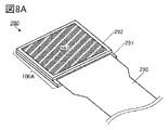
- FIG. 8A and 8B are perspective views showing an example of a display module.
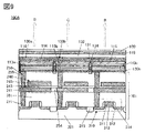
- FIG. 9 is a cross-sectional view showing an example of the display device.
- FIG. 10 is a cross-sectional view showing an example of the display device.
- FIG. 11 is a cross-sectional view showing an example of the display device.
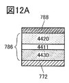
- 12A to 12D are diagrams showing a configuration example of a light emitting device.
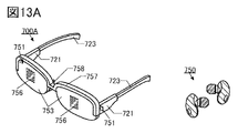
- 13A and 13B are diagrams showing an example of an electronic device.
- 14A and 14B are diagrams showing an example of an electronic device.
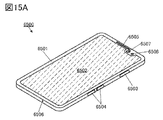
- 15A and 15B are diagrams showing an example of an electronic device.
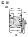
- 16A to 16D are diagrams showing an example of an electronic device.
- 17A to 17F are diagrams showing an example of an electronic device.
- the ordinal numbers “first” and “second” are used for convenience, and limit the number of components or the order of components (for example, process order or stacking order). It's not something to do.
- the ordinal numbers attached to the components in a certain part of the specification may not match the ordinal numbers attached to the components in other parts of the specification or in the claims.
- the word “membrane” and the word “layer” can be interchanged with each other in some cases or depending on the situation.
- the term “conductive layer” can be changed to the term “conductive layer”.
- the term “insulating film” can be changed to the term “insulating layer”.
- a metal mask or a device manufactured by using an FMM may be referred to as a device having an MM (metal mask) structure.
- a device manufactured without using a metal mask or FMM may be referred to as a device having an MML (metal maskless) structure.
- a first layer (EL layer or a part of the EL layer) including a light emitting layer that forms a conductive film and emits light of the first color.
- a first sacrificial layer is formed on the first layer.
- a first resist mask is formed on the first sacrificial layer, and the first layer and the first sacrificial layer are processed by using the first resist mask to form an island-shaped first layer.
- the second layer (which can be said to be the EL layer or a part of the EL layer) including the light emitting layer that emits the light of the second color is referred to as the second sacrificial layer.
- a second resist mask is used to form an island.
- the island-shaped EL layer is not formed by using a fine metal mask, but is processed after forming the EL layer on one surface. Since it is formed, the island-shaped EL layer can be formed with a uniform thickness. Further, by providing the sacrificial layer on the EL layer, it is possible to reduce the damage received by the EL layer during the manufacturing process of the display device and improve the reliability of the light emitting device.
- the pixel electrode After forming the EL layer that emits light of each color, the pixel electrode can be formed by processing the above-mentioned conductive film by using the sacrificial layer remaining on each EL layer as a hard mask. Since it is not necessary to separately provide a mask for forming the pixel electrodes in an island shape, the manufacturing cost of the display device can be reduced. Further, since it is not necessary to provide an insulating layer covering the end portion of the pixel electrode between the pixel electrode and the EL layer, the distance between adjacent light emitting devices can be extremely narrowed. Therefore, it is possible to increase the definition or the resolution of the display device.
- each of the first layer and the second layer includes at least a light emitting layer, and is preferably composed of a plurality of layers. Specifically, it is preferable to have one or more layers on the light emitting layer. By having another layer between the light emitting layer and the sacrificial layer, it is possible to suppress the light emitting layer from being exposed to the outermost surface during the manufacturing process of the display device and reduce the damage to the light emitting layer. As a result, the reliability of the light emitting device can be improved. Therefore, it is preferable that the first layer and the second layer each have a light emitting layer and a carrier transport layer on the light emitting layer.
- the sacrificial layer is removed and the same as the remaining layers constituting the EL layer.
- An electrode (which can also be called an upper electrode) is formed in common for light emitting devices of each color.
- a carrier injection layer and a common electrode can be formed in common for light emitting devices of each color.
- the carrier injection layer is often a layer having relatively high conductivity among the EL layers.
- the light emitting device may be short-circuited. Even when the carrier injection layer is provided in an island shape and the common electrode is formed in common for the light emitting devices of each color, the common electrode and the side surface of the EL layer or the side surface of the pixel electrode are in contact with each other to emit light.
- the device may short-circuit.
- the display device has an island-shaped first carrier transport layer and an island-shaped first carrier transport layer between the island-shaped light emitting layer and the carrier injection layer commonly provided for the light emitting devices of each color. It has two layers with a second carrier transport layer commonly provided in the light emitting device.
- the display device includes a pixel electrode that functions as an anode, an island-shaped hole injection layer, a hole transport layer, a light emitting layer, and a third, which are provided on the pixel electrodes in this order, respectively.
- An electron transport layer, a second electron transport layer provided so as to cover a pixel electrode, a hole injection layer, a hole transport layer, a light emitting layer, and a first electron transport layer, and a second electron. It has an electron injection layer provided on the transport layer and a common electrode provided on the electron injection layer and functioning as a cathode.
- the display device includes a pixel electrode that functions as a cathode, an island-shaped electron injection layer, an electron transport layer, a light emitting layer, and a first, which are provided on the pixel electrodes in this order, respectively.
- a hole transport layer of 1 a second hole transport layer provided so as to cover a pixel electrode, an electron injection layer, an electron transport layer, a light emitting layer, and a first hole transport layer, and a second hole transport layer. It has a hole injection layer provided on the hole transport layer and a common electrode provided on the hole injection layer and functioning as an anode.
- Display device configuration example 1A and 1B show a display device according to an aspect of the present invention.
- FIG. 1A shows a top view of the display device 100.
- the display device 100 has a display unit in which a plurality of pixels 110 are arranged in a matrix, and a connection unit 140 outside the display unit.
- One pixel 110 is composed of three sub-pixels, sub-pixels 110a, 110b, and 110c.
- the connection portion 140 can also be referred to as a cathode contact portion.
- the upper surface shape of the sub-pixel shown in FIG. 1A corresponds to the upper surface shape of the light emitting region.
- the circuit layout constituting the sub-pixels is not limited to the range of the sub-pixels shown in FIG. 1A, and may be arranged outside the sub-pixels.
- the transistor included in the sub-pixel 110a may be located within the range of the sub-pixel 110b shown in FIG. 1A, or part or all of it may be located outside the range of the sub-pixel 110a.
- the aperture ratios (which can also be said to be the size and the size of the light emitting region) of the sub-pixels 110a, 110b, and 110c are shown to be equal or substantially equal, but one aspect of the present invention is not limited thereto.
- the aperture ratios of the sub-pixels 110a, 110b, and 110c can be appropriately determined.
- the aperture ratios of the sub-pixels 110a, 110b, and 110c may be different, respectively, and two or more may be equal or substantially equal.
- FIG. 1A shows an example in which sub-pixels of different colors are arranged side by side in the X direction, and sub-pixels of the same color are arranged side by side in the Y direction.
- the sub-pixels of different colors may be arranged side by side in the Y direction, and the sub-pixels of the same color may be arranged side by side in the X direction.
- FIG. 1A shows an example in which the connecting portion 140 is located below the display portion in a top view, but the present invention is not particularly limited.
- the connecting portion 140 may be provided at at least one of the upper side, the right side, the left side, and the lower side of the display unit in a top view, and may be provided so as to surround the four sides of the display unit.
- FIG. 1B shows a cross-sectional view between the alternate long and short dash lines X1-X2 in FIG. 1A.
- light emitting devices 130a, 130b, and 130c are provided on the layer 101 including the transistor, and protective layers 131, 132 are provided so as to cover these light emitting devices.
- the substrate 120 is bonded to the protective layer 132 by the resin layer 119.
- the display device of one aspect of the present invention is a top emission type (top emission type) that emits light in the direction opposite to the substrate on which the light emitting device is formed, and emits light to the substrate side on which the light emitting device is formed. It may be either a bottom emission type (bottom emission type) or a double-sided emission type (dual emission type) that emits light on both sides.
- the layer 101 including the transistors for example, a laminated structure in which a plurality of transistors are provided on a substrate and an insulating layer is provided so as to cover these transistors can be applied.
- the layer 101 containing the transistor may have a recess between adjacent light emitting devices.
- a recess may be provided in the insulating layer located on the outermost surface of the layer 101 containing the transistor.
- a configuration example of the layer 101 including the transistor will be described later in the second embodiment.
- the light emitting devices 130a, 130b, and 130c each emit light of different colors.
- the light emitting devices 130a, 130b, and 130c are preferably a combination that emits three colors of light, for example, red (R), green (G), and blue (B).
- the light emitting device has an EL layer between the pair of electrodes.
- one of the pair of electrodes may be referred to as a pixel electrode, and the other may be referred to as a common electrode.
- one electrode functions as an anode and the other electrode functions as a cathode.
- the pixel electrode functions as an anode and the common electrode functions as a cathode will be described as an example.
- the light emitting device 130a includes a pixel electrode 111a on a layer 101 containing a transistor, an island-shaped first layer 113a on the pixel electrode 111a, and a fourth electron covering the upper surface and side surfaces of the island-shaped first layer 113a. It has a transport layer 116, an electron injection layer 114 on the fourth electron transport layer 116, and a common electrode 115 on the electron injection layer 114.
- the first layer 113a includes a first hole injection layer 181a on the pixel electrode 111a, a first hole transport layer 182a on the first hole injection layer 181a, and a first hole transport layer 182a.
- first layer 113a the fourth electron transport layer 116, and the electron injection layer 114 can be collectively referred to as an EL layer.
- the light emitting device 130b includes a pixel electrode 111b on a layer 101 containing a transistor, an island-shaped second layer 113b on the pixel electrode 111b, and a fourth electron covering the upper surface and side surfaces of the island-shaped second layer 113b. It has a transport layer 116, an electron injection layer 114 on the fourth electron transport layer 116, and a common electrode 115 on the electron injection layer 114.
- the second layer 113b includes a second hole injection layer 181b on the pixel electrode 111b, a second hole transport layer 182b on the second hole injection layer 181b, and a second hole transport layer 182b.
- the second layer 113b, the fourth electron transport layer 116, and the electron injection layer 114 can be collectively referred to as an EL layer.
- the light emitting device 130c includes a pixel electrode 111c on a layer 101 containing a transistor, an island-shaped third layer 113c on the pixel electrode 111c, and a fourth electron covering the upper surface and side surfaces of the island-shaped third layer 113c. It has a transport layer 116, an electron injection layer 114 on the fourth electron transport layer 116, and a common electrode 115 on the electron injection layer 114.
- the third layer 113c includes a third hole injection layer 181c on the pixel electrode 111c, a third hole transport layer 182c on the third hole injection layer 181c, and a third hole transport layer 182c.
- the third layer 113c, the fourth electron transport layer 116, and the electron injection layer 114 can be collectively referred to as an EL layer.
- the common electrode commonly possessed by the light emitting devices of each color is electrically connected to the conductive layer provided in the connecting portion 140.
- a conductive film that transmits visible light is used for the electrode on the side that extracts light. Further, it is preferable to use a conductive film that reflects visible light for the electrode on the side that does not take out light.
- a metal, an alloy, an electrically conductive compound, a mixture thereof, or the like can be appropriately used as a material for forming the pair of electrodes (pixel electrode and common electrode) of the light emitting device.
- a metal, an alloy, an electrically conductive compound, a mixture thereof, or the like can be appropriately used.
- indium tin oxide also referred to as In-Sn oxide, ITO
- In-Si-Sn oxide also referred to as ITSO
- indium zinc oxide In-Zn oxide
- Al aluminum
- titanium Ti
- Cr chromium
- manganese Mn
- iron Fe
- cobalt Co
- nickel Ni
- copper Cu
- gallium Ga
- zinc zinc
- Indium In
- Molybdenum Mo
- Titanium Ta
- Tungsten W
- Palladium Pd
- Gold Au
- Platinum Pt
- Silver Ag
- Ittrium Y
- Metals such as neodymium (Nd), and alloys containing these in appropriate combinations can also be used.
- a micro-optical resonator (microcavity) structure is applied to the light emitting device. Therefore, one of the pair of electrodes of the light emitting device preferably has an electrode having transparency and reflection to visible light (semi-transmissive / semi-reflective electrode), and the other has an electrode having reflection to visible light (semi-transmissive / semi-reflective electrode). It is preferable to have a reflective electrode).
- the light emitting device has a microcavity structure, the light emitted from the light emitting layer can be resonated between both electrodes, and the light emitted from the light emitting device can be strengthened.
- the semi-transmissive / semi-reflective electrode can have a laminated structure of a reflective electrode and an electrode having transparency to visible light (also referred to as a transparent electrode).
- the light transmittance of the transparent electrode shall be 40% or more.
- an electrode having a transmittance of visible light (light having a wavelength of 400 nm or more and less than 750 nm) of 40% or more as the light emitting device.
- the reflectance of visible light of the semi-transmissive / semi-reflective electrode is 10% or more and 95% or less, preferably 30% or more and 80% or less.
- the reflectance of visible light of the reflecting electrode is 40% or more and 100% or less, preferably 70% or more and 100% or less.
- the resistivity of these electrodes is preferably 1 ⁇ 10 -2 ⁇ cm or less.
- the first layer 113a, the second layer 113b, and the third layer 113c are provided in an island shape, respectively.
- the first layer 113a, the second layer 113b, and the third layer 113c each have a light emitting layer. It is preferable that the first layer 113a, the second layer 113b, and the third layer 113c each have a light emitting layer that emits light of a different color.
- the light emitting layer is a layer containing a light emitting substance.
- the light emitting layer can have one or more kinds of light emitting substances.
- a substance exhibiting a luminescent color such as blue, purple, bluish purple, green, yellowish green, yellow, orange, and red is appropriately used. Further, as the luminescent substance, a substance that emits near-infrared light can also be used.
- luminescent material examples include fluorescent materials, phosphorescent materials, thermally activated delayed fluorescence (TADF) materials, quantum dot materials, and the like.
- fluorescent materials examples include fluorescent materials, phosphorescent materials, thermally activated delayed fluorescence (TADF) materials, quantum dot materials, and the like.
- TADF thermally activated delayed fluorescence
- fluorescent material examples include pyrene derivatives, anthracene derivatives, triphenylene derivatives, fluorene derivatives, carbazole derivatives, dibenzothiophene derivatives, dibenzofuran derivatives, dibenzoquinoxaline derivatives, quinoxalin derivatives, pyridine derivatives, pyrimidine derivatives, phenanthrene derivatives, naphthalene derivatives and the like. Be done.
- an organic metal complex having a 4H-triazole skeleton, a 1H-triazole skeleton, an imidazole skeleton, a pyrimidine skeleton, a pyrazine skeleton, or a pyridine skeleton (particularly an iridium complex), or a phenylpyridine derivative having an electron-withdrawing group is arranged.
- examples thereof include an organic metal complex (particularly an iridium complex), a platinum complex, and a rare earth metal complex as a ligand.
- the light emitting layer may have one or more kinds of organic compounds (host material, assist material, etc.) in addition to the light emitting substance (guest material).
- organic compounds host material, assist material, etc.
- guest material As one or more kinds of organic compounds, one or both of a hole transporting material and an electron transporting material can be used. Further, a bipolar material or a TADF material may be used as one or more kinds of organic compounds.
- the light emitting layer preferably has, for example, a phosphorescent material and a hole transporting material and an electron transporting material which are combinations that easily form an excitation complex.
- ExTET Exciplex-Triplet Energy Transfer
- a combination that forms an excitation complex that emits light that overlaps the wavelength of the absorption band on the lowest energy side of the luminescent substance energy transfer becomes smooth and light emission can be obtained efficiently.
- high efficiency, low voltage drive, and long life of the light emitting device can be realized at the same time.
- the first layer 113a, the second layer 113b, and the third layer 113c are layers other than the light emitting layer, such as a substance having a high hole injection property, a substance having a high hole transport property, a hole blocking material, and an electron. It may further have a layer containing a highly transportable substance, a highly electron-injectable substance, an electron blocking material, a bipolar substance (a substance having a high electron transport property and a hole transport property), and the like.
- Either a low molecular weight compound or a high molecular weight compound can be used as the light emitting device, and an inorganic compound may be contained.
- the layers constituting the light emitting device can be formed by a vapor deposition method (including a vacuum vapor deposition method), a transfer method, a printing method, an inkjet method, a coating method, or the like.
- the first layer 113a, the second layer 113b, and the third layer 113c are a hole injection layer, a hole transport layer, a hole block layer, an electron block layer, an electron transport layer, and an electron, respectively. It may have one or more of the injection layers.
- one of the hole injection layer, the hole transport layer, the hole block layer, the electron block layer, the electron transport layer, and the electron injection layer is formed in common with the light emitting devices of each color. One or more can be applied.
- the first layer 113a has a first light emitting layer 183a and a first electron transport layer 184a on the first light emitting layer 183a.
- the second layer 113b has a second light emitting layer 183b and a second electron transport layer 184b on the second light emitting layer 183b
- the third layer 113c has a third light emitting layer. It has a layer 183c and a third electron transport layer 184c on the third light emitting layer 183c.
- the first layer 113a, the second layer 113b, and the third layer 113c are covered with the fourth electron transport layer 116, and the electron injection layer 114 and the common electrode are placed on the fourth electron transport layer 116. 115 is provided.
- the electron injection layer 114 or the common electrode 115 comes into contact with the side surfaces of the pixel electrodes 111a, 111b, 111c, and the first layer 113a, the second layer 113b, and the third layer 113c. Can be suppressed and a short circuit of the light emitting device can be suppressed.
- the hole injection layer is a layer for injecting holes from the anode into the hole transport layer, and is a layer containing a material having high hole injectability.
- the material having high hole injectability include an aromatic amine compound and a composite material containing a hole transporting material and an acceptor material (electron accepting material).
- the hole transport layer is a layer that transports holes injected from the anode to the light emitting layer by the hole injection layer.
- the hole transport layer is a layer containing a hole transport material.
- a hole transporting material a substance having a hole mobility of 1 ⁇ 10-6 cm 2 / Vs or more is preferable. In addition, any substance other than these can be used as long as it is a substance having a higher hole transport property than electrons.
- the hole-transporting material include materials having high hole-transporting properties such as ⁇ -electron-rich heteroaromatic compounds (for example, carbazole derivatives, thiophene derivatives, furan derivatives, etc.) and aromatic amines (compounds having an aromatic amine skeleton). Is preferable.
- the electron transport layer is a layer that transports electrons injected from the cathode to the light emitting layer by the electron injection layer.
- the electron transport layer is a layer containing an electron transport material.
- As the electron transporting material a substance having an electron mobility of 1 ⁇ 10-6 cm 2 / Vs or more is preferable. In addition, any substance other than these can be used as long as it is a substance having a higher electron transport property than holes.
- Examples of the electron-transporting material include a metal complex having a quinoline skeleton, a metal complex having a benzoquinolin skeleton, a metal complex having an oxazole skeleton, a metal complex having a thiazole skeleton, and the like, as well as oxadiazole derivatives, triazole derivatives, and imidazole derivatives.
- Materials with high electron transport properties such as deficient heterocyclic compounds can be used.
- the electron injection layer is a layer for injecting electrons from the cathode into the electron transport layer, and is a layer containing a material having high electron injectability.
- a material having high electron injectability an alkali metal, an alkaline earth metal, or a compound thereof can be used.
- a composite material containing an electron transporting material and a donor material (electron donating material) can also be used.
- Examples of the electron injection layer include lithium, cesium, lithium fluoride (LiF), cesium fluoride (CsF), calcium fluoride (CaF 2 ), 8- (quinolinolato) lithium (abbreviation: Liq), 2- (2). -Pyridyl) phenolatrithium (abbreviation: LiPP), 2- (2-pyridyl) -3-pyridinolatolithium (abbreviation: LiPPy), 4-phenyl-2- (2-pyridyl) phenolatrithium (abbreviation: LiPPP) , Lithium oxide (LiO x ), alkali metals such as cesium carbonate, alkaline earth metals, or compounds thereof can be used.
- an electron transporting material may be used as the electron injection layer.
- a compound having an unshared electron pair and an electron-deficient heteroaromatic ring can be used as an electron transporting material.
- a compound having at least one of a pyridine ring, a diazine ring (pyrimidine ring, pyrazine ring, pyridazine ring), and a triazine ring can be used.
- the lowest empty orbital (LUMO: Lowest Unellad Molecular Orbital) of the organic compound having an unshared electron pair is preferably -3.6 eV or more and -2.3 eV or less.
- the highest occupied orbital (HOMO: Highest Occupied Molecular Orbital) level and LUMO level of an organic compound are determined by CV (cyclic voltammetry), photoelectron spectroscopy, photoabsorption spectroscopy, back-photoelectron spectroscopy, etc. Can be estimated.
- BPhen 4,7-diphenyl-1,10-phenanthroline
- NBPhen 2,9-bis (naphthalene-2-yl) -4,7-diphenyl-1,10-phenanthroline
- diquinoxalino [2,3-a: 2', 3'-c] Phenazine (abbreviation: HATNA), 2,4,6-tris [3'-(pyridin-3-yl) biphenyl-3-yl] -1,3 , 5-Triazine (abbreviation: TmPPPyTZ) and the like can be used for organic compounds having unshared electron pairs.
- Tg glass transition temperature
- Tg glass transition temperature
- the protective layers 131 and 132 are on the light emitting devices 130a, 130b and 130c. By providing the protective layers 131 and 132, the reliability of the light emitting device can be improved.
- the conductivity of the protective layers 131 and 132 does not matter.
- As the protective layers 131 and 132 at least one of an insulating film, a semiconductor film, and a conductive film can be used.
- Deterioration of the light emitting device such as preventing oxidation of the common electrode 115 by having the protective layers 131 and 132 having an inorganic film, and suppressing impurities (moisture, oxygen, etc.) from entering the light emitting devices 130a, 130b, 130c. Can be suppressed and the reliability of the display device can be improved.
- an inorganic insulating film such as an oxide insulating film, a nitride insulating film, an oxide nitride insulating film, and a nitride oxide insulating film can be used.
- the oxide insulating film include a silicon oxide film, an aluminum oxide film, a gallium oxide film, a germanium oxide film, an yttrium oxide film, a zirconium oxide film, a lanthanum oxide film, a neodymium oxide film, a hafnium oxide film, and a tantalum oxide film. ..
- Examples of the nitride insulating film include a silicon nitride film and an aluminum nitride film.
- Examples of the oxide nitride insulating film include a silicon nitride film and an aluminum nitride film.
- Examples of the nitriding insulating film include a silicon nitriding film and an aluminum nitriding film.
- the oxide nitride refers to a material having a higher oxygen content than nitrogen in its composition, and the nitride oxide has a higher nitrogen content than oxygen in its composition. Refers to the material.
- the protective layers 131 and 132 preferably have a nitride insulating film or a nitride oxide insulating film, respectively, and more preferably have a nitride insulating film.
- In-Sn oxide also referred to as ITO
- In-Zn oxide Ga-Zn oxide
- Al-Zn oxide indium gallium zinc oxide
- In-Ga- indium gallium zinc oxide
- An inorganic film containing Zn oxide also referred to as IGZO or the like can also be used.
- the inorganic film preferably has a high resistance, and specifically, the inorganic film preferably has a higher resistance than the common electrode 115.
- the inorganic film may further contain nitrogen.
- the protective layers 131 and 132 When the light emitted from the light emitting device is taken out through the protective layers 131 and 132, the protective layers 131 and 132 preferably have high transparency to visible light.
- the protective layers 131 and 132 preferably have high transparency to visible light.
- ITO, IGZO, and aluminum oxide are preferable because they are inorganic materials having high transparency to visible light.
- Examples of the protective layers 131 and 132 include a laminated structure of an aluminum oxide film and a silicon nitride film on an aluminum oxide film, or a laminated structure of an aluminum oxide film and an IGZO film on an aluminum oxide film. Can be used. By using the laminated structure, it is possible to prevent impurities (water, oxygen, etc.) from entering the EL layer side.
- the protective layers 131 and 132 may have an organic film.
- the protective layer 132 may have both an organic film and an inorganic film.
- the protective layer 131 and the protective layer 132 may be formed by using an atomic layer deposition (ALD) method, and the protective layer 132 may be formed by using a sputtering method.
- ALD atomic layer deposition
- the respective ends of the pixel electrodes 111a, 111b, and 111c are not covered with an insulating layer. Therefore, the distance between adjacent light emitting devices can be extremely narrowed. Therefore, it can be a high-definition or high-resolution display device.
- light emitting layers of each color are provided in an island shape for each light emitting device, and are manufactured by a so-called separate painting method (SBS (Side By Side) method). Therefore, it is possible to realize a display device having high light extraction efficiency as compared with a configuration in which a white light emitting device and a color filter are combined. Further, since a single-structured light-emitting device can be applied, a display device having a lower drive voltage can be realized as compared with a configuration using a tandem-structured light-emitting device.
- SBS Standard By Side
- the SBS method it is possible to realize a display device having low power consumption as compared with a configuration in which a light emitting device for white light emission and a color filter are combined and a configuration in which a light emitting device having a tandem structure is used.
- the display device of the present embodiment can reduce the distance between the light emitting devices.
- the distance between the light emitting devices is 1 ⁇ m or less, preferably 500 nm or less, more preferably 200 nm or less, 100 nm or less, 90 nm or less, 70 nm or less, 50 nm or less, 30 nm or less, 20 nm or less, 15 nm or less, or 10 nm. It can be as follows. In other words, there is a region where the distance between the side surface of the first layer 113a and the side surface of the second layer 113b, or the distance between the side surface of the second layer 113b and the side surface of the third layer 113c is 1 ⁇ m or less. It has a region of 0.5 ⁇ m (500 nm) or less, and more preferably a region of 100 nm or less.
- a light-shielding layer may be provided on the surface of the substrate 120 on the resin layer 119 side.
- various optical members can be arranged on the outside of the substrate 120.
- the optical member include a polarizing plate, a retardation plate, a light diffusing layer (diffusing film, etc.), an antireflection layer, a condensing film, and the like.
- an antistatic film for suppressing the adhesion of dust, a water-repellent film for preventing the adhesion of dirt, a hardcoat film for suppressing the occurrence of scratches due to use, a shock absorbing layer and the like are arranged. You may.
- the substrate 120 glass, quartz, ceramic, sapphire, resin, metal, alloy, semiconductor and the like can be used.
- a material that transmits the light is used for the substrate on the side that extracts the light from the light emitting device.
- a flexible material is used for the substrate 120, the flexibility of the display device can be increased and a flexible display can be realized.
- a polarizing plate may be used as the substrate 120.
- the substrate 120 examples include polyester resins such as polyethylene terephthalate (PET) and polyethylene naphthalate (PEN), polyacrylonitrile resins, acrylic resins, polyimide resins, polymethylmethacrylate resins, polycarbonate (PC) resins, and polyether sulfone (PES) resins. , Polyamide resin (nylon, aramid, etc.), polysiloxane resin, cycloolefin resin, polystyrene resin, polyamideimide resin, polyurethane resin, polyvinyl chloride resin, polyvinylidene chloride resin, polypropylene resin, polytetrafluoroethylene (PTFE) resin, ABS resin, cellulose nanofibers and the like can be used. Glass having a thickness sufficient to have flexibility may be used for the substrate 120.
- PET polyethylene terephthalate
- PEN polyethylene naphthalate
- PES polyether sulfone
- Polyamide resin nylon, aramid, etc.
- a substrate having high optical isotropic properties has a small amount of birefringence (it can be said that the amount of birefringence is small).
- the absolute value of the retardation (phase difference) value of the substrate having high optical isotropic properties is preferably 30 nm or less, more preferably 20 nm or less, still more preferably 10 nm or less.
- the film having high optical isotropic properties examples include a triacetyl cellulose (TAC, also referred to as cellulose triacetate) film, a cycloolefin polymer (COP) film, a cycloolefin copolymer (COC) film, and an acrylic film.
- TAC triacetyl cellulose
- COP cycloolefin polymer
- COC cycloolefin copolymer
- a film having a low water absorption rate as the substrate.
- a film having a water absorption rate of 1% or less more preferably a film having a water absorption rate of 0.1% or less, and further preferably using a film having a water absorption rate of 0.01% or less.
- various curable adhesives such as a photocurable adhesive such as an ultraviolet curable adhesive, a reaction curable adhesive, a thermosetting adhesive, and an anaerobic adhesive can be used.
- these adhesives include epoxy resin, acrylic resin, silicone resin, phenol resin, polyimide resin, imide resin, PVC (polyvinyl chloride) resin, PVB (polyvinyl butyral) resin, EVA (ethylene vinyl acetate) resin and the like.
- a material having low moisture permeability such as epoxy resin is preferable.
- a two-component mixed type resin may be used.
- FIG. 1B shows an example in which the insulating material 134 is filled in a portion that may be a gap.
- the voids are not formed and it is not necessary to fill the insulator 134. In some cases.
- the structure is such that at least one of the fourth electron transport layer 116 and the electron injection layer 114 is filled between the adjacent light emitting devices.
- the voids have, for example, one or more selected from air, nitrogen, oxygen, carbon dioxide, and Group 18 elements (typically helium, neon, argon, xenon, krypton, etc.). Further, the void may contain, for example, a gas used for forming the electron injection layer 114. For example, when the electron injection layer 114 is formed by the vacuum vapor deposition method, the voids may have a reduced pressure atmosphere. When a gas is contained in the void, the gas can be identified by a gas chromatography method or the like.
- the refractive index of the void is lower than the refractive index of the fourth electron transport layer 116
- the light emitted from the first layer 113a, the second layer 113b, or the third layer 113c is the fourth electron. Reflects at the interface between the transport layer 116 and the voids.
- the material of the insulator 134 that can be filled in the portion that may be a gap one or both of the organic insulating material and the inorganic insulating material can be used. At least one of a solid substance, a gel-like substance, and a liquid substance can be used for the insulator 134.
- organic insulating material examples include acrylic resin, epoxy resin, polyimide resin, polyamide resin, polyimideamide resin, polysiloxane resin, benzocyclobutene resin, and phenol resin. Further, various resins that can be used for the resin layer 119 may be used.
- the inorganic insulating material examples include an oxide insulating material, a nitride insulating material, an oxide nitride insulating material, and an oxide insulating material. Further, an insulating material that can be used for the protective layers 131 and 132 may be used.
- Materials that can be used for conductive layers such as transistor gates, sources and drains, as well as various wirings and electrodes that make up display devices include aluminum, titanium, chromium, nickel, copper, yttrium, zirconium, molybdenum, and silver. Examples thereof include metals such as titanium and tungsten, and alloys containing the metal as a main component. A film containing these materials can be used as a single layer or as a laminated structure.
- a conductive oxide such as indium oxide, indium tin oxide, indium zinc oxide, zinc oxide, zinc oxide containing gallium, or graphene can be used.
- a metal material such as gold, silver, platinum, magnesium, nickel, tungsten, chromium, molybdenum, iron, cobalt, copper, palladium, and titanium, or an alloy material containing the metal material can be used.
- a nitride of the metal material for example, titanium nitride
- the laminated film of the above material can be used as the conductive layer.
- a laminated film of an alloy of silver and magnesium and an indium tin oxide because the conductivity can be enhanced.
- These can also be used for conductive layers such as various wirings and electrodes constituting the display device, and conductive layers (conductive layers that function as pixel electrodes or common electrodes) of the light emitting device.
- Examples of the insulating material that can be used for each insulating layer include resins such as acrylic resin and epoxy resin, and inorganic insulating materials such as silicon oxide, silicon oxide, silicon nitride, silicon nitride, and aluminum oxide.
- FIGS. 2 to 7. are top views showing a method of manufacturing a display device.
- 3A to 3C show a cross-sectional view between the alternate long and short dash lines X1-X2 and a cross-sectional view between Y1-Y2 in FIG. 1A side by side.
- FIGS. 4 to 7 show a cross-sectional view between the alternate long and short dash lines X1-X2 and a cross-sectional view between Y1-Y2 in FIG. 1A side by side. The same applies to FIGS. 4 to 7 as in FIG.
- the thin films (insulating film, semiconductor film, conductive film, etc.) constituting the display device are formed by a sputtering method, a chemical vapor deposition (CVD) method, a vacuum deposition method, and a pulsed laser deposition (PLD). ) Method, ALD method, etc. can be used for formation.
- CVD method include a plasma chemical vapor deposition (PECVD: Plasma Enhanced CVD) method and a thermal CVD method.
- PECVD plasma chemical vapor deposition
- thermal CVD there is an organometallic chemical vapor deposition (MOCVD: Metal Organic CVD) method.
- the thin films (insulating film, semiconductor film, conductive film, etc.) constituting the display device include spin coating, dip, spray coating, inkjet, dispense, screen printing, offset printing, doctor knife, slit coating, roll coating, etc. It can be formed by a method such as a curtain coat or a knife coat.
- a vacuum process such as a vapor deposition method and a solution process such as a spin coating method and an inkjet method can be used for manufacturing the light emitting device.
- the vapor deposition method include a physical vapor deposition method (PVD method) such as a sputtering method, an ion plating method, an ion beam vapor deposition method, a molecular beam vapor deposition method, and a vacuum vapor deposition method, and a chemical vapor deposition method (CVD method).
- PVD method physical vapor deposition method
- CVD method chemical vapor deposition method
- a vapor deposition method vacuum vapor deposition method, etc.
- a coating method dip coating method, etc.
- printing method ink-film deposition method, screen (stencil printing) method, offset (lithographic printing) method, flexo (lithographic printing) method, gravure method, or micro It can be formed by a method such as the contact method).
- the thin film when processing the thin film constituting the display device, a photolithography method or the like can be used.
- the thin film may be processed by a nanoimprint method, a sandblast method, a lift-off method, or the like.
- the island-shaped thin film may be directly formed by a film forming method using a shielding mask such as a metal mask.
- a photolithography method there are typically the following two methods.
- One is a method of forming a resist mask on a thin film to be processed, processing the thin film by etching or the like, and removing the resist mask.
- the other is a method in which a photosensitive thin film is formed and then exposed and developed to process the thin film into a desired shape.
- the light used for exposure for example, i-line (wavelength 365 nm), g-line (wavelength 436 nm), h-line (wavelength 405 nm), or a mixture of these can be used.
- ultraviolet rays, KrF laser light, ArF laser light, or the like can also be used.
- the exposure may be performed by the immersion exposure technique.
- extreme ultraviolet (EUV: Extreme Ultra-violet) light or X-rays may be used.
- an electron beam can be used instead of the light used for exposure. It is preferable to use extreme ultraviolet light, X-rays, or an electron beam because extremely fine processing is possible.
- extreme ultraviolet light, X-rays, or an electron beam because extremely fine processing is possible.
- a dry etching method, a wet etching method, a sandblasting method, or the like can be used for etching the thin film.
- the conductive film 111 is formed on the layer 101 containing the transistor.
- the first hole injection layer 181A, the first hole transport layer 182A, the first light emitting layer 183A, and the first electron transport layer 184A are formed on the conductive film 111 in this order, and the first A first sacrificial layer 118A is formed on the electron transport layer 184A.
- FIG. 3A in the cross-sectional view between Y1 and Y2, the first hole injection layer 181A, the first hole transport layer 182A, the first light emitting layer 183A, and the first electron transport layer 184A.
- the end on the connecting portion 140 side is located inside the end of the first sacrificial layer 118A.
- the first hole injection layer 181A and the first hole transport The region formed by the layer 182A, the first light emitting layer 183A, the first electron transport layer 184A, and the first sacrificial layer 118A can be changed.
- the light emitting device is formed by using a resist mask, but by combining with the area mask as described above, the light emitting device can be manufactured by a relatively simple process.
- the conductive film 111 is a layer that becomes the pixel electrodes 111a, 111b, 111c, and the conductive layer 123 by being processed later. Therefore, the configuration applicable to the pixel electrode described above can be applied to the conductive film 111.
- a sputtering method or a vacuum vapor deposition method can be used for the formation of the conductive film 111.
- the first hole injection layer 181A, the first hole transport layer 182A, the first light emitting layer 183A, and the first electron transport layer 184A are later described as the first hole injection layer 181a and the first hole transport layer 184A, respectively.
- the hole transport layer 182a, the first light emitting layer 183a, and the first electron transport layer 184a are later described as the first hole injection layer 181a and the first hole transport layer 184A, respectively.
- the hole transport layer 182a, the first light emitting layer 183a, and the first electron transport layer 184a are later described as the first hole injection layer 181a and the first hole transport layer 184A, respectively.
- the hole transport layer 182a, the first light emitting layer 183a, and the first electron transport layer 184a can be applied, respectively.
- the first hole injection layer 181A, the first hole transport layer 182A, the first light emitting layer 183A, and the first electron transport layer 184A are each formed by a vapor deposition method (including a vacuum vapor deposition method), a transfer method, and the like. It can be formed by a printing method, an inkjet method, a coating method, or the like. Further, the first hole injection layer 181A, the first hole transport layer 182A, the first light emitting layer 183A, and the first electron transport layer 184A may each be formed by using a premix material. ..
- the first sacrificial layer 118A is formed with a first hole injection layer 181A, a first hole transport layer 182A, a first light emitting layer 183A, a first electron transport layer 184A, and a later step.
- the first sacrificial layer 118A may have a single-layer structure or a laminated structure.
- the first sacrificial layer 118A for example, a sputtering method, an ALD method (including a thermal ALD method and a PEALD method), or a vacuum deposition method can be used.
- a forming method with less damage to the EL layer is preferable, and the first sacrificial layer 118A is preferably formed by using an ALD method or a vacuum vapor deposition method rather than a sputtering method.
- the first sacrificial layer 118A it is preferable to use a film that can be removed by a wet etching method.
- a wet etching method By using the wet etching method, the first hole injection layer 181A, the first hole transport layer 182A, and the first light emission during processing of the first sacrificial layer 118A, as compared with the case where the dry etching method is used. It is possible to reduce the damage applied to the layer 183A and the first electron transport layer 184A.
- an inorganic film such as a metal film, an alloy film, a metal oxide film, a semiconductor film, or an inorganic insulating film can be used.
- the first sacrificial layer 118A includes, for example, a metal material such as gold, silver, platinum, magnesium, nickel, tungsten, chromium, molybdenum, iron, cobalt, copper, palladium, titanium, aluminum, yttrium, zirconium, and tantalum, or An alloy material containing the metal material can be used.
- a metal material such as gold, silver, platinum, magnesium, nickel, tungsten, chromium, molybdenum, iron, cobalt, copper, palladium, titanium, aluminum, yttrium, zirconium, and tantalum, or An alloy material containing the metal material can be used.
- a metal oxide such as In-Ga-Zn oxide can be used for the first sacrificial layer 118A.
- an In-Ga-Zn oxide film can be formed by using a sputtering method.
- indium oxide, In-Zn oxide, In-Sn oxide, indium titanium oxide (In-Ti oxide), indium tin zinc oxide (In-Sn-Zn oxide), indium titanium zinc oxide ( In-Ti-Zn oxide), indium gallium tin zinc oxide (In-Ga-Sn-Zn oxide) and the like can be used.
- indium tin oxide containing silicon or the like can also be used.
- the element M is aluminum, silicon, boron, yttrium, copper, vanadium, beryllium, titanium, iron, nickel, germanium, zirconium, molybdenum, lanthanum, cerium, neodymium, hafnium, tantalum, tungsten). , Or one or more selected from magnesium).
- the first sacrificial layer 118A various inorganic insulating films that can be used for the protective layers 131 and 132 can be used.
- the oxide insulating film is preferable because it has higher adhesion to the EL layer than the nitride insulating film.
- an inorganic insulating material such as aluminum oxide, hafnium oxide, or silicon oxide can be used for the first sacrificial layer 118A.
- the ALD method can be used to form an aluminum oxide film. It is preferable to use the ALD method because damage to the base (particularly the EL layer) can be reduced.
- a resist mask 190a is formed on the first sacrificial layer 118A.
- the resist mask can be formed by applying a photosensitive resin (photoresist), exposing and developing the mask.
- the resist mask 190a is provided at a position overlapping the region that will later become the sub-pixel 110a. Further, it is preferable that the resist mask 190a is also provided at a position overlapping the region that will later become the connecting portion 140. As a result, it is possible to prevent the region of the conductive film 111 that will later become the conductive layer 123 from being damaged during the manufacturing process of the display device.
- the resist mask 190a it is preferable that one island-shaped pattern is provided for one sub-pixel 110a.
- one band-shaped pattern may be formed for a plurality of sub-pixels 110a arranged in a row (arranged in the Y direction in FIG. 2A).
- the first hole injection layer 181a, the first hole transport layer 182a, the first light emitting layer 183a, and the first electron transport layer 184a are placed on the conductive film 111.
- the laminated structure of the first sacrificial layer 118a and the resist mask 190a remains.
- a laminated structure of the first sacrificial layer 118a and the resist mask 190a remains on the conductive film 111.
- the laminated structure of the first hole injection layer 181a, the first hole transport layer 182a, the first light emitting layer 183a, and the first electron transport layer 184a is also referred to as the first layer 113a.
- the resist mask 190a is removed.
- the first sacrificial layer 118A can be processed by a wet etching method or a dry etching method.
- the processing of the first sacrificial layer 118A is preferably performed by anisotropic etching.
- the wet etching method By using the wet etching method, the first hole injection layer 181A, the first hole transport layer 182A, and the first light emission during processing of the first sacrificial layer 118A, as compared with the case where the dry etching method is used. It is possible to reduce the damage applied to the layer 183A and the first electron transport layer 184A.
- a developing solution an aqueous solution of tetramethylammonium hydroxide (TMAH), dilute phosphoric acid, oxalic acid, phosphoric acid, acetic acid, nitric acid, or a chemical solution using a mixed solution thereof may be used. preferable.
- the dry etching method when used, by not using a gas containing oxygen as the etching gas, the first hole injection layer 181A, the first hole transport layer 182A, the first light emitting layer 183A, and the like. Deterioration of the first electron transport layer 184A can be suppressed.
- a gas containing a noble gas also referred to as a noble gas
- FIG. 3C With the resist mask 190a left, the first hole injection layer 181A, the first hole transport layer 182A, the first light emitting layer 183A, and the first electron transport layer 184A, An example of processing the first sacrificial layer 118A is shown, but the present invention is not limited to this.
- the first sacrificial layer 118A has a laminated structure, a part of the layers is processed by using the resist mask 190a, the resist mask 190a is removed, and then the part of the layers is used as a hard mask and the rest. Layer may be processed.
- the resist mask 190a is removed by ashing using oxygen plasma or the like.
- the remaining layer of the first sacrificial layer 118A is located on the outermost surface, and the first hole injection layer 181A, the first hole transport layer 182A, the first light emitting layer 183A, and the first Since the electron transport layer 184A is not exposed, the first hole injection layer 181A, the first hole transport layer 182A, the first light emitting layer 183A, and the first electron in the process of removing the resist mask 190a. It is possible to prevent damage to the transport layer 184A.
- first sacrificial layer 118A is used as a hard mask, and the remaining layers of the first sacrificial layer 118A, the first hole injection layer 181A, and the first hole transport are used.
- the layer 182A, the first light emitting layer 183A, and the first electron transport layer 184A can be processed, respectively.
- the processing of the first hole injection layer 181A, the first hole transport layer 182A, the first light emitting layer 183A, and the first electron transport layer 184A is preferably performed by anisotropic etching.
- anisotropic dry etching is preferable.
- the etching gas it is preferable to use a gas containing nitrogen, a gas containing hydrogen, a gas containing noble gas, a gas containing nitrogen and argon, a gas containing nitrogen and hydrogen, and the like. By not using a gas containing oxygen as the etching gas, deterioration of the first hole injection layer 181A, the first hole transport layer 182A, the first light emitting layer 183A, and the first electron transport layer 184A can be prevented. It can be suppressed.
- a gas containing oxygen may be used as the etching gas. Since the etching gas contains oxygen, the etching speed can be increased. Therefore, it is possible to perform etching under low power conditions while maintaining a sufficient etching rate. Therefore, damage to the first hole injection layer 181A, the first hole transport layer 182A, the first light emitting layer 183A, and the first electron transport layer 184A can be suppressed. Further, it is possible to suppress problems such as adhesion of reaction products that occur during etching.
- the second hole injection layer 181B, the second hole transport layer 182B, the second light emitting layer 183B, and the second electron transport layer 184B is located inside the end of the second sacrificial layer 118B.
- the second hole injection layer 181B, the second hole transport layer 182B, the second light emitting layer 183B, and the second electron transport layer 184B were later introduced into the second hole injection layer 181b and the second, respectively.
- the second light emitting layer 183b emits light of a color different from that of the first light emitting layer 183a.
- the configurations and materials applicable to the second hole injection layer 181b, the second hole transport layer 182b, the second light emitting layer 183b, and the second electron transport layer 184b are the first hole injection, respectively.
- the second hole transport layer 182B, the second light emitting layer 183B, and the second electron transport layer 184B are the first hole injection layer 181A, the first hole transport layer 182A, and the first light emission, respectively.
- the film can be formed by the same method as the layer 183A and the first electron transport layer 184A.
- the second sacrificial layer 118B can be formed using a material applicable to the first sacrificial layer 118A.
- a resist mask 190b is formed on the second sacrificial layer 118B.
- the resist mask 190b is provided at a position overlapping the region that will later become the sub-pixel 110b. Further, it is preferable that the resist mask 190b is also provided at a position overlapping the region that will later become the connecting portion 140. As a result, it is possible to prevent the region of the conductive film 111 that will later become the conductive layer 123 from being damaged during the manufacturing process of the display device. If the first sacrificial layer 118a is provided in the region that will later become the connecting portion 140, the resist mask 190b may not be provided in the region. As the resist mask 190b, it is preferable that one island-shaped pattern is provided for one sub-pixel 110b. Alternatively, as the resist mask 190b, one band-shaped pattern may be formed for a plurality of sub-pixels 110b arranged in a row.
- the second hole injection layer 181b, the second hole transport layer 182b, the second light emitting layer 183b, and the second electron transport layer 184b are placed on the conductive film 111.
- the laminated structure of the second sacrificial layer 118b and the resist mask 190b remains.
- the laminated structure of the first sacrificial layer 118a, the second sacrificial layer 118b, and the resist mask 190b remains on the conductive film 111.
- the laminated structure of the second hole injection layer 181b, the second hole transport layer 182b, the second light emitting layer 183b, and the second electron transport layer 184b is also referred to as the second layer 113b. After that, the resist mask 190b is removed.
- the second sacrificial layer 118B can be processed using a method applicable to the processing of the first sacrificial layer 118A.
- the second hole injection layer 181B, the second hole transport layer 182B, the second light emitting layer 183B, and the second electron transport layer 184B are the first hole injection layer 181A and the first hole transport. It can be processed using a method applicable to the processing of the layer 182A, the first light emitting layer 183A, and the first electron transport layer 184A.
- the resist mask 190b can be removed by a method and timing applicable to the removal of the resist mask 190a.
- the third hole injection layer 181C, the third hole transport layer 182C, The third light emitting layer 183C and the third electron transporting layer 184C are formed in this order, and the third sacrificial layer 118C is formed on the third electron transporting layer 184C.
- the third hole injection layer 181C, the third hole transport layer 182C, the third light emitting layer 183C, and the third electron transport layer 184C is located inside the end of the third sacrificial layer 118C.
- the third hole injection layer 181C, the third hole transport layer 182C, the third light emitting layer 183C, and the third electron transport layer 184C were later described as the third hole injection layer 181c and the third hole transport layer 181c, respectively.
- the third light emitting layer 183c emits light having a color different from that of the first light emitting layer 183a and the second light emitting layer 183b.
- the configurations and materials applicable to the third hole injection layer 181c, the third hole transport layer 182c, the third light emitting layer 183c, and the third electron transport layer 184c are the first hole injection, respectively.
- the third hole injection layer 181C, the third hole transport layer 182C, the third light emitting layer 183C, and the third electron transport layer 184C are the first hole injection layer 181A and the first positive, respectively.
- a film can be formed using the same method as the hole transport layer 182A, the first light emitting layer 183A, and the first electron transport layer 184A.
- the third sacrificial layer 118C can be formed using a material applicable to the first sacrificial layer 118A.
- a resist mask 190c is formed on the third sacrificial layer 118C.
- the resist mask 190c is provided at a position overlapping the region that will later become the sub-pixel 110c.
- the resist mask 190c it is preferable that one island-shaped pattern is provided for one sub-pixel 110c.
- one band-shaped pattern may be formed for a plurality of sub-pixels 110c arranged in a row.
- the resist mask 190c is also provided at a position overlapping the region that will later become the connecting portion 140. If at least one of the first sacrificial layer 118a and the second sacrificial layer 118b is provided in the region to be the connecting portion 140 later, the resist mask 190c may not be provided in the region.
- the third hole injection layer 181c, the third hole transport layer 182c, the third light emitting layer 183c, and the third electron transport layer 184c are placed on the conductive film 111.
- the laminated structure of the third sacrificial layer 118c and the resist mask 190c remains.
- a laminated structure of the first sacrificial layer 118a, the second sacrificial layer 118b, the third sacrificial layer 118c, and the resist mask 190c remains on the conductive film 111.
- the laminated structure of the third hole injection layer 181c, the third hole transport layer 182c, the third light emitting layer 183c, and the third electron transport layer 184c is also referred to as the third layer 113c. Then, as shown in FIG. 6A, the resist mask 190c is removed.
- the third sacrificial layer 118C can be processed using a method applicable to the processing of the first sacrificial layer 118A.
- the third hole injection layer 181C, the third hole transport layer 182C, the third light emitting layer 183C, and the third electron transport layer 184C are the first hole injection layer 181A and the first hole transport. It can be processed using a method applicable to the processing of the layer 182A, the first light emitting layer 183A, and the first electron transport layer 184A.
- the resist mask 190c can be removed by a method and timing applicable to the removal of the resist mask 190a.
- the conductive film 111 is processed by using the first sacrificial layer 118a, the second sacrificial layer 118b, and the third sacrificial layer 118c as a hard mask, and the pixel electrodes 111a, The 111b, 111c, and the conductive layer 123 are formed.
- a part of the layer 101 including the transistor (specifically, the insulating layer located on the outermost surface) may be processed to form a recess.
- the layer 101 including the transistor is provided with a recess will be described as an example, but the recess may not be provided.
- At least a third sacrificial layer 118c may be provided at the connecting portion 140.
- the laminated structure of the second sacrificial layer 118b and the third sacrificial layer 118c, or the laminated structure of the first sacrificial layer 118a, the second sacrificial layer 118b, and the third sacrificial layer 118c. Is preferable because the region of the conductive film 111 that becomes the conductive layer 123 can be prevented from being damaged during the manufacturing process of the display device.
- the conductive film 111 can be processed by a wet etching method or a dry etching method.
- the conductive film 111 is preferably processed by anisotropic etching.
- the first sacrificial layer 118a, the second sacrificial layer 118b, and the third sacrificial layer 118c are removed.
- the first electron transport layer 184a is exposed on the pixel electrode 111a
- the second electron transport layer 184b is exposed on the pixel electrode 111b
- the third electron transport layer 184c is exposed on the pixel electrode 111c.
- the conductive layer 123 is exposed.
- the same method as the step of processing the sacrificial layer can be used.
- the first sacrificial layer 118a, the second sacrificial layer 118b, and the third sacrificial layer 118c are removed as compared with the case where the dry etching method is used.
- the damage applied to the layer 113a, the second layer 113b, and the third layer 113c can be reduced.
- a fourth electron transport layer 116 is formed so as to cover the first layer 113a, the second layer 113b, and the third layer 113c.
- the end of the fourth electron transport layer 116 on the connection portion 140 side is located inside the connection portion 140, and the conductive layer 123 remains exposed. Is.
- the materials that can be used as the fourth electron transport layer 116 are as described above.
- the fourth electron transport layer 116 can be formed by a method such as a thin film deposition method (including a vacuum vapor deposition method), a transfer method, a printing method, an inkjet method, or a coating method. Further, the fourth electron transport layer 116 may be formed by using a premix material.
- the fourth electron transport layer 116 is formed by using a material having a higher insulating property than the electron injection layer 114 to be formed next.
- the fourth electron transport layer 116 is provided so as to cover the upper surfaces and side surfaces of the first layer 113a, the second layer 113b, and the third layer 113c, and the side surfaces of the pixel electrodes 111a, 111b, 111c. Therefore, it is possible to prevent the highly conductive electron injection layer 114 from coming into contact with these layers, and to prevent the light emitting device from short-circuiting. As a result, the reliability of the light emitting device can be improved.
- the entire side surface of the pixel electrodes 111a, 111b, 111c is transported by a fourth electron. It is preferable because it can be covered with the layer 116.
- an electron injection layer 114 is formed on the fourth electron transport layer 116.
- the end portion of the electron injection layer 114 on the connecting portion 140 side is located inside the connecting portion 140, and the conductive layer 123 remains exposed.
- the materials that can be used as the electron injection layer 114 are as described above.
- the electron injection layer 114 can be formed by a method such as a thin film deposition method (including a vacuum vapor deposition method), a transfer method, a printing method, an inkjet method, or a coating method. Further, the electron injection layer 114 may be formed by using a premix material.
- the void 133 is formed by the film formation of the electron injection layer 114 is shown, but the void 133 may not be formed.
- the structure between the two light emitting devices is filled with the electron injection layer 114.
- the structure may be such that the space between the two light emitting devices is filled with the fourth electron transport layer 116 before the electron injection layer 114 is formed.
- the portion that may be the gap 133 may be filled with the insulating material 134 in advance. Details of the gap 133 and the insulator 134 are as described above.
- the common electrode 115 is formed on the electron injection layer 114.
- the materials that can be used as the common electrode 115 are as described above.
- a sputtering method or a vacuum vapor deposition method can be used.
- the protective layer 131 is formed on the common electrode 115, and the protective layer 132 is formed on the protective layer 131. Further, the display device 100 shown in FIG. 1B can be manufactured by laminating the substrate 120 on the protective layer 132 using the resin layer 119.
- the materials and film forming methods that can be used for the protective layers 131 and 132 are as described above.
- Examples of the film forming method of the protective layers 131 and 132 include a vacuum deposition method, a sputtering method, a CVD method, and an ALD method.
- the protective layer 131 and the protective layer 132 may be films formed by using different film forming methods. Further, the protective layers 131 and 132 may have a single-layer structure or a laminated structure, respectively.
- the island-shaped EL layer is not formed by using a fine metal mask, but is processed after forming the EL layer on one surface. Since it is formed, the island-shaped EL layer can be formed with a uniform thickness.
- each EL layer can be manufactured with a configuration (material, film thickness, etc.) suitable for the light emitting device of each color. As a result, a light emitting device having good characteristics can be manufactured.
- the display device has a first island-shaped electron transport layer on the light emitting layer, and further covers the side surfaces of the pixel electrode, the light emitting layer, and the first electron transport layer. It has two electron transport layers.
- the EL layer is processed in a state where the light emitting layer and the first electron transport layer are laminated, so that the display device has a configuration in which damage to the light emitting layer is reduced. ..
- the second electron transport layer suppresses the contact between the pixel electrode and the electron injection layer or the common electrode, and suppresses the short circuit of the light emitting device.
- the display device of the present embodiment can be a high-definition display device. Therefore, the display device of the present embodiment is attached to the head of, for example, an information terminal (wearable device) such as a wristwatch type or a bracelet type, a device for VR such as a head-mounted display, and a device for AR of a glasses type. It can be used as a display unit of a wearable device that can be worn.
- an information terminal wearable device
- VR such as a head-mounted display
- AR of a glasses type a device for AR of a glasses type.
- FIG. 8A shows a perspective view of the display module 280.
- the display module 280 includes a display device 100A and an FPC 290.
- the display device included in the display module 280 is not limited to the display device 100A, and may be the display device 100B or the display device 100C described later.
- the display module 280 has a substrate 291 and a substrate 292.
- the display module 280 has a display unit 281.
- the display unit 281 is an area for displaying an image in the display module 280, and is an area in which light from each pixel provided in the pixel unit 284, which will be described later, can be visually recognized.
- FIG. 8B shows a perspective view schematically showing the configuration of the substrate 291 side.
- a circuit unit 282, a pixel circuit unit 283 on the circuit unit 282, and a pixel unit 284 on the pixel circuit unit 283 are laminated on the substrate 291.
- a terminal portion 285 for connecting to the FPC 290 is provided in a portion of the substrate 291 that does not overlap with the pixel portion 284.
- the terminal portion 285 and the circuit portion 282 are electrically connected by a wiring portion 286 composed of a plurality of wirings.
- the pixel unit 284 has a plurality of pixels 284a that are periodically arranged. An enlarged view of one pixel 284a is shown on the right side of FIG. 8B. Pixels 284a have light emitting devices 130a, 130b, 130c having different emission colors. In the present embodiment, a case where the pixel 284a is composed of the light emitting device 130a that emits red light, the light emitting device 130b that emits green light, and the light emitting device 130c that emits blue light will be described as an example.
- the plurality of light emitting devices can be arranged in a striped arrangement as shown in FIG. 8B. In addition, various light emitting device arrangement methods such as a delta arrangement or a pentile arrangement can be applied.
- the three sub-pixels include sub-pixels of three colors of R, G, and B, and yellow (yellow). Examples thereof include sub-pixels of three colors of Y), cyan (C), and magenta (M).
- examples of the four sub-pixels include sub-pixels of four colors of R, G, B, and white (W), and sub-pixels of four colors of R, G, B, and Y. Be done.
- the pixel circuit unit 283 has a plurality of pixel circuits 283a arranged periodically.
- One pixel circuit 283a is a circuit that controls light emission of three light emitting devices included in one pixel 284a.
- the one pixel circuit 283a may be configured to be provided with three circuits for controlling the light emission of one light emitting device.
- the pixel circuit 283a can have at least one selection transistor, one current control transistor (drive transistor), and a capacitive element for each light emitting device. At this time, a gate signal is input to the gate of the selection transistor, and a source signal is input to one of the source and drain. As a result, an active matrix type display device is realized.
- the structure of the transistor included in the display device of this embodiment is not particularly limited.
- a planar type transistor, a stagger type transistor, an inverted stagger type transistor and the like can be used.
- a top gate type or a bottom gate type transistor structure may be used.
- gates may be provided above and below the semiconductor layer on which the channel is formed.
- the crystallinity of the semiconductor material used for the transistor is also not particularly limited, and is an amorphous semiconductor, a single crystal semiconductor, or a semiconductor having a crystallinity other than a single crystal (microcrystalline semiconductor, polycrystalline semiconductor, or a partially crystalline region. (Semiconductor having) may be used. It is preferable to use a single crystal semiconductor or a semiconductor having crystallinity because deterioration of transistor characteristics can be suppressed.
- the semiconductor layer of the transistor preferably has a metal oxide (also referred to as an oxide semiconductor). That is, it is preferable that the display device of the present embodiment uses a transistor (hereinafter, OS transistor) in which a metal oxide is used in the channel forming region.
- OS transistor a transistor
- the semiconductor layer of the transistor preferably has silicon. Examples of silicon include amorphous silicon and crystalline silicon (low temperature polysilicon, single crystal silicon, etc.).
- the semiconductor layers include, for example, indium and M (M is gallium, aluminum, silicon, boron, ittrium, tin, copper, vanadium, beryllium, titanium, iron, nickel, germanium, zirconium, molybdenum, lantern, cerium, neodymium, etc. It is preferable to have one or more selected from hafnium, tantalum, tungsten, and magnesium) and zinc.
- M is preferably one or more selected from aluminum, gallium, yttrium, and tin.
- an oxide containing indium (In), gallium (Ga), and zinc (Zn) also referred to as IGZO
- IGZO oxide containing indium (In), gallium (Ga), and zinc (Zn)
- the atomic number ratio of In in the In-M-Zn oxide is preferably equal to or higher than the atomic number ratio of M.
- the transistor included in the circuit unit 282 and the transistor included in the pixel circuit unit 283 may have the same structure or different structures.
- the structures of the plurality of transistors included in the circuit unit 282 may all be the same, or there may be two or more types.
- the structures of the plurality of transistors included in the pixel circuit unit 283 may all be the same, or there may be two or more types.
- the circuit unit 282 has a circuit for driving each pixel circuit 283a of the pixel circuit unit 283.
- a gate line drive circuit and a source line drive circuit.
- it may have at least one of an arithmetic circuit, a memory circuit, a power supply circuit, and the like.
- the FPC 290 functions as wiring for supplying a video signal, a power supply potential, or the like to the circuit unit 282 from the outside. Further, an IC (integrated circuit) may be mounted on the FPC 290.
- the aperture ratio of the display unit 281 (effective display area ratio). Can be extremely high.
- the aperture ratio of the display unit 281 can be 40% or more and less than 100%, preferably 50% or more and 95% or less, and more preferably 60% or more and 95% or less.
- the pixels 284a can be arranged at an extremely high density, and the definition of the display unit 281 can be extremely high.
- pixels 284a may be arranged with a fineness of 2000 ppi or more, preferably 3000 ppi or more, more preferably 5000 ppi or more, still more preferably 6000 ppi or more, 20000 ppi or less, or 30000 ppi or less. preferable.
- a display module 280 Since such a display module 280 has extremely high definition, it can be suitably used for a VR device such as a head-mounted display or a glasses-type AR device. For example, even in the case of a configuration in which the display unit of the display module 280 is visually recognized through the lens, since the display module 280 has an extremely high-definition display unit 281, the pixels are not visually recognized even if the display unit is enlarged by the lens. , A highly immersive display can be performed. Further, the display module 280 is not limited to this, and can be suitably used for an electronic device having a relatively small display unit. For example, it can be suitably used for a display unit of a wearable electronic device such as a wristwatch.
- Display device 100A The display device 100A shown in FIG. 9 includes a substrate 301, light emitting devices 130a, 130b, 130c, a capacitance 240, and a transistor 310.
- the substrate 301 corresponds to the substrate 291 in FIGS. 8A and 8B.
- the laminated structure from the substrate 301 to the insulating layer 255 corresponds to the layer 101 including the transistor in the first embodiment.
- the transistor 310 is a transistor having a channel forming region on the substrate 301.
- a semiconductor substrate such as a single crystal silicon substrate can be used.
- the transistor 310 has a part of the substrate 301, a conductive layer 311, a low resistance region 312, an insulating layer 313, and an insulating layer 314.
- the conductive layer 311 functions as a gate electrode.
- the insulating layer 313 is located between the substrate 301 and the conductive layer 311 and functions as a gate insulating layer.
- the low resistance region 312 is a region where the substrate 301 is doped with impurities and functions as either a source or a drain.
- the insulating layer 314 is provided so as to cover the side surface of the conductive layer 311.
- an element separation layer 315 is provided between two adjacent transistors 310 so as to be embedded in the substrate 301.
- an insulating layer 261 is provided so as to cover the transistor 310, and a capacity 240 is provided on the insulating layer 261.
- the capacity 240 has a conductive layer 241 and a conductive layer 245, and an insulating layer 243 located between them.
- the conductive layer 241 functions as one electrode of the capacity 240
- the conductive layer 245 functions as the other electrode of the capacity 240
- the insulating layer 243 functions as a dielectric of the capacity 240.
- the conductive layer 241 is provided on the insulating layer 261 and is embedded in the insulating layer 254.
- the conductive layer 241 is electrically connected to either the source or the drain of the transistor 310 by a plug 271 embedded in the insulating layer 261.
- the insulating layer 243 is provided so as to cover the conductive layer 241.
- the conductive layer 245 is provided in a region overlapping the conductive layer 241 via an insulating layer 243.
- An insulating layer 255 is provided so as to cover the capacity 240, and light emitting devices 130a, 130b, 130c and the like are provided on the insulating layer 255.
- the light emitting devices 130a, 130b, and 130c have the same structure as the laminated structure shown in FIG. 1B.
- a protective layer 131 is provided on each of the light emitting devices 130a, 130b, and 130c.
- a protective layer 132 is provided on the protective layer 131, and a substrate 120 is bonded to the protective layer 132 by a resin layer 119.
- An insulator 134 is filled between the fourth electron transport layer 116 and the electron injection layer 114.
- the substrate 120 corresponds to the substrate 292 in FIG. 8A.
- the pixel electrodes of the light emitting device are electrically connected to one of the source or drain of the transistor 310 by the plug 256 embedded in the insulating layer 255, the conductive layer 241 embedded in the insulating layer 254, and the plug 271 embedded in the insulating layer 261. Is connected.
- Display device 100B The display device 100B shown in FIG. 10 is mainly different from the display device 100A in that the transistor configuration is different. The description of the same portion as that of the display device 100A may be omitted.
- the transistor 320 is a transistor (OS transistor) in which a metal oxide (also referred to as an oxide semiconductor) is applied to a semiconductor layer on which a channel is formed.
- OS transistor a transistor in which a metal oxide (also referred to as an oxide semiconductor) is applied to a semiconductor layer on which a channel is formed.
- the transistor 320 has a semiconductor layer 321 and an insulating layer 323, a conductive layer 324, a pair of conductive layers 325, an insulating layer 326, and a conductive layer 327.
- the substrate 331 corresponds to the substrate 291 in FIGS. 8A and 8B.
- the laminated structure from the substrate 331 to the insulating layer 255 corresponds to the layer 101 including the transistor in the first embodiment.
- an insulating substrate or a semiconductor substrate can be used as the substrate 331.
- An insulating layer 332 is provided on the substrate 331.
- the insulating layer 332 functions as a barrier layer that prevents impurities such as water or hydrogen from diffusing from the substrate 331 into the transistor 320 and oxygen from being desorbed from the semiconductor layer 321 to the insulating layer 332.
- a film such as an aluminum oxide film, a hafnium oxide film, or a silicon nitride film, in which hydrogen or oxygen is less likely to diffuse than the silicon oxide film, can be used.
- a conductive layer 327 is provided on the insulating layer 332, and an insulating layer 326 is provided so as to cover the conductive layer 327.
- the conductive layer 327 functions as a first gate electrode of the transistor 320, and a part of the insulating layer 326 functions as a first gate insulating layer. It is preferable to use an oxide insulating film such as a silicon oxide film for at least a portion of the insulating layer 326 in contact with the semiconductor layer 321.
- the upper surface of the insulating layer 326 is preferably flattened.
- the semiconductor layer 321 is provided on the insulating layer 326.
- the semiconductor layer 321 preferably has a metal oxide (also referred to as an oxide semiconductor) film having semiconductor characteristics. Details of the materials that can be suitably used for the semiconductor layer 321 will be described later.
- the pair of conductive layers 325 are provided in contact with the semiconductor layer 321 and function as source electrodes and drain electrodes.
- an insulating layer 328 is provided so as to cover the upper surface and side surfaces of the pair of conductive layers 325, the side surfaces of the semiconductor layer 321 and the like, and the insulating layer 264 is provided on the insulating layer 328.
- the insulating layer 328 functions as a barrier layer that prevents impurities such as water and hydrogen from diffusing from the insulating layer 264 and the like into the semiconductor layer 321 and oxygen from being desorbed from the semiconductor layer 321.
- the same insulating film as the insulating layer 332 can be used as the insulating layer 332.
- the insulating layer 328 and the insulating layer 264 are provided with openings that reach the semiconductor layer 321. Inside the opening, the insulating layer 264, the insulating layer 328, the side surfaces of the conductive layer 325, the insulating layer 323 in contact with the upper surface of the semiconductor layer 321 and the conductive layer 324 are embedded.
- the conductive layer 324 functions as a second gate electrode, and the insulating layer 323 functions as a second gate insulating layer.
- the upper surface of the conductive layer 324, the upper surface of the insulating layer 323, and the upper surface of the insulating layer 264 are flattened so that their heights are substantially the same, and the insulating layer 329 and the insulating layer 265 are provided to cover them. ..
- the insulating layer 264 and the insulating layer 265 function as an interlayer insulating layer.
- the insulating layer 329 functions as a barrier layer that prevents impurities such as water and hydrogen from diffusing from the insulating layer 265 and the like into the transistor 320.
- the same insulating film as the insulating layer 328 and the insulating layer 332 can be used.
- the plug 274 that is electrically connected to one of the pair of conductive layers 325 is provided so as to be embedded in the insulating layer 265, the insulating layer 329, and the insulating layer 264.
- the plug 274 is a conductive layer 274a that covers a part of the side surface of each opening of the insulating layer 265, the insulating layer 329, the insulating layer 264, and the insulating layer 328, and a part of the upper surface of the conductive layer 325, and the conductive layer 274a. It is preferable to have a conductive layer 274b in contact with the upper surface. At this time, it is preferable to use a conductive material as the conductive layer 274a, which is difficult for hydrogen and oxygen to diffuse.
- the layer 101 containing the transistor may have various inorganic insulating films.
- the inorganic insulating film for example, a silicon nitride film, a silicon nitride film, a silicon oxide film, a silicon nitride film, an aluminum oxide film, an aluminum nitride film, or the like can be used.
- a hafnium oxide film, an yttrium oxide film, a zirconium oxide film, a gallium oxide film, a tantalum oxide film, a magnesium oxide film, a lanthanum oxide film, a cerium oxide film, a neodymium oxide film and the like may be used.
- two or more of the above-mentioned insulating films may be laminated and used.
- the configuration of the insulating layer 254 to the substrate 120 in the display device 100B is the same as that of the display device 100A.
- Display device 100C The display device 100C shown in FIG. 11 has a configuration in which a transistor 310 having a channel formed on the substrate 301 and a transistor 320 containing a metal oxide are laminated on a semiconductor layer on which the channel is formed. The description of the same parts as those of the display devices 100A and 100B may be omitted.
- An insulating layer 261 is provided so as to cover the transistor 310, and a conductive layer 251 is provided on the insulating layer 261. Further, an insulating layer 262 is provided so as to cover the conductive layer 251, and a conductive layer 252 is provided on the insulating layer 262. The conductive layer 251 and the conductive layer 252 each function as wiring. Further, an insulating layer 263 and an insulating layer 332 are provided so as to cover the conductive layer 252, and a transistor 320 is provided on the insulating layer 332. Further, an insulating layer 265 is provided so as to cover the transistor 320, and a capacity 240 is provided on the insulating layer 265. The capacitance 240 and the transistor 320 are electrically connected by a plug 274.
- the transistor 320 can be used as a transistor constituting a pixel circuit. Further, the transistor 310 can be used as a transistor constituting a pixel circuit or a transistor constituting a drive circuit (gate line drive circuit, source line drive circuit) for driving the pixel circuit. Further, the transistor 310 and the transistor 320 can be used as transistors constituting various circuits such as an arithmetic circuit or a storage circuit.
- the light emitting device shown in FIG. 12A has an electrode 772, an EL layer 786, and an electrode 788.
- the electrode 772 and the electrode 788 one functions as an anode and the other functions as a cathode.
- the electrode 772 and the electrode 788 one functions as a pixel electrode and the other functions as a common electrode.
- the electrode on the side that extracts light has transparency to visible light, and the other electrode reflects visible light.
- the EL layer 786 of the light emitting device can be composed of a plurality of layers such as layer 4420, light emitting layer 4411, and layer 4430.
- the layer 4420 can have, for example, a layer containing a substance having a high electron injectability (electron injection layer), a layer containing a substance having a high electron transport property (electron transport layer), and the like.
- the light emitting layer 4411 has, for example, a luminescent compound.
- the layer 4430 can have, for example, a layer containing a substance having a high hole injection property (hole injection layer) and a layer containing a substance having a high hole transport property (hole transport layer).
- a configuration having a layer 4420, a light emitting layer 4411, and a layer 4430 provided between a pair of electrodes can function as a single light emitting unit, and the configuration of FIG. 12A is referred to herein as a single structure.
- FIG. 12B is a modification of the EL layer 786 included in the light emitting device shown in FIG. 12A.
- the light emitting device shown in FIG. 12B includes a layer 4431 on the electrode 772, a layer 4432 on the layer 4431, a light emitting layer 4411 on the layer 4432, a layer 4421 on the light emitting layer 4411, and a layer 4421. It has a layer 4422 and an electrode 788 on the layer 4422.
- layer 4431 functions as a hole injection layer
- layer 4432 functions as a hole transport layer
- layer 4421 functions as an electron transport layer
- layer 4422 when the electrode 772 is used as an anode and the electrode 788 is used as a cathode, layer 4431 functions as a hole injection layer, layer 4432 functions as a hole transport layer, layer 4421 functions as an electron transport layer, and layer 4422.
- the layer 4431 functions as an electron injection layer
- the layer 4432 functions as an electron transport layer
- the layer 4421 functions as a hole transport layer
- the layer 4422 functions. Functions as a hole injection layer.
- a configuration in which a plurality of light emitting layers (light emitting layers 4411, 4412, 4413) are provided between the layer 4420 and the layer 4430 is also a variation of the single structure.
- tandem structure a configuration in which a plurality of light emitting units (EL layers 786a and 786b) are connected in series via an intermediate layer 4440 (also referred to as a charge generation layer) is referred to as a tandem structure in the present specification.
- the structure is not limited to this, and for example, the tandem structure may be called a stack structure.
- the tandem structure makes it possible to obtain a light emitting device capable of high-luminance light emission.
- the layer 4420 and the layer 4430 can each have a laminated structure composed of two or more layers.
- the emission color of the light emitting device can be red, green, blue, cyan, magenta, yellow, white, or the like, depending on the material constituting the EL layer 786. Further, the color purity can be further improved by imparting a microcavity structure to the light emitting device.
- the light emitting device that emits white light preferably has a structure in which the light emitting layer contains two or more kinds of light emitting substances.
- a light emitting substance may be selected so that the light emission of each of the two or more light emitting substances has a complementary color relationship.
- the emission color of the first light emitting layer and the emission color of the second light emitting layer have a complementary color relationship, it is possible to obtain a light emitting device that emits white light as the entire light emitting device.
- the emission colors of the light emitting layers 4411, 4412, and 4413 shown in FIG. 12C are complementary colors, a white light emitting device having a single structure can be realized.
- the light emitting layer preferably contains two or more light emitting substances such as R (red), G (green), B (blue), Y (yellow), and O (orange).
- the substance has two or more luminescent substances, and the luminescence of each luminescent substance contains spectral components of two or more colors among R, G, and B.
- the metal oxide preferably contains at least indium or zinc. In particular, it preferably contains indium and zinc. In addition to them, it is preferable that aluminum, gallium, yttrium, tin and the like are contained. It may also contain one or more selected from boron, silicon, titanium, iron, nickel, germanium, zirconium, molybdenum, lanthanum, cerium, neodymium, hafnium, tantalum, tungsten, magnesium, cobalt and the like. ..
- the metal oxide can be deposited by a chemical vapor deposition (CVD) method such as a sputtering method, an organic metal chemical vapor deposition (MOCVD) method, or an atomic layer deposition (ALD) method. It can be formed by the Layer Deposition) method or the like.
- CVD chemical vapor deposition
- MOCVD organic metal chemical vapor deposition
- ALD atomic layer deposition
- the crystal structure of the oxide semiconductor includes amorphous (including compactly atomous), CAAC (c-axis-aligned crystalline), nc (nanocrystalline), CAC (crowd-aligned crystal), single crystal (single crystal), and single crystal. (Polycrystal) and the like.
- the crystal structure of the film or substrate can be evaluated using an X-ray diffraction (XRD: X-Ray Diffraction) spectrum.
- XRD X-Ray Diffraction
- it can be evaluated using the XRD spectrum obtained by GIXD (Grazing-Incidence XRD) measurement.
- GIXD Gram-Incidence XRD
- the GIXD method is also referred to as a thin film method or a Seemann-Bohlin method.
- the shape of the peak of the XRD spectrum is almost symmetrical.
- the shape of the peak of the XRD spectrum is asymmetrical.
- the asymmetrical shape of the peaks in the XRD spectrum clearly indicates the presence of crystals in the film or substrate. In other words, the film or substrate cannot be said to be in an amorphous state unless the shape of the peak of the XRD spectrum is symmetrical.
- the crystal structure of the film or substrate can be evaluated by a diffraction pattern (also referred to as a microelectron diffraction pattern) observed by a micro electron diffraction method (NBED: Nano Beam Electron Diffraction).
- a diffraction pattern also referred to as a microelectron diffraction pattern
- NBED Nano Beam Electron Diffraction
- halos are observed, and it can be confirmed that the quartz glass is in an amorphous state.
- a spot-like pattern is observed instead of a halo. Therefore, it is presumed that the IGZO film formed at room temperature is neither in a crystalline state nor in an amorphous state, in an intermediate state, and cannot be concluded to be in an amorphous state.
- oxide semiconductors may be classified differently from the above.
- oxide semiconductors are divided into single crystal oxide semiconductors and other non-single crystal oxide semiconductors.
- the non-single crystal oxide semiconductor include the above-mentioned CAAC-OS and nc-OS.
- the non-single crystal oxide semiconductor includes a polycrystalline oxide semiconductor, a pseudo-amorphous oxide semiconductor (a-like OS: amorphous-like oxide semiconductor), an amorphous oxide semiconductor, and the like.
- CAAC-OS CAAC-OS
- nc-OS nc-OS
- a-like OS the details of the above-mentioned CAAC-OS, nc-OS, and a-like OS will be described.
- CAAC-OS is an oxide semiconductor having a plurality of crystal regions, and the plurality of crystal regions are oriented in a specific direction on the c-axis.
- the specific direction is the thickness direction of the CAAC-OS film, the normal direction of the surface to be formed of the CAAC-OS film, or the normal direction of the surface of the CAAC-OS film.
- the crystal region is a region having periodicity in the atomic arrangement. When the atomic arrangement is regarded as a lattice arrangement, the crystal region is also a region in which the lattice arrangement is aligned. Further, the CAAC-OS has a region in which a plurality of crystal regions are connected in the ab plane direction, and the region may have distortion.
- the strain refers to a region in which a plurality of crystal regions are connected in which the orientation of the lattice arrangement changes between a region in which the lattice arrangement is aligned and a region in which another grid arrangement is aligned. That is, CAAC-OS is an oxide semiconductor that is c-axis oriented and not clearly oriented in the ab plane direction.
- Each of the plurality of crystal regions is composed of one or a plurality of minute crystals (crystals having a maximum diameter of less than 10 nm).
- the maximum diameter of the crystal region is less than 10 nm.
- the size of the crystal region may be about several tens of nm.
- CAAC-OS has indium (In) and oxygen. It tends to have a layered crystal structure (also referred to as a layered structure) in which a layer (hereinafter, In layer) and a layer having elements M, zinc (Zn), and oxygen (hereinafter, (M, Zn) layer) are laminated. There is. Indium and element M can be replaced with each other. Therefore, the (M, Zn) layer may contain indium. In addition, the In layer may contain the element M. The In layer may contain Zn.
- the layered structure is observed as a lattice image in, for example, a high-resolution TEM (Transmission Electron Microscope) image.
- the position of the peak indicating the c-axis orientation may vary depending on the type and composition of the metal elements constituting CAAC-OS.
- a plurality of bright spots are observed in the electron diffraction pattern of the CAAC-OS film.
- a certain spot and another spot are observed at point-symmetrical positions with the spot of the incident electron beam passing through the sample (also referred to as a direct spot) as the center of symmetry.
- the lattice arrangement in the crystal region is based on a hexagonal lattice, but the unit lattice is not limited to a regular hexagon and may be a non-regular hexagon. Further, in the above strain, it may have a lattice arrangement such as a pentagon or a heptagon.
- a clear grain boundary cannot be confirmed even in the vicinity of strain. That is, it can be seen that the formation of grain boundaries is suppressed by the distortion of the lattice arrangement. This is because CAAC-OS can tolerate distortion due to the fact that the arrangement of oxygen atoms is not dense in the ab plane direction and that the bond distance between atoms changes due to the substitution of metal atoms. it is conceivable that.
- CAAC-OS for which no clear crystal grain boundary is confirmed, is one of the crystalline oxides having a crystal structure suitable for the semiconductor layer of the transistor.
- a configuration having Zn is preferable.
- In-Zn oxide and In-Ga-Zn oxide are more suitable than In oxide because they can suppress the generation of grain boundaries.
- CAAC-OS is an oxide semiconductor having high crystallinity and no clear grain boundary is confirmed. Therefore, it can be said that CAAC-OS is unlikely to cause a decrease in electron mobility due to grain boundaries. Further, since the crystallinity of the oxide semiconductor may be lowered due to the mixing of impurities, the generation of defects, etc., CAAC-OS can be said to be an oxide semiconductor having few impurities and defects (oxygen deficiency, etc.). Therefore, the oxide semiconductor having CAAC-OS has stable physical properties. Therefore, the oxide semiconductor having CAAC-OS is resistant to heat and has high reliability. CAAC-OS is also stable against high temperatures (so-called thermal budgets) in the manufacturing process. Therefore, when CAAC-OS is used for the OS transistor, the degree of freedom in the manufacturing process can be expanded.
- nc-OS has periodicity in the atomic arrangement in a minute region (for example, a region of 1 nm or more and 10 nm or less, particularly a region of 1 nm or more and 3 nm or less).
- nc-OS has tiny crystals. Since the size of the minute crystal is, for example, 1 nm or more and 10 nm or less, particularly 1 nm or more and 3 nm or less, the minute crystal is also referred to as a nanocrystal.
- nc-OS does not show regularity in crystal orientation between different nanocrystals. Therefore, no orientation is observed in the entire film.
- nc-OS may be indistinguishable from a-like OS or amorphous oxide semiconductor depending on the analysis method.
- a structural analysis is performed on an nc-OS film using an XRD apparatus, a peak indicating crystallinity is not detected in the Out-of-plane XRD measurement using a ⁇ / 2 ⁇ scan.
- electron beam diffraction also referred to as limited field electron diffraction
- a diffraction pattern such as a halo pattern is performed. Is observed.
- electron diffraction also referred to as nanobeam electron diffraction
- an electron beam having a probe diameter for example, 1 nm or more and 30 nm or less
- An electron diffraction pattern in which a plurality of spots are observed in a ring-shaped region centered on a direct spot may be acquired.
- the a-like OS is an oxide semiconductor having a structure between nc-OS and an amorphous oxide semiconductor.
- the a-like OS has a void or low density region. That is, the a-like OS has lower crystallinity than the nc-OS and CAAC-OS.
- a-like OS has a higher hydrogen concentration in the membrane than nc-OS and CAAC-OS.
- CAC-OS relates to the material composition.
- CAC-OS is, for example, a composition of a material in which the elements constituting the metal oxide are unevenly distributed in a size of 0.5 nm or more and 10 nm or less, preferably 1 nm or more and 3 nm or less, or a size close thereto.
- the metal oxide one or more metal elements are unevenly distributed, and the region having the metal element has a size of 0.5 nm or more and 10 nm or less, preferably 1 nm or more and 3 nm or less, or a size close thereto.
- the mixed state is also called a mosaic shape or a patch shape.
- CAC-OS has a structure in which the material is separated into a first region and a second region to form a mosaic shape, and the first region is distributed in the film (hereinafter, also referred to as a cloud shape). It says.). That is, CAC-OS is a composite metal oxide having a structure in which the first region and the second region are mixed.
- the atomic number ratios of In, Ga, and Zn with respect to the metal elements constituting CAC-OS in the In-Ga-Zn oxide are expressed as [In], [Ga], and [Zn], respectively.
- the first region is a region in which [In] is larger than [In] in the composition of CAC-OS.
- the second region is a region in which [Ga] is larger than [Ga] in the composition of CAC-OS.
- the first region is a region in which [In] is larger than [In] in the second region and [Ga] is smaller than [Ga] in the second region.
- the second region is a region in which [Ga] is larger than [Ga] in the first region and [In] is smaller than [In] in the first region.
- the first region is a region in which indium oxide, indium zinc oxide, or the like is the main component.
- the second region is a region in which gallium oxide, gallium zinc oxide, or the like is the main component. That is, the first region can be rephrased as a region containing In as a main component. Further, the second region can be rephrased as a region containing Ga as a main component.
- CAC-OS in In-Ga-Zn oxide is a region containing Ga as a main component and a part of In as a main component in a material composition containing In, Ga, Zn, and O. Each of the regions is mosaic, and these regions are randomly present. Therefore, it is presumed that CAC-OS has a structure in which metal elements are non-uniformly distributed.
- the CAC-OS can be formed by a sputtering method, for example, under the condition that the substrate is not heated.
- a sputtering method one or more selected from an inert gas (typically argon), an oxygen gas, and a nitrogen gas may be used as the film forming gas. good.
- the lower the flow rate ratio of the oxygen gas to the total flow rate of the film-forming gas at the time of film formation is preferable.
- the flow rate ratio of the oxygen gas to the total flow rate of the film-forming gas at the time of film formation is preferably 0% or more and less than 30%. Is preferably 0% or more and 10% or less.
- EDX Energy Dispersive X-ray spectroscopy
- the first region is a region having higher conductivity than the second region. That is, when the carrier flows through the first region, conductivity as a metal oxide is exhibited. Therefore, high field effect mobility ( ⁇ ) can be realized by distributing the first region in the metal oxide in a cloud shape.
- the second region is a region having higher insulating properties than the first region. That is, the leakage current can be suppressed by distributing the second region in the metal oxide.
- CAC-OS when used for a transistor, the conductivity caused by the first region and the insulating property caused by the second region act complementarily to switch the function (On / Off). Function) can be added to CAC-OS. That is, the CAC-OS has a conductive function in a part of the material and an insulating function in a part of the material, and has a function as a semiconductor in the whole material. By separating the conductive function and the insulating function, both functions can be maximized. Therefore, by using CAC-OS for the transistor, high on -current (Ion), high field effect mobility ( ⁇ ), and good switching operation can be realized.
- Ion on -current
- ⁇ high field effect mobility
- CAC-OS is most suitable for various semiconductor devices including display devices.
- Oxide semiconductors have various structures, and each has different characteristics.
- the oxide semiconductor of one aspect of the present invention has two or more of amorphous oxide semiconductor, polycrystalline oxide semiconductor, a-like OS, CAC-OS, nc-OS, and CAAC-OS. You may.
- the oxide semiconductor as a transistor, a transistor having high field effect mobility can be realized. Moreover, a highly reliable transistor can be realized.
- the carrier concentration of the oxide semiconductor is 1 ⁇ 10 17 cm -3 or less, preferably 1 ⁇ 10 15 cm -3 or less, more preferably 1 ⁇ 10 13 cm -3 or less, more preferably 1 ⁇ 10 11 cm ⁇ . It is 3 or less, more preferably less than 1 ⁇ 10 10 cm -3 , and more than 1 ⁇ 10 -9 cm -3 .
- the impurity concentration in the oxide semiconductor film may be lowered to lower the defect level density.
- a low impurity concentration and a low defect level density is referred to as high-purity intrinsic or substantially high-purity intrinsic.
- An oxide semiconductor having a low carrier concentration may be referred to as a high-purity intrinsic or substantially high-purity intrinsic oxide semiconductor.
- the trap level density may also be low.
- the charge captured at the trap level of the oxide semiconductor takes a long time to disappear, and may behave as if it were a fixed charge. Therefore, a transistor in which a channel formation region is formed in an oxide semiconductor having a high trap level density may have unstable electrical characteristics.
- Impurities include hydrogen, nitrogen, alkali metals, alkaline earth metals, iron, nickel, silicon and the like.
- the concentration of silicon or carbon in the oxide semiconductor and the concentration of silicon or carbon near the interface with the oxide semiconductor are 2 ⁇ 10 18 atoms / cm 3 or less, preferably 2 ⁇ 10 17 atoms / cm 3 or less.
- the oxide semiconductor contains an alkali metal or an alkaline earth metal
- defect levels may be formed and carriers may be generated. Therefore, a transistor using an oxide semiconductor containing an alkali metal or an alkaline earth metal tends to have a normally-on characteristic. Therefore, the concentration of the alkali metal or alkaline earth metal in the oxide semiconductor obtained by SIMS is set to 1 ⁇ 10 18 atoms / cm 3 or less, preferably 2 ⁇ 10 16 atoms / cm 3 or less.
- the nitrogen concentration in the oxide semiconductor obtained by SIMS is less than 5 ⁇ 10 19 atoms / cm 3 , preferably 5 ⁇ 10 18 atoms / cm 3 or less, and more preferably 1 ⁇ 10 18 atoms / cm 3 or less. , More preferably 5 ⁇ 10 17 atoms / cm 3 or less.
- hydrogen contained in an oxide semiconductor reacts with oxygen bonded to a metal atom to become water, which may form an oxygen deficiency.
- oxygen deficiency When hydrogen enters the oxygen deficiency, electrons that are carriers may be generated.
- a part of hydrogen may be combined with oxygen that is bonded to a metal atom to generate an electron as a carrier. Therefore, a transistor using an oxide semiconductor containing hydrogen tends to have a normally-on characteristic. Therefore, it is preferable that hydrogen in the oxide semiconductor is reduced as much as possible.
- the hydrogen concentration obtained by SIMS is less than 1 ⁇ 10 20 atoms / cm 3 , preferably less than 1 ⁇ 10 19 atoms / cm 3 , and more preferably 5 ⁇ 10 18 atoms / cm. Less than 3 , more preferably less than 1 ⁇ 10 18 atoms / cm 3 .
- the electronic device of the present embodiment has a display device of one aspect of the present invention in the display unit.
- the display device according to one aspect of the present invention can easily be made high-definition and high-resolution. Therefore, it can be used as a display unit of various electronic devices.
- Electronic devices include, for example, electronic devices with relatively large screens such as television devices, desktop or notebook personal computers, monitors for computers, digital signage, and large game machines such as pachinko machines, as well as digital devices. Examples include cameras, digital video cameras, digital photo frames, mobile phones, portable game machines, mobile information terminals, sound reproduction devices, and the like.
- the display device of one aspect of the present invention can increase the definition, it can be suitably used for an electronic device having a relatively small display unit.
- electronic devices include wristwatch-type and bracelet-type information terminals (wearable devices), VR devices such as head-mounted displays, glasses-type AR devices, and MR devices. Examples include wearable devices that can be attached to the unit.
- the display device of one aspect of the present invention includes HD (number of pixels 1280 ⁇ 720), FHD (number of pixels 1920 ⁇ 1080), WQHD (number of pixels 2560 ⁇ 1440), WQXGA (number of pixels 2560 ⁇ 1600), 4K (number of pixels). It is preferable to have an extremely high resolution such as 3840 ⁇ 2160) and 8K (number of pixels 7680 ⁇ 4320). In particular, it is preferable to set the resolution to 4K, 8K, or higher.
- the pixel density (definition) in the display device of one aspect of the present invention is preferably 100 ppi or more, preferably 300 ppi or more, more preferably 500 ppi or more, more preferably 1000 ppi or more, more preferably 2000 ppi or more, and more preferably 3000 ppi or more. More preferably, 5000 ppi or more is more preferable, and 7000 ppi or more is further preferable.
- the screen ratio (aspect ratio) of the display device according to one aspect of the present invention is not particularly limited.
- the display device can support various screen ratios such as 1: 1 (square), 4: 3, 16: 9, 16:10.
- the electronic device of the present embodiment includes sensors (force, displacement, position, velocity, acceleration, angular velocity, rotation speed, distance, light, liquid, magnetism, temperature, chemical substance, voice, time, hardness, electric field, current, voltage). , Including the ability to measure power, radiation, flow rate, humidity, gradient, vibration, odor or infrared rays).
- the electronic device of this embodiment can have various functions. For example, a function to display various information (still images, moving images, text images, etc.) on the display unit, a touch panel function, a function to display a calendar, date or time, a function to execute various software (programs), wireless communication. It can have a function, a function of reading a program or data recorded on a recording medium, and the like.
- FIGS. 13A and 13B and FIGS. 14A and 14B An example of a wearable device that can be worn on the head will be described with reference to FIGS. 13A and 13B and FIGS. 14A and 14B.
- These wearable devices have one or both of a function of displaying AR contents and a function of displaying VR contents.
- these wearable devices may have a function of displaying SR or MR contents. Since the electronic device has a function of displaying contents such as AR, VR, SR, and MR, it is possible to enhance the immersive feeling of the user.
- the electronic device 700A shown in FIG. 13A and the electronic device 700B shown in FIG. 13B have a pair of display panels 751, a pair of housings 721, a communication unit (not shown), and a pair of mounting units 723, respectively. It has a control unit (not shown), an imaging unit (not shown), a pair of optical members 753, a frame 757, and a pair of nose pads 758.
- a display device can be applied to the display panel 751. Therefore, it is possible to make an electronic device capable of displaying extremely high definition.
- the electronic device 700A and the electronic device 700B can each project the image displayed on the display panel 751 onto the display area 756 of the optical member 753. Since the optical member 753 has translucency, the user can see the image displayed in the display area by superimposing it on the transmitted image visually recognized through the optical member 753. Therefore, the electronic device 700A and the electronic device 700B are electronic devices capable of AR display, respectively.
- the electronic device 700A and the electronic device 700B may be provided with a camera capable of photographing the front as an imaging unit. Further, each of the electronic device 700A and the electronic device 700B is provided with an acceleration sensor such as a gyro sensor to detect the orientation of the user's head and display an image corresponding to the orientation in the display area 756. You can also do it.
- an acceleration sensor such as a gyro sensor to detect the orientation of the user's head and display an image corresponding to the orientation in the display area 756. You can also do it.
- the communication unit has a wireless communication device, and a video signal or the like can be supplied by the wireless communication device.
- a connector to which a cable to which a video signal and a power supply potential are supplied may be connected may be provided.
- the electronic device 700A and the electronic device 700B are provided with a battery, and can be charged by one or both of wireless and wired.
- the housing 721 may be provided with a touch sensor module.
- the touch sensor module has a function of detecting that the outer surface of the housing 721 is touched.
- the touch sensor module can detect a user's tap operation or slide operation and execute various processes. For example, it is possible to execute a process such as pausing or resuming a moving image by a tap operation, and it is possible to execute a process of fast forward or fast rewind by a slide operation. Further, by providing a touch sensor module in each of the two housings 721, the range of operations can be expanded.
- various touch sensors can be applied.
- various methods such as a capacitance method, a resistance film method, an infrared method, an electromagnetic induction method, a surface acoustic wave method, and an optical method can be adopted.
- a photoelectric conversion device (also referred to as a photoelectric conversion element) can be used as the light receiving device (also referred to as a light receiving element).
- the light receiving device also referred to as a light receiving element.
- an inorganic semiconductor and an organic semiconductor can be used as the active layer of the photoelectric conversion device.
- the electronic device 800A shown in FIG. 14A and the electronic device 800B shown in FIG. 14B have a pair of display units 820, a housing 821, a communication unit 822, a pair of mounting units 823, and a control unit 824, respectively. It has a pair of imaging units 825 and a pair of lenses 832.
- a display device can be applied to the display unit 820. Therefore, it is possible to make an electronic device capable of displaying extremely high definition. This makes the user feel highly immersive.
- the display unit 820 is provided at a position inside the housing 821 so that it can be visually recognized through the lens 832. Further, by displaying different images on the pair of display units 820, it is possible to perform three-dimensional display using parallax.
- the electronic device 800A and the electronic device 800B can be said to be electronic devices for VR, respectively.
- a user wearing the electronic device 800A or the electronic device 800B can visually recognize the image displayed on the display unit 820 through the lens 832.
- the electronic device 800A and the electronic device 800B each have a mechanism capable of adjusting the left and right positions of the lens 832 and the display unit 820 so as to be optimal positions according to the position of the user's eyes. It is preferable to do so. Further, it is preferable to have a mechanism for adjusting the focus by changing the distance between the lens 832 and the display unit 820.
- the mounting portion 823 allows the user to mount the electronic device 800A or the electronic device 800B on the head.
- it is illustrated as a shape like a vine (also referred to as a joint, a temple, etc.) of glasses, but the present invention is not limited to this.
- the mounting portion 823 may be in the shape of a helmet or a band, as long as it can be worn by the user.
- the imaging unit 825 has a function of acquiring external information.
- the data acquired by the imaging unit 825 can be output to the display unit 820.
- An image sensor can be used for the image pickup unit 825.
- a plurality of cameras may be provided so as to support a plurality of angles of view such as a telephoto lens and a wide angle lens.
- a range finder capable of measuring the distance of the object (hereinafter, also referred to as a detection unit) may be provided. That is, the image pickup unit 825 is one aspect of the detection unit.
- the detection unit for example, an image sensor or a distance image sensor such as a lidar (LIDAR: Light Detection and Ringing) can be used.
- LIDAR Light Detection and Ringing
- the electronic device 800A may have a vibration mechanism that functions as a bone conduction earphone.
- a configuration having the vibration mechanism can be applied to any one or more of the display unit 820, the housing 821, and the mounting unit 823.
- a separate audio device such as headphones, earphones, or speakers.
- the electronic device 800A and the electronic device 800B may each have an input terminal.
- a cable for supplying a video signal from a video output device or the like and power for charging a battery provided in the electronic device can be connected to the input terminal.
- the electronic device of one aspect of the present invention may have a function of wirelessly communicating with the earphone 750.
- the earphone 750 has a communication unit (not shown) and has a wireless communication function.
- the earphone 750 can receive information (for example, voice data) from an electronic device by a wireless communication function.
- the electronic device 700A shown in FIG. 13A has a function of transmitting information to the earphone 750 by a wireless communication function.
- the electronic device 800A shown in FIG. 14A has a function of transmitting information to the earphone 750 by a wireless communication function.
- the electronic device may have an earphone unit.
- the electronic device 700B shown in FIG. 13B has an earphone unit 727.
- the earphone unit 727 and the control unit may be connected to each other by wire.
- a part of the wiring connecting the earphone unit 727 and the control unit may be arranged inside the housing 721 or the mounting unit 723.
- the electronic device 800B shown in FIG. 14B has an earphone portion 827.
- the earphone unit 827 and the control unit 824 may be connected to each other by wire.
- a part of the wiring connecting the earphone unit 827 and the control unit 824 may be arranged inside the housing 821 or the mounting unit 823.
- the earphone portion 827 and the mounting portion 823 may have magnets. As a result, the earphone portion 827 can be fixed to the mounting portion 823 by a magnetic force, which is preferable because it is easy to store.
- the electronic device may have an audio output terminal to which earphones, headphones, or the like can be connected. Further, the electronic device may have one or both of the voice input terminal and the voice input mechanism.
- the voice input mechanism for example, a sound collecting device such as a microphone can be used.
- the electronic device may be provided with a function as a so-called headset.
- both the glasses type (electronic device 700A, electronic device 700B, etc.) and goggles type (electronic device 800A, electronic device 800B, etc.) are both. Suitable.
- the electronic device of one aspect of the present invention can transmit information to the earphones by wire or wirelessly.
- the electronic device 6500 shown in FIG. 15A is a portable information terminal that can be used as a smartphone.
- the electronic device 6500 includes a housing 6501, a display unit 6502, a power button 6503, a button 6504, a speaker 6505, a microphone 6506, a camera 6507, a light source 6508, and the like.
- the display unit 6502 has a touch panel function.
- a display device can be applied to the display unit 6502.
- FIG. 15B is a schematic cross-sectional view including an end portion of the housing 6501 on the microphone 6506 side.
- a translucent protective member 6510 is provided on the display surface side of the housing 6501, and the display panel 6511, the optical member 6512, the touch sensor panel 6513, and the printed circuit board are provided in the space surrounded by the housing 6501 and the protective member 6510.
- a substrate 6517, a battery 6518, and the like are arranged.
- a display panel 6511, an optical member 6512, and a touch sensor panel 6513 are fixed to the protective member 6510 by an adhesive layer (not shown).
- a part of the display panel 6511 is folded back, and the FPC 6515 is connected to the folded back portion.
- IC6516 is mounted on FPC6515.
- the FPC6515 is connected to a terminal provided on the printed circuit board 6517.
- a flexible display according to one aspect of the present invention can be applied to the display panel 6511. Therefore, an extremely lightweight electronic device can be realized. Further, since the display panel 6511 is extremely thin, it is possible to mount a large-capacity battery 6518 while suppressing the thickness of the electronic device. Further, by folding back a part of the display panel 6511 and arranging the connection portion with the FPC 6515 on the back side of the pixel portion, an electronic device having a narrow frame can be realized.
- FIG. 16A shows an example of a television device.
- the display unit 7000 is incorporated in the housing 7101.
- the configuration in which the housing 7101 is supported by the stand 7103 is shown.
- a display device can be applied to the display unit 7000.
- the operation of the television device 7100 shown in FIG. 16A can be performed by the operation switch provided in the housing 7101 and the separate remote control operation machine 7111.
- the display unit 7000 may be provided with a touch sensor, and the television device 7100 may be operated by touching the display unit 7000 with a finger or the like.
- the remote controller 7111 may have a display unit that displays information output from the remote controller 7111.
- the channel and volume can be operated by the operation keys or the touch panel provided on the remote controller 7111, and the image displayed on the display unit 7000 can be operated.
- the television device 7100 is configured to include a receiver, a modem, and the like.
- the receiver can receive general television broadcasts.
- information communication is performed in one direction (from sender to receiver) or in two directions (between sender and receiver, or between recipients, etc.). It is also possible.
- FIG. 16B shows an example of a notebook personal computer.
- the notebook personal computer 7200 has a housing 7211, a keyboard 7212, a pointing device 7213, an external connection port 7214, and the like.
- a display unit 7000 is incorporated in the housing 7211.
- a display device can be applied to the display unit 7000.
- 16C and 16D show an example of digital signage.
- the digital signage 7300 shown in FIG. 16C includes a housing 7301, a display unit 7000, a speaker 7303, and the like. Further, it may have an LED lamp, an operation key (including a power switch or an operation switch), a connection terminal, various sensors, a microphone, and the like.
- FIG. 16D is a digital signage 7400 attached to a columnar pillar 7401.
- the digital signage 7400 has a display unit 7000 provided along the curved surface of the pillar 7401.
- the display device of one aspect of the present invention can be applied to the display unit 7000.
- the wider the display unit 7000 the more information can be provided at one time. Further, the wider the display unit 7000 is, the easier it is for people to see it, and for example, the advertising effect of the advertisement can be enhanced.
- the touch panel By applying the touch panel to the display unit 7000, not only the image or moving image can be displayed on the display unit 7000, but also the user can intuitively operate the display unit 7000, which is preferable. Further, when it is used for providing information such as route information or traffic information, usability can be improved by intuitive operation.
- the digital signage 7300 or the digital signage 7400 can be linked with the information terminal 7311 such as a smartphone or the information terminal 7411 owned by the user by wireless communication.
- the information of the advertisement displayed on the display unit 7000 can be displayed on the screen of the information terminal 7311 or the information terminal 7411. Further, by operating the information terminal 7311 or the information terminal 7411, the display of the display unit 7000 can be switched.
- the digital signage 7300 or the digital signage 7400 can be made to execute a game using the screen of the information terminal 7311 or the information terminal 7411 as an operation means (controller). As a result, an unspecified number of users can participate in and enjoy the game at the same time.
- the electronic devices shown in FIGS. 17A to 17F include a housing 9000, a display unit 9001, a speaker 9003, an operation key 9005 (including a power switch or an operation switch), a connection terminal 9006, and a sensor 9007 (force, displacement, position, speed). , Acceleration, angular velocity, rotation speed, distance, light, liquid, magnetism, temperature, chemical substance, voice, time, hardness, electric field, current, voltage, power, radiation, flow rate, humidity, gradient, vibration, smell or infrared (Including the function of), microphone 9008, and the like.
- the display device of one aspect of the present invention can be applied to the display unit 9001.
- the electronic devices shown in FIGS. 17A to 17F have various functions. For example, a function to display various information (still images, moving images, text images, etc.) on the display unit, a touch panel function, a function to display a calendar, date or time, etc., a function to control processing by various software (programs), It can have a wireless communication function, a function of reading and processing a program or data recorded on a recording medium, and the like.
- the functions of electronic devices are not limited to these, and can have various functions.
- the electronic device may have a plurality of display units.
- the electronic device even if the electronic device is provided with a camera or the like, it has a function of shooting a still image or a moving image and saving it on a recording medium (external or built in the camera), a function of displaying the shot image on a display unit, and the like. good.
- FIGS. 17A to 17F Details of the electronic devices shown in FIGS. 17A to 17F will be described below.
- FIG. 17A is a perspective view showing a mobile information terminal 9101.
- the mobile information terminal 9101 can be used as, for example, a smartphone.
- the mobile information terminal 9101 may be provided with a speaker 9003, a connection terminal 9006, a sensor 9007, and the like. Further, the mobile information terminal 9101 can display character and image information on a plurality of surfaces thereof.
- FIG. 17A shows an example in which three icons 9050 are displayed. Further, the information 9051 indicated by the broken line rectangle can be displayed on the other surface of the display unit 9001. Examples of information 9051 include notification of incoming calls such as e-mail, SNS, and telephone, title of e-mail or SNS, sender name, date and time, time, remaining battery level, radio wave strength, and the like. Alternatively, an icon 9050 or the like may be displayed at the position where the information 9051 is displayed.
- FIG. 17B is a perspective view showing a mobile information terminal 9102.
- the mobile information terminal 9102 has a function of displaying information on three or more surfaces of the display unit 9001.
- information 9052, information 9053, and information 9054 are displayed on different surfaces.
- the user can check the information 9053 displayed at a position that can be observed from above the mobile information terminal 9102 with the mobile information terminal 9102 stored in the chest pocket of the clothes.
- the user can check the display without taking out the mobile information terminal 9102 from the pocket, and can determine, for example, whether or not to receive a call.
- FIG. 17C is a perspective view showing a wristwatch-type portable information terminal 9200.
- the mobile information terminal 9200 can be used as, for example, a smart watch (registered trademark).
- the display unit 9001 is provided with a curved display surface, and can display along the curved display surface.
- the mobile information terminal 9200 can also make a hands-free call by, for example, intercommunication with a headset capable of wireless communication.
- the mobile information terminal 9200 can also perform data transmission and charge with other information terminals by means of the connection terminal 9006.
- the charging operation may be performed by wireless power supply.
- 17D to 17F are perspective views showing a foldable mobile information terminal 9201.
- 17D is a perspective view of the mobile information terminal 9201 in an unfolded state
- FIG. 17F is a folded state
- FIG. 17E is a perspective view of a state in which one of FIGS. 17D and 17F is in the process of changing to the other.
- the mobile information terminal 9201 is excellent in portability in the folded state, and is excellent in display listability due to a wide seamless display area in the unfolded state.
- the display unit 9001 included in the mobile information terminal 9201 is supported by three housings 9000 connected by a hinge 9055.
- the display unit 9001 can be bent with a radius of curvature of 0.1 mm or more and 150 mm or less.
Landscapes
- Engineering & Computer Science (AREA)
- Physics & Mathematics (AREA)
- Manufacturing & Machinery (AREA)
- Optics & Photonics (AREA)
- Microelectronics & Electronic Packaging (AREA)
- General Physics & Mathematics (AREA)
- Theoretical Computer Science (AREA)
- Life Sciences & Earth Sciences (AREA)
- Chemical & Material Sciences (AREA)
- Inorganic Chemistry (AREA)
- Sustainable Development (AREA)
- Electroluminescent Light Sources (AREA)
Abstract
Description
図2A乃至図2Cは、表示装置の一例を示す上面図である。
図3A乃至図3Cは、表示装置の作製方法の一例を示す断面図である。
図4A乃至図4Cは、表示装置の作製方法の一例を示す断面図である。
図5A乃至図5Cは、表示装置の作製方法の一例を示す断面図である。
図6A乃至図6Cは、表示装置の作製方法の一例を示す断面図である。
図7A乃至図7Cは、表示装置の作製方法の一例を示す断面図である。
図8A及び図8Bは、表示モジュールの一例を示す斜視図である。
図9は、表示装置の一例を示す断面図である。
図10は、表示装置の一例を示す断面図である。
図11は、表示装置の一例を示す断面図である。
図12A乃至図12Dは、発光デバイスの構成例を示す図である。
図13A及び図13Bは、電子機器の一例を示す図である。
図14A及び図14Bは、電子機器の一例を示す図である。
図15A及び図15Bは、電子機器の一例を示す図である。
図16A乃至図16Dは、電子機器の一例を示す図である。
図17A乃至図17Fは、電子機器の一例を示す図である。
本実施の形態では、本発明の一態様の表示装置とその作製方法について図1乃至図7を用いて説明する。
図1A及び図1Bに、本発明の一態様の表示装置を示す。
次に、図2乃至図7を用いて表示装置の作製方法例を説明する。図2A乃至図2Cは、表示装置の作製方法を示す上面図である。図3A乃至図3Cには、図1Aにおける一点鎖線X1−X2間の断面図と、Y1−Y2間の断面図と、を並べて示す。図4乃至図7についても、図3と同様である。
本実施の形態では、本発明の一態様の表示装置について図8乃至図11を用いて説明する。
図8Aに、表示モジュール280の斜視図を示す。表示モジュール280は、表示装置100Aと、FPC290と、を有する。なお、表示モジュール280が有する表示装置は表示装置100Aに限られず、後述する表示装置100Bまたは表示装置100Cであってもよい。
図9に示す表示装置100Aは、基板301、発光デバイス130a、130b、130c、容量240、及び、トランジスタ310を有する。
図10に示す表示装置100Bは、トランジスタの構成が異なる点で、表示装置100Aと主に相違する。なお、表示装置100Aと同様の部分については説明を省略することがある。
図11に示す表示装置100Cは、基板301にチャネルが形成されるトランジスタ310と、チャネルが形成される半導体層に金属酸化物を含むトランジスタ320とが積層された構成を有する。なお、表示装置100A、100Bと同様の部分については説明を省略することがある。
本実施の形態では、本発明の一態様の表示装置に用いることができる発光デバイスについて説明する。
本実施の形態では、上記の実施の形態で説明したOSトランジスタに用いることができる金属酸化物(酸化物半導体ともいう)について説明する。
酸化物半導体の結晶構造としては、アモルファス(completely amorphousを含む)、CAAC(c−axis−aligned crystalline)、nc(nanocrystalline)、CAC(cloud−aligned composite)、単結晶(single crystal)、及び多結晶(polycrystal)等が挙げられる。
なお、酸化物半導体は、構造に着目した場合、上記とは異なる分類となる場合がある。例えば、酸化物半導体は、単結晶酸化物半導体と、それ以外の非単結晶酸化物半導体と、に分けられる。非単結晶酸化物半導体としては、例えば、上述のCAAC−OS、及びnc−OSがある。また、非単結晶酸化物半導体には、多結晶酸化物半導体、擬似非晶質酸化物半導体(a−like OS:amorphous−like oxide semiconductor)、非晶質酸化物半導体、などが含まれる。
CAAC−OSは、複数の結晶領域を有し、当該複数の結晶領域はc軸が特定の方向に配向している酸化物半導体である。なお、特定の方向とは、CAAC−OS膜の厚さ方向、CAAC−OS膜の被形成面の法線方向、またはCAAC−OS膜の表面の法線方向である。また、結晶領域とは、原子配列に周期性を有する領域である。なお、原子配列を格子配列とみなすと、結晶領域とは、格子配列の揃った領域でもある。さらに、CAAC−OSは、a−b面方向において複数の結晶領域が連結する領域を有し、当該領域は歪みを有する場合がある。なお、歪みとは、複数の結晶領域が連結する領域において、格子配列の揃った領域と、別の格子配列の揃った領域と、の間で格子配列の向きが変化している箇所を指す。つまり、CAAC−OSは、c軸配向し、a−b面方向には明らかな配向をしていない酸化物半導体である。
nc−OSは、微小な領域(例えば、1nm以上10nm以下の領域、特に1nm以上3nm以下の領域)において原子配列に周期性を有する。別言すると、nc−OSは、微小な結晶を有する。なお、当該微小な結晶の大きさは、例えば、1nm以上10nm以下、特に1nm以上3nm以下であることから、当該微小な結晶をナノ結晶ともいう。また、nc−OSは、異なるナノ結晶間で結晶方位に規則性が見られない。そのため、膜全体で配向性が見られない。従って、nc−OSは、分析方法によっては、a−like OSまたは非晶質酸化物半導体と区別が付かない場合がある。例えば、nc−OS膜に対し、XRD装置を用いて構造解析を行うと、θ/2θスキャンを用いたOut−of−plane XRD測定では、結晶性を示すピークが検出されない。また、nc−OS膜に対し、ナノ結晶よりも大きいプローブ径(例えば50nm以上)の電子線を用いる電子線回折(制限視野電子線回折ともいう。)を行うと、ハローパターンのような回折パターンが観測される。一方、nc−OS膜に対し、ナノ結晶の大きさと近いかナノ結晶より小さいプローブ径(例えば1nm以上30nm以下)の電子線を用いる電子線回折(ナノビーム電子線回折ともいう。)を行うと、ダイレクトスポットを中心とするリング状の領域内に複数のスポットが観測される電子線回折パターンが取得される場合がある。
a−like OSは、nc−OSと非晶質酸化物半導体との間の構造を有する酸化物半導体である。a−like OSは、鬆または低密度領域を有する。即ち、a−like OSは、nc−OS及びCAAC−OSと比べて、結晶性が低い。また、a−like OSは、nc−OS及びCAAC−OSと比べて、膜中の水素濃度が高い。
次に、上述のCAC−OSの詳細について、説明を行う。なお、CAC−OSは材料構成に関する。
CAC−OSとは、例えば、金属酸化物を構成する元素が、0.5nm以上10nm以下、好ましくは、1nm以上3nm以下、またはその近傍のサイズで偏在した材料の一構成である。なお、以下では、金属酸化物において、一つまたは複数の金属元素が偏在し、該金属元素を有する領域が、0.5nm以上10nm以下、好ましくは、1nm以上3nm以下、またはその近傍のサイズで混合した状態をモザイク状、またはパッチ状ともいう。
続いて、上記酸化物半導体をトランジスタに用いる場合について説明する。
ここで、酸化物半導体中における各不純物の影響について説明する。
本実施の形態では、本発明の一態様の電子機器について、図13乃至図17を用いて説明する。
Claims (12)
- 第1の発光デバイス及び第2の発光デバイスを有し、
前記第1の発光デバイスは、第1の画素電極と、前記第1の画素電極上の第1の正孔注入層と、前記第1の正孔注入層上の第1の正孔輸送層と、前記第1の正孔輸送層上の第1の発光層と、前記第1の発光層上の第1の電子輸送層と、前記第1の電子輸送層上の第2の電子輸送層と、前記第2の電子輸送層上の電子注入層と、前記電子注入層上の共通電極と、を有し、
前記第2の発光デバイスは、第2の画素電極と、前記第2の画素電極上の第2の正孔注入層と、前記第2の正孔注入層上の第2の正孔輸送層と、前記第2の正孔輸送層上の第2の発光層と、前記第2の発光層上の第3の電子輸送層と、前記第3の電子輸送層上の前記第2の電子輸送層と、前記第2の電子輸送層上の前記電子注入層と、前記電子注入層上の前記共通電極と、を有し、
前記第1の発光デバイスと前記第2の発光デバイスとは、互いに異なる色の光を発する機能を有し、
前記第2の電子輸送層は、少なくとも、前記第1の画素電極の側面、前記第2の画素電極の側面、前記第1の発光層の側面、及び前記第2の発光層の側面を覆う、表示装置。 - 請求項1において、
前記共通電極上に、保護層を有する、表示装置。 - 請求項1または2において、
前記第1の発光デバイスと前記第2の発光デバイスとは、絶縁層上に設けられ、
前記絶縁層は凹部を有し、
前記凹部に前記第2の電子輸送層が接する、表示装置。 - 請求項1乃至3のいずれか一において、
前記第2の電子輸送層と、前記電子注入層との間に、空隙を有する、表示装置。 - 請求項1乃至3のいずれか一において、
前記第2の電子輸送層と、前記電子注入層との間に、絶縁物を有する、表示装置。 - 請求項1乃至5のいずれか一に記載の表示装置と、
コネクタ及び集積回路のうち少なくとも一方と、を有する、表示モジュール。 - 請求項6に記載の表示モジュールと、
筐体、バッテリ、カメラ、スピーカ、及びマイクのうち少なくとも一つと、を有する、電子機器。 - 絶縁層を形成し、
前記絶縁層上に導電膜を形成し、
前記導電膜上に、第1の正孔注入層を形成し、
前記第1の正孔注入層上に、第1の正孔輸送層を形成し、
前記第1の正孔輸送層上に、第1の発光層を形成し、
前記第1の発光層上に、第1の電子輸送層を形成し、
前記第1の電子輸送層上に、第1の犠牲層を形成し、
前記第1の正孔注入層、前記第1の正孔輸送層、前記第1の発光層、前記第1の電子輸送層、及び前記第1の犠牲層を加工して、前記導電膜の一部を露出させ、
前記第1の犠牲層上及び前記導電膜上に、第2の正孔注入層を形成し、
前記第2の正孔注入層上に、第2の正孔輸送層を形成し、
前記第2の正孔輸送層上に、第2の発光層を形成し、
前記第2の発光層上に、第2の電子輸送層を形成し、
前記第2の電子輸送層上に、第2の犠牲層を形成し、
前記第2の正孔注入層、前記第2の正孔輸送層、前記第2の発光層、前記第2の電子輸送層、及び前記第2の犠牲層を加工して、前記導電膜の一部を露出させ、
前記第1の犠牲層及び前記第2の犠牲層をハードマスクに用いて前記導電膜を加工することで、前記第1の犠牲層と重なる第1の画素電極と、前記第2の犠牲層と重なる第2の画素電極を形成し、
前記第1の犠牲層及び前記第2の犠牲層を除去し、
前記第1の電子輸送層上及び前記第2の電子輸送層上に、第3の電子輸送層を形成し、
前記第3の電子輸送層上に、電子注入層を形成し、
前記電子注入層上に、共通電極を形成する、表示装置の作製方法。 - 請求項8において、
前記共通電極上に、保護層を形成する、表示装置の作製方法。 - 請求項8または9において、
前記第3の電子輸送層は、少なくとも、前記第1の画素電極の側面、前記第2の画素電極の側面、前記第1の発光層の側面、及び前記第2の発光層の側面を覆うように設けられる、表示装置の作製方法。 - 請求項8乃至10のいずれか一において、
前記電子注入層を形成する前に、前記第3の電子輸送層の凹部を絶縁材料で埋める、表示装置の作製方法。 - 請求項8乃至11のいずれか一において、
前記導電膜の加工工程において、前記絶縁層に凹部を形成する、表示装置の作製方法。
Priority Applications (4)
| Application Number | Priority Date | Filing Date | Title |
|---|---|---|---|
| US18/270,773 US20240065074A1 (en) | 2021-01-14 | 2022-01-05 | Method for manufacturing display device, display device, display module, and electronic device |
| CN202280009370.4A CN116830182A (zh) | 2021-01-14 | 2022-01-05 | 显示装置的制造方法、显示装置、显示模块以及电子设备 |
| JP2022574858A JPWO2022153139A1 (ja) | 2021-01-14 | 2022-01-05 | |
| KR1020237026811A KR20230129184A (ko) | 2021-01-14 | 2022-01-05 | 표시 장치의 제작 방법, 표시 장치, 표시 모듈, 및전자 기기 |
Applications Claiming Priority (2)
| Application Number | Priority Date | Filing Date | Title |
|---|---|---|---|
| JP2021004496 | 2021-01-14 | ||
| JP2021-004496 | 2021-01-14 |
Publications (1)
| Publication Number | Publication Date |
|---|---|
| WO2022153139A1 true WO2022153139A1 (ja) | 2022-07-21 |
Family
ID=82447984
Family Applications (1)
| Application Number | Title | Priority Date | Filing Date |
|---|---|---|---|
| PCT/IB2022/050052 WO2022153139A1 (ja) | 2021-01-14 | 2022-01-05 | 表示装置の作製方法、表示装置、表示モジュール、及び、電子機器 |
Country Status (5)
| Country | Link |
|---|---|
| US (1) | US20240065074A1 (ja) |
| JP (1) | JPWO2022153139A1 (ja) |
| KR (1) | KR20230129184A (ja) |
| CN (1) | CN116830182A (ja) |
| WO (1) | WO2022153139A1 (ja) |
Citations (5)
| Publication number | Priority date | Publication date | Assignee | Title |
|---|---|---|---|---|
| US20020105265A1 (en) * | 2000-03-20 | 2002-08-08 | Feng-Ju Chuang | Organic electroluminescent device and method of making same |
| JP2010113899A (ja) * | 2008-11-05 | 2010-05-20 | Toppan Printing Co Ltd | 有機elディスプレイパネル及びその製造方法 |
| JP2013134847A (ja) * | 2011-12-26 | 2013-07-08 | Panasonic Corp | 表示パネルの製造方法および表示パネル |
| JP2018117035A (ja) * | 2017-01-18 | 2018-07-26 | 大日本印刷株式会社 | 有機エレクトロルミネッセンス素子 |
| US20200161383A1 (en) * | 2018-11-19 | 2020-05-21 | Lg Display Co., Ltd. | Display apparatus |
Family Cites Families (1)
| Publication number | Priority date | Publication date | Assignee | Title |
|---|---|---|---|---|
| DE112017005659T5 (de) | 2016-11-10 | 2019-08-22 | Semiconductor Energy Laboratory Co., Ltd. | Anzeigevorrichtung und Betriebsverfahren der Anzeigevorrichtung |
-
2022
- 2022-01-05 KR KR1020237026811A patent/KR20230129184A/ko unknown
- 2022-01-05 CN CN202280009370.4A patent/CN116830182A/zh active Pending
- 2022-01-05 US US18/270,773 patent/US20240065074A1/en active Pending
- 2022-01-05 WO PCT/IB2022/050052 patent/WO2022153139A1/ja active Application Filing
- 2022-01-05 JP JP2022574858A patent/JPWO2022153139A1/ja active Pending
Patent Citations (5)
| Publication number | Priority date | Publication date | Assignee | Title |
|---|---|---|---|---|
| US20020105265A1 (en) * | 2000-03-20 | 2002-08-08 | Feng-Ju Chuang | Organic electroluminescent device and method of making same |
| JP2010113899A (ja) * | 2008-11-05 | 2010-05-20 | Toppan Printing Co Ltd | 有機elディスプレイパネル及びその製造方法 |
| JP2013134847A (ja) * | 2011-12-26 | 2013-07-08 | Panasonic Corp | 表示パネルの製造方法および表示パネル |
| JP2018117035A (ja) * | 2017-01-18 | 2018-07-26 | 大日本印刷株式会社 | 有機エレクトロルミネッセンス素子 |
| US20200161383A1 (en) * | 2018-11-19 | 2020-05-21 | Lg Display Co., Ltd. | Display apparatus |
Also Published As
| Publication number | Publication date |
|---|---|
| US20240065074A1 (en) | 2024-02-22 |
| KR20230129184A (ko) | 2023-09-06 |
| JPWO2022153139A1 (ja) | 2022-07-21 |
| CN116830182A (zh) | 2023-09-29 |
Similar Documents
| Publication | Publication Date | Title |
|---|---|---|
| WO2022153150A1 (ja) | 表示装置の作製方法、表示装置、表示モジュール、及び、電子機器 | |
| WO2022153139A1 (ja) | 表示装置の作製方法、表示装置、表示モジュール、及び、電子機器 | |
| WO2022162496A1 (ja) | 表示装置の作製方法、表示装置、表示モジュール、及び、電子機器 | |
| WO2022157595A1 (ja) | 表示装置の作製方法、表示装置、表示モジュール、及び、電子機器 | |
| WO2022172128A1 (ja) | 表示装置、表示装置の作製方法、表示モジュール、及び電子機器 | |
| WO2022153118A1 (ja) | 表示装置の作製方法 | |
| US20240188378A1 (en) | Method for manufacturing display device, display device, display module, and electronic device | |
| WO2022153145A1 (ja) | 表示装置、及び表示装置の作製方法 | |
| WO2022248962A1 (ja) | 表示装置、表示モジュール、及び、電子機器 | |
| WO2022263964A1 (ja) | 表示装置 | |
| WO2022259077A1 (ja) | 表示装置、表示モジュール、電子機器、及び、表示装置の作製方法 | |
| WO2022123382A1 (ja) | 表示装置の作製方法、表示装置、表示モジュール、及び、電子機器 | |
| WO2023281344A1 (ja) | 表示装置 | |
| WO2022175775A1 (ja) | 表示装置、表示装置の作製方法、表示モジュール、及び電子機器 | |
| WO2022185149A1 (ja) | 表示装置、表示モジュール、電子機器、及び、表示装置の作製方法 | |
| WO2023281352A1 (ja) | 表示装置、表示装置の作製方法、表示モジュール、及び電子機器 | |
| TW202329448A (zh) | 顯示裝置 | |
| KR20240035551A (ko) | 표시 장치 및 표시 장치의 제작 방법 | |
| KR20240022622A (ko) | 표시 장치 | |
| KR20230156066A (ko) | 표시 장치 | |
| CN116889100A (zh) | 显示装置、显示模块、电子设备及显示装置的制造方法 | |
| CN118104396A (zh) | 降低有机化合物的氧加成物的方法、电子器件的制造方法以及显示装置的制造方法 | |
| CN117652204A (zh) | 显示装置及显示装置的制造方法 |
Legal Events
| Date | Code | Title | Description |
|---|---|---|---|
| 121 | Ep: the epo has been informed by wipo that ep was designated in this application |
Ref document number: 22739217 Country of ref document: EP Kind code of ref document: A1 |
|
| WWE | Wipo information: entry into national phase |
Ref document number: 18270773 Country of ref document: US |
|
| ENP | Entry into the national phase |
Ref document number: 2022574858 Country of ref document: JP Kind code of ref document: A |
|
| WWE | Wipo information: entry into national phase |
Ref document number: 202280009370.4 Country of ref document: CN |
|
| ENP | Entry into the national phase |
Ref document number: 20237026811 Country of ref document: KR Kind code of ref document: A |
|
| WWE | Wipo information: entry into national phase |
Ref document number: 1020237026811 Country of ref document: KR |
|
| NENP | Non-entry into the national phase |
Ref country code: DE |
|
| 122 | Ep: pct application non-entry in european phase |
Ref document number: 22739217 Country of ref document: EP Kind code of ref document: A1 |