WO2022149355A1 - 撮像装置、撮像装置の画素信号処理方法、及び、撮像システム - Google Patents
撮像装置、撮像装置の画素信号処理方法、及び、撮像システム Download PDFInfo
- Publication number
- WO2022149355A1 WO2022149355A1 PCT/JP2021/042409 JP2021042409W WO2022149355A1 WO 2022149355 A1 WO2022149355 A1 WO 2022149355A1 JP 2021042409 W JP2021042409 W JP 2021042409W WO 2022149355 A1 WO2022149355 A1 WO 2022149355A1
- Authority
- WO
- WIPO (PCT)
- Prior art keywords
- pixel
- pair
- phase difference
- difference detection
- blooming
- Prior art date
- Legal status (The legal status is an assumption and is not a legal conclusion. Google has not performed a legal analysis and makes no representation as to the accuracy of the status listed.)
- Ceased
Links
Images






Classifications
-
- H—ELECTRICITY
- H04—ELECTRIC COMMUNICATION TECHNIQUE
- H04N—PICTORIAL COMMUNICATION, e.g. TELEVISION
- H04N23/00—Cameras or camera modules comprising electronic image sensors; Control thereof
- H04N23/60—Control of cameras or camera modules
- H04N23/67—Focus control based on electronic image sensor signals
- H04N23/672—Focus control based on electronic image sensor signals based on the phase difference signals
-
- G—PHYSICS
- G02—OPTICS
- G02B—OPTICAL ELEMENTS, SYSTEMS OR APPARATUS
- G02B7/00—Mountings, adjusting means, or light-tight connections, for optical elements
- G02B7/28—Systems for automatic generation of focusing signals
- G02B7/34—Systems for automatic generation of focusing signals using different areas in a pupil plane
-
- H—ELECTRICITY
- H04—ELECTRIC COMMUNICATION TECHNIQUE
- H04N—PICTORIAL COMMUNICATION, e.g. TELEVISION
- H04N23/00—Cameras or camera modules comprising electronic image sensors; Control thereof
- H04N23/70—Circuitry for compensating brightness variation in the scene
-
- H—ELECTRICITY
- H04—ELECTRIC COMMUNICATION TECHNIQUE
- H04N—PICTORIAL COMMUNICATION, e.g. TELEVISION
- H04N25/00—Circuitry of solid-state image sensors [SSIS]; Control thereof
- H04N25/50—Control of the SSIS exposure
- H04N25/57—Control of the dynamic range
-
- H—ELECTRICITY
- H04—ELECTRIC COMMUNICATION TECHNIQUE
- H04N—PICTORIAL COMMUNICATION, e.g. TELEVISION
- H04N25/00—Circuitry of solid-state image sensors [SSIS]; Control thereof
- H04N25/60—Noise processing, e.g. detecting, correcting, reducing or removing noise
- H04N25/62—Detection or reduction of noise due to excess charges produced by the exposure, e.g. smear, blooming, ghost image, crosstalk or leakage between pixels
- H04N25/621—Detection or reduction of noise due to excess charges produced by the exposure, e.g. smear, blooming, ghost image, crosstalk or leakage between pixels for the control of blooming
-
- H—ELECTRICITY
- H04—ELECTRIC COMMUNICATION TECHNIQUE
- H04N—PICTORIAL COMMUNICATION, e.g. TELEVISION
- H04N25/00—Circuitry of solid-state image sensors [SSIS]; Control thereof
- H04N25/70—SSIS architectures; Circuits associated therewith
Definitions
- the present disclosure relates to an image pickup device, a pixel signal processing method of the image pickup device, and an image pickup system.
- image plane phase difference AF is known as one of the AF (autofocus) methods that automatically focus the camera.
- AF autofocus
- pixels having a configuration that can detect the defocus amount and the defocus direction partially or completely in the pixel array portion in which the pixels are two-dimensionally arranged in a matrix will be arranged.
- an image pickup device having a configuration capable of acquiring a plurality of pixel signals having different exposure times.
- a wide dynamic range can be achieved by synthesizing the luminance data of L / R of a plurality of exposures.
- signal processing is performed in a state where each signal of the pair of L / R photoelectric conversion units is separated. If the linearity of the pixel data cannot be maintained due to the occurrence of the blooming phenomenon, a brightness step may occur at the switching points of the pixel data having different exposure times.
- An image pickup device, a pixel signal processing method of an image pickup device, and an image pickup having the image pickup device which can avoid the occurrence of a brightness step at a switching point of pixel data having different exposure times due to the occurrence of a blooming phenomenon. It is desirable to provide a system.
- the image pickup apparatus is a pixel array unit in which pixels are two-dimensionally arranged in a matrix and includes phase difference detection pixels having a pair of photoelectric conversion units in the two-dimensional arrangement of the pixels. , And a pixel signal processing unit that processes the pixel signal output from the phase difference detection pixel, and outputs a plurality of pixel signals having different exposure times from each pixel of the pixel array unit including the phase difference detection pixel.
- the pixel signal processing unit is a pair of pixel characteristic correction circuits that perform predetermined correction processing on a pair of pixel signals output from the pair of photoelectric conversion units, and a pair of correction processing after the correction processing by the pixel characteristic correction circuit.
- the pixel signal processing method of the image pickup apparatus is a phase difference detection pixel having pixels arranged in a matrix in two dimensions and having a pair of photoelectric conversion units in the two-dimensional arrangement of the pixels. It is possible to output a plurality of pixel signals having different exposure times from each pixel of the pixel array unit including the phase difference detection pixel, and the pixel signal output from the phase difference detection pixel. Based on the pixel characteristic correction step in which a predetermined correction process is performed on the pair of pixel signals output from the pair of photoelectric conversion units, and the pair of pixel signals after the correction process in the pixel characteristic correction step.
- a blooming phenomenon has occurred in the phase difference detection pixel based on the pair of pixel signals before the correction processing in the brightness signal generation step and the pixel characteristic correction step that generate a plurality of brightness signals corresponding to different exposure times. It has a blooming determination step for determining the above, and a synthesis step for generating a composite brightness signal by synthesizing a plurality of brightness signals corresponding to different exposure times based on the determination result of the blooming determination step.
- the imaging system is a pixel array unit in which pixels are two-dimensionally arranged in a matrix and includes phase difference detection pixels having a pair of photoelectric conversion units in the two-dimensional arrangement of the pixels.
- an image pickup device provided with a pixel signal processing unit that processes the pixel signal output from the phase difference detection pixel, an image pickup lens arranged in the incident light path of the image pickup device, and a pair of photoelectrics of the phase difference detection pixel.
- a focus control unit that controls the focus of the imaging lens based on an autofocus signal generated from a pair of pixel signals output from the conversion unit is provided, and each pixel of the pixel array unit including the phase difference detection pixel can be used from each pixel.
- the pixel signal processing unit is a pixel characteristic correction circuit and pixel characteristics that perform predetermined correction processing on a pair of pixel signals output from the pair of photoelectric conversion units.
- a brightness signal generation circuit that generates a plurality of brightness signals corresponding to different exposure times, and a pair of pixel signals before correction processing in the pixel characteristic correction circuit.
- a composition that synthesizes a plurality of brightness signals corresponding to different exposure times based on the judgment result of the blooming judgment circuit that judges whether or not the blooming phenomenon has occurred in the phase difference detection pixel and the judgment result of the blooming judgment circuit. It has a synthesis circuit that generates a brightness signal.
- FIG. 1 is a block diagram schematically showing a system configuration of a CMOS image sensor, which is an example of an image pickup apparatus to which the technique according to the present disclosure is applied.
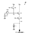
- FIG. 2 is a circuit diagram showing an example of a pixel circuit configuration.
- FIG. 3 is a diagram illustrating a color filter bayer arrangement, three-exposure composition, and a pixel for phase difference detection.
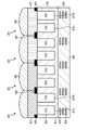
- FIG. 4 is a cross-sectional view showing an example of the cross-sectional structure of the phase difference detection pixel.
- FIG. 5 is an explanatory diagram of measures against blooming.
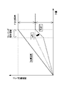
- FIG. 6 is an explanatory diagram for maintaining linearity at the time of pixel addition by taking measures against blooming.
- FIG. 1 is a block diagram schematically showing a system configuration of a CMOS image sensor, which is an example of an image pickup apparatus to which the technique according to the present disclosure is applied.
- FIG. 2 is a circuit diagram showing an example of a pixel circuit configuration.
- FIG. 3 is a
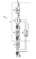
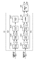
- FIG. 7 is a block diagram schematically showing an example of the configuration of the pixel signal processing unit according to the embodiment of the present disclosure.
- FIG. 8 is a block diagram schematically showing an example of the configuration of the pixel signal processing unit according to the first embodiment.
- FIG. 9 is a diagram schematically showing an example of a three-exposure synthesis process by a blooming determination circuit and a synthesis circuit.
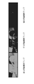
- FIG. 10 is a diagram showing an example of a long-time storage map, a medium-time storage map, and a short-time storage map.
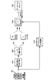
- FIG. 11 is a block diagram schematically showing an example of the configuration of the pixel signal processing unit according to the second embodiment.
- FIG. 12 is a block diagram schematically showing an example of the configuration of the pixel signal processing unit according to the third embodiment.
- FIG. 13 is a block diagram schematically showing an example of the configuration of the pixel signal processing unit according to the fourth embodiment.
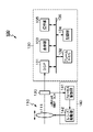
- FIG. 14 is a block diagram schematically showing an outline of the configuration of the imaging system
- Example 4 (Variation example of Example 3: An example in which the pixels for phase difference detection are composed of pixels in an RGB bayer array and the synthesis process is performed outside the sensor). 4. The imaging system of the present disclosure 5. Modification example 6. Configuration that can be taken by this disclosure
- the pixel characteristic correction circuit is configured to perform a process of correcting a sensitivity difference between a pair of photoelectric conversion units as a predetermined correction process.
- the blooming phenomenon is a phenomenon that occurs when one of the photoelectric conversion units of the pair of photoelectric conversion units is saturated first due to the difference in sensitivity of the pair of photoelectric conversion units.
- the blooming determination circuit has a blooming threshold value, and the pixel value of the phase difference detection pixel is blooming. It is possible to determine that the pixel is a phase difference detection pixel in which a blooming phenomenon occurs when the threshold value is equal to or higher than the threshold value. Further, for the synthesis circuit (step), a plurality of pixel signals corresponding to different exposure times are used by using a pair of pixel signals output from the phase difference detection pixels determined by the blooming determination circuit to prevent the blooming phenomenon. It is possible to generate a composite luminance signal by synthesizing the luminance signals.
- the blooming determination circuit (step) is output from the phase difference detection pixel having a pixel value equal to or higher than the blooming threshold value.
- the pair of pixel signals to be generated can be configured to generate a blend map for each exposure time so as not to be used for generating a composite brightness signal.
- the composition circuit (step) can be configured to perform composition processing by adjusting the luminance level according to the exposure ratio.
- the luminance step generated at the switching point of the pixel data of different exposure times is set in the synthesis circuit (step). , It can be configured to be relaxed by the blending process using the blend map. Further, regarding the phase difference detection pixel, when one of the photoelectric conversion units of the pair of photoelectric conversion units is saturated first due to the sensitivity difference of the pair of photoelectric conversion units, the saturated signal is transmitted to the other photoelectric conversion unit. It is possible to have a configuration having a pixel structure that allows the pixel structure to escape.
- the phase difference detection pixels are completely provided as all the pixels of the pixel array unit.
- the phase difference detection pixel may be configured such that the color filter is composed of pixels in a bayer array or is composed of white pixels.
- CMOS Complementary Metal Oxide Semiconductor
- a CMOS image sensor is an image sensor made by applying or partially using a CMOS process.
- FIG. 1 is a block diagram schematically showing a system configuration of a CMOS image sensor, which is an example of an image pickup apparatus to which the technique according to the present disclosure is applied.
- the CMOS image sensor 1 has a configuration including a pixel array unit 11 and a peripheral circuit unit arranged around the pixel array unit 11.
- the pixel array unit 11 has a configuration in which pixels 20 including a photoelectric conversion unit (photoelectric conversion element) are two-dimensionally arranged in a row direction and a column direction, that is, in a matrix.
- the row direction means the arrangement direction of the pixels 20 in the pixel row
- the column direction means the arrangement direction of the pixels 20 in the pixel row.
- the pixel 20 generates and accumulates a light charge corresponding to the amount of received light by performing photoelectric conversion in the photoelectric conversion unit.
- the peripheral circuit unit of the pixel array unit 11 is composed of, for example, a row selection unit 12, a load MOS unit 13, a column signal processing unit 14, an output circuit unit 15, a pixel signal processing unit 16, a timing control unit 17, and the like.
- Peripheral circuit units such as row selection unit 12, load MOS unit 13, column signal processing unit 14, output circuit unit 15, pixel signal processing unit 16, and timing control unit 17 are, for example, the same semiconductor substrate as the pixel array unit 11. It has a structure formed on the 18.
- the semiconductor chip structure a so-called flat-mounted semiconductor chip structure in which a peripheral circuit portion is formed on the same semiconductor substrate (semiconductor chip) as the pixel array portion 11 is exemplified, but the flat-mounted semiconductor chip is illustrated. It is not limited to the structure. That is, at least two semiconductor substrates, a first-layer semiconductor substrate and a second-layer semiconductor substrate, are laminated, a pixel array portion 11 is formed on the first-layer semiconductor substrate, and a peripheral circuit portion is formed on the second-layer semiconductor substrate. Can be formed into a so-called laminated semiconductor chip structure.
- the pixel array portion 11 on the first-layer semiconductor substrate and the peripheral circuit portion on the second-layer semiconductor substrate are Cu-Cu that directly joins the Cu electrodes to each other. It is electrically connected via a direct junction, a junction made of a through silicon via (Through Silicon Via: TSV), microbumps, etc. (not shown).
- pixel control lines 31 (31 1 to 31 m ) are wired along the row direction for each pixel row with respect to the matrix-shaped pixel array. Further, signal lines 32 ( 321 to 32 n ) are wired along the row direction for each pixel row.
- the pixel control line 31 transmits a drive signal for driving when reading a signal from the pixel 20.
- the pixel control line 31 is shown as one wiring, but the wiring is not limited to one.
- One end of the pixel control line 31 is connected to the output end corresponding to each row of the row selection unit 12.
- each component of the peripheral circuit section of the pixel array section 11, that is, the row selection section 12, the load MOS section 13, the column signal processing section 14, the output circuit section 15, the pixel signal processing section 16, and the timing control section is composed of 17 mag.
- the row selection unit 12, the load MOS unit 13, the column signal processing unit 14, the output circuit unit 15, the pixel signal processing unit 16, and the timing control unit 17 will be described.
- the row selection unit 12 is composed of a shift register, an address decoder, and the like, and controls the scanning of the pixel row and the address of the pixel row when selecting each pixel 20 of the pixel array unit 11. Although the specific configuration of the row selection unit 12 is not shown, it generally has two scanning systems, a read scanning system and a sweep scanning system.
- the read scanning system selectively scans the pixels 20 of the pixel array unit 11 row by row in order to read the pixel signal from the pixels 20.
- the pixel signal read from the pixel 20 is an analog signal.
- the sweep scanning system performs sweep scanning in advance of the read scan performed by the read scan system by the time of the shutter speed.
- the photoelectric conversion element is reset by sweeping out unnecessary charges from the photoelectric conversion element of the pixel 20 in the read row. Then, by sweeping out (resetting) unnecessary charges by this sweeping scanning system, a so-called electronic shutter operation is performed.
- the electronic shutter operation refers to an operation of discarding the optical charge of the photoelectric conversion element and starting a new exposure (starting the accumulation of the optical charge).
- the signal read by the read operation by the read scan system corresponds to the amount of light received after the read operation or the electronic shutter operation immediately before that.
- the period from the read timing by the immediately preceding read operation or the sweep timing by the electronic shutter operation to the read timing by the current read operation is the exposure period of the light charge in the pixel 20.
- the load MOS unit 13 is composed of a set of current sources I (see FIG. 2) composed of MOS transistors connected to each of the vertical signal lines 32 ( 321 to 32 n ) for each pixel row, and is selected by the row selection unit 12. A bias current is supplied to each pixel 20 in the scanned pixel row through each of the vertical signal lines 32 ( 321 to 32 n ) .
- the column signal processing unit 14 is composed of a set of circuit units provided corresponding to the pixel strings of the pixel array unit 11, and noise reduction is performed for each pixel column with respect to the pixel signal output from the pixel 20 in pixel row units. Signal processing such as. Specifically, the column signal processing unit 14 performs signal processing such as CDS (Correlated Double Sampling) processing for removing fixed pattern noise peculiar to pixels and analog-to-digital conversion processing. .. The pixel data signal-processed by the column signal processing unit 14 is supplied to the output circuit unit 15 through the output signal line L.
- CDS Correlated Double Sampling
- the output circuit unit 15 reads pixel data from the column signal processing unit 14 through the output signal line L and performs predetermined signal processing. Specifically, the output circuit unit 15 performs predetermined signal processing such as correction of vertical line defects and point defects, or signal clamping, and further, parallel-serial conversion, compression, coding, addition, and averaging. , And digital signal processing such as intermittent operation is performed and output as image data.
- predetermined signal processing such as correction of vertical line defects and point defects, or signal clamping, and further, parallel-serial conversion, compression, coding, addition, and averaging.
- digital signal processing such as intermittent operation is performed and output as image data.
- the pixel signal processing unit 16 is a circuit portion to which the technique of the present disclosure is applied, and details such as its configuration and operation will be described later.
- the timing control unit 17 generates various timing signals, clock signals, control signals, etc. based on the synchronization signal given from the outside. Then, the timing control unit 17 performs drive control of the row selection unit 12, the column signal processing unit 14, the pixel signal processing unit 16, and the like based on these generated signals.
- FIG. 2 is a circuit diagram showing an example of the circuit configuration of the pixel 20.
- the pixel 20 has, for example, a photodiode 21 as a photoelectric conversion element.
- the pixel 20 has a transfer transistor 22, a reset transistor 23, an amplification transistor 24, and a selection transistor 25.
- the four transistors of the transfer transistor 22, the reset transistor 23, the amplification transistor 24, and the selection transistor 25, for example, an N-channel MOS type field effect transistor is used.
- the combination of the conductive type of the four transistors 22 to 25 exemplified here is only an example, and is not limited to these combinations.
- a plurality of pixel control lines are commonly wired to each pixel 20 in the same pixel row as the pixel control lines 31 (31 1 to 31 m ) described above for the pixel 20. These plurality of pixel control lines are connected to the output end corresponding to each pixel row of the row selection unit 12 in pixel row units.
- the row selection unit 12 appropriately outputs the transfer signal TRG, the reset signal RST, and the selection signal SEL to the plurality of pixel control lines.
- the anode electrode is connected to a low-potential side power supply (for example, ground), and the received light is photoelectrically converted into a light charge (here, photoelectrons) having a charge amount corresponding to the light amount, and the light thereof is converted. Accumulates electric charge.
- the cathode electrode of the photodiode 21 is electrically connected to the gate electrode of the amplification transistor 24 via the transfer transistor 22.
- the region in which the gate electrode of the amplification transistor 24 is electrically connected is a floating diffusion (floating diffusion region / impurity diffusion region) FD.
- the floating diffusion FD is a charge-voltage conversion unit that converts electric charge into voltage.
- a transfer signal TRG in which a high level (for example, V DD level) is active is given to the gate electrode of the transfer transistor 22 from the row selection unit 12.
- the transfer transistor 22 becomes conductive in response to the transfer signal TRG, is photoelectrically converted by the photodiode 21, and transfers the optical charge stored in the photodiode 21 to the floating diffusion FD.
- the reset transistor 23 is connected between the node of the high potential side power supply voltage V DD and the floating diffusion FD.
- a reset signal RST that activates a high level is given to the gate electrode of the reset transistor 23 from the row selection unit 12.
- the reset transistor 23 becomes conductive in response to the reset signal RST, and resets the floating diffusion FD by discarding the charge of the floating diffusion FD to the node of the voltage V DD .
- the gate electrode is connected to the floating diffusion FD, and the drain electrode is connected to the node of the high potential side power supply voltage VDD .
- the amplification transistor 24 serves as an input unit for a source follower that reads out a signal obtained by photoelectric conversion in the photodiode 21. That is, in the amplification transistor 24, the source electrode is connected to the signal line 32 via the selection transistor 25.
- the drain electrode is connected to the source electrode of the amplification transistor 24, and the source electrode is connected to the signal line 32.
- a selection signal SEL in which a high level is active is given to the gate electrode of the selection transistor 25 from the row selection unit 12.
- the selection transistor 25 enters a conduction state in response to the selection signal SEL, so that the signal output from the amplification transistor 24 is transmitted to the signal line 32 with the pixel 20 in the selection state.
- the pixel 20 is composed of a transfer transistor 22, a reset transistor 23, an amplification transistor 24, and a selection transistor 25, that is, a 4Tr configuration composed of four transistors (Tr) is given as an example.
- the selection transistor 25 may be omitted, and the amplification transistor 24 may have a 3Tr configuration in which the function of the selection transistor 25 is provided. If necessary, the number of transistors may be increased to a configuration of 5Tr or more. ..
- a reset signal (so-called P-phase signal) which is a reset level at the time of resetting the floating diffusion FD by the reset transistor 23, and a signal level based on photoelectric conversion in the photodiode 21.
- Data signals (so-called D-phase signals) are output in order. That is, the pixel signal output from the pixel 20 includes a reset signal at the time of reset and a data signal at the time of photoelectric conversion by the photodiode 21.
- each pixel 20 of the pixel array unit 11 has, for example, a color filter 47 (see FIG. 4) in units of 4 pixels of 2 ⁇ 2 (2 pixels in the column direction ⁇ 2 pixels in the row direction). ) Is placed.
- the color filter 47 may not be arranged.
- the bayer arrangement of R (red) G (green) B (blue) shown in FIG. 3 is illustrated.
- the arrangement example of the color filter is not limited to the bayer arrangement and the RGB primary color filter, and various configurations such as a complementary color filter such as C (cyan) M (magenta) Y (yellow) are applied. May be done.
- the CMOS image sensor 1 having the above configuration is configured to acquire a plurality of pixel signals having different exposure times in order to achieve a wide dynamic range, that is, to generate an image having a wide dynamic range. ..
- a pixel signal with a relatively long exposure time and a long-time storage a pixel signal with a relatively medium exposure time and a medium-time storage
- a short-time storage with a relatively short exposure time 3 An example is illustrated in which a wide dynamic range is achieved by synthesizing pixel signals based on different types of exposure times (hereinafter, abbreviated as "3 exposures").
- the long-time storage pixel is L
- the medium-time storage pixel is M
- the short-time storage pixel S is shown.
- Pixel L, medium-time storage pixel M, and short-time storage pixel S are arranged.
- the phase difference is partially or wholly detected in the two-dimensional arrangement of the pixels 20. It has a configuration in which pixels are arranged.
- a configuration in which all the pixels 20 in the pixel array unit 11 are phase difference detection pixels that is, a configuration in which the phase difference detection pixels 20 are completely arranged in the pixel array unit 11 is illustrated.
- the phase difference detection pixel 20 has a pair of photoelectric conversion units, that is, a pair of left and right photodiodes 21L divided into left and right (L / R) in the row direction of the two-dimensional arrangement of the pixels 20. , 21R.
- the pair of photodiodes 21L and 21R have different formation positions in one pixel 20.
- the images generated from the signals of the pair of L / R photodiodes 21L and 21R are displaced. Therefore, by detecting the relative position of each L / R image based on the respective signals of the pair of photodiodes 21L and 21R, it is possible to detect the defocus amount and the defocus direction used in the autofocus described later.
- phase difference detection pixel a pixel having a pair of photodiodes 21L and 21R and capable of detecting a defocus amount and a defocus direction used in autofocus is referred to as a phase difference detection pixel. ..
- the phase difference detection pixel is not only used for detecting the defocus amount and the defocus direction, but is also used by adding the signals of the pair of photodiodes 21L and 21R in the same manner as the normal pixel. It can also be used as a pixel for acquiring a pixel signal of one pixel, and can be used for calculating depth information (Depth) from the difference information of a pair of L / R synthetic brightness data.
- the color filter arrangement is, for example, an RGB bayer arrangement, and the exposure times are different for long-time storage, medium-time storage, and
- the pixel array unit 11 has, for example, the entire phase difference detecting pixel 20 capable of detecting the defocus amount and the defocus direction.
- the photodiodes 21L and 21R are formed by forming the N-type (second conductive type) semiconductor region 42 in the P-type (first conductive type) semiconductor region 31.
- a pair of left and right photodiodes 21L and 21R are formed in one pixel of the phase difference detection pixel 20.
- the pair of left and right photodiodes 21L and 21R are formed so that the pixel region is evenly divided into two and arranged symmetrically.
- a pixel transistor (not shown) that is generated by a pair of left and right photodiodes 21L and 21R of the phase difference detection pixel 20 and reads out the accumulated charge and the like (not shown).
- a plurality of wirings 43, and a multilayer wiring layer 45 composed of an interlayer insulating film 44 are formed.
- an inter-pixel light-shielding film 46 is formed at the pixel boundary portion on the back surface side of the semiconductor substrate 18 on the upper side in FIG.
- the inter-pixel light-shielding film 46 may be any material that blocks light, but a material that has strong light-shielding properties and can be processed with high precision by microfabrication, for example, etching is desirable.
- the interpixel light-shielding film 46 can be formed of, for example, a metal film such as tungsten (W), aluminum (Al), copper (Cu), titanium (Ti), molybdenum (Mo), and nickel (Ni).
- an antireflection film made of a silicon oxide film or the like may be further formed on the back surface side interface of the semiconductor substrate 18.
- a color filter 47 is formed on the back surface of the semiconductor substrate 18 including the interpixel light-shielding film 46.
- the color filter 47 is formed by rotationally applying a photosensitive resin containing a dye such as a pigment or a dye.
- a photosensitive resin containing a dye such as a pigment or a dye.
- an on-chip lens 48 is formed in pixel units, that is, in common with a pair of photodiodes 21L and 21R.
- the on-chip lens 48 is formed of, for example, a resin-based material such as a styrene-based resin, an acrylic resin, a styrene-acrylic copolymer resin, or a siloxane-based resin.
- the image pickup apparatus to which the technique of the present disclosure is applied has a color filter 47 or an on-chip on the back surface side opposite to the front surface side of the semiconductor substrate 18 on which the multilayer wiring layer 45 is formed. It is a back-illuminated CMOS image sensor 1 that forms a lens 48 and captures light emitted from the back surface side.
- the type is not limited to the backside irradiation type, and a surface irradiation type that captures the light emitted from the front side can also be used.
- the CMOS image sensor 1 is provided with a phase difference detection pixel 20 having a pair of left and right (L / R) photodiodes 21L and 21R while being able to acquire a plurality of pixel signals having different exposure times.
- the signals of the pair of photodiodes 21L and 21R can be used for the calculation of depth information (Dept).
- predetermined signal processing is performed on a plurality of pixel signals L / R having different exposure times, which are output from a pair of photodiodes 21L and 21R for each pixel.
- a predetermined pixel signal L / R for long-time storage, medium-time storage, and short-time storage output from the pair of photodiodes 21L and 21R is used.
- a sensitivity difference may occur between the pair of photodiodes 21L and 21R.
- a blooming phenomenon in which the linearity of the pixel data of one pixel after adding the signals of the pair of photodiodes 21L and 21R cannot be maintained occurs. Occur. If the linearity of the pixel data cannot be maintained due to the occurrence of the blooming phenomenon, a luminance step occurs at the switching points of the pixel data having different exposure times, and erroneous depth information is detected at the step portion.
- the phase difference detection pixel 20 has the following pixel structure.
- An explanatory diagram of this blooming countermeasure is shown in FIG.
- the upper view of FIG. 5 is an enlarged plan view of the phase difference detection pixel 20 of the medium-time storage (M) of the 2 ⁇ 2 pixels of R, and the lower view of FIG. 5 is a pair of photos.
- It is a potential conceptual diagram which shows the potential of a diode 21L, 21R schematically.
- the phase difference detection pixel 20 has a pixel structure in which the potential barrier 201 between the pair of L / R photodiodes 21L and 21R is formed lower than the potential barrier 202 at the pixel boundary.
- the impurity concentration of the impurity layer between the pair of photodiodes 21L and 21R (not shown in FIG. 4) that separates the pair of photodiodes 21L and 21R is adjusted. By doing so, it can be formed to be lower than the potential barrier 202 at the pixel boundary.
- the sensitivity difference between the pair of photodiodes 21L and 21R causes the sensitivity difference.
- one of the pair of photodiodes 21L and 21R (photodiode 21L in the example of FIG. 5) is saturated first, the saturated signal can be released to the other (photodiode 21R in the example of FIG. 5).
- FIG. 6 shows an explanatory diagram of maintaining linearity at the time of pixel addition by the above-mentioned blooming countermeasure. Since the image data (for example, the bayer array) output to the outside of the sensor is used by adding the signals of the pair of L / R photodiodes 21L and 21R, the problem of blooming phenomenon is not affected by the above blooming countermeasures. ..
- CMOS image sensor 1 using the phase difference detection pixel 20 a pair of L / R photodiodes for detecting defocus information (defocus amount and defocus direction) for autofocus or depth information. Signal processing is performed with the 21L and 21R signals separated. Therefore, when the blooming phenomenon occurs, the linearity of the pixel data cannot be maintained, and the signal levels at the time of synthesis do not match.
- FIG. 7 schematically shows a block diagram of an example of the configuration of the pixel signal processing unit according to the embodiment of the present disclosure, that is, the pixel signal processing unit 16 shown in FIG.
- the pixel signal processing unit 16 can acquire a plurality of pixel signals having different exposure times, and has an L / R pair of photodiodes 21L.
- a predetermined value is provided for a plurality of pixel signals L / R having different exposure times, which are output from a pair of photodiodes 21L, 21R for each pixel.
- It is a signal processing unit for performing signal processing.
- the pixel signal processing unit 16 according to the present embodiment has a configuration including a pixel characteristic correction circuit 161, a luminance signal generation circuit 162, a blooming determination circuit 163, and a synthesis circuit 164.
- the pixel characteristic correction circuit 161 is output from a pair of L / R photodiodes 21L, 21R, and has a plurality of pixel signals L / R having different exposure times, for example, long-time storage, medium-time storage, and short-time storage.
- a predetermined correction process is performed on the three pixel signals L / R.
- the pixel characteristic correction circuit 161 changes the balance of L / R depending on the image height position, as an example of predetermined correction processing, there are 3 types of long-time storage, medium-time storage, and short-time storage. Processing is performed to correct the sensitivity difference between the pair of L / R photodiodes 21L and 21R for one pixel signal L / R.
- the brightness signal generation circuit 162 has different exposure times (long-time storage) based on three pixel signals L / R of long-time storage, medium-time storage, and short-time storage after correction processing by the pixel characteristic correction circuit 161. , Medium-time storage, and short-time storage) to generate a plurality of brightness signals (brightness data) L / R.
- the blooming determination circuit 163 detects the phase difference based on the pixel signal before the correction process in the pixel characteristic correction circuit 161, that is, the three pixel signals L / R of long-time storage, medium-time storage, and short-time storage. It is determined whether or not the blooming phenomenon has occurred in the pixel 20.
- the pixel value at which linearity cannot be maintained due to the influence of the occurrence of the blooming phenomenon depends on the characteristics of the phase difference detection pixel 20. Therefore, a blooming threshold value is set in the blooming determination circuit 163. Then, the blooming determination circuit 163 determines that the phase difference detection pixel 20 has a blooming phenomenon when the pixel value before the correction process in the pixel characteristic correction circuit 161 is equal to or greater than the blooming threshold value.
- the synthesis circuit 164 has a plurality of luminance signals corresponding to different exposure times based on the determination result of the blooming determination circuit 163, that is, three luminance data L / R of long-term storage, medium-time storage, and short-time storage. Is combined and output as the combined luminance data L / R. Specifically, the synthesis circuit 164 excludes the phase difference detection pixel 20 determined by the blooming determination circuit 163 that the blooming phenomenon has occurred, and the phase difference detection pixel 20 determined that the blooming phenomenon has not occurred. For 20, the three luminance data L / R of long-term storage, medium-time storage, and short-time storage are combined and output as the combined luminance data L / R.
- the reason why the pixel in which the blooming phenomenon is generated is determined based on the data before the correction processing in the pixel characteristic correction circuit 161 is as follows. That is, the signal level of the L / R changes due to the correction processing such as the sensitivity difference in the pixel characteristic correction circuit 161 and the signal level of the original pixel cannot be known. Further, since the luminance data after the sensor output is subjected to various signal processing, the original signal level cannot be restored for the same reason. Therefore, by performing the blooming determination process and the synthesis process using the blooming determination process based on the data before the correction process in the pixel characteristic correction circuit 161, it is possible to accurately determine the linearity maintenance.
- the contrast is an important point when calculating the depth data from the difference information of the L / R pair of synthetic luminance data.
- sufficient contrast cannot be obtained with luminance data stored only for medium time, and it is easy to calculate erroneous depth data. Therefore, more accurate depth data can be calculated by using the combined luminance data L / R having a wide dynamic range.
- the pixel data of one pixel can be acquired.
- the pixel characteristic correction circuit 161 the brightness signal generation circuit 162, the blooming determination circuit 163, and the synthesis are performed.
- the circuit 164 is replaced with a pixel characteristic correction step, a brightness signal generation step, a blooming determination step, and a synthesis step.
- the pixel signal processing unit uses the pixel data before the sensitivity correction processing by the pixel characteristic correction circuit 161 for phase difference detection in which the blooming phenomenon occurs.
- the pixel 20 is determined, and the pixel data of the phase difference detection pixel 20 in which the blooming phenomenon does not occur is used to perform the synthesis processing of the three exposure brightness data.
- the combined luminance data L / R having a wider dynamic range can be obtained as compared with the case of using one luminance data, so that the detection accuracy of the depth information in the dark part or the bright part can be improved.
- the luminance step does not occur at the switching point of the pixel data having different exposure times, the detection of erroneous depth information does not occur.
- the first embodiment is an example in which the functions of avoiding the influence of blooming and synthesizing three exposure luminance data are incorporated in the luminance data generation block.
- FIG. 8 schematically shows a block diagram of an example of the configuration of the pixel signal processing unit according to the first embodiment.
- the brightness data generation block 50 has a gradation compression circuit 165 in addition to the brightness signal generation circuit 162, the blooming determination circuit 163, and the synthesis circuit 164, and is a pair of L / R photodiodes of the phase difference detection pixels 20.
- a composite brightness signal L based on a plurality of pixel signals L / R with different exposure times output from 21L and 21R, for example, three pixel signals L / R of long-term storage, medium-time storage, and short-time storage. Generate / R.
- the luminance data generation block 50 has a function of avoiding the influence of blooming based on the determination result of the blooming determination circuit 163 and a function of synthesizing three exposure luminance data by the luminance signal generation circuit 162 and the synthesis circuit 164.
- the blooming determination circuit 163 blooms based on the pixel data before the sensitivity difference correction process in the pixel characteristic correction circuit 161, that is, the three pixel data L / R of long-time storage, medium-time storage, and short-time storage. Detect the pixel where the phenomenon is occurring. Since the R / G / G / B pixel data of the Bayer array is used to generate the luminance data in the luminance signal generation circuit 162, if the blooming phenomenon occurs in any one of the pixels, the pixel data is used. Luminance data cannot be used. Further, since it affects the L / R of the same color pixel in which the blooming phenomenon occurs, both the L / R of the generated luminance data cannot be used.
- the blooming determination circuit 163 creates a blend map as a blooming determination result for each of the pixel data of long-time storage, medium-time storage, and short-time storage based on the information of the pixel in which the blooming phenomenon occurs.
- the blend map of the pixel data accumulated for a long time is used in combination with the luminance data accumulated for a long time, and is used to extract only usable pixels, that is, pixels in which the blooming phenomenon does not occur.
- FIG. 9 is a diagram schematically showing an example of a three-exposure composition process by the blooming determination circuit 163 and the composition circuit 164.
- Three types of luminance data L / R for long-term storage, medium-time storage, and short-time storage by the luminance signal generation circuit 162, and a blend map by the blooming determination circuit 163 are generated.
- the luminance data of each of the long-time, medium-time, and short-time exposure times of 10 bits is multiplied by the blend map, and the luminance data synthesized by 3 exposures is generated in each of L / R.
- the combined luminance data L / R after the three-exposure composition processing is expanded to 16 bits, but is compressed to 10 bits by the gamma processing and the limit processing in the gradation compression circuit 165 in the subsequent stage.
- the contrast tends to be weak in the low illuminance region, so that the gradation compression circuit 165 performs gamma processing.
- This gamma processing is not indispensable, and it is possible to perform processing not only inside the CMOS image sensor but also outside the CMOS image sensor.
- the luminance signal generation circuit 162 includes each functional unit of the L / R separation unit 1621, the channel decomposition unit 1622, and the luminance signal generation unit 1623.
- the L / R separation unit 1621 performs L / R separation on the pixel data after the sensitivity difference correction.
- the channel decomposition unit 1622 performs channel decomposition for dividing L / R pixel data in units of 2 ⁇ 2 4 pixels into the same group for each exposure time.
- the luminance signal generation unit 1623 generates the luminance data of L ⁇ 4 and the luminance data of R ⁇ 4 based on the pixel data of L ⁇ 4 and the pixel data of R ⁇ 4 channel-decomposed by the channel decomposition unit 1622. It is supplied to the synthesis circuit 164.
- the blooming determination circuit 163 includes each functional unit of the L / R separation unit 1631, the channel decomposition unit 1632, the blooming determination unit 1633, and the blend map generation unit 1634.
- the L / R separation unit 1631 performs L / R separation on the pixel data before the sensitivity difference correction.
- the channel decomposition unit 1632 performs channel decomposition for dividing L / R pixel data in units of 2 ⁇ 2 4 pixels into the same group for each exposure time.
- the blooming determination unit 1633 determines whether or not a blooming phenomenon has occurred in the phase difference detection pixel 20 based on the L ⁇ 4 pixel data and the R ⁇ 4 pixel data channel-decomposed by the channel decomposition unit 1622. conduct. Since the pixel value at which linearity cannot be maintained due to the influence of the occurrence of the blooming phenomenon depends on the pixel characteristics, the pixel at which the blooming phenomenon occurs is determined using the threshold parameter. Specifically, the blooming determination unit 1633 determines that a pixel whose pixel value is equal to or greater than the blooming threshold value is a pixel in which the blooming phenomenon has occurred.
- the blend map generation unit 1634 creates a blend map for each of the pixel data of long-term storage, medium-time storage, and short-time storage based on the information of the pixels determined by the blooming determination unit 1633 that the blooming phenomenon has occurred. create. Specifically, the blend map generation unit 1634 generates a map for each exposure time so that the pixel value is not used for the pixel whose pixel value is equal to or larger than the blooming threshold, that is, the pixel in which the blooming phenomenon occurs.
- FIG. 10 shows an example of a long-time storage map, a medium-time storage map, and a short-time storage map.
- the blend map generation unit 1634 performs a simple blend process, expands the number of bits of the map so as to blend pixel data having different exposure times from the stage before the pixel value exceeds the blooming threshold, and generates a blend map. It is composed.
- the synthesis circuit 164 uses the blend map generated by the blend map generation unit 1634 of the blooming determination circuit 163, and accumulates for a long time by blending the luminance data of long-term storage, medium-time storage, and short-time storage. , Medium-time storage, and short-time storage of three exposure luminance data are combined. Specifically, in order to match the overall luminance level based on the luminance data accumulated for a long time, the luminance data obtained by multiplying the luminance data accumulated for medium time by the exposure ratio and the luminance data accumulated for a short time are used as the exposure ratio 2. Prepare the multiplied brightness data in advance.
- the synthesis circuit 164 generates 3-exposure composite luminance data by multiplying and adding the above-mentioned blend map and the luminance data prepared in advance.
- the pixel signal processing unit 16 adjusts the brightness for each local area and performs a process of blending.
- the composition processing is performed by simply switching the luminance data whose exposure ratio is doubled, in other words, by adjusting the luminance level according to the exposure ratio. To reduce the weight of the processing.
- the boundary of a plurality of luminance data having different exposure times is switched by the blend processing by the blend map to suppress a sudden change in the signal level and the luminance step. Is relaxing.
- the second embodiment is an example in which the phase difference detection pixel is composed of a white pixel without a color filter.
- FIG. 11 schematically shows a block diagram of an example of the configuration of the pixel signal processing unit according to the second embodiment.
- the phase difference detection pixels 20 are composed of white pixels without a color filter and are white. It is configured to perform a plurality of exposure composition processing using only pixels, for example, a three-exposure composition process of long-term storage, medium-time storage, and short-time storage. That is, if the pixel structure has a pair of photodiodes 21L and 21R and is capable of outputting a plurality of pixel signals having different exposure times, the composition processing is the same as in the case of the first embodiment, not limited to the RGB bayer arrangement. It is possible to do.
- the pixel characteristic correction circuit 161 is output from a pair of L / R photodiodes 21L, 21R, and has a plurality of pixel data L / Rs having different exposure times, for example, long-time storage, medium-time storage, and short-time storage.
- a predetermined correction process is performed on the three pixel data L / R.
- the pixel characteristic correction circuit 161 changes the balance of L / R depending on the image height position, as an example of predetermined correction processing, there are 3 types of long-time storage, medium-time storage, and short-time storage. Processing is performed to correct the sensitivity difference between the pair of L / R photodiodes 21L and 21R for one pixel data L / R.
- the L / R separation circuit 166 stores three pixel data L / R, which are accumulated for a long time, medium time, and short time after the correction process in the pixel characteristic correction circuit 161 for a long time and medium time. Pixel data accumulated and stored for a short time and pixel data accumulated for a long time, medium time, and short time of R are separated and supplied to the synthesis circuit 164. In the case of the phase difference detection pixel 20 composed of white pixels, the pixel data is luminance data.
- the synthesis circuit 164 Based on the determination result of the blooming determination circuit 163, the synthesis circuit 164 synthesizes three luminance data L / R of long-time storage, medium-time storage, and short-time storage, and obtains three exposure composite luminance data L / R. Output. Specifically, the synthesis circuit 164 has three types of phase difference detection pixels 20 determined by the blooming determination circuit 163 that the blooming phenomenon has not occurred: long-time storage, medium-time storage, and short-time storage. The brightness data L / R is combined. The three-exposure composite luminance data L / R output from the composite circuit 164 is supplied to, for example, an application processor 60 provided outside the sensor.
- the phase difference detection pixel 20 is composed of white pixels, and the three-exposure composition process is performed using only the white pixels.
- white pixels it is not necessary to generate luminance (Y) data. Therefore, by synthesizing using the pixel data of long-term storage, medium-time storage, and short-time storage as they are. It is possible to output L / R three-exposure composite luminance data.
- the third embodiment is an example in which the phase difference detection pixel is composed of a white pixel without a color filter, and the synthesis process is performed outside the sensor.
- FIG. 12 schematically shows a block diagram of an example of the configuration of the pixel signal processing unit according to the third embodiment.
- the pixel signal processing unit 16 is configured to generate the three-exposure composite luminance data L / R by using the application processor 60 provided outside the sensor.
- the application processor 60 outside the sensor from the L / R separation circuit 166 inside the sensor, pixel data of long-term storage, medium-time storage, and short-time storage of L, and long-term storage and medium-time storage of R, In addition, pixel data stored for a short time is supplied.
- the application processor 60 performs the blooming determination process in the same manner as the blooming determination circuit 163 of the first embodiment by software processing, and also performs the three-exposure composition process in the same manner as the synthesis circuit 164 of the first embodiment. 3 Output the combined exposure brightness data L / R.
- the load on the application processor 60 becomes heavy because the blooming determination processing and the three-exposure composition processing are performed outside the sensor. Therefore, from the viewpoint of reducing the load on the application processor 60, it can be said that it is preferable to perform the blooming determination process and the three-exposure composition process in the sensor as in the case of the first and second embodiments. ..
- the fourth embodiment is a modification of the third embodiment, in which the pixels for phase difference detection are composed of pixels in an RGB bayer array, and the synthesis process is performed outside the sensor.
- FIG. 13 schematically shows a block diagram of an example of the configuration of the pixel signal processing unit according to the fourth embodiment.
- the application processor 60 performs luminance data generation processing in the same manner as the luminance signal generation circuit 162 of the first embodiment, and performs luminance determination processing in the same manner as the blooming determination circuit 163 of the first embodiment by software processing.
- the 3-exposure composition processing is output.
- the load of the application processor 60 is higher than that in the case of the third embodiment in order to perform the luminance data generation processing, the blooming determination processing, and the three-exposure composition processing outside the sensor. It will be even heavier. Therefore, from the viewpoint of reducing the load on the application processor 60, it can be said that it is preferable to perform the blooming determination process and the three-exposure composition process in the sensor as in the case of the first and second embodiments. ..
- FIG. 14 is a block diagram schematically showing an outline of the configuration of the imaging system of the present disclosure.
- the image pickup system 100 of the present disclosure includes an optical system 110, an image pickup element 120, a signal processing unit 130, and an autofocus unit 140.
- the optical system 110 is composed of an image pickup lens 111, a diaphragm (not shown), and the like.
- the image pickup lens 111 is shown as one lens, but the present invention is not limited to this. That is, the image pickup lens 111 may be composed of one lens or may be composed of a plurality of lenses.
- the image pickup element 120 converts the amount of incident light beam imaged on the image pickup surface by the image pickup lens 111 into an electric signal in pixel units and outputs it as a pixel signal.
- the image pickup element 120 includes a CMOS image sensor according to the above-described embodiment, that is, a pixel array unit including a phase difference detection pixel having a pair of photoelectric conversion units in a two-dimensional arrangement of pixels, and is used for phase difference detection.
- a CMOS image sensor capable of outputting a plurality of pixel signals having different exposure times can be used from each pixel of the pixel array unit including the pixels. From this CMOS image sensor, for example, three-exposure composite luminance data L / R is output to the autofocus unit 140.
- the signal processing unit 130 has a configuration including a DSP (Digital Signal Processor) circuit 131, a frame memory 132, a display unit 133, a recording unit 134, an operation system 135, and the like.
- the DSP circuit 131, the frame memory 132, the display unit 133, the recording unit 134, and the operation system 135 are connected to each other via the bus line 136 so as to be communicable with each other.
- the DSP circuit 131 performs various well-known signal processing on the image pickup signal supplied from the image pickup element 120 while using the frame memory 132 as necessary.
- the display unit 133 comprises a panel-type display device such as a liquid crystal display device or an organic EL (electroluminescence) display device, and displays a moving image or a still image captured by the image pickup device 120.
- the recording unit 134 records a moving image or a still image captured by the image sensor 120 on a recording medium such as a hard disk or a DVD.
- the operation system 135 issues operation commands for various functions of the image pickup system 100 under the operation of the photographer.
- the signal processing unit 130 is also provided with a power supply system, which operates the DSP circuit 131, the frame memory 132, the display unit 133, the recording unit 134, and the operation system 135.
- Various power sources that serve as power sources are appropriately supplied to these supply targets.
- the autofocus unit 140 has a configuration including a focus control unit 141, a lens drive unit 142, and the like.
- the three-exposure composite luminance data L / R generated by the image sensor 120 is supplied to the lens driving unit 142.
- the focus control unit 141 is configured by a microcomputer or the like, and based on the three-exposure composite brightness data L / R supplied from the image pickup element 120, the focus shift amount and shift direction of the image pickup lens 111, that is, the defocus amount and Generates a phase difference detection signal that indicates the defocus direction. Then, the focus control unit 141 moves the image pickup lens 111 in the optical axis direction via the lens drive unit 142 based on the generated phase difference detection signal to bring the image pickup lens 111 into a focused state. I do.
- the image pickup system 100 of the present disclosure uses the CMOS image sensor according to the above-described embodiment as the image pickup element 120, and the CMOS image sensor has different exposure times due to the occurrence of the blooming phenomenon. It is possible to avoid the occurrence of a luminance step at the switching point of the pixel data of. Therefore, since the CMOS image sensor outputs the multi-exposure composite luminance data L / R without the occurrence of the luminance step at the switching points of the pixel data with different exposure times, it is based on the multi-exposure composite luminance data L / R. Autofocus control can be performed more accurately.
- the image pickup system 100 of the present disclosure can be used as an image pickup unit of various electronic devices including a mobile terminal device having an image pickup function such as a smartphone.
- the technique according to the present disclosure has been described above based on the preferred embodiment, the technique according to the present disclosure is not limited to the embodiment.
- the configuration and structure of the image pickup apparatus described in the above embodiment are examples, and can be changed as appropriate.
- the configuration of three exposures of long-term storage, medium-time storage, and short-time storage has been described as an example, but the configuration is not limited to the three-exposure configuration, and the configuration is two-exposure.
- the configuration may be 4 or more exposures.
- the luminance data to be combined and output can be realized only with the G pixel data, although the accuracy is reduced.
- the circuit scale can be made smaller than the case where the composite luminance data is output using the data of each pixel of RGB, it can be said that the configuration is advantageous when the chip size is prioritized.
- the present disclosure may also have the following configuration.
- Imaging device ⁇ [A-01] Pixels are arranged two-dimensionally in a matrix, and a pixel array unit including a phase difference detection pixel having a pair of photoelectric conversion units in the two-dimensional arrangement of the pixels, and a pixel array unit. It is equipped with a pixel signal processing unit that processes the pixel signal output from the phase difference detection pixel. It is possible to output a plurality of pixel signals having different exposure times from each pixel of the pixel array portion including the pixel for phase difference detection.
- the pixel signal processing unit A pixel characteristic correction circuit that performs predetermined correction processing on a pair of pixel signals output from a pair of photoelectric conversion units.
- a luminance signal generation circuit that generates a plurality of luminance signals corresponding to different exposure times based on a pair of pixel signals after correction processing by the pixel characteristic correction circuit.
- a blooming determination circuit that determines whether or not a blooming phenomenon has occurred in a pixel for phase difference detection based on a pair of pixel signals before correction processing in the pixel characteristic correction circuit, and a blooming determination circuit. It has a composite circuit that generates a composite luminance signal by synthesizing a plurality of luminance signals corresponding to different exposure times based on the determination result of the blooming determination circuit.
- Imaging device [A-02]
- the pixel characteristic correction circuit performs a process of correcting a sensitivity difference between a pair of photoelectric conversion units as a predetermined correction process.
- the image pickup apparatus according to the above [A-01].
- A-03 The blooming phenomenon occurs when one of the photoelectric conversion units of the pair of photoelectric conversion units is saturated first due to the sensitivity difference between the pair of photoelectric conversion units.
- the image pickup apparatus according to the above [A-02].
- the blooming determination circuit has a blooming threshold value, and determines that the phase difference detection pixel has a blooming phenomenon when the pixel value of the phase difference detection pixel is equal to or greater than the blooming threshold value.
- the image pickup apparatus according to the above [A-03].
- the synthesis circuit uses a pair of pixel signals output from the phase difference detection pixels determined by the blooming determination circuit to prevent the blooming phenomenon, and has a plurality of luminances corresponding to different exposure times. Generate a composite luminance signal by synthesizing the signal, The image pickup apparatus according to the above [A-04].
- the blooming determination circuit creates a blend map for each exposure time so as not to be used for generating a composite luminance signal for a pair of pixel signals output from pixels for detecting a phase difference of pixel values equal to or higher than the blooming threshold. Generate, The image pickup apparatus according to the above [A-05].
- the compositing circuit performs compositing processing by adjusting the luminance level according to the exposure ratio.
- the synthesis circuit alleviates the luminance step that occurs at the switching points of pixel data with different exposure times by blending processing using a blend map.
- [A-09] In the phase difference detection pixel, when one of the photoelectric conversion units of the pair of photoelectric conversion units is saturated first due to the sensitivity difference of the pair of photoelectric conversion units, the saturated signal is transmitted to the other. It has a pixel structure that allows it to escape to the photoelectric conversion unit.
- phase difference detection pixels are provided entirely as all the pixels of the pixel array unit.
- the image pickup apparatus according to any one of the above [A-01] to the above [A-09].
- the color filter is composed of pixels in a bayer array.
- the image pickup apparatus according to any one of the above [A-01] to the above [A-09].
- the phase difference detection pixel is composed of white pixels.
- the image pickup apparatus according to any one of the above [A-01] to the above [A-10].
- Pixel signal processing method of image pickup device ⁇ [B-01] Pixels are arranged two-dimensionally in a matrix, and a pixel array unit including a phase difference detection pixel having a pair of photoelectric conversion units is provided in the two-dimensional arrangement of the pixels. It is possible to output a plurality of pixel signals having different exposure times from each pixel of the pixel array portion including the pixel for phase difference detection.
- Pixel characteristic correction step which performs predetermined correction processing on a pair of pixel signals output from a pair of photoelectric conversion units.
- Luminance signal generation step which generates a plurality of luminance signals corresponding to different exposure times based on a pair of pixel signals after correction processing in the pixel characteristic correction step.
- a blooming determination step for determining whether or not a blooming phenomenon has occurred in the phase difference detection pixel based on the pair of pixel signals before the correction process in the pixel characteristic correction step, and It has a synthesis step of generating a composite luminance signal by synthesizing a plurality of luminance signals corresponding to different exposure times based on the determination result of the blooming determination step.
- Pixel signal processing method of an image pickup device [B-02]
- the pixel characteristic correction step as a predetermined correction process, a process of correcting the sensitivity difference between the pair of photoelectric conversion units is performed.
- the pixel signal processing method of the image pickup apparatus according to the above [B-01].
- B-03 The blooming phenomenon occurs when one of the photoelectric conversion units of the pair of photoelectric conversion units is saturated first due to the sensitivity difference between the pair of photoelectric conversion units.
- the pixel signal processing method of the image pickup apparatus according to the above [B-02].
- B-04 In the blooming determination step, it is determined that the pixel has a blooming threshold value and the phase difference detection pixel has a blooming phenomenon when the pixel value of the phase difference detection pixel is equal to or greater than the blooming threshold value.
- the pixel signal processing method of the image pickup apparatus according to the above [B-03].
- [B-05] In the synthesis step, a plurality of luminances corresponding to different exposure times are used by using a pair of pixel signals output from the phase difference detection pixels determined by the blooming determination circuit to prevent the blooming phenomenon. Generate a composite luminance signal by synthesizing the signal, The pixel signal processing method of the image pickup apparatus according to the above [B-04].
- [B-06] In the blooming determination step, for a pair of pixel signals output from pixels for detecting a phase difference of pixel values equal to or higher than the blooming threshold, a blend map is created for each exposure time so as not to be used for generating a composite luminance signal. Generate, The pixel signal processing method of the image pickup apparatus according to the above [B-05].
- the compositing process is performed by adjusting the luminance level according to the exposure ratio.
- the luminance step generated at the switching point of the pixel data having different exposure times is alleviated by the blending process using the blend map.
- [B-09] In the phase difference detection pixel, when one of the photoelectric conversion units of the pair of photoelectric conversion units is saturated first due to the sensitivity difference of the pair of photoelectric conversion units, the saturated signal is transmitted to the other.
- the phase difference detection pixels are provided entirely as all the pixels of the pixel array unit.
- the color filter is composed of pixels in a bayer array.
- the phase difference detection pixel is composed of white pixels.
- Imaging system ⁇ [C-01] Pixels are arranged two-dimensionally in a matrix, and a pixel array unit including a phase difference detection pixel having a pair of photoelectric conversion units in the two-dimensional arrangement of the pixels, and a phase difference detection pixel.
- An image pickup device including a pixel signal processing unit that processes a pixel signal output from An image pickup lens arranged in the incident optical path of the image pickup device, and It is equipped with a focus control unit that controls the focus of the imaging lens based on the autofocus signal generated from the pair of pixel signals output from the pair of photoelectric conversion units of the phase difference detection pixels. It is possible to output a plurality of pixel signals having different exposure times from each pixel of the pixel array portion including the pixel for phase difference detection.
- the pixel signal processing unit A pixel characteristic correction circuit that performs predetermined correction processing on a pair of pixel signals output from a pair of photoelectric conversion units.
- a luminance signal generation circuit that generates a plurality of luminance signals corresponding to different exposure times based on a pair of pixel signals after correction processing by the pixel characteristic correction circuit.
- a blooming determination circuit that determines whether or not a blooming phenomenon has occurred in the phase difference detection pixel based on the pair of pixel signals before the correction processing in the pixel characteristic correction circuit, and It has a composite circuit that generates a composite luminance signal by synthesizing a plurality of luminance signals corresponding to different exposure times based on the determination result of the blooming determination circuit.
- the pixel characteristic correction circuit performs a process of correcting a sensitivity difference between a pair of photoelectric conversion units as a predetermined correction process.
- [C-03] The blooming phenomenon occurs when one of the photoelectric conversion units of the pair of photoelectric conversion units is saturated first due to the sensitivity difference between the pair of photoelectric conversion units.
- [C-04] The blooming determination circuit has a blooming threshold value, and determines that the phase difference detection pixel has a blooming phenomenon when the pixel value of the phase difference detection pixel is equal to or greater than the blooming threshold value.
- the synthesis circuit uses a pair of pixel signals output from the phase difference detection pixels determined by the blooming determination circuit to prevent the blooming phenomenon, and has a plurality of luminances corresponding to different exposure times. Generate a composite luminance signal by synthesizing the signal, The imaging system according to the above [C-04].
- the blooming determination circuit creates a blend map for each exposure time so as not to be used for generating a composite luminance signal for a pair of pixel signals output from pixels for detecting a phase difference of pixel values equal to or higher than the blooming threshold. Generate, The imaging system according to the above [C-05].
- the compositing circuit performs compositing processing by adjusting the luminance level according to the exposure ratio.
- the synthesis circuit alleviates the luminance step that occurs at the switching points of pixel data with different exposure times by blending processing using a blend map.
- [C-09] In the phase difference detection pixel, when one of the photoelectric conversion units of the pair of photoelectric conversion units is saturated first due to the sensitivity difference of the pair of photoelectric conversion units, the saturated signal is transmitted to the other. It has a pixel structure that allows it to escape to the photoelectric conversion unit.
- phase difference detection pixels are provided entirely as all the pixels of the pixel array unit.
- the color filter is composed of pixels in a bayer array.
- the phase difference detection pixel is composed of white pixels.
Landscapes
- Engineering & Computer Science (AREA)
- Multimedia (AREA)
- Signal Processing (AREA)
- Physics & Mathematics (AREA)
- General Physics & Mathematics (AREA)
- Optics & Photonics (AREA)
- Transforming Light Signals Into Electric Signals (AREA)
- Automatic Focus Adjustment (AREA)
- Studio Devices (AREA)
Abstract
本開示の一実施形態に係る撮像装置は、画素の2次元配置内に、一対の光電変換部を有する位相差検出用画素を含む画素アレイ部、及び、位相差検出用画素から出力される画素信号を処理する画素信号処理部を備え、画素アレイ部の各画素からは、露光時間が異なる複数の画素信号の出力が可能である。画素信号処理部は、一対の光電変換部から出力される一対の画素信号に対して補正処理を行う回路、補正処理後の一対の画素信号に基づいて、異なる露光時間に対応する複数の輝度信号を生成する回路、補正処理前の一対の画素信号に基づいて、位相差検出用画素にブルーミング現象が発生したか否かの判定を行う判定回路、及び、その判定結果に基づいて、異なる露光時間に対応する複数の輝度信号を合成した合成輝度信号を生成する合成回路を有する。
Description
本開示は、撮像装置、撮像装置の画素信号処理方法、及び、撮像システムに関する。
デジタルカメラ等の撮像システムにおいて、カメラの焦点を自動的に合わせるAF(オートフォーカス)方式の一つとして像面位相差AFが知られている。像面位相差AFを実現するために、画素が行列状に2次元配置されて成る画素アレイ部内に、部分的にあるいは全面的に、デフォーカス量及びデフォーカス方向を検出可能な構成の画素(以下、便宜上、「位相差検出用画素」と記述する)が配置されることになる。
画素アレイ部内に位相差検出用画素を設けた撮像装置として、1つの画素内に一対の光電変換部を有し、当該一対の光電変換部が生成する各像の相対位置を検出する構成の位相差検出用画素を有する撮像装置が提案されている(例えば、特許文献1参照)。
特許文献1に記載の位相差検出用画素のように、1つの画素内を左右(L/R)に分割したL/R一対の光電変換部を有する場合、L/R一対の光電変換部間で感度差が発生することがある。L/R一対の光電変換部間で感度差が発生すると、一方の光電変換部に蓄積された電荷が飽和レベルに達した場合、一対の光電変換部の信号を加算した後の1画素の画素データのリニアリティを維持できない問題が発生する。本明細書では、この問題をブルーミング現象と定義する。
ところで、広ダイナミックレンジ化を図るために、露光時間が異なる複数の画素信号を取得可能な構成の撮像装置がある。このような撮像装置では、複数露光のL/Rの輝度データを合成することで、広ダイナミックレンジ化を図ることになる。しかし、L/R一対の光電変換部を有する位相差検出用画素を備える撮像装置にあっては、L/R一対の光電変換部の各信号を分離した状態で信号処理を行うため、上記のブルーミング現象の発生によって画素データのリニアリティが維持できないと、異なる露光時間の画素データの切り替え箇所で輝度段差が発生する場合がある。
ブルーミング現象の発生に起因して、異なる露光時間の画素データの切り替え箇所での輝度段差の発生を回避することができる、撮像装置、撮像装置の画素信号処理方法、及び、当該撮像装置を有する撮像システムを提供することが望ましい。
本開示の一実施の形態に係る撮像装置は、画素が行列状に2次元配置されて成り、画素の2次元配置内に、一対の光電変換部を有する位相差検出用画素を含む画素アレイ部、及び、位相差検出用画素から出力される画素信号を処理する画素信号処理部を備え、位相差検出用画素を含む画素アレイ部の各画素からは、露光時間が異なる複数の画素信号の出力が可能であり、画素信号処理部は、一対の光電変換部から出力される一対の画素信号に対して所定の補正処理を行う画素特性補正回路、画素特性補正回路での補正処理後の一対の画素信号に基づいて、異なる露光時間に対応する複数の輝度信号を生成する輝度信号生成回路、画素特性補正回路での補正処理前の一対の画素信号に基づいて、位相差検出用画素にブルーミング現象が発生したか否かの判定を行うブルーミング判定回路、及び、ブルーミング判定回路の判定結果に基づいて、異なる露光時間に対応する複数の輝度信号を合成した合成輝度信号を生成する合成回路を有する。
本開示の一実施の形態に係る撮像装置の画素信号処理方法は、画素が行列状に2次元配置されて成り、画素の2次元配置内に、一対の光電変換部を有する位相差検出用画素を含む画素アレイ部を備え、位相差検出用画素を含む画素アレイ部の各画素からは、露光時間が異なる複数の画素信号の出力が可能であり、位相差検出用画素から出力される画素信号を処理するに当たって、一対の光電変換部から出力される一対の画素信号に対して所定の補正処理を行う画素特性補正ステップ、画素特性補正ステップでの補正処理後の一対の画素信号に基づいて、異なる露光時間に対応する複数の輝度信号を生成する輝度信号生成ステップ、画素特性補正ステップでの補正処理前の一対の画素信号に基づいて、位相差検出用画素にブルーミング現象が発生したか否かの判定を行うブルーミング判定ステップ、及び、ブルーミング判定ステップの判定結果に基づいて、異なる露光時間に対応する複数の輝度信号を合成した合成輝度信号を生成する合成ステップを有する。
本開示の一実施の形態に係る撮像システムは、画素が行列状に2次元配置されて成り、画素の2次元配置内に、一対の光電変換部を有する位相差検出用画素を含む画素アレイ部、及び、位相差検出用画素から出力される画素信号を処理する画素信号処理部を備える撮像装置、撮像装置の入射光路中に配された撮像レンズ、並びに、位相差検出用画素の一対の光電変換部から出力される一対の画素信号から生成されるオートフォーカス信号に基づいて、撮像レンズのフォーカス制御を行うフォーカス制御部を備え、位相差検出用画素を含む画素アレイ部の各画素からは、露光時間が異なる複数の画素信号の出力が可能であり、画素信号処理部は、一対の光電変換部から出力される一対の画素信号に対して所定の補正処理を行う画素特性補正回路、画素特性補正回路での補正処理後の一対の画素信号に基づいて、異なる露光時間に対応する複数の輝度信号を生成する輝度信号生成回路、画素特性補正回路での補正処理前の一対の画素信号を基に、位相差検出用画素にブルーミング現象が発生したか否かの判定を行うブルーミング判定回路、及び、ブルーミング判定回路の判定結果に基づいて、異なる露光時間に対応する複数の輝度信号を合成した合成輝度信号を生成する合成回路を有する。
以下、本開示に係る技術を実施するための形態(以下、「実施形態」と記述する)について図面を用いて詳細に説明する。本開示に係る技術は実施形態に限定されるものではなく、実施形態における種々の数値や材料などは例示である。以下の説明において、同一要素又は同一機能を有する要素には同一符号を用いることとし、重複する説明は省略する。尚、説明は以下の順序で行う。
1.本開示の撮像装置、撮像装置の画素信号処理方法、及び、撮像システム、全般に関する説明
2.本開示に係る技術が適用される撮像装置
2-1.CMOSイメージセンサの構成例
2-2.画素の回路例
2-3.画素の構成例
2-3-1.ベイヤ配列
2-3-2.露光時間が異なる複数の画素信号の合成
2-3-3.位相差検出用画素
2-3-4.本開示の画素
2-3-5.位相差検出用画素の断面構造例
2-4.画素の構成例
3.本開示の実施形態に係る画素信号処理部
3-1.画素信号処理部の構成例
3-2.合成輝度データL/Rの活用例
3-3.実施例1(輝度データ生成ブロックに、ブルーミング影響回避及び3露光輝度データ合成の機能を組み込んだ例)
3-4.実施例2(位相差検出用画素が白色画素から成る例)
3-5.実施例3(位相差検出用画素が白色画素から成り、且つ、センサ外部で合成処理を行う例)
3-6.実施例4(実施例3の変形例:位相差検出用画素がRGBベイヤ配列の画素から成り、且つ、センサ外部で合成処理を行う例)
4.本開示の撮像システム
5.変形例
6.本開示がとることができる構成
1.本開示の撮像装置、撮像装置の画素信号処理方法、及び、撮像システム、全般に関する説明
2.本開示に係る技術が適用される撮像装置
2-1.CMOSイメージセンサの構成例
2-2.画素の回路例
2-3.画素の構成例
2-3-1.ベイヤ配列
2-3-2.露光時間が異なる複数の画素信号の合成
2-3-3.位相差検出用画素
2-3-4.本開示の画素
2-3-5.位相差検出用画素の断面構造例
2-4.画素の構成例
3.本開示の実施形態に係る画素信号処理部
3-1.画素信号処理部の構成例
3-2.合成輝度データL/Rの活用例
3-3.実施例1(輝度データ生成ブロックに、ブルーミング影響回避及び3露光輝度データ合成の機能を組み込んだ例)
3-4.実施例2(位相差検出用画素が白色画素から成る例)
3-5.実施例3(位相差検出用画素が白色画素から成り、且つ、センサ外部で合成処理を行う例)
3-6.実施例4(実施例3の変形例:位相差検出用画素がRGBベイヤ配列の画素から成り、且つ、センサ外部で合成処理を行う例)
4.本開示の撮像システム
5.変形例
6.本開示がとることができる構成
<本開示の撮像装置、画素信号処理方法、及び、撮像システム、全般に関する説明>
本開示の撮像装置、画素信号処理方法、及び、撮像システムにあっては、画素特性補正回路(ステップ)について、所定の補正処理として、一対の光電変換部の感度差を補正する処理を行う構成とすることができる。ブルーミング現象は、一対の光電変換部の感度差に起因して、一対の光電変換部の一方の光電変換部が先に飽和したときに発生する現象である。
本開示の撮像装置、画素信号処理方法、及び、撮像システムにあっては、画素特性補正回路(ステップ)について、所定の補正処理として、一対の光電変換部の感度差を補正する処理を行う構成とすることができる。ブルーミング現象は、一対の光電変換部の感度差に起因して、一対の光電変換部の一方の光電変換部が先に飽和したときに発生する現象である。
上述した好ましい構成を含む本開示の撮像装置、画素信号処理方法、及び、撮像システムにあっては、ブルーミング判定回路(ステップ)について、ブルーミング閾値を有し、位相差検出用画素の画素値がブルーミング閾値以上のときにブルーミング現象が発生した位相差検出用画素と判定する構成とすることができる。また、合成回路(ステップ)については、ブルーミング判定回路によってブルーミング現象が発生していないと判定された位相差検出用画素から出力される一対の画素信号を用いて、異なる露光時間に対応する複数の輝度信号を合成した合成輝度信号を生成する構成とすることができる。
また、上述した好ましい構成を含む本開示の撮像装置、画素信号処理方法、及び、撮像システムにあっては、ブルーミング判定回路(ステップ)について、ブルーミング閾値以上の画素値の位相差検出用画素から出力される一対の画素信号については、合成輝度信号の生成に使用しないように露光時間毎にブレンドマップを生成する構成とすることができる。また、合成回路(ステップ)について、露光比に応じて輝度レベルを合わせることによって合成処理を行う構成とすることができる。
また、上述した好ましい構成を含む本開示の撮像装置、画素信号処理方法、及び、撮像システムにあっては、合成回路(ステップ)について、異なる露光時間の画素データの切り替え箇所で発生する輝度段差を、ブレンドマップを用いたブレンド処理によって緩和する構成とすることができる。また、位相差検出用画素について、一対の光電変換部の感度差に起因して、一対の光電変換部の一方の光電変換部が先に飽和したとき、その飽和した信号を他方の光電変換部に逃がす画素構造を有する構成とすることができる。
また、上述した好ましい構成を含む本開示の撮像装置、画素信号処理方法、及び、撮像システムにあっては、位相差検出用画素について、画素アレイ部の全画素として全面的に設けられている構成とすることができる。また、位相差検出用画素について、カラーフィルタがベイヤ配列の画素から成る、あるいは、白色の画素から成る構成とすることができる。
<本開示に係る技術が適用される撮像装置>
本開示に係る技術が適用される撮像装置として、X-Yアドレス方式の撮像装置の一種であるCMOS(Complementary Metal Oxide Semiconductor)イメージセンサを例に挙げて説明する。CMOSイメージセンサは、CMOSプロセスを応用して、又は、部分的に使用して作製されたイメージセンサである。
本開示に係る技術が適用される撮像装置として、X-Yアドレス方式の撮像装置の一種であるCMOS(Complementary Metal Oxide Semiconductor)イメージセンサを例に挙げて説明する。CMOSイメージセンサは、CMOSプロセスを応用して、又は、部分的に使用して作製されたイメージセンサである。
[CMOSイメージセンサの構成例]
図1は、本開示に係る技術が適用される撮像装置の一例であるCMOSイメージセンサのシステム構成を模式的に示すブロック図である。
図1は、本開示に係る技術が適用される撮像装置の一例であるCMOSイメージセンサのシステム構成を模式的に示すブロック図である。
本適用例に係るCMOSイメージセンサ1は、画素アレイ部11及び当該画素アレイ部11の周辺に配置される周辺回路部を有する構成となっている。画素アレイ部11は、光電変換部(光電変換素子)を含む画素20が行方向及び列方向に、即ち、行列状に2次元配置された構成となっている。ここで、行方向とは、画素行の画素20の配列方向を言い、列方向とは、画素列の画素20の配列方向を言う。画素20は、光電変換部にて光電変換を行うことにより、受光した光量に応じた光電荷を生成し、蓄積する。
画素アレイ部11の周辺回路部は、例えば、行選択部12、負荷MOS部13、カラム信号処理部14、出力回路部15、画素信号処理部16、及び、タイミング制御部17等によって構成されている。行選択部12、負荷MOS部13、カラム信号処理部14、出力回路部15、画素信号処理部16、及び、タイミング制御部17等の周辺回路部は、例えば、画素アレイ部11と同じ半導体基板18上に形成された構成となっている。
尚、ここでは、半導体チップ構造として、画素アレイ部11と同じ半導体基板(半導体チップ)上に周辺回路部が形成された、所謂、平置型の半導体チップ構造を例示したが、平置型の半導体チップ構造に限られるものではない。すなわち、1層目の半導体基板及び2層目の半導体基板の少なくとも2つの半導体基板が積層され、1層目の半導体基板に画素アレイ部11が形成され、2層目の半導体基板に周辺回路部が形成された、所謂、積層型の半導体チップ構造とすることができる。
上述した例えば2層の積層型の半導体チップ構造において、1層目の半導体基板上の画素アレイ部11と2層目の半導体基板に周辺回路部とは、Cu電極同士を直接接合するCu-Cu直接接合、シリコン貫通電極(Through Silicon Via:TSV)、マイクロバンプ等から成る接合部(図示を省略)を介して電気的に接続される。
画素アレイ部11において、行列状の画素配列に対し、画素行毎に画素制御線31(311~31m)が行方向に沿って配線されている。また、画素列毎に信号線32(321~32n)が列方向に沿って配線されている。画素制御線31は、画素20から信号を読み出す際の駆動を行うための駆動信号を伝送する。図1では、画素制御線31について1本の配線として図示しているが、1本に限られるものではない。画素制御線31の一端は、行選択部12の各行に対応した出力端に接続されている。
以下に、画素アレイ部11の周辺回路部の各構成要素、即ち、行選択部12、負荷MOS部13、カラム信号処理部14、出力回路部15、画素信号処理部16、及び、タイミング制御部17等によって構成されている。行選択部12、負荷MOS部13、カラム信号処理部14、出力回路部15、画素信号処理部16、及び、タイミング制御部17について説明する。
行選択部12は、シフトレジスタやアドレスデコーダなどによって構成され、画素アレイ部11の各画素20の選択に際して、画素行の走査や画素行のアドレスを制御する。この行選択部12は、その具体的な構成については図示を省略するが、一般的に、読出し走査系と掃出し走査系の2つの走査系を有する構成となっている。
読出し走査系は、画素20から画素信号を読み出すために、画素アレイ部11の画素20を行単位で順に選択走査する。画素20から読み出される画素信号はアナログ信号である。掃出し走査系は、読出し走査系によって読出し走査が行われる読出し行に対して、その読出し走査よりもシャッタスピードの時間分だけ先行して掃出し走査を行う。
この掃出し走査系による掃出し走査により、読出し行の画素20の光電変換素子から不要な電荷が掃き出されることによって当該光電変換素子がリセットされる。そして、この掃出し走査系による不要電荷の掃き出す(リセットする)ことにより、所謂、電子シャッタ動作が行われる。ここで、電子シャッタ動作とは、光電変換素子の光電荷を捨てて、新たに露光を開始する(光電荷の蓄積を開始する)動作のことを言う。
読み出し走査系による読み出し動作によって読み出される信号は、その直前の読み出し動作又は電子シャッタ動作以降に受光した光量に対応するものである。そして、直前の読み出し動作による読み出しタイミング又は電子シャッタ動作による掃き出しタイミングから、今回の読み出し動作による読み出しタイミングまでの期間が、画素20における光電荷の露光期間となる。
負荷MOS部13は、画素列毎に垂直信号線32(321~32n)の各々に接続されたMOSトランジスタから成る電流源I(図2参照)の集合から成り、行選択部12によって選択走査された画素行の各画素20に対し、垂直信号線32(321~32n)の各々を通してバイアス電流を供給する。
カラム信号処理部14は、画素アレイ部11の画素列に対応して設けられた回路部の集合から成り、画素行単位で画素20から出力される画素信号に対して、画素列毎にノイズ除去などの信号処理を行う。具体的には、カラム信号処理部14は、例えば、画素固有の固定パターンノイズを除去するためのCDS(Correlated Double Sampling:相関二重サンプリング)処理や、アナログ-デジタル変換処理などの信号処理を行う。カラム信号処理部14で信号処理された画素データは、出力信号線Lを通して出力回路部15に供給される。
出力回路部15は、カラム信号処理部14からの出力信号線Lを通しての画素データの読出しや所定の信号処理を行う。具体的には、出力回路部15は、所定の信号処理として、例えば、縦線欠陥、点欠陥の補正、又は、信号のクランプ、更には、パラレル-シリアル変換、圧縮、符号化、加算、平均、及び、間欠動作などのデジタル信号処理を行い、画像データとして出力する。
画素信号処理部16は、本開示の技術が適用される回路部分であり、その構成及び動作などの詳細については後述する。
タイミング制御部17は、外部から与えられる同期信号に基づいて、各種のタイミング信号、クロック信号、及び、制御信号等を生成する。そして、タイミング制御部17は、これら生成した信号を基に、行選択部12、カラム信号処理部14、及び、画素信号処理部16等の駆動制御を行う。
[画素の回路例]
図2は、画素20の回路構成の一例を示す回路図である。画素20は、光電変換素子として、例えば、フォトダイオード21を有している。画素20は、フォトダイオード21の他に、転送トランジスタ22、リセットトランジスタ23、増幅トランジスタ24、及び、選択トランジスタ25を有する構成となっている。
図2は、画素20の回路構成の一例を示す回路図である。画素20は、光電変換素子として、例えば、フォトダイオード21を有している。画素20は、フォトダイオード21の他に、転送トランジスタ22、リセットトランジスタ23、増幅トランジスタ24、及び、選択トランジスタ25を有する構成となっている。
転送トランジスタ22、リセットトランジスタ23、増幅トランジスタ24、及び、選択トランジスタ25の4つのトランジスタとしては、例えばNチャネルのMOS型電界効果トランジスタを用いている。但し、ここで例示した4つのトランジスタ22~25の導電型の組み合わせは一例に過ぎず、これらの組み合わせに限られるものではない。
この画素20に対して、先述した画素制御線31(311~31m)として、複数の画素制御線が同一画素行の各画素20に対して共通に配線されている。これら複数の画素制御線は、行選択部12の各画素行に対応した出力端に画素行単位で接続されている。行選択部12は、複数の画素制御線に対して転送信号TRG、リセット信号RST、及び、選択信号SELを適宜出力する。
フォトダイオード21は、アノード電極が低電位側電源(例えば、グランド)に接続されており、受光した光をその光量に応じた電荷量の光電荷(ここでは、光電子)に光電変換してその光電荷を蓄積する。フォトダイオード21のカソード電極は、転送トランジスタ22を介して増幅トランジスタ24のゲート電極と電気的に接続されている。ここで、増幅トランジスタ24のゲート電極が電気的に繋がった領域は、フローティングディフュージョン(浮遊拡散領域/不純物拡散領域)FDである。フローティングディフュージョンFDは、電荷を電圧に変換する電荷電圧変換部である。
転送トランジスタ22のゲート電極には、高レベル(例えば、VDDレベル)がアクティブとなる転送信号TRGが行選択部12から与えられる。転送トランジスタ22は、転送信号TRGに応答して導通状態となることで、フォトダイオード21で光電変換され、当該フォトダイオード21に蓄積された光電荷をフローティングディフュージョンFDに転送する。
リセットトランジスタ23は、高電位側電源電圧VDDのノードとフローティングディフュージョンFDとの間に接続されている。リセットトランジスタ23のゲート電極には、高レベルがアクティブとなるリセット信号RSTが行選択部12から与えられる。リセットトランジスタ23は、リセット信号RSTに応答して導通状態となり、フローティングディフュージョンFDの電荷を電圧VDDのノードに捨てることによってフローティングディフュージョンFDをリセットする。
増幅トランジスタ24は、ゲート電極がフローティングディフュージョンFDに、ドレイン電極が高電位側電源電圧VDDのノードにそれぞれ接続されている。増幅トランジスタ24は、フォトダイオード21での光電変換によって得られる信号を読み出すソースフォロワの入力部となる。すなわち、増幅トランジスタ24は、ソース電極が選択トランジスタ25を介して信号線32に接続される。
選択トランジスタ25は、ドレイン電極が増幅トランジスタ24のソース電極に接続され、ソース電極が信号線32に接続されている。選択トランジスタ25のゲート電極には、高レベルがアクティブとなる選択信号SELが行選択部12から与えられる。選択トランジスタ25は、選択信号SELに応答して導通状態となることで、画素20を選択状態として増幅トランジスタ24から出力される信号を信号線32に伝達する。
尚、上記の回路例では、画素20として、転送トランジスタ22、リセットトランジスタ23、増幅トランジスタ24、及び、選択トランジスタ25から成る、即ち、4つのトランジスタ(Tr)から成る4Tr構成を例に挙げたが、これに限られるものではない。例えば、選択トランジスタ25を省略し、増幅トランジスタ24に選択トランジスタ25の機能を持たせる3Tr構成とすることもできるし、必要に応じて、トランジスタの数を増やした5Tr以上の構成とすることもできる。
上記の回路構成例の画素20からは、リセットトランジスタ23によるフローティングディフュージョンFDのリセット時のリセットレベルであるリセット信号(所謂、P相信号)と、フォトダイオード21での光電変換に基づく信号レベルであるデータ信号(所謂、D相信号)とが順に出力される。すなわち、画素20から出力される画素信号は、リセット時のリセット信号、及び、フォトダイオード21での光電変換時のデータ信号を含んでいる。
[画素の構成例]
(ベイヤ配列)
上記の構成のCMOSイメージセンサ1において、画素アレイ部11の各画素20には、例えば、2×2(列方向2画素×行方向2画素)の4画素を単位としてカラーフィルタ47(図4参照)が配置される。但し、後述するように、カラーフィルタ47が配置されない場合もある。ここでは、カラーフィルタ47の配置例として、図3に示すR(赤色)G(緑色)B(青色)のベイヤ配列を例示する。尚、カラーフィルタの配置例としては、ベイヤ配列やRGBの原色系フィルタに限定されるものではなく、C(シアン)M(マゼンタ)Y(イエロー)等の補色系フィルタ等、種々の構成が適用されてもよい。
(ベイヤ配列)
上記の構成のCMOSイメージセンサ1において、画素アレイ部11の各画素20には、例えば、2×2(列方向2画素×行方向2画素)の4画素を単位としてカラーフィルタ47(図4参照)が配置される。但し、後述するように、カラーフィルタ47が配置されない場合もある。ここでは、カラーフィルタ47の配置例として、図3に示すR(赤色)G(緑色)B(青色)のベイヤ配列を例示する。尚、カラーフィルタの配置例としては、ベイヤ配列やRGBの原色系フィルタに限定されるものではなく、C(シアン)M(マゼンタ)Y(イエロー)等の補色系フィルタ等、種々の構成が適用されてもよい。
(露光時間が異なる複数の画素信号の合成)
また、上記の構成のCMOSイメージセンサ1では、広ダイナミックレンジ化を図るために、即ち、ダイナミックレンジの広い画像を生成するために、露光時間が異なる複数の画素信号を取得する構成となっている。ここでは、一例として、露光時間が相対的に長い長時間蓄積の画素信号、露光時間が相対的に中程度の中時間蓄積の画素信号、及び、露光時間が相対的に短い短時間蓄積の3種類の露光時間(以下、「3露光」と略記する)に基づく画素信号を合成することによって広ダイナミックレンジ化を図る場合を例示する。図3に示す3露光合成の例では、長時間蓄積の画素をL、中時間蓄積の画素をM、短時間蓄積の画素Sとして図示し、上記のカラーフィルタのベイヤ配列を単位として長時間蓄積の画素L、中時間蓄積の画素M、及び、短時間蓄積の画素Sが配置されている。
また、上記の構成のCMOSイメージセンサ1では、広ダイナミックレンジ化を図るために、即ち、ダイナミックレンジの広い画像を生成するために、露光時間が異なる複数の画素信号を取得する構成となっている。ここでは、一例として、露光時間が相対的に長い長時間蓄積の画素信号、露光時間が相対的に中程度の中時間蓄積の画素信号、及び、露光時間が相対的に短い短時間蓄積の3種類の露光時間(以下、「3露光」と略記する)に基づく画素信号を合成することによって広ダイナミックレンジ化を図る場合を例示する。図3に示す3露光合成の例では、長時間蓄積の画素をL、中時間蓄積の画素をM、短時間蓄積の画素Sとして図示し、上記のカラーフィルタのベイヤ配列を単位として長時間蓄積の画素L、中時間蓄積の画素M、及び、短時間蓄積の画素Sが配置されている。
(位相差検出用画素)
上記の構成のCMOSイメージセンサ1では、更に、画素20が行列状に2次元配置されて成る画素アレイ部11において、画素20の2次元配置内に、部分的にあるいは全面的に位相差検出用画素が配置された構成となっている。ここでは、画素アレイ部11内の全ての画素20が位相差検出用画素である構成、即ち、画素アレイ部11内に全面的に位相差検出用画素20が配置されている構成を例示する。
上記の構成のCMOSイメージセンサ1では、更に、画素20が行列状に2次元配置されて成る画素アレイ部11において、画素20の2次元配置内に、部分的にあるいは全面的に位相差検出用画素が配置された構成となっている。ここでは、画素アレイ部11内の全ての画素20が位相差検出用画素である構成、即ち、画素アレイ部11内に全面的に位相差検出用画素20が配置されている構成を例示する。
位相差検出用画素20は、図3に示すように、一対の光電変換部、即ち、画素20の2次元配置の行方向において、左右(L/R)に分割された左右一対のフォトダイオード21L,21Rを有している。一対のフォトダイオード21L,21Rは、1つの画素20内において形成位置が異なる。これにより、L/R一対のフォトダイオード21L,21Rのそれぞれの信号から生成される像にずれが生じる。従って、一対のフォトダイオード21L,21Rのそれぞれの信号に基づくL/R各像の相対位置を検出すことにより、後述するオートフォーカスで用いるデフォーカス量及びデフォーカス方向を検出することができる。
本明細書においては、便宜上、一対のフォトダイオード21L,21Rを有し、オートフォーカスで用いるデフォーカス量及びデフォーカス方向を検出するために用いることができる画素を位相差検出用画素と呼んでいる。尚、位相差検出用画素については、デフォーカス量及びデフォーカス方向を検出するために用いるだけでなく、一対のフォトダイオード21L,21Rの各信号を加算することによって、通常の画素と同様に、1画素の画素信号を取得する画素としても用いることができるし、L/R一対の合成輝度データの差分情報から深度情報(Depth)の算出に用いることができる。
(本開示の画素)
上述したように、本開示の技術が適用される撮像装置、即ち、CMOSイメージセンサ1は、カラーフィルタの配置が例えばRGBのベイヤ配列であり、露光時間が異なる長時間蓄積、中時間蓄積、及び、短時間蓄積の画素信号を取得するとともに、デフォーカス量及びデフォーカス方向の検出が可能な位相差検出用画素20を、例えば画素アレイ部11内に全面的に有する構成となっている。
上述したように、本開示の技術が適用される撮像装置、即ち、CMOSイメージセンサ1は、カラーフィルタの配置が例えばRGBのベイヤ配列であり、露光時間が異なる長時間蓄積、中時間蓄積、及び、短時間蓄積の画素信号を取得するとともに、デフォーカス量及びデフォーカス方向の検出が可能な位相差検出用画素20を、例えば画素アレイ部11内に全面的に有する構成となっている。
(位相差検出用画素の断面構造例)
ここで、位相差検出用画素20の断面構造の一例について図4の断面図を用いて説明する。半導体基板18において、例えば、P型(第1導電型)の半導体領域31に、N型(第2導電型)の半導体領域42を形成することにより、フォトダイオード21L,21Rが形成されている。位相差検出用画素20には、1画素内に左右一対のフォトダイオード21L,21Rが形成されている。左右一対のフォトダイオード21L,21Rは、画素領域を均等に2分割して対称配置となるように形成されている。
ここで、位相差検出用画素20の断面構造の一例について図4の断面図を用いて説明する。半導体基板18において、例えば、P型(第1導電型)の半導体領域31に、N型(第2導電型)の半導体領域42を形成することにより、フォトダイオード21L,21Rが形成されている。位相差検出用画素20には、1画素内に左右一対のフォトダイオード21L,21Rが形成されている。左右一対のフォトダイオード21L,21Rは、画素領域を均等に2分割して対称配置となるように形成されている。
図4において下側となる半導体基板18の表面側には、位相差検出用画素20の左右一対のフォトダイオード21L,21Rで生成され、蓄積された電荷の読出し等を行う画素トランジスタ(図示せず)、複数の配線43、及び、層間絶縁膜44からなる多層配線層45が形成されている。
一方、図4において上側となる半導体基板18の裏面側の画素境界部分には、画素間遮光膜46が形成されている。画素間遮光膜46は、光を遮光する材料であればよいが、遮光性が強く、且つ、微細加工、例えばエッチングで精度よく加工できる材料が望ましい。画素間遮光膜46については、例えば、タングステン(W)、アルミニウム(Al)、銅(Cu)、チタン(Ti)、モリブデン(Mo)、ニッケル(Ni)などの金属膜で形成することができる。
また、半導体基板18の裏面側界面には、例えば、シリコン酸化膜などによる反射防止膜(絶縁層)などを更に形成してもよい。
画素間遮光膜46を含む半導体基板18の裏面上には、カラーフィルタ47が形成されている。カラーフィルタ47は、例えば顔料や染料などの色素を含んだ感光性樹脂を回転塗布することによって形成される。カラーフィルタ47の色配列については、図3で説明したRGBベイヤ配列を例示することができる。
カラーフィルタ47の上には、オンチップレンズ48が画素単位、即ち、一対のフォトダイオード21L,21Rに対して共通に形成されている。オンチップレンズ48は、例えば、スチレン系樹脂、アクリル系樹脂、スチレン-アクリル共重合系樹脂、又は、シロキサン系樹脂等の樹脂系材料で形成される。
上記の画素構造から明らかなように、本開示の技術が適用される撮像装置は、多層配線層45が形成された半導体基板18の表面側と反対側の裏面側に、カラーフィルタ47やオンチップレンズ48を形成して、裏面側から照射される光を取り込む裏面照射型のCMOSイメージセンサ1である。但し、裏面照射型に限られるものではなく、表面側から照射される光を取り込む表面照射型とすることもできる。
[ブルーミング現象について]
以上のように、露光時間が異なる複数の画素信号の取得が可能であるとともに、左右(L/R)一対のフォトダイオード21L,21Rを有する位相差検出用画素20を備えCMOSイメージセンサ1において、一対のフォトダイオード21L,21Rの信号は、深度情報(Depth)の算出に用いることができる。図1に示す画素信号処理部16では、画素毎に、一対のフォトダイオード21L,21Rから出力される、露光時間が異なる複数の画素信号L/Rに対して所定の信号処理が行われる。
以上のように、露光時間が異なる複数の画素信号の取得が可能であるとともに、左右(L/R)一対のフォトダイオード21L,21Rを有する位相差検出用画素20を備えCMOSイメージセンサ1において、一対のフォトダイオード21L,21Rの信号は、深度情報(Depth)の算出に用いることができる。図1に示す画素信号処理部16では、画素毎に、一対のフォトダイオード21L,21Rから出力される、露光時間が異なる複数の画素信号L/Rに対して所定の信号処理が行われる。
ここで、画素信号処理部16における参考処理例として、一対のフォトダイオード21L,21Rから出力される、長時間蓄積、中時間蓄積、及び、短時間蓄積の画素信号L/Rに対して所定の補正処理を行った後の露光データから、どれか1つの露光データL/Rを選択し、この選択した露光データL/Rを基に輝度データL/Rを生成する処理を考える。
この参考処理例の場合、長時間蓄積、中時間蓄積、及び、短時間蓄積の3つの露光データL/Rを取得したとしても、どれか1つの露光データL/Rのみしか出力として選択されないため、3露光撮影を行っても、輝度データL/Rのダイナミックレンジが狭く、暗部や明部での深度情報の検出精度が悪くなる。
また、左右一対のフォトダイオード21L,21Rを有する位相差検出用画素20を備えるCMOSイメージセンサ1では、一対のフォトダイオード21L,21R間で感度差が発生することがある。その結果、一方のフォトダイオード21L/21Rに蓄積された電荷が飽和レベルに達した場合、一対のフォトダイオード21L,21Rの信号を加算した後の1画素の画素データのリニアリティを維持できないブルーミング現象が発生する。そして、ブルーミング現象の発生によって画素データのリニアリティが維持できないと、異なる露光時間の画素データの切り替え箇所で輝度段差が発生し、段差部で間違った深度情報の検出が起こる。
ブルーミング現象の問題を回避するために、位相差検出用画素20は、次のような画素構造となっている。このブルーミング対策についての説明図を図5に示す。図5の上側の図は、Rの2×2画素のうちの中時間蓄積(M)の位相差検出用画素20を拡大した平面図であり、図5の下側の図は、一対のフォトダイオード21L,21Rのポテンシャルを模式的に示すポテンシャル概念図である。
位相差検出用画素20は、L/R一対のフォトダイオード21L,21R間のポテンシャル障壁201が、画素境界のポテンシャル障壁202よりも低く形成された画素構造となっている。L/R一対のフォトダイオード21L,21R間のポテンシャル障壁201の高さについては、一対のフォトダイオード21L,21Rを分離する両者間の不純物層(図4では、図示を省略)の不純物濃度を調整することにより、画素境界のポテンシャル障壁202よりも低く形成することができる。
このように、L/R一対のフォトダイオード21L,21R間のポテンシャル障壁201を、画素境界のポテンシャル障壁202よりも低く形成することにより、一対のフォトダイオード21L,21Rの感度差に起因して、一対のフォトダイオード21L,21Rの一方(図5の例では、フォトダイオード21L)が先に飽和したとき、その飽和した信号を他方(図5の例では、フォトダイオード21R)に逃がすことができる。この画素構造により、L/R一対のフォトダイオード21L,21Rを加算(画素加算)した後の1画素の画素データのリニアリティを確保することができる。
上記のブルーミング対策による画素加算時のリニアリティ維持についての説明図を図6に示す。センサ外に出力する画像データ(例えば、ベイヤ配列)については、L/R一対のフォトダイオード21L,21Rの各信号を加算して使用するため、上記のブルーミング対策によってブルーミング現象発生の問題は影響しない。
しかし、位相差検出用画素20用いるCMOSイメージセンサ1では、オートフォーカスのためのデフォーカス情報(デフォーカス量及びデフォーカス方向)、あるいは、深度情報を検出するために、L/R一対のフォトダイオード21L,21Rの各信号を分離した状態で信号処理を行う。そのため、ブルーミング現象が発生すると、画素データのリニアリティを維持できないため、合成時の信号レベルが合わなくなる。
<本開示の実施形態に係る画素信号処理部>
本開示の実施形態に係る画素信号処理部、即ち、図1に示す画素信号処理部16の構成の一例のブロック図を図7に模式的に示す。
本開示の実施形態に係る画素信号処理部、即ち、図1に示す画素信号処理部16の構成の一例のブロック図を図7に模式的に示す。
[画素信号処理部の構成例]
本開示の実施形態(以下、「本実施形態」と略記する)に係る画素信号処理部16は、露光時間が異なる複数の画素信号の取得が可能であるとともに、L/R一対のフォトダイオード21L,21Rを有する位相差検出用画素20を備えるCMOSイメージセンサ1において、画素毎に、一対のフォトダイオード21L,21Rから出力される、露光時間が異なる複数の画素信号L/Rに対して所定の信号処理を行うための信号処理部である。具体的には、本実施形態に係る画素信号処理部16は、画素特性補正回路161、輝度信号生成回路162、ブルーミング判定回路163、及び、合成回路164を有する構成となっている。
本開示の実施形態(以下、「本実施形態」と略記する)に係る画素信号処理部16は、露光時間が異なる複数の画素信号の取得が可能であるとともに、L/R一対のフォトダイオード21L,21Rを有する位相差検出用画素20を備えるCMOSイメージセンサ1において、画素毎に、一対のフォトダイオード21L,21Rから出力される、露光時間が異なる複数の画素信号L/Rに対して所定の信号処理を行うための信号処理部である。具体的には、本実施形態に係る画素信号処理部16は、画素特性補正回路161、輝度信号生成回路162、ブルーミング判定回路163、及び、合成回路164を有する構成となっている。
画素特性補正回路161は、L/R一対のフォトダイオード21L,21Rから出力される、露光時間が異なる複数の画素信号L/R、例えば、長時間蓄積、中時間蓄積、及び、短時間蓄積の3つの画素信号L/Rに対して所定の補正処理を行う。具体的には、画素特性補正回路161は、像高位置によってL/Rのバランスが変化するために、所定の補正処理の一例として、長時間蓄積、中時間蓄積、及び、短時間蓄積の3つの画素信号L/Rに対して、L/R一対のフォトダイオード21L,21Rの感度差を補正する処理を行う。
輝度信号生成回路162は、画素特性補正回路161での補正処理後の長時間蓄積、中時間蓄積、及び、短時間蓄積の3つの画素信号L/Rに基づいて、異なる露光時間(長時間蓄積、中時間蓄積、及び、短時間蓄積)に対応する複数の輝度信号(輝度データ)L/Rを生成する。
ブルーミング判定回路163は、画素特性補正回路161での補正処理前の画素信号、即ち、長時間蓄積、中時間蓄積、及び、短時間蓄積の3つの画素信号L/Rに基づいて、位相差検出用画素20にブルーミング現象が発生したか否かの判定を行う。ブルーミング現象の発生の影響により、リニアリティが維持できなくなる画素値は、位相差検出用画素20の特性に依存する。そこで、ブルーミング判定回路163には、ブルーミング閾値が設定されている。そして、ブルーミング判定回路163は、画素特性補正回路161での補正処理前の画素値がブルーミング閾値以上のときにブルーミング現象が発生した位相差検出用画素20と判定する。
合成回路164は、ブルーミング判定回路163の判定結果に基づいて、異なる露光時間に対応する複数の輝度信号、即ち、長時間蓄積、中時間蓄積、及び、短時間蓄積の3つの輝度データL/Rを合成し、合成輝度データL/Rとして出力する。具体的には、合成回路164は、ブルーミング判定回路163でブルーミング現象が発生したと判定された位相差検出用画素20を除外し、ブルーミング現象が発生していないと判定された位相差検出用画素20について、長時間蓄積、中時間蓄積、及び、短時間蓄積の3つの輝度データL/Rを合成し、合成輝度データL/Rとして出力する。
ここで、画素特性補正回路161での補正処理前のデータに基づいて、ブルーミング現象が発生している画素の判定を行うのは、次の理由による。すなわち、画素特性補正回路161での感度差などの補正処理により、L/Rの信号レベルが変化してしまい、本来の画素が持つ信号レベルがわからなくなるためである。また、センサ出力後の輝度データでは、様々な信号処理が施されているため、同様の理由で元の信号レベルを復元することができない。従って、画素特性補正回路161での補正処理前のデータに基づいて、ブルーミング判定処理とそれを使った合成処理を行うことで、リニアリティ維持の判断を正確に行うことができる。
[合成輝度データL/Rの活用例]
L/R一対の合成輝度データについては、それぞれのデータに基づいて、L/R各像の相対位置を検出し、オートフォーカスで用いるデフォーカス情報(デフォーカス量及びデフォーカス方向)を検出する用途や、L/R一対の合成輝度データの差分情報から深度データを算出する用途に用いることができる。そして、例えば、深度データと合成輝度データとを組み合わせることにより、撮像画像の背景をぼかす、所謂、「背景ぼかし」の技術に活用することができる。
L/R一対の合成輝度データについては、それぞれのデータに基づいて、L/R各像の相対位置を検出し、オートフォーカスで用いるデフォーカス情報(デフォーカス量及びデフォーカス方向)を検出する用途や、L/R一対の合成輝度データの差分情報から深度データを算出する用途に用いることができる。そして、例えば、深度データと合成輝度データとを組み合わせることにより、撮像画像の背景をぼかす、所謂、「背景ぼかし」の技術に活用することができる。
ここで、L/R一対の合成輝度データの差分情報から深度データを算出する際に重要なポイントとなるのがコントラストである。ダイナミックレンジが広いシーンでは、中時間蓄積のみの輝度データではコントラストが十分に得られず、誤った深度データを算出しやすい。そのため、ダイナミックレンジが広い合成輝度データL/Rを使うことで、より正確な深度データを算出することが可能になる。尚、L/R一対の合成輝度データを加算することで、1つの画素の画素データを取得することができる。
尚、本開示の撮像装置の画素信号処理方法について、図7に示す本実施形態に係る画素信号処理部16において、画素特性補正回路161、輝度信号生成回路162、ブルーミング判定回路163、及び、合成回路164を、画素特性補正ステップ、輝度信号生成ステップ、ブルーミング判定ステップ、及び、合成ステップと置き換えたものとなる。
上述したように、本実施形態に係る画素信号処理部(画素信号処理方法)では、画素特性補正回路161による感度補正処理前の画素データを使用し、ブルーミング現象が発生している位相差検出用画素20の判定を行い、ブルーミング現象が発生していない位相差検出用画素20の画素データを使用し、3露光輝度データの合成処理を行っている。これによって、1つの輝度データを使用する場合に比べて、ダイナミックレンジが広い合成輝度データL/Rを得ることができるため、暗部や明部での深度情報の検出精度を向上できる。また、異なる露光時間の画素データの切り替え箇所で輝度段差が発生することもないため、間違った深度情報の検出が起こることもない。
以下に、ブルーミング現象の発生に起因して、異なる露光時間の画素データの切り替え箇所での輝度段差の発生を回避するための本実施形態に係る画素信号処理部16の具体的な実施例について説明する。
[実施例1]
実施例1は、輝度データ生成ブロックに、ブルーミング影響回避及び3露光輝度データ合成の機能を組み込んだ例である。実施例1に係る画素信号処理部の構成の一例のブロック図を図8に模式的に示す。
実施例1は、輝度データ生成ブロックに、ブルーミング影響回避及び3露光輝度データ合成の機能を組み込んだ例である。実施例1に係る画素信号処理部の構成の一例のブロック図を図8に模式的に示す。
輝度データ生成ブロック50は、輝度信号生成回路162、ブルーミング判定回路163、及び、合成回路164の他に、階調圧縮回路165を有し、位相差検出用画素20のL/R一対のフォトダイオード21L,21Rから出力される、露光時間が異なる複数の画素信号L/R、例えば、長時間蓄積、中時間蓄積、及び、短時間蓄積の3つの画素信号L/Rに基づいて合成輝度信号L/Rを生成する。すなわち、輝度データ生成ブロック50は、ブルーミング判定回路163の判定結果に基づくブルーミング影響回避、並びに、輝度信号生成回路162及び合成回路164による3露光輝度データ合成の機能を有している。
(ブルーミング判定処理)
ブルーミング判定回路163は、画素特性補正回路161での感度差補正処理前の画素データ、即ち、長時間蓄積、中時間蓄積、及び、短時間蓄積の3つの画素データL/Rに基づいて、ブルーミング現象が発生している画素を検出する。輝度信号生成回路162での輝度データの生成には、ベイヤ配列のR/G/G/Bの画素データを使用するため、どれか1つの画素でもブルーミング現象が発生している場合には、その輝度データは使用できない。また、ブルーミング現象が発生した同色画素のL/Rにも影響するため、生成された輝度データのL/Rの両方が使用できない。
ブルーミング判定回路163は、画素特性補正回路161での感度差補正処理前の画素データ、即ち、長時間蓄積、中時間蓄積、及び、短時間蓄積の3つの画素データL/Rに基づいて、ブルーミング現象が発生している画素を検出する。輝度信号生成回路162での輝度データの生成には、ベイヤ配列のR/G/G/Bの画素データを使用するため、どれか1つの画素でもブルーミング現象が発生している場合には、その輝度データは使用できない。また、ブルーミング現象が発生した同色画素のL/Rにも影響するため、生成された輝度データのL/Rの両方が使用できない。
(ブレンドマップ生成処理)
ブルーミング判定回路163では、ブルーミング現象が発生した画素の情報を基に、長時間蓄積、中時間蓄積、及び、短時間蓄積の画素データのそれぞれについて、ブルーミング判定結果としてブレンドマップを作成する。長時間蓄積の画素データのブレンドマップは、長時間蓄積の輝度データと掛け合わせて使用し、使用可能な画素、即ち、ブルーミング現象が発生していない画素のみを抽出するために使用する。
ブルーミング判定回路163では、ブルーミング現象が発生した画素の情報を基に、長時間蓄積、中時間蓄積、及び、短時間蓄積の画素データのそれぞれについて、ブルーミング判定結果としてブレンドマップを作成する。長時間蓄積の画素データのブレンドマップは、長時間蓄積の輝度データと掛け合わせて使用し、使用可能な画素、即ち、ブルーミング現象が発生していない画素のみを抽出するために使用する。
(3露光合成処理)
こごで、ブルーミング判定回路163で生成されたブレンドマップを用いた、合成回路164での長時間蓄積、中時間蓄積、及び、短時間蓄積の3つの画素データL/Rについての合成処理(即ち、3露光合成処理)について説明する。図9は、ブルーミング判定回路163及び合成回路164による3露光合成処理の一例を模式的に示す図である。
こごで、ブルーミング判定回路163で生成されたブレンドマップを用いた、合成回路164での長時間蓄積、中時間蓄積、及び、短時間蓄積の3つの画素データL/Rについての合成処理(即ち、3露光合成処理)について説明する。図9は、ブルーミング判定回路163及び合成回路164による3露光合成処理の一例を模式的に示す図である。
輝度信号生成回路162による長時間蓄積、中時間蓄積、及び、短時間蓄積の輝度データL/R、並びに、ブルーミング判定回路163によるブレンドマップがそれぞれ3種類生成される。例えば、10bitの長時間、中時間、短時間の各露光時間の輝度データとブレンドマップとを掛け合わせ、3露光合成した輝度データをL/Rのそれぞれで生成する。3露光合成処理後の合成輝度データL/Rは16bitに拡張されるが、後段の階調圧縮回路165でのガンマ処理及びリミット処理によって10bitに圧縮される。
3露光合成した輝度データでも、低照度領域ではコントラストが弱い傾向にあるため、階調圧縮回路165では、ガンマ処理が行われるようになっている。このガンマ処理については、必須のものではなく、また、CMOSイメージセンサ内での処理だけでなく、CMOSイメージセンサ外での処理とすることも可能である。
輝度信号生成回路162は、L/R分離部1621、チャネル分解部1622、及び、輝度信号生成部1623の各機能部から成る。L/R分離部1621は、感度差補正後の画素データについてL/R分離を行う。チャネル分解部1622は、2×2の4画素を単位とするL/Rの画素データについて、各露光時間毎に同じグループに分けるチャネル分解を行う。輝度信号生成部1623は、チャネル分解部1622でチャネル分解されたL×4の画素データ及びR×4の画素データに基づいて、L×4の輝度データ及びR×4の輝度データを生成し、合成回路164に供給する。
ブルーミング判定回路163は、L/R分離部1631、チャネル分解部1632、ブルーミング判定部1633、及び、ブレンドマップ生成部1634の各機能部から成る。L/R分離部1631は、感度差補正前の画素データについてL/R分離を行う。チャネル分解部1632は、2×2の4画素を単位とするL/Rの画素データについて、各露光時間毎に同じグループに分けるチャネル分解を行う。
ブルーミング判定部1633は、チャネル分解部1622でチャネル分解されたL×4の画素データ及びR×4の画素データを基に、位相差検出用画素20にブルーミング現象が発生したか否かの判定を行う。ブルーミング現象の発生の影響により、リニアリティが維持できなくなる画素値は画素特性に依存するため、閾値パラメータを用いてブルーミング現象の発生の画素の判定を行う。具体的には、ブルーミング判定部1633は、画素値がブルーミング閾値以上の画素を、ブルーミング現象が発生した画素と判定する。
ブレンドマップ生成部1634は、ブルーミング判定部1633によってブルーミング現象が発生したと判定された画素の情報を基に、長時間蓄積、中時間蓄積、及び、短時間蓄積の画素データのそれぞれについてブレンドマップを作成する。具体的には、ブレンドマップ生成部1634は、画素値がブルーミング閾値以上の画素、即ち、ブルーミング現象が発生した画素については、その画素値は使用しないように露光時間毎にマップを生成する。図10に、長時間蓄積用マップ、中時間蓄積用マップ、及び、短時間蓄積用マップの一例を示す。
ここで、ブルーミング現象が発生した画素の判定を、ブルーミング閾値を基準として0/1で行うと、露光の異なるデータが突然切り替わるため、輝度段差が発生する懸念がある。そこで、ブレンドマップ生成部1634では、簡易ブレンド処理を行い、画素値がブルーミング閾値を超える前段階から、露光時間が異なる画素データをブレンドするようにマップのビット数を拡張し、ブレンドマップを生成する構成となっている。
合成回路164は、ブルーミング判定回路163のブレンドマップ生成部1634で生成されたブレンドマップを使用し、長時間蓄積、中時間蓄積、及び、短時間蓄積の輝度データをブレンドすることで、長時間蓄積、中時間蓄積、及び、短時間蓄積の3露光の輝度データについて合成処理を行う。具体的には、長時間蓄積の輝度データを基準として、全体の輝度レベルを合わせるため、中時間蓄積の輝度データを露光比倍した輝度データ、及び、短時間蓄積の輝度データを露光比の2乗倍した輝度データをあらかじめ用意する。
そして、合成回路164は、前述のブレンドマップと、あらかじめ用意した輝度データをそれぞれ掛け合わせて加算することで、3露光合成輝度データを生成する。通常の広ダイナミックレンジ処理では、このような単純な掛け合わせでは、切り替えの境界で輝度段差が発生する。そのため、実施例1に係る画素信号処理部16では、ローカルエリア毎に輝度を調整し、ブレンドする処理を行っている。
上述したように、実施例1に係る画素信号処理部16による合成処理では、単純に露光比倍した輝度データを切り替えることによって、換言すれば、露光比に応じて輝度レベルを合わせることによって合成処理を行い、処理の軽量化を行っている。しかし、露光比による信号レベルの調整には誤差が生じるため、ブルーミング現象の発生を回避し、リニアリティを維持しても、露光時間が異なる輝度データには多少の輝度差が発生する。その対策として、実施例1に係る画素信号処理部16では、露光時間が異なる複数の輝度データの境界については、ブレンドマップによるブレンド処理によって切り替えることにより、急激な信号レベルの変化を抑え、輝度段差を緩和している。
[実施例2]
実施例2は、位相差検出用画素がカラーフィルタのない白色画素から成る例である。実施例2に係る画素信号処理部の構成の一例のブロック図を図11に模式的に示す。
実施例2は、位相差検出用画素がカラーフィルタのない白色画素から成る例である。実施例2に係る画素信号処理部の構成の一例のブロック図を図11に模式的に示す。
RGBベイヤ配列の位相差検出用画素20に対して3露光合成処理を行う構成の実施例1に対して、実施例2では、位相差検出用画素20がカラーフィルタのない白色画素から成り、白色画素のみでの複数露光合成処理、例えば、長時間蓄積、中時間蓄積、及び、短時間蓄積の3露光合成処理を行う構成となっている。すなわち、RGBベイヤ配列に限らず、一対のフォトダイオード21L,21Rを有する画素構造で、露光時間が異なる複数の画素信号の出力が可能な構造であれば、実施例1の場合と同様の合成処理を行うことが可能である。
画素特性補正回路161は、L/R一対のフォトダイオード21L,21Rから出力される、露光時間が異なる複数の画素データL/R、例えば、長時間蓄積、中時間蓄積、及び、短時間蓄積の3つの画素データL/Rに対して所定の補正処理を行う。具体的には、画素特性補正回路161は、像高位置によってL/Rのバランスが変化するために、所定の補正処理の一例として、長時間蓄積、中時間蓄積、及び、短時間蓄積の3つの画素データL/Rに対して、L/R一対のフォトダイオード21L,21Rの感度差を補正する処理を行う。
L/R分離回路166は、画素特性補正回路161での補正処理後の長時間蓄積、中時間蓄積、及び、短時間蓄積の3つの画素データL/Rを、Lの長時間蓄積、中時間蓄積、及び、短時間蓄積の画素データと、Rの長時間蓄積、中時間蓄積、及び、短時間蓄積の画素データとに分離し、合成回路164に供給する。白色画素から成る位相差検出用画素20の場合、画素データは輝度データである。
合成回路164は、ブルーミング判定回路163の判定結果に基づいて、長時間蓄積、中時間蓄積、及び、短時間蓄積の3つの輝度データL/Rを合成し、3露光合成輝度データL/Rとして出力する。具体的には、合成回路164は、ブルーミング判定回路163でブルーミング現象が発生していないと判定された位相差検出用画素20について、長時間蓄積、中時間蓄積、及び、短時間蓄積の3つの輝度データL/Rを合成する。合成回路164から出力される3露光合成輝度データL/Rは、センサ外部に設けられた例えばアプリケーションプロセッサ60に供給される。
上述したように、実施例2に係る画素信号処理部16では、位相差検出用画素20が白色画素から成り、白色画素のみでの3露光合成処理が行われる。白色画素を使う場合は、輝度(Y)データの生成処理を行う必要がないために、そのままの長時間蓄積、中時間蓄積、及び、短時間蓄積の画素データを使用して合成することで、L/Rの3露光合成輝度データを出力することができる。
[実施例3]
実施例3は、位相差検出用画素がカラーフィルタのない白色画素から成り、且つ、センサ外部で合成処理を行う例である。実施例3に係る画素信号処理部の構成の一例のブロック図を図12に模式的に示す。
実施例3は、位相差検出用画素がカラーフィルタのない白色画素から成り、且つ、センサ外部で合成処理を行う例である。実施例3に係る画素信号処理部の構成の一例のブロック図を図12に模式的に示す。
実施例3に係る画素信号処理部16は、センサ外部に設けられたアプリケーションプロセッサ60を用いて、3露光合成輝度データL/Rを生成する構成となっている。センサ外部のアプリケーションプロセッサ60には、センサ内部のL/R分離回路166から、Lの長時間蓄積、中時間蓄積、及び、短時間蓄積の画素データと、Rの長時間蓄積、中時間蓄積、及び、短時間蓄積の画素データが供給される。
アプリケーションプロセッサ60は、ソフトウェア処理によって、実施例1のブルーミング判定回路163と同じようにしてブルーミング判定処理を行うとともに、実施例1の合成回路164と同じようにして3露光合成処理を行うことで、3露光合成輝度データL/Rを出力する。
実施例3に係る画素信号処理部16の場合、センサ外でブルーミング判定処理、及び、3露光合成処理を行うために、アプリケーションプロセッサ60の負荷が重くなる。従って、アプリケーションプロセッサ60の負荷を軽減する観点からすると、実施例1や実施例2の場合のように、センサ内でブルーミング判定処理、及び、3露光合成処理を行う方が好ましいと言うことができる。
[実施例4]
実施例4は、実施例3の変形例であり、位相差検出用画素がRGBベイヤ配列の画素から成り、且つ、センサ外部で合成処理を行う例である。実施例4に係る画素信号処理部の構成の一例のブロック図を図13に模式的に示す。
実施例4は、実施例3の変形例であり、位相差検出用画素がRGBベイヤ配列の画素から成り、且つ、センサ外部で合成処理を行う例である。実施例4に係る画素信号処理部の構成の一例のブロック図を図13に模式的に示す。
実施例4に係る画素信号処理部16の場合、位相差検出用画素がRGBベイヤ配列の画素から成ることから、輝度(Y)データの生成処理を行う必要がある。アプリケーションプロセッサ60は、ソフトウェア処理によって、実施例1の輝度信号生成回路162と同じようにして輝度データの生成処理を行い、実施例1のブルーミング判定回路163と同じようにしてブルーミング判定処理を行い、実施例1の合成回路164と同じようにして3露光合成処理を行うことで、3露光合成輝度データL/Rを出力する。
実施例4に係る画素信号処理部16の場合、センサ外で輝度データの生成処理、ブルーミング判定処理、及び、3露光合成処理を行うために、アプリケーションプロセッサ60の負荷が実施例3の場合よりも更に重くなる。従って、アプリケーションプロセッサ60の負荷を軽減する観点からすると、実施例1や実施例2の場合のように、センサ内でブルーミング判定処理、及び、3露光合成処理を行う方が好ましいと言うことができる。
<本開示の撮像システム>
図14は、本開示の撮像システムの構成の概略を模式的に示すブロック図である。図14に示すように、本開示の撮像システム100は、光学系110、撮像素子120、信号処理部130、及び、オートフォーカス部140を備える構成となっている。
図14は、本開示の撮像システムの構成の概略を模式的に示すブロック図である。図14に示すように、本開示の撮像システム100は、光学系110、撮像素子120、信号処理部130、及び、オートフォーカス部140を備える構成となっている。
光学系110は、撮像レンズ111や絞り(図示せず)などによって構成されている。尚、ここでは、撮像レンズ111について、1つのレンズとして図示しているが、これに限られるものではない。すなわち、撮像レンズ111は、1つのレンズによって構成される場合もあるし、複数のレンズによって構成される場合もある。
撮像素子120は、撮像レンズ111によって撮像面上に結像される入射光束の光量を画素単位で電気信号に変換して画素信号として出力する。この撮像素子120として、先述した実施形態に係るCMOSイメージセンサ、即ち、画素の2次元配置内に、一対の光電変換部を有する位相差検出用画素を含む画素アレイ部を備え、位相差検出用画素を含む画素アレイ部の各画素からは、露光時間が異なる複数の画素信号の出力が可能なCMOSイメージセンサを用いることができる。このCMOSイメージセンサからは、オートフォーカス部140に対して、例えば3露光合成輝度データL/Rが出力される。
信号処理部130は、DSP(Digital Signal Processor)回路131、フレームメモリ132、表示部133、記録部134、及び、操作系135などを有する構成となっている。そして、DSP回路131、フレームメモリ132、表示部133、記録部134、及び、操作系135が、バスライン136を介して相互に通信可能に接続されている。
DSP回路131は、撮像素子120から供給される撮像信号に対し、必要に応じて、フレームメモリ132を利用しつつ周知の種々の信号処理を施す。表示部133は、液晶表示装置や有機EL(electro luminescence)表示装置などのパネル型表示装置から成り、撮像素子120で撮像された動画又は静止画を表示する。記録部134は、撮像素子120で撮像された動画又は静止画を、ハードディスクやDVD等の記録媒体に記録する。
操作系135は、撮影者による操作の下に、本撮像システム100が持つ様々な機能について操作指令を発する。尚、図示を省略するが、信号処理部130には電源系も設けられており、当該電源系は、DSP回路131、フレームメモリ132、表示部133、記録部134、及び、操作系135の動作電源となる各種の電源を、これら供給対象に対して適宜供給する。
オートフォーカス部140は、フォーカス制御部141及びレンズ駆動部142等を有する構成となっている。レンズ駆動部142には、撮像素子120で生成された例えば3露光合成輝度データL/Rが供給される。フォーカス制御部141は、マイクロコンピュータなどによって構成され、撮像素子120から供給される3露光合成輝度データL/Rに基づいて、撮像レンズ111の焦点のずれ量及びずれ方向、即ち、デフォーカス量及びデフォーカス方向を表わす位相差検出信号を生成する。そして、フォーカス制御部141は、生成した位相差検出信号を基に、レンズ駆動部142を介して撮像レンズ111をその光軸方向に移動させることによって焦点(ピント)が合った状態にするフォーカス制御を行う。
上述したように、本開示の撮像システム100は、撮像素子120として、先述した実施形態に係るCMOSイメージセンサを用いており、当該CMOSイメージセンサは、ブルーミング現象の発生に起因して、異なる露光時間の画素データの切り替え箇所での輝度段差の発生を回避することができる。従って、CMOSイメージセンサからは、異なる露光時間の画素データの切り替え箇所での輝度段差の発生のない複数露光合成輝度データL/Rが出力されるために、複数露光合成輝度データL/Rに基づくオートフォーカス制御をより正確に行うことができる。
本開示の撮像システム100は、スマートフォンなどの撮像機能を有する携帯端末装置を含む種々の電子機器の撮像部として用いることができる。
<変形例>
以上、本開示に係る技術について、好ましい実施形態に基づき説明したが、本開示に係る技術は当該実施形態に限定されるものではない。上記の実施形態において説明した撮像装置の構成、構造は例示であり、適宜、変更することができる。例えば、上記の実施形態では、長時間蓄積、中時間蓄積、及び、短時間蓄積の3露光の構成を例に挙げて説明したが、3露光の構成に限られるものではなく、2露光の構成、あるいは、4露光以上の構成とすることもできる。
以上、本開示に係る技術について、好ましい実施形態に基づき説明したが、本開示に係る技術は当該実施形態に限定されるものではない。上記の実施形態において説明した撮像装置の構成、構造は例示であり、適宜、変更することができる。例えば、上記の実施形態では、長時間蓄積、中時間蓄積、及び、短時間蓄積の3露光の構成を例に挙げて説明したが、3露光の構成に限られるものではなく、2露光の構成、あるいは、4露光以上の構成とすることもできる。
RGBベイヤ配列から成る位相差検出用画素を用いる場合、合成出力する輝度データについては、精度は落ちるものの、G画素のデータのみでも実現することが可能である。その場合、RGBの各画素のデータを用いて合成輝度データを出力する場合よりも、回路規模を小さくできるため、チップサイズを優先する場合には、有利な構成と言うことができる。
<本開示がとることができる構成>
尚、本開示は、以下のような構成をとることもできる。
尚、本開示は、以下のような構成をとることもできる。
≪A.撮像装置≫
[A-01]画素が行列状に2次元配置されて成り、画素の2次元配置内に、一対の光電変換部を有する位相差検出用画素を含む画素アレイ部、及び、
位相差検出用画素から出力される画素信号を処理する画素信号処理部を備え、
位相差検出用画素を含む画素アレイ部の各画素からは、露光時間が異なる複数の画素信号の出力が可能であり、
画素信号処理部は、
一対の光電変換部から出力される一対の画素信号に対して所定の補正処理を行う画素特性補正回路、
画素特性補正回路での補正処理後の一対の画素信号に基づいて、異なる露光時間に対応する複数の輝度信号を生成する輝度信号生成回路、
画素特性補正回路での補正処理前の一対の画素信号に基づいて、位相差検出用画素にブルーミング現象が発生したか否かの判定を行うブルーミング判定回路、及び、
ブルーミング判定回路の判定結果に基づいて、異なる露光時間に対応する複数の輝度信号を合成した合成輝度信号を生成する合成回路を有する、
撮像装置。
[A-02]画素特性補正回路は、所定の補正処理として、一対の光電変換部の感度差を補正する処理を行う、
上記[A-01]に記載の撮像装置。
[A-03]ブルーミング現象は、一対の光電変換部の感度差に起因して、一対の光電変換部の一方の光電変換部が先に飽和したときに発生する、
上記[A-02]に記載の撮像装置。
[A-04]ブルーミング判定回路は、ブルーミング閾値を有し、位相差検出用画素の画素値がブルーミング閾値以上のときにブルーミング現象が発生した位相差検出用画素と判定する、
上記[A-03]に記載の撮像装置。
[A-05]合成回路は、ブルーミング判定回路によってブルーミング現象が発生していないと判定された位相差検出用画素から出力される一対の画素信号を用いて、異なる露光時間に対応する複数の輝度信号を合成した合成輝度信号を生成する、
上記[A-04]に記載の撮像装置。
[A-06]ブルーミング判定回路は、ブルーミング閾値以上の画素値の位相差検出用画素から出力される一対の画素信号については、合成輝度信号の生成に使用しないように露光時間毎にブレンドマップを生成する、
上記[A-05]に記載の撮像装置。
[A-07]合成回路は、露光比に応じて輝度レベルを合わせることによって合成処理を行う、
上記[A-05]に記載の撮像装置。
[A-08]合成回路は、異なる露光時間の画素データの切り替え箇所で発生する輝度段差を、ブレンドマップを用いたブレンド処理によって緩和する、
上記[A-07]に記載の撮像装置。
[A-09]位相差検出用画素は、一対の光電変換部の感度差に起因して、一対の光電変換部の一方の光電変換部が先に飽和したとき、その飽和した信号を他方の光電変換部に逃がす画素構造を有する、
上記[A-04]に記載の撮像装置。
[A-10]位相差検出用画素は、画素アレイ部の全画素として全面的に設けられている、
上記[A-01]乃至上記[A-09]のいずれかに記載の撮像装置。
[A-11]位相差検出用画素は、カラーフィルタがベイヤ配列の画素から成る、
上記[A-01]乃至上記[A-09]のいずれかに記載の撮像装置。
[A-12]位相差検出用画素は、白色の画素から成る、
上記[A-01]乃至上記[A-10]のいずれかに記載の撮像装置。
[A-01]画素が行列状に2次元配置されて成り、画素の2次元配置内に、一対の光電変換部を有する位相差検出用画素を含む画素アレイ部、及び、
位相差検出用画素から出力される画素信号を処理する画素信号処理部を備え、
位相差検出用画素を含む画素アレイ部の各画素からは、露光時間が異なる複数の画素信号の出力が可能であり、
画素信号処理部は、
一対の光電変換部から出力される一対の画素信号に対して所定の補正処理を行う画素特性補正回路、
画素特性補正回路での補正処理後の一対の画素信号に基づいて、異なる露光時間に対応する複数の輝度信号を生成する輝度信号生成回路、
画素特性補正回路での補正処理前の一対の画素信号に基づいて、位相差検出用画素にブルーミング現象が発生したか否かの判定を行うブルーミング判定回路、及び、
ブルーミング判定回路の判定結果に基づいて、異なる露光時間に対応する複数の輝度信号を合成した合成輝度信号を生成する合成回路を有する、
撮像装置。
[A-02]画素特性補正回路は、所定の補正処理として、一対の光電変換部の感度差を補正する処理を行う、
上記[A-01]に記載の撮像装置。
[A-03]ブルーミング現象は、一対の光電変換部の感度差に起因して、一対の光電変換部の一方の光電変換部が先に飽和したときに発生する、
上記[A-02]に記載の撮像装置。
[A-04]ブルーミング判定回路は、ブルーミング閾値を有し、位相差検出用画素の画素値がブルーミング閾値以上のときにブルーミング現象が発生した位相差検出用画素と判定する、
上記[A-03]に記載の撮像装置。
[A-05]合成回路は、ブルーミング判定回路によってブルーミング現象が発生していないと判定された位相差検出用画素から出力される一対の画素信号を用いて、異なる露光時間に対応する複数の輝度信号を合成した合成輝度信号を生成する、
上記[A-04]に記載の撮像装置。
[A-06]ブルーミング判定回路は、ブルーミング閾値以上の画素値の位相差検出用画素から出力される一対の画素信号については、合成輝度信号の生成に使用しないように露光時間毎にブレンドマップを生成する、
上記[A-05]に記載の撮像装置。
[A-07]合成回路は、露光比に応じて輝度レベルを合わせることによって合成処理を行う、
上記[A-05]に記載の撮像装置。
[A-08]合成回路は、異なる露光時間の画素データの切り替え箇所で発生する輝度段差を、ブレンドマップを用いたブレンド処理によって緩和する、
上記[A-07]に記載の撮像装置。
[A-09]位相差検出用画素は、一対の光電変換部の感度差に起因して、一対の光電変換部の一方の光電変換部が先に飽和したとき、その飽和した信号を他方の光電変換部に逃がす画素構造を有する、
上記[A-04]に記載の撮像装置。
[A-10]位相差検出用画素は、画素アレイ部の全画素として全面的に設けられている、
上記[A-01]乃至上記[A-09]のいずれかに記載の撮像装置。
[A-11]位相差検出用画素は、カラーフィルタがベイヤ配列の画素から成る、
上記[A-01]乃至上記[A-09]のいずれかに記載の撮像装置。
[A-12]位相差検出用画素は、白色の画素から成る、
上記[A-01]乃至上記[A-10]のいずれかに記載の撮像装置。
≪B.撮像装置の画素信号処理方法≫
[B-01]画素が行列状に2次元配置されて成り、画素の2次元配置内に、一対の光電変換部を有する位相差検出用画素を含む画素アレイ部を備え、
位相差検出用画素を含む画素アレイ部の各画素からは、露光時間が異なる複数の画素信号の出力が可能であり、
位相差検出用画素から出力される画素信号を処理するに当たって、
一対の光電変換部から出力される一対の画素信号に対して所定の補正処理を行う画素特性補正ステップ、
画素特性補正ステップでの補正処理後の一対の画素信号に基づいて、異なる露光時間に対応する複数の輝度信号を生成する輝度信号生成ステップ、
画素特性補正ステップでの補正処理前の一対の画素信号に基づいて、位相差検出用画素にブルーミング現象が発生したか否かの判定を行うブルーミング判定ステップ、及び、
ブルーミング判定ステップの判定結果に基づいて、異なる露光時間に対応する複数の輝度信号を合成した合成輝度信号を生成する合成ステップを有する、
撮像装置の画素信号処理方法。
[B-02]画素特性補正ステップでは、所定の補正処理として、一対の光電変換部の感度差を補正する処理を行う、
上記[B-01]に記載の撮像装置の画素信号処理方法。
[B-03]ブルーミング現象は、一対の光電変換部の感度差に起因して、一対の光電変換部の一方の光電変換部が先に飽和したときに発生する、
上記[B-02]に記載の撮像装置の画素信号処理方法。
[B-04]ブルーミング判定ステップでは、ブルーミング閾値を有し、位相差検出用画素の画素値がブルーミング閾値以上のときにブルーミング現象が発生した位相差検出用画素と判定する、
上記[B-03]に記載の撮像装置の画素信号処理方法。
[B-05]合成ステップでは、ブルーミング判定回路によってブルーミング現象が発生していないと判定された位相差検出用画素から出力される一対の画素信号を用いて、異なる露光時間に対応する複数の輝度信号を合成した合成輝度信号を生成する、
上記[B-04]に記載の撮像装置の画素信号処理方法。
[B-06]ブルーミング判定ステップでは、ブルーミング閾値以上の画素値の位相差検出用画素から出力される一対の画素信号については、合成輝度信号の生成に使用しないように露光時間毎にブレンドマップを生成する、
上記[B-05]に記載の撮像装置の画素信号処理方法。
[B-07]合成ステップでは、露光比に応じて輝度レベルを合わせることによって合成処理を行う、
上記[B-05]に記載の撮像装置の画素信号処理方法。
[B-08]合成ステップでは、異なる露光時間の画素データの切り替え箇所で発生する輝度段差を、ブレンドマップを用いたブレンド処理によって緩和する、
上記[B-07]に記載の撮像装置の画素信号処理方法。
[B-09]位相差検出用画素は、一対の光電変換部の感度差に起因して、一対の光電変換部の一方の光電変換部が先に飽和したとき、その飽和した信号を他方の光電変換部に逃がす画素構造を有する、
上記[B-04]に記載の撮像装置の画素信号処理方法。
[B-10]位相差検出用画素は、画素アレイ部の全画素として全面的に設けられている、
上記[B-01]乃至上記[B-09]のいずれかに記載の撮像装置の画素信号処理方法。
[B-11]位相差検出用画素は、カラーフィルタがベイヤ配列の画素から成る、
上記[B-01]乃至上記[B-09]のいずれかに記載の撮像装置の画素信号処理方法。
[B-12]位相差検出用画素は、白色の画素から成る、
上記[B-01]乃至上記[B-10]のいずれかに記載の撮像装置の画素信号処理方法。
[B-01]画素が行列状に2次元配置されて成り、画素の2次元配置内に、一対の光電変換部を有する位相差検出用画素を含む画素アレイ部を備え、
位相差検出用画素を含む画素アレイ部の各画素からは、露光時間が異なる複数の画素信号の出力が可能であり、
位相差検出用画素から出力される画素信号を処理するに当たって、
一対の光電変換部から出力される一対の画素信号に対して所定の補正処理を行う画素特性補正ステップ、
画素特性補正ステップでの補正処理後の一対の画素信号に基づいて、異なる露光時間に対応する複数の輝度信号を生成する輝度信号生成ステップ、
画素特性補正ステップでの補正処理前の一対の画素信号に基づいて、位相差検出用画素にブルーミング現象が発生したか否かの判定を行うブルーミング判定ステップ、及び、
ブルーミング判定ステップの判定結果に基づいて、異なる露光時間に対応する複数の輝度信号を合成した合成輝度信号を生成する合成ステップを有する、
撮像装置の画素信号処理方法。
[B-02]画素特性補正ステップでは、所定の補正処理として、一対の光電変換部の感度差を補正する処理を行う、
上記[B-01]に記載の撮像装置の画素信号処理方法。
[B-03]ブルーミング現象は、一対の光電変換部の感度差に起因して、一対の光電変換部の一方の光電変換部が先に飽和したときに発生する、
上記[B-02]に記載の撮像装置の画素信号処理方法。
[B-04]ブルーミング判定ステップでは、ブルーミング閾値を有し、位相差検出用画素の画素値がブルーミング閾値以上のときにブルーミング現象が発生した位相差検出用画素と判定する、
上記[B-03]に記載の撮像装置の画素信号処理方法。
[B-05]合成ステップでは、ブルーミング判定回路によってブルーミング現象が発生していないと判定された位相差検出用画素から出力される一対の画素信号を用いて、異なる露光時間に対応する複数の輝度信号を合成した合成輝度信号を生成する、
上記[B-04]に記載の撮像装置の画素信号処理方法。
[B-06]ブルーミング判定ステップでは、ブルーミング閾値以上の画素値の位相差検出用画素から出力される一対の画素信号については、合成輝度信号の生成に使用しないように露光時間毎にブレンドマップを生成する、
上記[B-05]に記載の撮像装置の画素信号処理方法。
[B-07]合成ステップでは、露光比に応じて輝度レベルを合わせることによって合成処理を行う、
上記[B-05]に記載の撮像装置の画素信号処理方法。
[B-08]合成ステップでは、異なる露光時間の画素データの切り替え箇所で発生する輝度段差を、ブレンドマップを用いたブレンド処理によって緩和する、
上記[B-07]に記載の撮像装置の画素信号処理方法。
[B-09]位相差検出用画素は、一対の光電変換部の感度差に起因して、一対の光電変換部の一方の光電変換部が先に飽和したとき、その飽和した信号を他方の光電変換部に逃がす画素構造を有する、
上記[B-04]に記載の撮像装置の画素信号処理方法。
[B-10]位相差検出用画素は、画素アレイ部の全画素として全面的に設けられている、
上記[B-01]乃至上記[B-09]のいずれかに記載の撮像装置の画素信号処理方法。
[B-11]位相差検出用画素は、カラーフィルタがベイヤ配列の画素から成る、
上記[B-01]乃至上記[B-09]のいずれかに記載の撮像装置の画素信号処理方法。
[B-12]位相差検出用画素は、白色の画素から成る、
上記[B-01]乃至上記[B-10]のいずれかに記載の撮像装置の画素信号処理方法。
≪C.撮像システム≫
[C-01]画素が行列状に2次元配置されて成り、画素の2次元配置内に、一対の光電変換部を有する位相差検出用画素を含む画素アレイ部、及び、位相差検出用画素から出力される画素信号を処理する画素信号処理部を備える撮像装置、
撮像装置の入射光路中に配された撮像レンズ、並びに、
位相差検出用画素の一対の光電変換部から出力される一対の画素信号から生成されるオートフォーカス信号に基づいて、撮像レンズのフォーカス制御を行うフォーカス制御部を備え、
位相差検出用画素を含む画素アレイ部の各画素からは、露光時間が異なる複数の画素信号の出力が可能であり、
画素信号処理部は、
一対の光電変換部から出力される一対の画素信号に対して所定の補正処理を行う画素特性補正回路、
画素特性補正回路での補正処理後の一対の画素信号に基づいて、異なる露光時間に対応する複数の輝度信号を生成する輝度信号生成回路、
画素特性補正回路での補正処理前の一対の画素信号を基に、位相差検出用画素にブルーミング現象が発生したか否かの判定を行うブルーミング判定回路、及び、
ブルーミング判定回路の判定結果に基づいて、異なる露光時間に対応する複数の輝度信号を合成した合成輝度信号を生成する合成回路を有する、
撮像システム。
[C-02]画素特性補正回路は、所定の補正処理として、一対の光電変換部の感度差を補正する処理を行う、
上記[C-01]に記載の撮像システム。
[C-03]ブルーミング現象は、一対の光電変換部の感度差に起因して、一対の光電変換部の一方の光電変換部が先に飽和したときに発生する、
上記[C-02]に記載の撮像システム。
[C-04]ブルーミング判定回路は、ブルーミング閾値を有し、位相差検出用画素の画素値がブルーミング閾値以上のときにブルーミング現象が発生した位相差検出用画素と判定する、
上記[C-03]に記載の撮像システム。
[C-05]合成回路は、ブルーミング判定回路によってブルーミング現象が発生していないと判定された位相差検出用画素から出力される一対の画素信号を用いて、異なる露光時間に対応する複数の輝度信号を合成した合成輝度信号を生成する、
上記[C-04]に記載の撮像システム。
[C-06]ブルーミング判定回路は、ブルーミング閾値以上の画素値の位相差検出用画素から出力される一対の画素信号については、合成輝度信号の生成に使用しないように露光時間毎にブレンドマップを生成する、
上記[C-05]に記載の撮像システム。
[C-07]合成回路は、露光比に応じて輝度レベルを合わせることによって合成処理を行う、
上記[C-05]に記載の撮像システム。
[C-08]合成回路は、異なる露光時間の画素データの切り替え箇所で発生する輝度段差を、ブレンドマップを用いたブレンド処理によって緩和する、
上記[C-07]に記載の撮像システム。
[C-09]位相差検出用画素は、一対の光電変換部の感度差に起因して、一対の光電変換部の一方の光電変換部が先に飽和したとき、その飽和した信号を他方の光電変換部に逃がす画素構造を有する、
上記[C-04]に記載の撮像システム。
[C-10]位相差検出用画素は、画素アレイ部の全画素として全面的に設けられている、
上記[C-01]乃至上記[C-09]のいずれかに記載の撮像システム。
[C-11]位相差検出用画素は、カラーフィルタがベイヤ配列の画素から成る、
上記[C-01]乃至上記[C-09]のいずれかに記載の撮像システム。
[C-12]位相差検出用画素は、白色の画素から成る、
上記[C-01]乃至上記[C-10]のいずれかに記載の撮像システム。
[C-01]画素が行列状に2次元配置されて成り、画素の2次元配置内に、一対の光電変換部を有する位相差検出用画素を含む画素アレイ部、及び、位相差検出用画素から出力される画素信号を処理する画素信号処理部を備える撮像装置、
撮像装置の入射光路中に配された撮像レンズ、並びに、
位相差検出用画素の一対の光電変換部から出力される一対の画素信号から生成されるオートフォーカス信号に基づいて、撮像レンズのフォーカス制御を行うフォーカス制御部を備え、
位相差検出用画素を含む画素アレイ部の各画素からは、露光時間が異なる複数の画素信号の出力が可能であり、
画素信号処理部は、
一対の光電変換部から出力される一対の画素信号に対して所定の補正処理を行う画素特性補正回路、
画素特性補正回路での補正処理後の一対の画素信号に基づいて、異なる露光時間に対応する複数の輝度信号を生成する輝度信号生成回路、
画素特性補正回路での補正処理前の一対の画素信号を基に、位相差検出用画素にブルーミング現象が発生したか否かの判定を行うブルーミング判定回路、及び、
ブルーミング判定回路の判定結果に基づいて、異なる露光時間に対応する複数の輝度信号を合成した合成輝度信号を生成する合成回路を有する、
撮像システム。
[C-02]画素特性補正回路は、所定の補正処理として、一対の光電変換部の感度差を補正する処理を行う、
上記[C-01]に記載の撮像システム。
[C-03]ブルーミング現象は、一対の光電変換部の感度差に起因して、一対の光電変換部の一方の光電変換部が先に飽和したときに発生する、
上記[C-02]に記載の撮像システム。
[C-04]ブルーミング判定回路は、ブルーミング閾値を有し、位相差検出用画素の画素値がブルーミング閾値以上のときにブルーミング現象が発生した位相差検出用画素と判定する、
上記[C-03]に記載の撮像システム。
[C-05]合成回路は、ブルーミング判定回路によってブルーミング現象が発生していないと判定された位相差検出用画素から出力される一対の画素信号を用いて、異なる露光時間に対応する複数の輝度信号を合成した合成輝度信号を生成する、
上記[C-04]に記載の撮像システム。
[C-06]ブルーミング判定回路は、ブルーミング閾値以上の画素値の位相差検出用画素から出力される一対の画素信号については、合成輝度信号の生成に使用しないように露光時間毎にブレンドマップを生成する、
上記[C-05]に記載の撮像システム。
[C-07]合成回路は、露光比に応じて輝度レベルを合わせることによって合成処理を行う、
上記[C-05]に記載の撮像システム。
[C-08]合成回路は、異なる露光時間の画素データの切り替え箇所で発生する輝度段差を、ブレンドマップを用いたブレンド処理によって緩和する、
上記[C-07]に記載の撮像システム。
[C-09]位相差検出用画素は、一対の光電変換部の感度差に起因して、一対の光電変換部の一方の光電変換部が先に飽和したとき、その飽和した信号を他方の光電変換部に逃がす画素構造を有する、
上記[C-04]に記載の撮像システム。
[C-10]位相差検出用画素は、画素アレイ部の全画素として全面的に設けられている、
上記[C-01]乃至上記[C-09]のいずれかに記載の撮像システム。
[C-11]位相差検出用画素は、カラーフィルタがベイヤ配列の画素から成る、
上記[C-01]乃至上記[C-09]のいずれかに記載の撮像システム。
[C-12]位相差検出用画素は、白色の画素から成る、
上記[C-01]乃至上記[C-10]のいずれかに記載の撮像システム。
本出願は、日本国特許庁において2021年1月11日に出願された日本特許出願番号2021-2484号を基礎として優先権を主張するものであり、この出願の全ての内容を参照によって本出願に援用する。
当業者であれば、設計上の要件や他の要因に応じて、種々の修正、コンビネーション、サブコンビネーション、および変更を想到し得るが、それらは添付の請求の範囲やその均等物の範囲に含まれるものであることが理解される。
Claims (14)
- 画素が行列状に2次元配置されて成り、画素の2次元配置内に、一対の光電変換部を有する位相差検出用画素を含む画素アレイ部、及び、
位相差検出用画素から出力される画素信号を処理する画素信号処理部を備え、
位相差検出用画素を含む画素アレイ部の各画素からは、露光時間が異なる複数の画素信号の出力が可能であり、
画素信号処理部は、
一対の光電変換部から出力される一対の画素信号に対して所定の補正処理を行う画素特性補正回路、
画素特性補正回路での補正処理後の一対の画素信号に基づいて、異なる露光時間に対応する複数の輝度信号を生成する輝度信号生成回路、
画素特性補正回路での補正処理前の一対の画素信号に基づいて、位相差検出用画素にブルーミング現象が発生したか否かの判定を行うブルーミング判定回路、及び、
ブルーミング判定回路の判定結果に基づいて、異なる露光時間に対応する複数の輝度信号を合成した合成輝度信号を生成する合成回路を有する、
撮像装置。 - 画素特性補正回路は、所定の補正処理として、一対の光電変換部の感度差を補正する処理を行う、
請求項1に記載の撮像装置。 - ブルーミング現象は、一対の光電変換部の感度差に起因して、一対の光電変換部の一方の光電変換部が先に飽和したときに発生する、
請求項2に記載の撮像装置。 - ブルーミング判定回路は、ブルーミング閾値を有し、位相差検出用画素の画素値がブルーミング閾値以上のときにブルーミング現象が発生した位相差検出用画素と判定する、
請求項3に記載の撮像装置。 - 合成回路は、ブルーミング判定回路によってブルーミング現象が発生していないと判定された位相差検出用画素から出力される一対の画素信号を用いて、異なる露光時間に対応する複数の輝度信号を合成した合成輝度信号を生成する、
請求項4に記載の撮像装置。 - ブルーミング判定回路は、ブルーミング閾値以上の画素値の位相差検出用画素から出力される一対の画素信号については、合成輝度信号の生成に使用しないように露光時間毎にブレンドマップを生成する、
請求項5に記載の撮像装置。 - 合成回路は、露光比に応じて輝度レベルを合わせることによって合成処理を行う、
請求項5に記載の撮像装置。 - 合成回路は、異なる露光時間の画素データの切り替え箇所で発生する輝度段差を、ブレンドマップを用いたブレンド処理によって緩和する、
請求項7に記載の撮像装置。 - 位相差検出用画素は、一対の光電変換部の感度差に起因して、一対の光電変換部の一方の光電変換部が先に飽和したとき、その飽和した信号を他方の光電変換部に逃がす画素構造を有する、
請求項4に記載の撮像装置。 - 位相差検出用画素は、画素アレイ部の全画素として全面的に設けられている、
請求項1に記載の撮像装置。 - 位相差検出用画素は、カラーフィルタがベイヤ配列の画素から成る、
請求項1に記載の撮像装置。 - 位相差検出用画素は、白色の画素から成る、
請求項1に記載の撮像装置。 - 画素が行列状に2次元配置されて成り、画素の2次元配置内に、一対の光電変換部を有する位相差検出用画素を含む画素アレイ部を備え、
位相差検出用画素を含む画素アレイ部の各画素からは、露光時間が異なる複数の画素信号の出力が可能であり、
位相差検出用画素から出力される画素信号を処理するに当たって、
一対の光電変換部から出力される一対の画素信号に対して所定の補正処理を行う画素特性補正ステップ、
画素特性補正ステップでの補正処理後の一対の画素信号に基づいて、異なる露光時間に対応する複数の輝度信号を生成する輝度信号生成ステップ、
画素特性補正ステップでの補正処理前の一対の画素信号に基づいて、位相差検出用画素にブルーミング現象が発生したか否かの判定を行うブルーミング判定ステップ、及び、
ブルーミング判定ステップの判定結果に基づいて、異なる露光時間に対応する複数の輝度信号を合成した合成輝度信号を生成する合成ステップを有する、
撮像装置の画素信号処理方法。 - 画素が行列状に2次元配置されて成り、画素の2次元配置内に、一対の光電変換部を有する位相差検出用画素を含む画素アレイ部、及び、位相差検出用画素から出力される画素信号を処理する画素信号処理部を備える撮像装置、
撮像装置の入射光路中に配された撮像レンズ、並びに、
位相差検出用画素の一対の光電変換部から出力される一対の画素信号から生成されるオートフォーカス信号に基づいて、撮像レンズのフォーカス制御を行うフォーカス制御部を備え、
位相差検出用画素を含む画素アレイ部の各画素からは、露光時間が異なる複数の画素信号の出力が可能であり、
画素信号処理部は、
一対の光電変換部から出力される一対の画素信号に対して所定の補正処理を行う画素特性補正回路、
画素特性補正回路での補正処理後の一対の画素信号に基づいて、異なる露光時間に対応する複数の輝度信号を生成する輝度信号生成回路、
画素特性補正回路での補正処理前の一対の画素信号を基に、位相差検出用画素にブルーミング現象が発生したか否かの判定を行うブルーミング判定回路、及び、
ブルーミング判定回路の判定結果に基づいて、異なる露光時間に対応する複数の輝度信号を合成した合成輝度信号を生成する合成回路を有する、
撮像システム。
Applications Claiming Priority (2)
| Application Number | Priority Date | Filing Date | Title |
|---|---|---|---|
| JP2021002484A JP2022107563A (ja) | 2021-01-11 | 2021-01-11 | 撮像装置、撮像装置の画素信号処理方法、及び、撮像システム |
| JP2021-002484 | 2021-01-11 |
Publications (1)
| Publication Number | Publication Date |
|---|---|
| WO2022149355A1 true WO2022149355A1 (ja) | 2022-07-14 |
Family
ID=82357245
Family Applications (1)
| Application Number | Title | Priority Date | Filing Date |
|---|---|---|---|
| PCT/JP2021/042409 Ceased WO2022149355A1 (ja) | 2021-01-11 | 2021-11-18 | 撮像装置、撮像装置の画素信号処理方法、及び、撮像システム |
Country Status (2)
| Country | Link |
|---|---|
| JP (1) | JP2022107563A (ja) |
| WO (1) | WO2022149355A1 (ja) |
Citations (4)
| Publication number | Priority date | Publication date | Assignee | Title |
|---|---|---|---|---|
| JP2014030073A (ja) * | 2012-07-31 | 2014-02-13 | Sony Corp | 画像処理装置、および画像処理方法、並びにプログラム |
| WO2014041845A1 (ja) * | 2012-09-12 | 2014-03-20 | 富士フイルム株式会社 | 撮像装置及び信号処理方法 |
| JP2015142364A (ja) * | 2014-01-30 | 2015-08-03 | キヤノン株式会社 | 画像処理装置、撮像装置、及び画像処理方法 |
| WO2019102887A1 (ja) * | 2017-11-22 | 2019-05-31 | ソニーセミコンダクタソリューションズ株式会社 | 固体撮像素子および電子機器 |
-
2021
- 2021-01-11 JP JP2021002484A patent/JP2022107563A/ja active Pending
- 2021-11-18 WO PCT/JP2021/042409 patent/WO2022149355A1/ja not_active Ceased
Patent Citations (4)
| Publication number | Priority date | Publication date | Assignee | Title |
|---|---|---|---|---|
| JP2014030073A (ja) * | 2012-07-31 | 2014-02-13 | Sony Corp | 画像処理装置、および画像処理方法、並びにプログラム |
| WO2014041845A1 (ja) * | 2012-09-12 | 2014-03-20 | 富士フイルム株式会社 | 撮像装置及び信号処理方法 |
| JP2015142364A (ja) * | 2014-01-30 | 2015-08-03 | キヤノン株式会社 | 画像処理装置、撮像装置、及び画像処理方法 |
| WO2019102887A1 (ja) * | 2017-11-22 | 2019-05-31 | ソニーセミコンダクタソリューションズ株式会社 | 固体撮像素子および電子機器 |
Also Published As
| Publication number | Publication date |
|---|---|
| JP2022107563A (ja) | 2022-07-22 |
Similar Documents
| Publication | Publication Date | Title |
|---|---|---|
| US10021321B2 (en) | Imaging device and imaging system | |
| TWI653892B (zh) | 固態成像器件及其驅動方法,以及電子裝置 | |
| CN105308748B (zh) | 固态成像装置和电子设备 | |
| US10594961B2 (en) | Generation of pixel signal with a high dynamic range and generation of phase difference information | |
| US9749556B2 (en) | Imaging systems having image sensor pixel arrays with phase detection capabilities | |
| JP6369233B2 (ja) | 固体撮像素子及びその信号処理方法、並びに電子機器 | |
| CN101964877B (zh) | 固体摄像装置、用于固体摄像装置的驱动方法和电子设备 | |
| US9591244B2 (en) | Solid-state imaging device having plural hybrid pixels with dual storing function | |
| US9871985B2 (en) | Solid-state image pickup device and electronic apparatus including a solid-state image pickup device having high and low sensitivity pixels | |
| WO2022088311A1 (zh) | 图像处理方法、摄像头组件及移动终端 | |
| JPWO2017022220A1 (ja) | 固体撮像装置 | |
| JP2013145779A (ja) | 固体撮像装置及び電子機器 | |
| CN112235494B (zh) | 图像传感器、控制方法、成像装置、终端及可读存储介质 | |
| TWI795796B (zh) | 固體攝像裝置、固體攝像裝置的信號處理方法、以及電子機器 | |
| JP6362511B2 (ja) | 撮像装置及びその制御方法 | |
| US12003875B2 (en) | Photoelectric conversion device and method of driving photoelectric conversion device | |
| JP2012227889A (ja) | 固体撮像装置 | |
| US12316989B2 (en) | Driving method for AD conversion circuit, AD conversion circuit, photoelectric conversion device, and apparatus | |
| WO2022149355A1 (ja) | 撮像装置、撮像装置の画素信号処理方法、及び、撮像システム | |
| US12432465B2 (en) | Imaging device, sensor, and imaging control device | |
| JP2020061758A (ja) | 撮像素子及び撮像装置 | |
| JPWO2020067503A1 (ja) | 撮像素子および撮像装置 | |
| US20240290893A1 (en) | Photoelectric conversion device, control method for photoelectric conversion device, and storage medium | |
| US20260075314A1 (en) | Image sensor and image capturing apparatus | |
| JP6547265B2 (ja) | 撮像素子および撮像装置 |
Legal Events
| Date | Code | Title | Description |
|---|---|---|---|
| 121 | Ep: the epo has been informed by wipo that ep was designated in this application |
Ref document number: 21917580 Country of ref document: EP Kind code of ref document: A1 |
|
| NENP | Non-entry into the national phase |
Ref country code: DE |
|
| 122 | Ep: pct application non-entry in european phase |
Ref document number: 21917580 Country of ref document: EP Kind code of ref document: A1 |