WO2022149253A1 - 半導体受光素子 - Google Patents
半導体受光素子 Download PDFInfo
- Publication number
- WO2022149253A1 WO2022149253A1 PCT/JP2021/000450 JP2021000450W WO2022149253A1 WO 2022149253 A1 WO2022149253 A1 WO 2022149253A1 JP 2021000450 W JP2021000450 W JP 2021000450W WO 2022149253 A1 WO2022149253 A1 WO 2022149253A1
- Authority
- WO
- WIPO (PCT)
- Prior art keywords
- light
- film
- metal film
- light receiving
- semiconductor
- Prior art date
- Legal status (The legal status is an assumption and is not a legal conclusion. Google has not performed a legal analysis and makes no representation as to the accuracy of the status listed.)
- Ceased
Links
Images





Classifications
-
- H—ELECTRICITY
- H10—SEMICONDUCTOR DEVICES; ELECTRIC SOLID-STATE DEVICES NOT OTHERWISE PROVIDED FOR
- H10F—INORGANIC SEMICONDUCTOR DEVICES SENSITIVE TO INFRARED RADIATION, LIGHT, ELECTROMAGNETIC RADIATION OF SHORTER WAVELENGTH OR CORPUSCULAR RADIATION
- H10F77/00—Constructional details of devices covered by this subclass
- H10F77/40—Optical elements or arrangements
- H10F77/413—Optical elements or arrangements directly associated or integrated with the devices, e.g. back reflectors
-
- H—ELECTRICITY
- H10—SEMICONDUCTOR DEVICES; ELECTRIC SOLID-STATE DEVICES NOT OTHERWISE PROVIDED FOR
- H10F—INORGANIC SEMICONDUCTOR DEVICES SENSITIVE TO INFRARED RADIATION, LIGHT, ELECTROMAGNETIC RADIATION OF SHORTER WAVELENGTH OR CORPUSCULAR RADIATION
- H10F30/00—Individual radiation-sensitive semiconductor devices in which radiation controls the flow of current through the devices, e.g. photodetectors
- H10F30/20—Individual radiation-sensitive semiconductor devices in which radiation controls the flow of current through the devices, e.g. photodetectors the devices having potential barriers, e.g. phototransistors
- H10F30/21—Individual radiation-sensitive semiconductor devices in which radiation controls the flow of current through the devices, e.g. photodetectors the devices having potential barriers, e.g. phototransistors the devices being sensitive to infrared, visible or ultraviolet radiation
- H10F30/22—Individual radiation-sensitive semiconductor devices in which radiation controls the flow of current through the devices, e.g. photodetectors the devices having potential barriers, e.g. phototransistors the devices being sensitive to infrared, visible or ultraviolet radiation the devices having only one potential barrier, e.g. photodiodes
- H10F30/223—Individual radiation-sensitive semiconductor devices in which radiation controls the flow of current through the devices, e.g. photodetectors the devices having potential barriers, e.g. phototransistors the devices being sensitive to infrared, visible or ultraviolet radiation the devices having only one potential barrier, e.g. photodiodes the potential barrier being a PIN barrier
-
- H—ELECTRICITY
- H10—SEMICONDUCTOR DEVICES; ELECTRIC SOLID-STATE DEVICES NOT OTHERWISE PROVIDED FOR
- H10F—INORGANIC SEMICONDUCTOR DEVICES SENSITIVE TO INFRARED RADIATION, LIGHT, ELECTROMAGNETIC RADIATION OF SHORTER WAVELENGTH OR CORPUSCULAR RADIATION
- H10F30/00—Individual radiation-sensitive semiconductor devices in which radiation controls the flow of current through the devices, e.g. photodetectors
- H10F30/20—Individual radiation-sensitive semiconductor devices in which radiation controls the flow of current through the devices, e.g. photodetectors the devices having potential barriers, e.g. phototransistors
- H10F30/21—Individual radiation-sensitive semiconductor devices in which radiation controls the flow of current through the devices, e.g. photodetectors the devices having potential barriers, e.g. phototransistors the devices being sensitive to infrared, visible or ultraviolet radiation
- H10F30/22—Individual radiation-sensitive semiconductor devices in which radiation controls the flow of current through the devices, e.g. photodetectors the devices having potential barriers, e.g. phototransistors the devices being sensitive to infrared, visible or ultraviolet radiation the devices having only one potential barrier, e.g. photodiodes
- H10F30/225—Individual radiation-sensitive semiconductor devices in which radiation controls the flow of current through the devices, e.g. photodetectors the devices having potential barriers, e.g. phototransistors the devices being sensitive to infrared, visible or ultraviolet radiation the devices having only one potential barrier, e.g. photodiodes the potential barrier working in avalanche mode, e.g. avalanche photodiodes
-
- H—ELECTRICITY
- H10—SEMICONDUCTOR DEVICES; ELECTRIC SOLID-STATE DEVICES NOT OTHERWISE PROVIDED FOR
- H10F—INORGANIC SEMICONDUCTOR DEVICES SENSITIVE TO INFRARED RADIATION, LIGHT, ELECTROMAGNETIC RADIATION OF SHORTER WAVELENGTH OR CORPUSCULAR RADIATION
- H10F77/00—Constructional details of devices covered by this subclass
- H10F77/30—Coatings
- H10F77/306—Coatings for devices having potential barriers
- H10F77/331—Coatings for devices having potential barriers for filtering or shielding light, e.g. multicolour filters for photodetectors
Definitions
- the present invention relates to a semiconductor light receiving element that receives infrared light used for optical measurement and optical communication, and particularly to a semiconductor light receiving element having improved falling response characteristics after receiving an optical pulse.
- an optical pulse tester (Optical Time Domain Reflectometer: OTDR) for measuring the loss state and defect position of an optical fiber cable used for optical communication has been widely used.
- This optical pulse tester incidents pulsed light from one end of the laid optical fiber cable, and the backward scattered light that returns to the incident side of the Rayleigh scattered light generated when this pulsed light propagates in the optical fiber cable.
- the loss is measured based on the amount (intensity) of the backscattered light, and the distance from the optical pulse tester is measured based on the time from the incident of the pulsed light to the reception of the backscattered light.
- This backscattered light has extremely low light intensity compared to Fresnel reflected light. Therefore, the light receiving time of the Frenel reflected light corresponding to the pulse width of the pulsed light and the response time until the light receiving element of the optical pulse tester can detect the backward scattered light after receiving the Frenel reflected light ( The backward scattered light cannot be detected until the fall time) has elapsed. Therefore, even if a defect exists within the round-trip distance of the light from the optical pulse tester corresponding to the time during which the backscattered light cannot be detected, a dead zone in which this defect cannot be detected occurs.
- the light transmitted through the first light absorbing layer of the light receiving portion is absorbed by the second light absorbing layer to form the first light absorbing layer.
- Semiconductor light receiving elements that reduce re-incident light are known. Since there is little light that is reflected and re-incidents into the first light absorption layer, the photocurrent sharply decreases and the fall time is shortened when the light finishes transmitting through the first light absorption layer.
- the semiconductor light receiving element of Patent Document 1 re-enters the first light absorption layer by absorbing the light transmitted through the first light absorption layer and the first light absorption layer for converting the incident light into an electric signal. It has a second light absorption layer to prevent it. Therefore, the structure becomes complicated, and it is necessary to separately form two light absorption layers that are not easy to form in order to grow crystals, which causes a problem that the manufacturing cost increases.
- An object of the present invention is to provide a semiconductor light receiving element having a simple structure and configured so that light transmitted through a light absorption layer does not re-enter.
- the semiconductor light receiving element of the invention of claim 1 is formed on a semiconductor substrate that is transparent to incident light in the infrared light region for optical communication and on the first surface side of the semiconductor substrate in order to absorb the incident light.
- a semiconductor light receiving element provided with a light receiving portion having a light absorbing layer, the light absorbing element is incident on the light receiving portion from the first surface side on the second surface side of the semiconductor substrate facing the first surface.
- An antireflection portion is provided in the irradiation region where the incident light transmitted through the layer reaches, and the antireflection portion has a real part and an imaginary part having a complex refractive index of 3 or more and 5 or less, respectively, on the second surface of the semiconductor substrate. It is characterized in that it is formed by laminating a first metal film, a dielectric film having a refractive index of 2 or less, and a second metal film.
- the light receiving portion having the light absorption layer of the semiconductor light receiving element receives light in the infrared light region used for optical communication. Then, a first metal film having a complex refractive index within the above range, a dielectric film having a refractive index of 2 or less, and a second metal film are laminated and formed in the irradiation region where the light transmitted through the light absorption layer reaches. It is equipped with an anti-reflection part. Therefore, since the antireflection portion can prevent the light transmitted through the light absorption layer from being reflected, it is possible to prevent the reflected light from being re-entered into the light receiving portion with a simple structure. Therefore, the fall time of the semiconductor light receiving element is shortened.
- the semiconductor light receiving element of the invention of claim 2 has a real part and an imaginary part of a complex refractive index of 3 or more and 5 or less, respectively, between the dielectric film and the second metal film.
- it is characterized by having a third metal film thinner than the first metal film.
- the semiconductor light receiving element according to the third aspect of the present invention is characterized in that, in the first or second aspect of the present invention, the first metal film contains one element of titanium, chromium, and tungsten as a main component. According to the above configuration, it is possible to form an antireflection portion having a low reflectance of incident light in the infrared light region for optical communication.
- the semiconductor light receiving element of the invention of claim 4 is characterized in that, in the invention of any one of claims 1 to 3, the second metal film contains gold as a main component. According to the above configuration, since the antireflection portion can also be used as one electrode of the semiconductor light receiving element, a semiconductor light receiving element having a simple structure can be formed.
- the semiconductor light receiving element of the present invention it is possible to prevent reflection of light transmitted through the light absorption layer so as not to re-enter with a simple structure.
- Example 1 It is sectional drawing which shows the structure of the semiconductor light receiving element which concerns on Example 1 of this invention. It is a figure which shows the reflectance when the 1st metal film of the antireflection part of Example 1 is a Ti film. It is a figure which shows the reflectance in the complex refractive index lower limit value of the 1st metal film of the antireflection part. It is a figure which shows the reflectance in the complex refractive index upper limit value of the 1st metal film of the antireflection part. It is a figure which shows the complex refractive index of a metal material with respect to the light of the infrared light region for optical communication.
- the semiconductor light receiving element 1A includes, for example, a PIN photodiode or an avalanche photodiode that receives incident light in an infrared light region (a region having a wavelength ⁇ of 1100 to 1600 nm) for optical communication.
- a PIN photodiode or an avalanche photodiode that receives incident light in an infrared light region (a region having a wavelength ⁇ of 1100 to 1600 nm) for optical communication.
- an example of the semiconductor light receiving element 1A provided with the PIN photodiode as shown in FIG. 1 will be described.
- the semiconductor light receiving element 1A is a semiconductor substrate 2 transparent to incident light in the infrared light region for optical communication, for example, on the first surface 2a side of the n-InP substrate, and the n-InP layer as the first semiconductor layer 3.
- the light absorbing layer 4 for absorbing incident light has an InGaAs layer
- the second semiconductor layer 5 has an n-InP layer.
- the second semiconductor layer 5 has, for example, a p-type diffusion region 5a selectively doped with Zn.
- the region of the light absorption layer 4 in contact with the p-type diffusion region 5a corresponds to the light absorption region 4a, and the photodiode (light receiving portion 6) is formed by the p-type diffusion region 5a, the light absorption region 4a, and the first semiconductor layer 3.
- the thicknesses of the first and second semiconductor layers 3 and 5 and the light absorption layer 4 are set as appropriate, and are formed to have a thickness of, for example, 1 to 5 ⁇ m.
- the surface of the second semiconductor layer 5 is covered with a protective film 7 (for example, a SiN film, a SiO2 film, etc.) having an opening 7a communicating with the p-type diffusion region 5a.
- a protective film 7 for example, a SiN film, a SiO2 film, etc.
- An anode electrode 8 is formed which connects the opening 7a to the p-type diffusion region 5a.
- the size and shape of the p-type diffusion region 5a are appropriately set, and are formed in a circular shape having a diameter of, for example, 10 to 200 ⁇ m.
- the light absorbing layer 4 (light absorption region) is incident on the light receiving portion 6 so as to be incident on the semiconductor substrate 2 from the first surface 2a side.
- An antireflection unit 11 is provided in the irradiation region 10 where the incident light transmitted through 4a) reaches.
- the antireflection unit 11 is for preventing the incident light transmitted through the light absorption layer 4 (light absorption region 4a) from being reflected and incident on the light receiving unit 6 again.
- the antireflection portion 11 is formed by laminating a first metal film 12, a dielectric film 13 and a second metal film 14 on the second surface 2b side of the semiconductor substrate 2.
- the first metal film 12 is, for example, a titanium film (Ti film) having a thickness of 30 nm formed by vapor deposition.
- the dielectric film 13 is, for example, a silicon oxide film (SiO2 film) having a thickness of 300 nm formed by a chemical vapor deposition method, and is selectively formed so as to cover the irradiation region 10.
- the second metal film 14 is, for example, a gold film (Au film) having a thickness of 600 nm formed by vapor deposition.
- the first metal film 12 is connected to the semiconductor substrate 2 and is connected to the second metal film 14 outside the antireflection portion 11, and the cathode electrode 9 is formed by the first metal film 12 and the second metal film 14. There is.
- the cathode electrode 9 is connected to and fixed to the wiring 18a formed on the mount substrate 18 by, for example, a conductive paste (not shown).
- the anode electrode 8 is connected to another wiring (not shown) formed on the mount substrate 18 by, for example, a bonding wire. Then, the photocurrent generated by the light receiving unit 6 is taken out from the terminal portions T1 and T2 of these wirings.
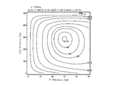
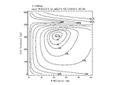
- FIG. 2 shows an antireflection unit 11 for infrared light having a wavelength ⁇ of 1550 nm, with the film thickness of the Ti film as the first metal film 12 of the semiconductor light receiving element 1A and the film thickness of the SiO2 film as the dielectric film 13 as parameters. It is the figure which plotted the result of the simulation about the reflectance of. When the thickness of the Ti film is about 30 nm and the thickness of the SiO2 film is about 300 nm, the reflectance is about 0.1%, so that the antireflection portion 11 having a low reflectance is formed.
- the reflectance is approximately 1% or less, so that the allowable film thickness range is wide and the reflection has low reflectance.
- the prevention portion 11 can be stably formed.
- the Ti film In contrast to infrared light having a wavelength ⁇ of 1100 to 1600 nm for optical communication, the Ti film has a real part (Re [n]) of a complex refractive index n of 3.4 to 3.6 and a complex refractive index of n.
- the imaginary part (Im [n]) of is 3.4 to 3.6.
- the SiO2 film has a refractive index of 1.45 to 1.44 with respect to infrared light in this region.
- the present inventor has determined Re [n] of the complex refractive index n of the first metal film 12 in order to specify the first metal film 12 capable of forming the antireflection portion 11 having a low reflectance.
- the same reflectance simulation as in FIG. 2 was performed with Im [n] as a parameter.
- the complex refractive index n of Re [n] and Im [n] of the first metal film 12 which has a wide allowable film thickness range and can stably form the antireflection portion 11 having a low reflectance. I was able to identify the range.
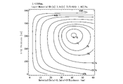
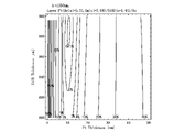
- FIG. 3 is a contour plot of the reflectance of the antireflection portion 11 when Re [n] of the complex refractive index n of the first metal film 12 is 3 and Im [n] is 3.
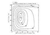
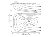
- FIG. 4 is a contour plot of the reflectance of the antireflection portion 11 when Re [n] of the complex refractive index n of the first metal film 12 is 5 and Im [n] is 5.
- the film thickness range of the first metal film 12 and the film thickness range of the SiO2 film as the dielectric film 13 are different from those in FIG. 2, but the reflectance is approximately 1% or less in both cases of FIGS. 3 and 4.
- the range of the allowable film thickness is wide, and the antireflection portion 11 having a low reflectance can be stably formed.
- Re [n] of the complex refractive index n of the first metal film 12 is 3 to 5 and Im [n] is 3 to 5
- the reflectance can be reduced to 1% or less.
- the antireflection portion 11 having a wide range of film thickness and low reflectance can be stably formed.
- a metal film using a metal material having a complex refractive index n of Re [n] and Im [n] of 3 or more as the lower limit and 5 or less as the upper limit is used as the first metal film of the antireflection portion 11. It was found that the antireflection portion 11 having a low reflectance can be obtained by setting the value to 12.
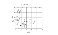
- metal materials having a complex refractive index n of Re [n] and Im [n] of 3 or more and 5 or less, respectively, for infrared light having a wavelength ⁇ of 1100 to 1600 nm used for optical communication the study was conducted. The results are shown in FIG.
- FIG. 5 is a plot of the complex refractive indexes of various metallic materials with respect to infrared light having a wavelength ⁇ of 1100 to 1600 nm. Regions where Re [n] and Im [n] of the complex refractive index n are 3 or more and 5 or less, respectively, are shown as target regions TA.
- Ti it enters the target region TA with respect to infrared light having a wavelength ⁇ of 1100 to 1600 nm.
- Cr chromium
- it enters the target region TA with respect to infrared light having a wavelength ⁇ of 1100 to 1580 nm.
- tungsten (W) it enters the target region TA with respect to infrared light having a wavelength ⁇ of 1100 to 1450 nm.
- FIG. 6 shows the reflectance when the first metal film 12 is a W film with respect to infrared light having a wavelength ⁇ of 1305 nm.
- the film thickness of the W film is about 22 +/- 4 nm and the film thickness of the SiO2 film as the dielectric film 13 is about 310 +/- 30 nm
- the antireflection portion 11 having a low reflectance can be formed.
- the antireflection portion 11 having a low reflectance can be similarly formed when the first metal film 12 is a Cr film.
- the complex refractive index of other metal materials other than Ti, Cr, and W is plotted outside the target region TA in FIG.
- the first metal film 12 is a gold film (Au film) as shown in FIG. 7
- the first metal film 12 is an aluminum film (Al film) as shown in FIG. 8 for infrared light having a wavelength ⁇ of 1550 nm.
- the range of the film thickness of the SiO2 film having a low reflectance is narrower than that of the metal material in the target region TA.
- the combination of the film thickness of the SiO2 film and the film thickness of the Au film greatly affects the reflectance.
- the antireflection portion 11 having a lower reflectance than the metal material inside the target region TA is provided. It is difficult to form it stably.
- the first metal film 12 is an Al film
- the film thickness becomes low when the reflectance is about 10 nm, but the film thickness is thinner than that of the metal material in the target region TA, which also means that the reflectance is low. It is one of the factors that makes it difficult to stably form the antireflection portion.
- the reflectance is low when the thickness of the Pt film is about 10 nm.
- the film thickness is thinner and the allowable film thickness range is as narrow as +/- 2 nm as compared with the metal material in the target region TA, antireflection having a lower reflectance than the metal material in the target region TA. It is difficult to stably form the portion 11.
- the dielectric film 13 of the antireflection portion 11 not only the SiO2 film but also the SiN film can be used.
- the refractive index of the SiN film is about 1.99, which is larger than the refractive index of 1.44 of the SiO2 film.
- the semiconductor light receiving element 1B which is a partially modified version of the first embodiment, will be described.
- the same parts as those in the first embodiment are designated by the same reference numerals as those in the first embodiment, and the description thereof will be omitted.
- the semiconductor light receiving element 1B has a first semiconductor layer 3 and a light absorption layer on the first surface 2a side of the semiconductor substrate 2 which is transparent to incident light in the infrared light region for optical communication. It has 4 and a second semiconductor layer 5.
- the second semiconductor layer 5 has a p-type diffusion region 5a.
- the region of the light absorption layer 4 in contact with the p-type diffusion region 5a corresponds to the light absorption region 4a, and the photodiode (light receiving portion 6) is formed by the p-type diffusion region 5a, the light absorption region 4a, and the first semiconductor layer 3. There is.
- the antireflection unit On the second surface 2b side of the semiconductor substrate 2, the antireflection unit reaches the irradiation region 10 where the incident light incident on the light receiving unit 6 from the first surface 2a side and transmitted through the light absorption layer 4 (light absorption region 4a) reaches. 21 is provided.
- the antireflection unit 21 is for preventing the incident light transmitted through the light absorption layer 4 (light absorption region 4a) from being reflected and incident on the light receiving unit 6 again.
- the antireflection unit 21 has a first metal film 12, a dielectric film 13, a second metal film 14, and a third metal film 22.
- the first metal film 12 is, for example, a Ti film having a thickness of 27 nm.
- the dielectric film 13 is, for example, a SiO2 film having a thickness of 270 nm, and is selectively formed in the irradiation region 10.
- the second metal film 14 is, for example, an Au film having a thickness of 600 nm.
- the third metal film 22 is, for example, a Ti film having a thickness of 3 nm, and in order to improve the adhesion between the dielectric film 13 and the second metal film 14, after the dielectric film 13 is formed and the second metal film 22 is formed. It is formed before the formation of the metal film 14.
- the third metal film 22 may be selectively formed in the same region as the dielectric film 13.
- the first metal film 12 is connected to the semiconductor substrate 2 and is connected to the second metal film 14 via the third metal film 22 on the outside of the antireflection portion 21, and the first metal film 12 and the third metal film 22 are connected.
- the second metal film 14 form the cathode electrode 19.
- the cathode electrode 19 is connected to and fixed to the wiring 18a formed on the mount substrate 18 by, for example, a conductive paste (not shown).
- the anode electrode 8 is connected to another wiring (not shown) formed on the mount substrate 18 by, for example, a bonding wire. Then, the photocurrent generated by the light receiving unit 6 is taken out from the terminal portions T1 and T2 of these wirings.
- FIG. 12 shows the antireflection unit 21 for infrared light having a wavelength ⁇ of 1550 nm, with the film thickness of the Ti film as the first metal film 12 of the semiconductor light receiving element 1B and the film thickness of the SiO2 film as the dielectric film 13 as parameters. It is the figure which plotted the result of the simulation about the reflectance of. When the thickness of the Ti film is about 27 nm and the thickness of the SiO2 film is about 270 nm, the reflectance is about 0.1%, and the antireflection portion 21 having a very low reflectance is formed.
- the reflectance is approximately 1% or less, so that the allowable film thickness range is wide and the reflection has low reflectance.
- the prevention portion 21 can be stably formed.
- Antireflection portions 11 and 21 formed by laminating a first metal film 12 having an Im [n]) of 3 or more and 5 or less, a dielectric film 13 having a refractive index of 2 or less, and a second metal film 14. It is equipped with.
- the antireflection unit 11 can prevent the light transmitted through the light absorption region 4a of the light absorption layer 4 from being reflected, it is possible to prevent the reflected light from being re-entered into the light receiving unit 6 with a simple structure. Therefore, the fall time of the semiconductor light receiving elements 1A and 1B is shortened.
- the real part (Re [n]) and the imaginary part (Im [n]) of the complex refractive index n are 3 or more and 5 respectively between the dielectric film 13 and the second metal film 14. It also has a third metal film 22 that is thinner than the first metal film 12. Therefore, the third metal film 22 can improve the adhesion between the dielectric film 13 and the second metal film 14. Therefore, it is possible to prevent the peeling of the dielectric film 13 and the second metal film 14 from forming a gap between them and deteriorating the reflection function of the antireflection portion 21.
- the first metal film 12 contains one element of titanium, chromium, and tungsten as a main component. Titanium, chromium, and tungsten have a real part (Re [n]) and an imaginary part (Im [n]) having a complex refractive index n of 3 or more and 5 or less, respectively, with respect to light in the wavelength range used for optical communication. Since it is made of the metal material of the above, it is possible to form the antireflection portions 11 and 21 having a low reflectance with respect to the incident light in the wavelength range for optical communication.
- the second metal film 14 is an Au film containing gold as a main component. Therefore, since the antireflection portions 11 and 21 can also be used as one electrode (cathode electrodes 9 and 19) of the semiconductor light receiving elements 1A and 1B, the semiconductor light receiving elements 1A and 1B having a simple structure can be formed. can.
- 1A, 1B Semiconductor light receiving element 2: Semiconductor substrate 2a: First surface 2b: Second surface 3: First semiconductor layer 4: Light absorption layer 4a: Light absorption region 5: Second semiconductor layer 5a: p-type diffusion region 6 : Light receiving part 7: Protective film 7a: Opening 8: Anode electrodes 9, 19: Cathode electrode 10: Irradiation area 11 and 21: Antireflection part 12: First metal film 13: Dielectric film 14: Second metal film 18 : Mount board 18a: Wiring 22: Third metal film T1, T2: Terminal part
Landscapes
- Light Receiving Elements (AREA)
Priority Applications (4)
| Application Number | Priority Date | Filing Date | Title |
|---|---|---|---|
| PCT/JP2021/000450 WO2022149253A1 (ja) | 2021-01-08 | 2021-01-08 | 半導体受光素子 |
| JP2021504480A JP6921457B1 (ja) | 2021-01-08 | 2021-01-08 | 半導体受光素子 |
| JP2021118892A JP7541637B2 (ja) | 2021-01-08 | 2021-07-19 | 半導体受光素子 |
| US18/347,565 US20230352604A1 (en) | 2021-01-08 | 2023-07-06 | Semiconductor light receiving device |
Applications Claiming Priority (1)
| Application Number | Priority Date | Filing Date | Title |
|---|---|---|---|
| PCT/JP2021/000450 WO2022149253A1 (ja) | 2021-01-08 | 2021-01-08 | 半導体受光素子 |
Related Child Applications (1)
| Application Number | Title | Priority Date | Filing Date |
|---|---|---|---|
| US18/347,565 Continuation US20230352604A1 (en) | 2021-01-08 | 2023-07-06 | Semiconductor light receiving device |
Publications (1)
| Publication Number | Publication Date |
|---|---|
| WO2022149253A1 true WO2022149253A1 (ja) | 2022-07-14 |
Family
ID=77269524
Family Applications (1)
| Application Number | Title | Priority Date | Filing Date |
|---|---|---|---|
| PCT/JP2021/000450 Ceased WO2022149253A1 (ja) | 2021-01-08 | 2021-01-08 | 半導体受光素子 |
Country Status (3)
| Country | Link |
|---|---|
| US (1) | US20230352604A1 (cg-RX-API-DMAC7.html) |
| JP (2) | JP6921457B1 (cg-RX-API-DMAC7.html) |
| WO (1) | WO2022149253A1 (cg-RX-API-DMAC7.html) |
Cited By (1)
| Publication number | Priority date | Publication date | Assignee | Title |
|---|---|---|---|---|
| WO2024057435A1 (ja) * | 2022-09-14 | 2024-03-21 | 株式会社京都セミコンダクター | 裏面入射型半導体受光素子 |
Families Citing this family (2)
| Publication number | Priority date | Publication date | Assignee | Title |
|---|---|---|---|---|
| JP7085786B1 (ja) * | 2022-01-19 | 2022-06-17 | 株式会社京都セミコンダクター | 半導体受光素子 |
| JP7212983B1 (ja) * | 2022-03-04 | 2023-01-26 | 株式会社京都セミコンダクター | 半導体受光素子 |
Citations (4)
| Publication number | Priority date | Publication date | Assignee | Title |
|---|---|---|---|---|
| JPS5173453A (cg-RX-API-DMAC7.html) * | 1974-12-23 | 1976-06-25 | Canon Kk | |
| JPH04218961A (ja) * | 1990-12-19 | 1992-08-10 | Fujitsu Ltd | 光電変換装置 |
| WO2015079763A1 (ja) * | 2013-11-27 | 2015-06-04 | 住友電気工業株式会社 | 受光素子 |
| US20150228680A1 (en) * | 2012-10-29 | 2015-08-13 | OmniVision Technologies, Inc., | Infrared Reflection/Absorption Layer For Reducing Ghost Image of Infrared Reflection Noise And Image Sensor Using the Same |
Family Cites Families (5)
| Publication number | Priority date | Publication date | Assignee | Title |
|---|---|---|---|---|
| JPH0720301A (ja) * | 1993-07-01 | 1995-01-24 | Matsushita Electric Ind Co Ltd | 反射防止膜 |
| JPH1096801A (ja) * | 1996-06-12 | 1998-04-14 | Asahi Glass Co Ltd | 光吸収性反射防止体およびその製造方法 |
| JP3910817B2 (ja) * | 2000-12-19 | 2007-04-25 | ユーディナデバイス株式会社 | 半導体受光装置 |
| JP2003249675A (ja) * | 2002-02-26 | 2003-09-05 | Sumitomo Electric Ind Ltd | 受光素子アレイ |
| JP2009122416A (ja) * | 2007-11-15 | 2009-06-04 | Toppan Printing Co Ltd | 光学薄膜フィルム |
-
2021
- 2021-01-08 JP JP2021504480A patent/JP6921457B1/ja active Active
- 2021-01-08 WO PCT/JP2021/000450 patent/WO2022149253A1/ja not_active Ceased
- 2021-07-19 JP JP2021118892A patent/JP7541637B2/ja active Active
-
2023
- 2023-07-06 US US18/347,565 patent/US20230352604A1/en active Pending
Patent Citations (4)
| Publication number | Priority date | Publication date | Assignee | Title |
|---|---|---|---|---|
| JPS5173453A (cg-RX-API-DMAC7.html) * | 1974-12-23 | 1976-06-25 | Canon Kk | |
| JPH04218961A (ja) * | 1990-12-19 | 1992-08-10 | Fujitsu Ltd | 光電変換装置 |
| US20150228680A1 (en) * | 2012-10-29 | 2015-08-13 | OmniVision Technologies, Inc., | Infrared Reflection/Absorption Layer For Reducing Ghost Image of Infrared Reflection Noise And Image Sensor Using the Same |
| WO2015079763A1 (ja) * | 2013-11-27 | 2015-06-04 | 住友電気工業株式会社 | 受光素子 |
Cited By (3)
| Publication number | Priority date | Publication date | Assignee | Title |
|---|---|---|---|---|
| WO2024057435A1 (ja) * | 2022-09-14 | 2024-03-21 | 株式会社京都セミコンダクター | 裏面入射型半導体受光素子 |
| JPWO2024057435A1 (cg-RX-API-DMAC7.html) * | 2022-09-14 | 2024-03-21 | ||
| JP7755755B2 (ja) | 2022-09-14 | 2025-10-16 | デクセリアルズ株式会社 | 裏面入射型半導体受光素子 |
Also Published As
| Publication number | Publication date |
|---|---|
| US20230352604A1 (en) | 2023-11-02 |
| JP2022107496A (ja) | 2022-07-21 |
| JP7541637B2 (ja) | 2024-08-29 |
| JP6921457B1 (ja) | 2021-08-18 |
| JPWO2022149253A1 (cg-RX-API-DMAC7.html) | 2022-07-14 |
Similar Documents
| Publication | Publication Date | Title |
|---|---|---|
| US20230352604A1 (en) | Semiconductor light receiving device | |
| US6894322B2 (en) | Back illuminated photodiodes | |
| US8975645B2 (en) | Optical filter | |
| Wang et al. | Hot-electron photodetector with wavelength selectivity in near-infrared via Tamm plasmon | |
| US4096387A (en) | Ultraviolet radiation detector | |
| US8975584B2 (en) | Improved-efficiency fibre-coupled terahertz system | |
| US6347107B1 (en) | System and method of improving intensity control of laser diodes using back facet photodiode | |
| CN115963376B (zh) | 发光芯片及其测试方法 | |
| CN109801984B (zh) | 背入射式光电芯片、制备方法和安装方法 | |
| JP2020053679A (ja) | ユニバーサルブロードバンド光検出器の設計及び製造方法 | |
| US12113144B2 (en) | Arrangement for an antenna for generating or receiving terahertz radiation, antenna, terahertz system, and method for producing an arrangement for an antenna | |
| US6856637B2 (en) | Optical transmitter having photodiode | |
| CN109801983B (zh) | 背入射式共面电极光电芯片及其制备方法 | |
| CN114787595B (zh) | 用于光无线功率系统安全操作的光功率计 | |
| JP2952906B2 (ja) | フォトダイオード | |
| KR101469238B1 (ko) | 적외선 광원 장치 및 이를 포함하는 가스 측정 광학계 | |
| US20240105874A1 (en) | Photodiode modules with reduced recovery times | |
| JP7085786B1 (ja) | 半導体受光素子 | |
| JP7755755B2 (ja) | 裏面入射型半導体受光素子 | |
| US20240429331A1 (en) | Semiconductor light receiving element | |
| CN112147107B (zh) | 一种反射率测试装置及测试方法 | |
| JP2008224242A (ja) | 光検出素子及びそれを用いた発光素子試験装置 | |
| KR100663588B1 (ko) | 레이저 다이오드 | |
| KR19990006168A (ko) | 포토 다이오드 및 그의 제조방법 | |
| EP1542047B1 (fr) | Dispositif focalisant pour fibres optiques et antenne à réseau de fibres optiques |
Legal Events
| Date | Code | Title | Description |
|---|---|---|---|
| ENP | Entry into the national phase |
Ref document number: 2021504480 Country of ref document: JP Kind code of ref document: A |
|
| 121 | Ep: the epo has been informed by wipo that ep was designated in this application |
Ref document number: 21917480 Country of ref document: EP Kind code of ref document: A1 |
|
| NENP | Non-entry into the national phase |
Ref country code: DE |
|
| 122 | Ep: pct application non-entry in european phase |
Ref document number: 21917480 Country of ref document: EP Kind code of ref document: A1 |