WO2022138683A1 - 光学素子 - Google Patents
光学素子 Download PDFInfo
- Publication number
- WO2022138683A1 WO2022138683A1 PCT/JP2021/047442 JP2021047442W WO2022138683A1 WO 2022138683 A1 WO2022138683 A1 WO 2022138683A1 JP 2021047442 W JP2021047442 W JP 2021047442W WO 2022138683 A1 WO2022138683 A1 WO 2022138683A1
- Authority
- WO
- WIPO (PCT)
- Prior art keywords
- base material
- optical lens
- light
- optical
- wavelength
- Prior art date
- Legal status (The legal status is an assumption and is not a legal conclusion. Google has not performed a legal analysis and makes no representation as to the accuracy of the status listed.)
- Ceased
Links
Images










Classifications
-
- G—PHYSICS
- G02—OPTICS
- G02B—OPTICAL ELEMENTS, SYSTEMS OR APPARATUS
- G02B1/00—Optical elements characterised by the material of which they are made; Optical coatings for optical elements
- G02B1/10—Optical coatings produced by application to, or surface treatment of, optical elements
- G02B1/11—Anti-reflection coatings
-
- G—PHYSICS
- G02—OPTICS
- G02B—OPTICAL ELEMENTS, SYSTEMS OR APPARATUS
- G02B3/00—Simple or compound lenses
-
- G—PHYSICS
- G02—OPTICS
- G02B—OPTICAL ELEMENTS, SYSTEMS OR APPARATUS
- G02B5/00—Optical elements other than lenses
- G02B5/20—Filters
- G02B5/22—Absorbing filters
Definitions
- the present invention relates to an optical element.
- Ultraviolet curable resin is widely used for optical lenses used in mobile phones, digital cameras, etc.
- a wafer level lens is manufactured by molding a plurality of lenses on a substrate using an ultraviolet curable resin, and a lens module is manufactured by cutting the substrate and separating the plurality of lenses.
- a duplication tool that defines the shape of the lens is used, and the uncured duplication material is UV-cured while the uncured duplication material (ultraviolet curable material) is sandwiched between the duplication tool and the substrate.
- a method of forming a lens is known (Patent Document 1).
- the ultraviolet curable resin (uncured) is partially irradiated with ultraviolet rays to cure it.
- the extra portion as a lens is not irradiated with ultraviolet rays, and after the curing step, the ultraviolet curable resin in the uncured portion is removed by cleaning.
- the ultraviolet curable resin when the ultraviolet curable resin is cured in the exposed portion of ultraviolet rays, the curing of the ultraviolet curable resin may proceed in the unexposed portion, and the outer diameter of the formed lens is stable. It tends to be inferior in sex.
- One aspect of the present invention has been made in view of the above problems, and an object of the present invention is to provide an optical element that suppresses a decrease in outer diameter dimensional stability.
- the optical element according to the present disclosure supports an optical lens made of an ultraviolet curable resin and the optical lens, and has an absorption rate of light having a wavelength of 365 nm of 50% or more.
- the optical lens has a projected area of 2000 mm 2 or less, which is an area when the optical lens is projected onto a plane orthogonal to the optical axis direction of the optical lens. Is projected radially outward from the peripheral edge of the optical lens over the entire circumference of the peripheral edge of the optical lens when viewed from the optical axis direction of the optical lens.
- the optical element according to the present disclosure supports an optical lens made of an ultraviolet curable resin, the optical lens, a base material portion, and the base material portion.
- the base material has a base material containing a functional film that suppresses the reflection of ultraviolet rays, and is made of a material different from the base material portion. be.
- an optical element in which a decrease in outer diameter dimensional stability is suppressed.
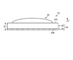
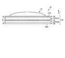
- FIG. 1A is a schematic diagram of an optical element according to the first embodiment.
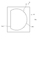
- FIG. 1B is a top view of the optical element according to the first embodiment.
- FIG. 1C is an enlarged view of the peripheral edge and the vicinity of the peripheral edge of the optical lens according to the first embodiment.
- FIG. 2 is a schematic diagram illustrating the transmittance.
- FIG. 3 is a schematic diagram illustrating the reflectance.
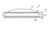
- FIG. 4 is a schematic diagram of an optical element according to another example of the first embodiment.
- FIG. 5 is a schematic diagram illustrating a method for manufacturing an optical element.
- FIG. 6 is a schematic diagram illustrating a method for manufacturing an optical element.
- FIG. 7 is a schematic diagram illustrating a method for manufacturing an optical element.
- FIG. 5 is a schematic diagram illustrating a method for manufacturing an optical element.
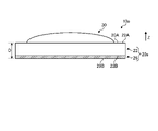
- FIG. 16 is a schematic diagram of the optical element according to the second embodiment.
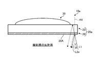
- FIG. 17 is a schematic diagram illustrating the reflectance of the functional film.
- FIG. 18 is a schematic diagram of an optical element according to another example of the second embodiment.
- FIG. 19 is a schematic diagram showing another example of the shape of the optical lens.
- FIG. 20 is a schematic diagram showing another example of the shape of the optical lens.
- FIG. 21 is a schematic diagram showing another example of the shape of the optical lens.
- the optical element 10 may be an element in which one optical lens is provided on one substrate, or an element in which a plurality of optical lenses are provided on one substrate. It is also good.
- the optical element 10 may be an element in which optical lenses are provided on both sides of a base material.
- the optical element 10 may be provided with one optical lens on each side of one substrate, or may be provided with a plurality of optical lenses on both sides of one substrate.
- one optical lens may be provided on one surface of one substrate, and a plurality of optical lenses may be provided on the other surface.
- the optical lenses are provided on both sides of the substrate, it is preferable that the optical lenses are provided so that the optical axis positions of the optical lenses on both sides are the same.
- Examples of the monomer, oligomer, reactive polymer and the like having a cationically polymerizable bond include compounds having an epoxy group, an oxetanyl group, an oxazolyl group, a vinyloxy group and the like.
- (Meta) acryloyl group means an acryloyl group or a meta-acryloyl group.
- (meth) acrylate is meant acrylate or methacrylate.
- conventionally used ones can be used as the type of the photopolymerization initiator according to the present embodiment.
- the projected area of the optical lens 30 on the plane when the optical lens 30 is projected on the direction Z side with respect to the plane orthogonal to the direction Z (optical axis direction) is defined as the projected area. That is, it can be said that the projected area of the optical lens 30 refers to the area of the optical lens 30 when viewed from the direction Z side as shown in FIG. 1B.
- the projected area of the optical lens 30 is preferably 2000 mm 2 or less, 500 mm 2 or less, 30 mm 2 or less, 5 mm 2 or less, and 1 mm 2 or less. It may be.
- the projected area of the optical lens 30 may be 0.002 mm 2 or more, 0.01 mm 2 or more, or 0.1 mm 2 or more.
- the projected area of the optical lens 30 may be 0.002 mm 2 or more and 2000 mm 2 or less, 0.01 mm 2 or more and 500 mm 2 or less, and 0.1 mm 2 or more and 30 mm 2 or less. It may be 0.1 mm 2 or more and 5 mm 2 or less, and may be 0.1 mm 2 or more and 1 mm 2 or less. When the size of the optical lens 30 is within this range, the optical element can be miniaturized.
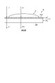
- an arbitrary position on the peripheral edge 30a is defined as the first position PA, and the position on the surface of the optical lens 30 on the Z-direction side, which is radially inward from the first position PA by a distance W2, is the second position.
- the distance W2 is 20 ⁇ m, in other words, it can be said that the second position PC is a position 20 ⁇ m inward in the radial direction from the first position PA.
- the distance in the Z direction from the first position PA to the second position PC that is, the distance in the Z direction from the support surface 20A of the base material 20 to the second position PC is defined as the distance W3.
- the profile of the surface of the optical lens 30 on the Z direction side from the first position PA to the second position PC along the inner side in the radial direction is referred to as a lens profile
- the approximate straight line of the lens profile is referred to as an approximate straight line LP.
- the lens profile can be said to be a profile showing the position of the surface of the optical lens 30 on the Z direction side in the Z direction from the first position PA to the second position PC.
- the angle ⁇ formed by the approximate straight line LP and the support surface 20A of the base material 20 is preferably 45 ° or more, more preferably 50 ° or more, and further preferably 55 ° or more.
- the angle ⁇ can also be said to be an angle formed by the approximate straight line LP and the straight line on the support surface 20A along the inner side in the radial direction (the inclination angle of the approximate curve LP with respect to the support surface 20A).
- a commercially available coordinate measuring machine is used for measuring the lens profile. Specifically, for example, an optical component shape measuring machine (trade name: PGI matrix) manufactured by Taylor Hobson Co., Ltd. is used. The tip diameter (radius) of the contact needle is 5 ⁇ m.
- the approximate straight line is obtained by approximating the lens profile, that is, the position of the surface of the optical lens 30 on the Z direction side from the position PA to the position PC in the Z direction by the method of least squares.
- the base material 20 includes the base material portion 22 and the absorption film 24.
- the base material portion 22 may be made of any material.
- the base material portion 22 may be at least one of a resin base material made of resin, a glass base material made of glass, and a crystal base material made of a crystal material.
- the resin that can be used for the base material portion 22 includes polyester resins such as polyethylene terephthalate and polybutylene terephthalate, polyolefin resins such as polyethylene, polypropylene and ethylene vinyl acetate copolymer, norbornene resin, polyacrylate and polymethylmethacrylate.
- the "phosphate glass” also includes a silicate glass in which a part of the skeleton of the glass is composed of SiO 2 .
- the crystal material that can be used for the base material portion 22 among calcium fluoride, sapphire, zinc selenium, silicon, germanium, barium fluoride, lithium fluoride, magnesium fluoride, crystal, lithium niobate and the like. At least one is mentioned.
- a resin material, glass, and a crystal material may be used alone for the base material portion 22, or two or more kinds of the same or different materials may be laminated and used.
- the material of the base material portion 22 is not particularly limited, and the characteristics of the base material 20 described later can be realized by adjusting, for example, the thickness of the base material and the manufacturing method, even if the material is other than the above-exemplified materials.
- the absorption film 24 has a function of absorbing light (ultraviolet rays) having a wavelength of 365 nm.
- the absorption film 24 is composed of a member having a higher absorption degree of light having a wavelength of 365 nm than that of the base material portion 22, but the absorption film 24 is not limited to this, and even if the absorption degree of light having a wavelength of 365 nm is equivalent to that of the base material portion 22. It may be smaller than the base material portion 22.
- the absorbent film 24 contains at least a material that absorbs light having a wavelength of 365 nm (hereinafter referred to as an absorbent material).
- the absorption film 24 may further include a matrix (hereinafter referred to as a matrix) carrying a material that absorbs light having a wavelength of 365 nm.
- the absorbing material is not particularly limited as long as it is a material that absorbs light having a wavelength of 365 nm.
- the absorbent material include a dye or pigment made of an organic material, a pigment made of a metal oxide, and an organometallic complex.
- the organic material-based absorbent material include at least one of benzophenone-based, benzotriazole-based, dibenzoylmethane-based, oxalic acid anilides-based, cyanoacrylate-based, triazine-based, and coumarin-based derivatives. ..
- Examples of the metal oxide-based absorbing material include at least one of zinc oxide, titanium oxide, cerium oxide, iron oxide and the like.
- Examples of the organometallic complex-based absorbing material include a complex composed of at least one of zinc (II) ion, copper (II) ion and the like.
- the organic ligand of the complex is not limited as long as it is considered to form a complex structure from the composition.
- As the absorbent material contained in the absorbent membrane 24, one of the exemplified absorbent materials may be used alone, or two or more of them may be mixed and used.
- the matrix has the function of supporting an absorbent material that is in a molecular or fine particle state. As the matrix, the resin and glass exemplified in the base material portion 22 can be used.
- the absorption film 24 and the base material portion 22 are prepared as a single base material, and then the absorption film 24 and the base material portion 22 are provided with an optical adhesive.
- the absorbent film 24 and the base material portion 22 may be directly bonded to each other.
- the transmittance is measured while avoiding the formation.
- the partial formation include printing (marking) such as an aperture and an identification number.
- the light transmittance can be measured by measuring the spectral transmittance curve using, for example, an ultraviolet-visible spectrophotometer (Hitachi High-Tech Corporation (UH4150 type)). Unless otherwise specified, the light transmittance of the base material 20 refers to those measured by the same method thereafter.
- the measurement point of the base material has an area equal to or less than the measurement limit of the ultraviolet-visible spectrophotometer, it can be measured by the microspectroscopy method.
- the reflectance of the light of the base material 20 is the light L1 reflected by the base material 20 with respect to the intensity of the light L1 irradiated to the portion of the base material 20 that does not overlap with the optical lens 30 as shown in FIG.
- the reflected light L3 here is the light reflected by the incident surface of the light L1 (support surface 20A in the example of FIG. 3) and the light reflected by the exit surface of the light L1 (plane 20B in the example of FIG. 3). include.
- the reflected light L3 is the light reflected on the incident surface of the light L1 and the light reflected on the exit surface of the light L1 as well as the light reflected on the base material 20. It also includes light reflected between layers (in the example of FIG. 3, the interface between the base material portion 22 and the absorption film 24 described later).
- the light L1 used for measuring the light reflectance of the base material 20 was tilted by 5 ° with respect to the axis AX orthogonal to the incident surface (support surface 20A in the example of FIG. 2) of the light L1 of the base material 20. Irradiated in the direction. That is, ⁇ in FIG. 3 is 5 °.
- the light L1 becomes light having a wavelength of 365 nm.
- the reflectance is measured while avoiding the formation. Examples of the partial formation include printing (marking) such as an aperture and an identification number.
- the reflectance of light can be measured by measuring the spectral transmittance curve using, for example, an ultraviolet-visible spectrophotometer (Hitachi High-Tech Corporation (UH4150 type)). Unless otherwise specified, the light reflectance of the base material 20 refers to those measured by the same method thereafter. When the measurement point of the base material has an area equal to or less than the measurement limit of the ultraviolet-visible spectrophotometer, it can be measured by the microspectroscopy method.
- the substrate 20 preferably has an absorption rate of light having a wavelength of 365 nm of 50% or more, more preferably 65% or more, further preferably 90% or more, and particularly preferably 99% or more. preferable.
- the light absorption rate of the base material 20 is calculated by the following formula (1).
- A is the light absorption rate of the base material 20
- A1 is the light transmittance of the base material 20
- A2 is the light reflectance of the base material 20.
- the absorption rate of light having a wavelength of 365 nm of the base material 20 is a value obtained by subtracting the transmittance of light having a wavelength of 365 nm of the base material 20 and the reflectance of light having a wavelength of 365 nm of the base material 20 from 100.
- A 100- (A1 + A2) ... (1)
- FIG. 4 is a schematic diagram of an optical element according to another example of the first embodiment.
- the antireflection film 26 may be formed on the base material 20.
- the antireflection film 26 is an AR (Anti Reflection) film that suppresses the reflection of at least one of visible light and infrared light.
- the antireflection film 26 is provided on the direction Z side of the base material portion 22 and on the side opposite to the direction Z of the base material portion 22.
- the antireflection film 26 on the direction Z side of the base material portion is formed on the direction Z side of the absorption film 24, that is, on the surface of the absorption film 24 on the direction Z side, but is not limited thereto, for example, the base material portion. It may be formed between 22 and the absorption film 24. Further, the antireflection film 26 is not limited to being provided on both the direction Z side of the base material portion 22 and the side opposite to the direction Z of the base material portion 22, but also on the direction Z side of the base material portion 22 and the base. It may be provided on either side of the material portion 22 on the opposite side to the direction Z.
- the antireflection film 26 may be made of any material as long as it suppresses the reflection of at least one of visible light and infrared light.
- a high refractive index material and a low refractive index material are alternately used. It is composed of laminated dielectric multilayer films.
- the high refractive index material is preferably a material having a refractive index of 1.7 or more, and more preferably 2.2 or more and less than 2.5.
- As the high refractive index material for example, ZrO 2 , Ta 2 O 5 , TiO 2 , Nb 2 O 5 and the like are used.
- the low refractive index material is preferably a material having a refractive index of less than 1.7, more preferably a material having a refractive index of 1.45 or more and less than 1.55, and further preferably a material having a refractive index of 1.45 or more and less than 1.47. ..
- Examples of the low refractive index material include SiO 2 , SiO x N y , and MgF 2 .
- X and Y may be arbitrary numerical values.
- the antireflection film 26 may be composed of, for example, a single-layer film such as SiO 2 or Al 2 O 3 .
- the antireflection film 26 may be formed by forming a dielectric material into a film by vacuum deposition such as vacuum deposition, sputtering, and CVD.
- the substrate 20 has an average transmittance of light having a wavelength of 450 nm or more and 600 nm or less, preferably 70% or more, more preferably 80% or more, further preferably 90% or more, and 95% or more. Is particularly preferable.
- the average transmittance when the antireflection film 26 is provided is in the above range, but the average transmittance when the antireflection film 26 is not provided may also be in the above range.
- the transmittance of visible light having a wavelength of 450 nm or more and 600 nm or less is within this range, the characteristics of the optical element 10 for visible light can be ensured.
- the average transmittance of light having a wavelength of 450 nm or more and 600 nm or less is an average value of the transmittance of light having a wavelength of 450 nm to 600 nm.
- the average transmittance also refers to the average value of the transmittance of light of each wavelength unless otherwise specified.
- the substrate 20 has an average reflectance of light having a wavelength of 450 nm or more and 600 nm or less, preferably 10% or less, more preferably 5% or less, still more preferably 1% or less, and 0.5. It is more preferably% or less, and particularly preferably 0.1% or less.
- the average reflectance when the antireflection film 26 is provided is in the above range, but the average reflectance when the antireflection film 26 is not provided may also be in the above range.
- the reflectance of visible light having a wavelength of 450 nm or more and 600 nm or less is within this range, the characteristics of the optical element 10 for visible light can be ensured.
- the average reflectance of light having a wavelength of 450 nm or more and 600 nm or less is an average value of the transmittance of light having a wavelength of 450 nm to 600 nm.
- the average reflectance also refers to the average value of the reflectance of light of each wavelength unless otherwise specified.
- the substrate 20 has an average transmittance of light having a wavelength of 930 nm or more and 950 nm or less, preferably 70% or more, more preferably 80% or more, further preferably 90% or more, and further preferably 95% or more. Is particularly preferable.
- the average transmittance when the antireflection film 26 is provided is in the above range, but the average transmittance when the antireflection film 26 is not provided may also be in the above range.
- the transmittance of infrared light having a wavelength of 930 nm or more and 950 nm or less is within this range, the characteristics of the optical element 10 for infrared light can be ensured.
- the substrate 20 has an average reflectance of light having a wavelength of 930 nm or more and 950 nm or less, preferably 10% or less, more preferably 5% or less, still more preferably 1% or less, and 0.5. It is more preferably% or less, and particularly preferably 0.1% or less.
- the average reflectance when the antireflection film 26 is provided is in the above range, but the average reflectance when the antireflection film 26 is not provided may also be in the above range.
- the reflectance of infrared light having a wavelength of 930 nm or more and 950 nm or less is within this range, the characteristics of the optical element 10 for infrared light can be ensured.
- the optical element 10 preferably has an average transmittance of 70% or more, more preferably 80% or more, further preferably 90% or more, and 95% or more, of light having a wavelength of 450 nm or more and 600 nm or less. It is particularly preferable to have. When the transmittance of visible light having a wavelength of 450 nm or more and 600 nm or less is within this range, the characteristics of the optical element 10 for visible light can be ensured. As shown in FIG. 2, the light transmittance of the optical element 10 refers to the light transmittance of the portion where the base material 20 and the optical lens 30 overlap.
- the light transmittance of the optical element 10 means that the base material 20 and the optical lens 30 are transmitted with respect to the intensity of the light L0 irradiated to the portion where the base material 20 and the optical lens 30 overlap, as shown in FIG. It refers to the ratio of the intensity of light L0a, which is light L0.
- the light L0 is emitted in the direction along the optical axis of the optical lens 30.
- the light L1 is light having a wavelength of 450 nm or more and 600 nm or less.
- the optical element 10 preferably has an average transmittance of 70% or more, more preferably 80% or more, further preferably 90% or more, and 95% or more, of light having a wavelength of 930 nm or more and 950 nm or less. It is particularly preferable to have. When the transmittance of infrared light having a wavelength of 930 nm or more and 950 nm or less is within this range, the characteristics of the optical element 10 for infrared light can be ensured.
- a method of manufacturing the optical element 10 Next, a method of manufacturing the optical element 10 will be described.
- a step of preparing the base material 20 and a step of arranging an uncured ultraviolet curable resin 30A on the surface (support surface 20A) on the direction Z (first direction) side of the base material 20 are included.
- the uncured ultraviolet curable resin 30A is cured to form an optical lens 30.
- steps to do a part of the surface of the uncured ultraviolet curable resin 30A on the direction Z side is covered with a shielding portion that shields ultraviolet rays.
- the ultraviolet rays may have any wavelength as long as they can cure the ultraviolet curable resin 30A, but in the present embodiment, they are 365 nm.
- FIGS. 5 to 9 are schematic views illustrating a method for manufacturing an optical element.
- a plurality of optical lenses 30 are formed on the large base material 20, and the optical lenses 30 are formed on the base material 20 by cutting each optical lens 30.
- the present invention is not limited to this, and one optical lens 30 may be formed on the base material 20 to manufacture one optical element 10.
- optical lenses may be formed on both sides of the base material 20.
- one side may be manufactured according to FIGS. 5 to 9, and then an optical lens may be manufactured on the other side according to FIGS. 5 to 9.
- the optical lenses are provided on both sides of the substrate, they may be formed so that the optical axis positions of the optical lenses on both sides are the same.
- the method for manufacturing the optical element 10 of the present embodiment includes, for example, the following steps (a) to (d).
- a plurality of molding portions 160 are provided on the plate-shaped portion 140, and a recess 120 is formed on the upper surface of the molding portion 160. That is, the recess 120 refers to the recess formed on the upper surface of the molded portion 160.
- a shielding portion 180 that blocks the transmission of ultraviolet rays is provided between the recesses 120 of the adjacent molding portions 160 in the surface layer portion on the molding portion 160 side of the plate-shaped portion 140.
- the shape and outer diameter of the recess 120 correspond to the shape of the optical lens 30.
- a translucent material As a material for forming the portion of the plate-shaped portion 140 other than the shielding portion 180 and the molding portion 160 in the mold 100, a translucent material can be exemplified.
- a non-transmissive material can be exemplified.
- the translucent material include a cured product of an acrylic ultraviolet curable resin, glass such as quartz glass, polydimethylsiloxane, cyclic polyolefin, polycarbonate, polyethylene terephthalate, and transparent fluororesin.
- the non-transmissive material include chromium, nickel, copper, titanium, oxides thereof, silicon carbide, and mica.
- Examples of the method for arranging the uncured ultraviolet curable resin 30A in the recess 120 of the mold 100 in the step (a) include an inkjet method, a potting method (dispensing method), a spin coating method, a roll coating method, a casting method, and a dip. Examples include the coating method, the die coating method, and the Langmüller project method.
- the press pressure (gauge pressure) when sandwiching the uncured ultraviolet curable resin 30A between the mold 100 and the base material 20 is preferably more than 0 MPa and 10 MPa or less, preferably 0.1 MPa to 5 MPa. Is more preferable.
- the numerical range represented by "-" means a numerical range including the numerical values before and after ... as the lower limit value and the upper limit value.
- the temperature at which the uncured ultraviolet curable resin 30A is sandwiched between the mold 100 and the base material 20 is preferably 0 ° C to 110 ° C, more preferably 10 ° C to 80 ° C.
- ultraviolet rays are irradiated from the side opposite to the shielding portion 180 of the plate-shaped portion 140 in the mold 100.
- Ultraviolet rays are transmitted from between the shielding portions 180 and partially irradiate each uncured ultraviolet curable resin 30A.
- the uncured ultraviolet curable resin 30A is cured to form the optical lens 30. Since the ultraviolet rays are blocked by the shielding portion 180 between the adjacent recesses 120, it becomes an unexposed portion. Therefore, in the unexposed portion between the adjacent recesses 120, the curing of the uncured ultraviolet curable resin 30A is suppressed.
- Examples of the light source of ultraviolet rays include UV-LED, low-pressure mercury lamp, high-pressure mercury lamp, and ultra-high-pressure mercury lamp.
- the irradiation amount of ultraviolet rays is preferably 100 mJ / cm 2 to 30,000 mJ / cm 2 , more preferably 1,000 mJ / cm 2 to 20,000 mJ / cm 2 .
- the mold 100 is separated, and the uncured ultraviolet curable resin 30A in the unexposed portion shown in FIG. 8 is washed and removed.
- a wafer level lens 1 in which a plurality of optical lenses 30 are provided on the base material 20 is obtained.
- the wafer level lens 1 is divided into each optical lens 30, and a plurality of optical elements 10 are obtained.
- the temperature at which the optical lens 30 and the mold 100 are separated is preferably 0 ° C to 110 ° C, more preferably 10 ° C to 80 ° C.
- the cleaning method include spin cleaning, dip cleaning, and ultrasonic cleaning.
- an uncured ultraviolet curable resin provided on a substrate is exposed to ultraviolet rays and cured to obtain a desired shape.
- the ultraviolet curable resin may be cured even in the unexposed portion (the portion shielded by the shielding portion) to which the ultraviolet rays are not exposed, and the outer diameter dimensional stability of the optical lens may be deteriorated.
- the cause of the progress of curing of the ultraviolet curable resin in the unexposed portion is that the ultraviolet rays incident on the ultraviolet curable resin are reflected on the surface opposite to the optical lens of the base material and stray light.
- the optical element 10 according to the present embodiment includes the base material 20 having an absorption rate of light having a wavelength of 365 nm of 50% or more.
- the optical element 10 according to the present embodiment absorbs ultraviolet rays by the base material 20 to prevent the ultraviolet rays from being reflected and reaching the unexposed portion as stray light. Therefore, in the optical element 10 according to the present embodiment, a decrease in outer diameter dimensional stability is suppressed.
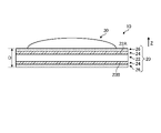
- FIG. 10 to 15 are schematic views of an optical element according to another example of the first embodiment.
- the absorption film 24 may be provided on the surface 22B on the side opposite to the direction Z of the base material portion 22 (the side opposite to the optical lens 30). Further, the base material 20 may be provided with the absorption film 24 on both the surface 22A of the base material portion 22 and the surface 22B of the base material portion 22. That is, the configurations of FIG. 1A and FIG. 10 may be combined. From the viewpoint of outer diameter dimensional stability, the absorbent film 24 is provided on the surface 22A side of the base material portion 22 rather than on the surface 22B side, or is provided inside the base material portion 22 as described later. It is more preferable that it is provided.
- the base material 20 may be provided with the antireflection film 26 even in a configuration in which the absorption film 24 is arranged on the side opposite to the direction Z of the base material portion 22.
- the antireflection film 26 is provided on the direction Z side of the base material portion 22 and on the side opposite to the direction Z of the base material portion 22.
- the antireflection film 26 on the side opposite to the direction Z of the base material portion 22 is formed on the surface on the side opposite to the direction Z of the absorption film 24, but is not limited thereto, for example, the base material portion 22 and the absorption film. It may be formed between 24 and 24.
- the antireflection film 26 is not limited to being provided on both the direction Z side of the base material portion 22 and the side opposite to the direction Z of the base material portion 22, but also on the direction Z side of the base material portion 22 and the base. It may be provided on either side of the material portion 22 on the opposite side to the direction Z.
- FIG. 12 shows a configuration example in which the absorption film 24 is arranged on both the surface 22A and the surface 22B of the base material portion 22 and the antireflection film 26 is provided.
- the antireflection film 26 is provided on the direction Z side of the base material portion 22 and on the opposite side of the base material portion 22 in the direction Z.
- the antireflection film 26 on the direction Z side of the base material portion 22 is formed on the direction Z side of the absorption film 24, but is not limited to this, and is formed between the base material portion 22 and the absorption film 24, for example. May be.
- the antireflection film 26 on the side opposite to the direction Z of the base material portion 22 is formed on the side opposite to the direction Z of the absorption film 24, but is not limited thereto, for example, the base material portion 22 and the absorption film. It may be formed between 24 and 24. Further, the antireflection film 26 is not limited to being provided on both the direction Z side of the base material portion 22 and the side opposite to the direction Z of the base material portion 22, but also on the direction Z side of the base material portion 22. It may be provided on either side of the base material portion 22 on the side opposite to the direction Z.
- the absorption film 24 may be provided inside the base material portion 22. That is, the base material portion 22 is provided with the base material portion 22S on the direction Z side and the base material portion 22T on the opposite side to the direction Z, and the absorption film 24 is composed of the base material portion 22S and the base material portion 22T. It may be provided between them.
- the base material 20 may be provided with the antireflection film 26 even in a configuration in which the absorption film 24 is arranged inside the base material portion 22.
- the antireflection film 26 is provided on the direction Z side of the base material portion 22 and on the side opposite to the direction Z of the base material portion 22.
- the antireflection film 26 is not limited to being provided on both the direction Z side of the base material portion 22 and the side opposite to the direction Z of the base material portion 22, but also on the direction Z side of the base material portion 22 and the base material portion. It may be provided on either side of the direction Z of 22 and the opposite side.
- the base material 20 has a structure in which the base material portion 22 and the absorption film 24 that absorbs ultraviolet rays are laminated, but the base material portion itself is provided with a function of absorbing ultraviolet rays. You may.
- the base material 20 includes the base material portion 22a.
- the base material portion 22a has a function of absorbing light (ultraviolet rays) having a wavelength of 365 nm.
- the base material portion 22a supports the optical lens 30 on the surface 22A with the surface 22A as the support surface 20A. It can be said that the base material portion 22a also has a function as an absorption film 24.
- the resin that can be used as the base material portion 22a is one of the resins having the property of absorbing ultraviolet rays in the base material portion 22, and is, for example, an acrylic resin such as polyacrylate and polymethylmethacrylate, an epoxy resin, a polycarbonate resin, and a poly. It is at least one of etherimide resin, polysulfone resin, polyether sulfone resin and the like. Further, the resin base material that can be used as the base material portion 22 or the base material portion 22a described above may be in a form in which an organic material, an inorganic oxide or a metal complex that can be used as the absorption film 24 described above is supported.
- the base material portion 22 or the base material portion 22a may have the same configuration as the absorption film 24.
- the glass that can be used as the base material portion 22a is one of the glass having the property of absorbing ultraviolet rays among the base material portions 22, and is, for example, at least one such as barium-based glass, lanthanum-based glass, and flint-based glass. It is a seed.
- the glass that can be used as the base material portion 22a include crown-based glass that absorbs ultraviolet rays, in addition to the above-mentioned glass.
- the glass may be in the form in which an organic material, an inorganic oxide or a metal complex that can be used as the above-mentioned absorption film 24 is supported.
- the base material portion 22 or the base material portion 22a may have the same configuration as the absorption film 24.
- the crystalline material that can be used as the base material portion 22a is one of the crystalline materials having the property of absorbing ultraviolet rays among the base material portions 22, and is, for example, zincated selenium, silicon, and the like.
- the base material portion 22a is not limited to the material. That is, the material of the base material portion 22a may be a material other than the above-mentioned examples as the base material portion 22a.
- the function of absorbing ultraviolet rays can be imparted to the base material portion 22 by adjusting the thickness of the base material portion 22 and the manufacturing method, and the absorption rate of light having a wavelength of 365 nm of the base material 20 is 50% or more. be able to.
- the base material 20 may include the base material portion 22a and the antireflection film 26.
- the antireflection film 26 is provided on the direction Z side of the base material portion 22a and on the side opposite to the direction Z of the base material portion 22a.
- the antireflection film 26 is not limited to being provided on both the direction Z side of the base material portion 22a and the side opposite to the direction Z of the base material portion 22a, and the antireflection film 26 is provided on the direction Z side of the base material portion 22. It may be provided on either side of the base material portion 22 on the side opposite to the direction Z.
- the base material 20 may be configured to have both the base material portion 22a and the absorption film 24.
- the base material 20 can more preferably absorb ultraviolet rays by providing the base material portion 22a and the absorbing film 24.
- the layer structure when the base material portion 22a and the absorption film 24 are provided may be the same as the layer structure when the base material portion 22 and the absorption film 24 described above are provided.
- the optical element 10 supports an optical lens 30 made of an ultraviolet curable resin and an optical lens 30, and has a substrate having a light absorption rate of 50% or more at a wavelength of 365 nm. 20 and.
- the optical lens 30 has a projected area of 2000 mm 2 or less, which is an area when the optical lens 30 is projected on a plane orthogonal to the Z direction (the optical axis direction of the optical lens 30).
- the base material 20 has a region protruding radially outward from the peripheral edge 30a of the optical lens 30 when viewed from the Z direction (optical axis direction of the optical lens 30).
- an optical lens made of an ultraviolet curable resin an optical lens having a desired shape is manufactured by exposing the uncured ultraviolet curable resin provided on the substrate to ultraviolet rays and curing the lens. ..
- the UV curable resin may be cured even in the unexposed part (the part shielded by the shield part) that is not exposed to ultraviolet rays, and the outer diameter dimensional stability of the optical lens may be deteriorated. rice field.
- the optical element 10 according to the present embodiment is provided with the base material 20 having an absorption rate of light having a wavelength of 365 nm of 50% or more, thereby suppressing the reflection of ultraviolet rays and reaching the unexposed portion.
- the optical element 10 according to the present embodiment, a decrease in outer diameter dimensional stability is suppressed.
- the projected area of the optical lens 30 is as small as 2000 mm 2 or less, the size of the optical element 10 is suppressed from becoming large, and the base material 20 projects outward from the optical lens 30 to obtain optics.
- the lens 30 can be appropriately supported.
- the projected area of the optical lens 30 is as small as 2000 mm 2 or less, when the unexposed portion is cured, the area of the cured portion becomes relatively large, so that the unexposed portion is cured.
- the effect on outer diameter dimensional stability is particularly large. This embodiment is particularly effective in reducing the outer diameter dimensional stability by appropriately suppressing the curing of the unexposed portion by the base material 20 for such a small optical lens 30.
- the substrate 20 preferably has a light absorption rate of 65% or more at a wavelength of 365 nm.
- the optical element 10 according to the present embodiment suppresses the reflection of ultraviolet rays and reaches the unexposed portion, and more preferably suppresses the deterioration of the outer diameter dimensional stability. do.
- the base material 20 preferably has an average transmittance of 70% or more for light having a wavelength of 450 nm or more and 600 nm or less.
- the optical element 10 according to the present embodiment can ensure the characteristics of the optical element 10 for visible light.
- the base material 20 preferably has an average transmittance of 70% or more for light having a wavelength of 930 nm or more and 950 nm or less.
- the optical element 10 according to the present embodiment can ensure the characteristics of the optical element 10 for infrared light.
- the base material 20 may include a base material portion 22a that absorbs light having a wavelength of 365 nm.
- the optical element 10 according to the present embodiment can suitably suppress the reflection of ultraviolet rays and reaching the unexposed portion.
- the base material 20 may include a base material portion 22 that transmits light having a wavelength of 365 nm and an absorption film 24 that absorbs light having a wavelength of 365 nm.
- the optical element 10 can improve the degree of freedom in selecting the material of the base material portion 22 while suppressing the reflection of ultraviolet rays.
- the absorption film 24 may be provided on the surface 22A of the base material portion 22 on the side where the optical lens 30 is provided. By providing the absorption film 24 at this position, it is possible to suitably suppress the reflection of ultraviolet rays and reaching the unexposed portion.
- the absorption film 24 may be provided between the base material portion 22 and the optical lens 30. By providing the absorption film 24 at this position, it is possible to suitably suppress the reflection of ultraviolet rays and reaching the unexposed portion.
- the absorption film 24 may be provided inside the base material portion 22. By providing the absorption film 24 at this position, it is possible to suitably suppress the reflection of ultraviolet rays and reaching the unexposed portion.
- the optical lens 30 includes a first position PA that is an arbitrary position on the peripheral edge 30a, and a second position PC on a surface that is 20 ⁇ m inward in the radial direction when the optical axis direction is the axial direction from the first position PA.
- the distance W3 in the optical axis direction between them may be 20 ⁇ m or more. Since the optical member 10 according to the present embodiment can suppress the ultraviolet rays from reaching the unexposed portion by the base material 20, the optical lens 30 having a shape in the vicinity of the peripheral edge 30a can be formed in this way. It is possible to suppress an increase in the size of the element 10.
- the absorption film 24 may be provided on the surface 22B of the base material portion 22 on the side opposite to the side on which the optical lens 30 is provided. By providing the absorbent film 24 at this position, it is possible to suppress the influence on the adhesion between the base material 20 and the optical lens 30 while suppressing the reflection of ultraviolet rays.
- the second embodiment is different from the first embodiment in that the base material 20a has a functional film 28 that suppresses the reflection of ultraviolet rays.
- the description of the parts having the same configuration as that of the first embodiment will be omitted.
- FIG. 16 is a schematic diagram of the optical element according to the second embodiment.
- the optical element 10a according to the second embodiment has a base material 20a and an optical lens 30.
- the base material 20a has a base material portion 22 and a functional film 28.
- the functional film 28 is a so-called ultraviolet AR film having a function of suppressing reflection of light (ultraviolet rays) having a wavelength of 365 nm.
- the functional film 28 is made of a material different from that of the base material portion 22.
- a dielectric multilayer film in which low refractive index materials and high refractive index materials are alternately laminated can be used.
- a single layer of a low refractive index material such as SiO 2 , SiO x Ny , and MgF 2 may be used as the functional film 28.
- the functional film 28 is a film having a light reflection suppressing function having a wavelength of 365 nm, but may have other functions.
- the functional film 28 may have a function as a hard coat layer.
- the functional film 28 preferably has a Mohs hardness of 6 or more. The Mohs hardness may be measured with a Mohs hardness meter.
- the material of the functional film 28 may be, for example, an organopolysiloxane, a urethane (meth) acrylate resin, or the like.
- the functional film 28 may have a function as a stress relaxation layer.
- the Young's modulus of the functional film 28 is preferably 100 MPa or less, more preferably 10 MPa or less, further preferably 1 MPa or less, and particularly preferably 100 kPa or less.
- the material of the functional film 28 may be, for example, an acrylic resin such as polyacrylate or polymethylmethacrylate, a urethane resin, a fluororesin, an epoxy resin, or a silicone resin. ..
- the functional film 28 is provided on the base material portion 22.
- the functional film 28 is provided on the surface 22B of the base material portion 22 on the side opposite to the direction Z (the side opposite to the optical lens 30).
- the base material 20a supports the optical lens 30 with the surface 22A of the base material portion 22 as the support surface 20A, and the surface of the functional film 28 opposite to the direction Z is the surface 20B of the base material 20a.
- the substrate 20a preferably has a transmittance of light having a wavelength of 365 nm of 70%, more preferably 80% or more, and further preferably 90% or more.
- a transmittance of light having a wavelength of 365 nm is within this range, it is possible to suppress the ultraviolet rays irradiated for curing the uncured ultraviolet curable resin from becoming stray light, and the outer diameter of the optical lens 30 is stable. The decrease can be suppressed.
- the base material 20a preferably has a reflectance of light having a wavelength of 365 nm of 30% or less, more preferably 20% or less, further preferably 10% or less, and particularly preferably 5% or less. preferable.
- the base material 20a may have the same average transmittance and average reflectance of light having a wavelength of 450 nm or more and 600 nm or less as those of the base material 20 of the first embodiment. Further, the base material 20a may have the same average transmittance and average reflectance of light having a wavelength of 930 nm or more and 950 nm or less as those of the base material 20 of the first embodiment.
- FIG. 17 is a schematic diagram illustrating the reflectance of the functional film 28.
- the functional film 28 preferably has an average reflectance of 3.0% or less, more preferably 2.0% or less, and further preferably 1.0% or less, of light having a wavelength of 450 nm or more and 600 nm or less. preferable. When the reflectance of visible light having a wavelength of 450 nm or more and 600 nm or less is within this range, the characteristics of the optical element 10a for visible light can be ensured.
- the light reflectance of the functional film 28 refers to the reflectance of light on the surface of the functional film 28 (the interface between the air and the functional film 28). That is, as shown in FIG.
- the light reflectance of the functional film 28 is the reflected light L1 reflected by the surface 28A of the base material 20 with respect to the intensity of the light L1 applied to the surface 28A of the functional film 28.
- the reflected light L2a here refers to the light reflected by the surface 28A which is the incident surface of the light L1, and includes the light reflected by the exit surface of the light L1 and the light reflected by the interface in the optical element 10. Make it not exist.
- the light L1 when measuring the reflectance of the light of the functional film 28 is in a direction inclined by 5 ° with respect to the axis AX orthogonal to the incident surface (surface 28A in the example of FIG.
- the light reflectance of the functional film 28 can be measured by measuring the spectral transmittance curve using, for example, an ultraviolet-visible spectrophotometer (Hitachi High-Tech Corporation (UH4150 type)). When there is a partial formation on the base material 20 and not overlapping with the optical lens 30, the reflectance is measured while avoiding the formation. Examples of the partial formation include printing (marking) such as an aperture and an identification number.
- the reflectance of light can be measured by measuring the spectral transmittance curve using, for example, an ultraviolet-visible spectrophotometer (Hitachi High-Tech Corporation (UH4150 type)).
- the light reflectance of the functional film 28 refers to those measured by the same method thereafter.
- the measurement point of the base material has an area equal to or less than the measurement limit of the ultraviolet-visible spectrophotometer, it can be measured by the microspectroscopy method.
- the functional film 28 preferably has an average reflectance of 3.0% or less, more preferably 2.0% or less, and 1.0% or less of light having a wavelength of 930 nm or more and 950 nm or less. Is even more preferable. When the reflectance of infrared light having a reflectance of 930 nm or more and 950 nm or less is within this range, the characteristics of the optical element 10a for infrared light can be ensured.
- the functional film 28 preferably has a reflectance of light having a wavelength of 365 nm of 10% or less, more preferably 5% or less, further preferably 1% or less, and 0.5% or less. It is still more preferable, and it is particularly preferable that it is 0.1% or less.
- the functional film 28 can appropriately function as an ultraviolet AR film when the reflectance of light having a wavelength of 365 nm is in this range.
- FIG. 18 is a schematic diagram of an optical element according to another example of the second embodiment.
- the functional film 28 may be provided on the surface 22A on the direction Z side (optical lens 30 side) of the base material portion 22.
- the base material 20 may be provided with the functional film 28 on both the surface 22A of the base material portion 22 and the surface 22B of the base material portion 22. That is, the configurations of FIGS. 16 and 18 may be combined.
- the method for manufacturing the optical element 10a according to the second embodiment is the same as the method for manufacturing the optical element according to the first embodiment, except that the base material 20a is prepared instead of the base material 20.
- the optical element 10a according to the second embodiment includes an optical lens 30 made of an ultraviolet curable resin and a base material 20a that supports the optical lens 30 and includes a base material portion 22 and a functional film 28.
- the functional film 28 is provided on the base material portion 22 and is made of a material different from that of the base material portion 22, and suppresses the reflection of ultraviolet rays.
- the base material 20a has a light transmittance of 70% or more at 365 nm. Since the optical element 10a according to the second embodiment transmits the ultraviolet rays incident on the base material 20a and emits them to the outside, it suppresses the ultraviolet rays from being reflected and reaching the unexposed portion as stray light. Therefore, in the optical element 10a according to the second embodiment, the deterioration of the outer diameter dimensional stability is suppressed.
- the substrate 20a preferably has a transmittance of light having a wavelength of 365 nm of 70% or more.
- the optical element 10a according to the second embodiment suppresses the reflection of ultraviolet rays and reaches the unexposed portion, and more preferably reduces the outer diameter dimensional stability. Suppress.
- the functional film 28 preferably has an average reflectance of 3.0% or less for light having a wavelength of 450 nm or more and 600 nm or less.
- the optical element 10a according to the second embodiment can secure the characteristics as an optical element for visible light.
- the functional film 28 preferably has an average reflectance of 3.0% or less for light having a wavelength of 930 nm or more and 950 nm or less.
- the optical element 10a according to the second embodiment can secure the characteristics as an optical element for infrared light.
- the functional film 28 may be provided on the surface 22A of the base material portion 22 on the side where the optical lens 30 is provided.
- the optical element 10a according to the second embodiment can suppress the reflection of ultraviolet rays and preferably suppress the deterioration of the outer diameter dimensional stability.
- the functional film 28 may be provided on the surface 22B of the base material portion 22 on the side opposite to the side on which the optical lens 30 is provided.
- the optical element 10a according to the second embodiment can appropriately suppress the reflection of ultraviolet rays and more preferably suppress the deterioration of the outer diameter dimensional stability.
- the base material 20 absorbs light of 365 nm
- the base material 20a transmits light of 365 nm
- the first embodiment and the second embodiment may be combined. That is, the functional film 28 described in the second embodiment may be provided on the base material 20 of the first embodiment.
- the base material 20 is preferable because it can absorb ultraviolet rays and suppress the reflection of ultraviolet rays.
- the position of the functional film 28 when the functional film 28 is provided on the base material 20 is arbitrary, but for example, the absorption film 24 may be provided between the functional film 28 and the base material portion 22. Further, the functional film 28 may be provided on the base material portion 22a having an ultraviolet absorbing function.
- optical lens shape 19 to 21 are schematic views showing other examples of the shape of the optical lens.
- the optical lens 30 has a curved shape over the entire circumference of the peripheral edge 30a when viewed from the Z direction.
- the optical lens 30 has a circular shape when viewed from the Z direction.
- the shape of the optical lens 30 when viewed from the Z direction is not limited to a circular shape.
- the optical lens 30 has a curved (curved) peripheral edge 30a1 and a linear (planar) peripheral edge 30a when viewed from the Z direction.
- the shape may include the peripheral edge 30a2.
- the optical lens 30 in the example of FIG. 20 has a shape including two peripheral edges 30a2 and two peripheral edges 30a1 located between the respective peripheral edges 30a2, in other words, when viewed from the Z direction.
- the circular peripheral edge 30a has an I-shaped shape in which two opposing portions are cut. Further, for example, as shown in FIG.
- the optical lens 30 may have a polygonal shape that does not include the peripheral edge 30a1 but includes only the linear peripheral edge 30a2 when viewed from the Z direction.
- the optical lens 30 in the example of FIG. 21 has a shape including four peripheral edges 30a2, in other words, has a rectangular shape when viewed from the Z direction.
- the shapes of FIGS. 19 to 21 are examples, and the shape of the optical lens 30 when viewed from the Z direction is not limited to the above example and may be arbitrary.
- Table 1 is a table showing the manufacturing conditions of the optical elements in Examples 1 to 4 and the evaluation results.
- Example 1 The organic dye Kayalight B manufactured by Nippon Kayaku and C-3G30G (polyimide varnish manufactured by Mitsubishi Gas Chemical Company) diluted with an organic solvent were mixed to obtain a dye solution.
- the organic dye Kayalight B manufactured by Nippon Kayaku was added so that the solid content concentration was 5.4 wt%.
- the obtained dye solution was applied to an alkaline glass (D263Teco manufactured by Schott, plate thickness 0.20 mm) as a base material by spin coating.
- a substrate having a dye-containing polyimide film (absorbent film) having a thickness of 1.4 ⁇ m was prepared by sufficiently heating to remove the organic solvent.
- the transmittance and reflectance of light having a wavelength of 365 nm were measured by the method described in this embodiment, and the absorptance was calculated from the formula (1) of this embodiment.
- the transmittance, reflectance, and absorptance of light having a wavelength of 365 nm on the substrate were the values shown in Table 1.
- the shape in plan view is circular, the depth of the deepest part is 0.5 mm, the diameter in plan view is 2.0 mm, and there are a plurality of recesses 120 having a shape corresponding to the lens shape, and the opening diameter of the shielding portion is 1.8 mm.
- the mold 100 is prepared. As shown in FIG.
- an uncured ultraviolet curable resin "CELVENUS LU1701HA (manufactured by Daicel Corporation)" was placed in each recess 120 of the mold 100.
- the prepared base material was placed on the concave portion 120 side of the mold 100, and the ultraviolet curable resin was sandwiched between the mold 100 and the base material.
- the surface of the base material on which the dye-containing polyimide film (absorbent film) was not formed was brought into contact with the ultraviolet curable resin.
- each ultraviolet curable resin was partially irradiated with ultraviolet rays at 2,500 mJ / cm2 to cure the exposed portion to form an optical lens.
- the mold 100 was separated.
- the ultraviolet curable resin in the unexposed portion was removed by spin cleaning using an organic solvent to obtain a wafer level lens in which a plurality of optical lenses were formed on a substrate.
- Example 2 A wafer level lens was obtained by preparing a substrate by the same method as in Example 1 except that the amount of the organic dye Kayalight B manufactured by Nippon Kayaku was 2.9 wt% with respect to the entire dye solution.
- the transmittance, reflectance, and absorptance of light having a wavelength of 365 nm on the substrate were the values shown in Table 1.
- Example 3 A wafer level lens was obtained by preparing a substrate by the same method as in Example 1 except that the amount of the organic dye Kayalight B manufactured by Nippon Kayaku was set to 1.6 wt% with respect to the entire dye solution.
- the transmittance, reflectance, and absorptance of light having a wavelength of 365 nm on the substrate were the values shown in Table 1.
- Example 4 A wafer level lens was obtained by preparing a substrate by the same method as in Example 1 except that CuO-containing borosilicate glass (NF50T manufactured by AGC, plate thickness 0.20 mm) was used as the substrate portion.
- the transmittance, reflectance, and absorptance of light having a wavelength of 365 nm on the substrate were the values shown in Table 1.
- the average transmittance of the used substrate from 800 nm to 900 nm was 10.7%.
- the outer diameter dimensional stability of the optical lens in the wafer level lenses prepared in Examples 1 to 4 was evaluated by the following method. 1000 lenses per wafer surface were manufactured for Examples 1 to 4 by the method described in Example 1, and the roundness was calculated using the automatic image measurement system NEXIV VMZ-R4540 (manufactured by Nikon Corporation). The evaluation was performed using a circular caliper of 50 points and the minimum circumscribed circle, and the criteria for shape defects were determined to exceed the roundness of 40. A: Defect rate less than 10% B: Defect rate 10% or more and less than 30% C: Defect rate 30% or more A or B was accepted and C was rejected. The evaluation results of each example are shown in Table 1.
- Example 1 which is a comparative example, it becomes C, and the outer diameter dimensional stability of the optical lens is lowered.
- Table 2 is a table showing the manufacturing conditions of the optical elements in Examples 5 to 11 and the evaluation results.
- Example 5 A dielectric multilayer film (functional film) composed of SiO 2 and TiO 2 was vacuum-formed with predetermined optical characteristics on one surface of alkaline glass (Schott D263Teco, plate thickness 0.5 mm) to prepare a base material. .. With respect to the prepared base material, the transmittance and the reflectance of light having a wavelength of 365 nm were measured by the measuring method of the base material 20 described in the present embodiment, and the wavelength 365 nm using the formula (1) of the present embodiment. The light transmittance of was calculated. The transmittance, reflectance, and absorptance of light having a wavelength of 365 nm on the substrate were the values shown in Table 2.
- the average reflectance of light having a wavelength of 450 nm or more and 600 nm or less and the average reflectance of light having a wavelength of 930 nm or more and 950 nm or less of the dielectric multilayer film (functional film) will be described in the present embodiment. It was measured by the method for measuring the average reflectance of the functional film 28.
- the average reflectance of light having a wavelength of 450 nm or more and 600 nm or less and the average reflectance of light having a wavelength of 930 nm or more and 950 nm or less of the dielectric multilayer film (functional film) were the values shown in Table 2.
- the method for manufacturing the wafer level lens is the same as in Example 1. In Example 5, the surface of the base material on the side where the dielectric multilayer film is not formed is brought into contact with the uncured ultraviolet curable resin.
- Example 5 to 11 The outer diameter dimensional stability of the optical lens in the wafer level lenses prepared in Examples 5 to 11 was evaluated by the same method as in Example 1. From Table 2, in Example 5-7 which is an example, it is A or B, and the outer diameter dimensional stability of the optical lens is maintained. On the other hand, in Example 8-11, which is a comparative example, it is C, and the outer diameter dimensional stability of the optical lens is lowered.
- the embodiments are not limited by the contents of the embodiments and the embodiments.
- the above-mentioned components include those that can be easily assumed by those skilled in the art, those that are substantially the same, that is, those in a so-called equal range. Further, the above-mentioned components can be combined as appropriate. Further, various omissions, replacements or changes of the components can be made without departing from the gist of the above-described embodiment.
- Optical element 20 20a Base material 22, 22a Base material 24 Absorption film 26 Antireflection film 28 Functional film 30 Optical lens 30a Peripheral
Landscapes
- Physics & Mathematics (AREA)
- General Physics & Mathematics (AREA)
- Optics & Photonics (AREA)
- Optical Filters (AREA)
Priority Applications (1)
| Application Number | Priority Date | Filing Date | Title |
|---|---|---|---|
| JP2022571527A JPWO2022138683A1 (https=) | 2020-12-22 | 2021-12-21 |
Applications Claiming Priority (2)
| Application Number | Priority Date | Filing Date | Title |
|---|---|---|---|
| JP2020212963 | 2020-12-22 | ||
| JP2020-212963 | 2020-12-22 |
Publications (1)
| Publication Number | Publication Date |
|---|---|
| WO2022138683A1 true WO2022138683A1 (ja) | 2022-06-30 |
Family
ID=82159412
Family Applications (1)
| Application Number | Title | Priority Date | Filing Date |
|---|---|---|---|
| PCT/JP2021/047442 Ceased WO2022138683A1 (ja) | 2020-12-22 | 2021-12-21 | 光学素子 |
Country Status (2)
| Country | Link |
|---|---|
| JP (1) | JPWO2022138683A1 (https=) |
| WO (1) | WO2022138683A1 (https=) |
Cited By (2)
| Publication number | Priority date | Publication date | Assignee | Title |
|---|---|---|---|---|
| WO2024171736A1 (ja) * | 2023-02-17 | 2024-08-22 | 国立大学法人東京大学 | 導光板及び顕微鏡キット |
| CN119148264A (zh) * | 2023-06-16 | 2024-12-17 | 白金科技股份有限公司 | 具有一体化架构的镜头模组 |
Citations (4)
| Publication number | Priority date | Publication date | Assignee | Title |
|---|---|---|---|---|
| JP2000266907A (ja) * | 1999-03-19 | 2000-09-29 | Nikon Corp | 樹脂接合型光学素子 |
| JP2006237199A (ja) * | 2005-02-24 | 2006-09-07 | Asahi Rubber:Kk | 発光ダイオード用レンズ及び発光ダイオード光源装置 |
| JP2015118353A (ja) * | 2013-12-20 | 2015-06-25 | 凸版印刷株式会社 | 半球形状のマイクロレンズ付カラーフィルタ |
| US20200158912A1 (en) * | 2018-05-22 | 2020-05-21 | Jiangxi Lianchuang Electronic Co., Ltd. | Glass-plastic hybrid lens assembly |
-
2021
- 2021-12-21 JP JP2022571527A patent/JPWO2022138683A1/ja active Pending
- 2021-12-21 WO PCT/JP2021/047442 patent/WO2022138683A1/ja not_active Ceased
Patent Citations (4)
| Publication number | Priority date | Publication date | Assignee | Title |
|---|---|---|---|---|
| JP2000266907A (ja) * | 1999-03-19 | 2000-09-29 | Nikon Corp | 樹脂接合型光学素子 |
| JP2006237199A (ja) * | 2005-02-24 | 2006-09-07 | Asahi Rubber:Kk | 発光ダイオード用レンズ及び発光ダイオード光源装置 |
| JP2015118353A (ja) * | 2013-12-20 | 2015-06-25 | 凸版印刷株式会社 | 半球形状のマイクロレンズ付カラーフィルタ |
| US20200158912A1 (en) * | 2018-05-22 | 2020-05-21 | Jiangxi Lianchuang Electronic Co., Ltd. | Glass-plastic hybrid lens assembly |
Cited By (3)
| Publication number | Priority date | Publication date | Assignee | Title |
|---|---|---|---|---|
| WO2024171736A1 (ja) * | 2023-02-17 | 2024-08-22 | 国立大学法人東京大学 | 導光板及び顕微鏡キット |
| CN119148264A (zh) * | 2023-06-16 | 2024-12-17 | 白金科技股份有限公司 | 具有一体化架构的镜头模组 |
| CN119148264B (zh) * | 2023-06-16 | 2025-12-16 | 白金科技股份有限公司 | 具有一体化架构的镜头模组 |
Also Published As
| Publication number | Publication date |
|---|---|
| JPWO2022138683A1 (https=) | 2022-06-30 |
Similar Documents
| Publication | Publication Date | Title |
|---|---|---|
| JP6197647B2 (ja) | 光学フィルタとその製造方法、並びに撮像装置 | |
| US9470820B2 (en) | Microlens array, image pickup element package, and method for manufacturing microlens array | |
| US12204124B2 (en) | Optical filter and imaging device | |
| CN101339271A (zh) | 具有形成图案的包层的平面波导及其生产方法 | |
| WO2009157273A1 (ja) | 撮像光学系及び撮像用レンズの製造方法 | |
| CN103718069A (zh) | 滤光器 | |
| WO2022138683A1 (ja) | 光学素子 | |
| WO2016104590A1 (ja) | 光学フィルタ及び撮像装置 | |
| JP2013156460A (ja) | 携帯情報端末用カバー部材 | |
| KR20180016374A (ko) | 유리판 및 유리판의 제조 방법 | |
| WO2018180269A1 (ja) | 光学素子および光学素子の製造方法 | |
| JP2017173593A (ja) | 光学部材およびその製造方法 | |
| WO2016145590A1 (en) | Camera module comprising a nir-cut filter and method for producing the same | |
| KR101493156B1 (ko) | 아포다이저 제조 방법 및 광학 모듈 | |
| CN112204440A (zh) | 偏光膜、偏光膜的成型方法以及偏光镜片的制造方法 | |
| US20250050601A1 (en) | Optical system | |
| JP7039833B2 (ja) | 光波長変換部材、バックライト装置、および画像表示装置 | |
| JP2015114343A (ja) | 撮像装置、レンズアレイ積層体及びレンズアレイ積層体の製造方法 | |
| US7702206B2 (en) | Optical waveguide and method for manufacturing the same | |
| JP2020071431A (ja) | 光学素子 | |
| WO2021033623A1 (ja) | 光学素子、光学ユニット及び光学素子の製造方法 | |
| JP7647759B2 (ja) | 光学素子 | |
| US20250327956A1 (en) | Filter unit and method for manufacturing filter unit | |
| US20250170792A1 (en) | Method of fabricating at least one optical element | |
| JP2021081878A (ja) | 光学素子及び指紋検出装置 |
Legal Events
| Date | Code | Title | Description |
|---|---|---|---|
| 121 | Ep: the epo has been informed by wipo that ep was designated in this application |
Ref document number: 21910823 Country of ref document: EP Kind code of ref document: A1 |
|
| ENP | Entry into the national phase |
Ref document number: 2022571527 Country of ref document: JP Kind code of ref document: A |
|
| NENP | Non-entry into the national phase |
Ref country code: DE |
|
| 122 | Ep: pct application non-entry in european phase |
Ref document number: 21910823 Country of ref document: EP Kind code of ref document: A1 |