WO2022138463A1 - 積和演算装置およびニューラルネットワーク - Google Patents
積和演算装置およびニューラルネットワーク Download PDFInfo
- Publication number
- WO2022138463A1 WO2022138463A1 PCT/JP2021/046621 JP2021046621W WO2022138463A1 WO 2022138463 A1 WO2022138463 A1 WO 2022138463A1 JP 2021046621 W JP2021046621 W JP 2021046621W WO 2022138463 A1 WO2022138463 A1 WO 2022138463A1
- Authority
- WO
- WIPO (PCT)
- Prior art keywords
- input
- transistor
- source
- drain terminal
- cell
- Prior art date
- Legal status (The legal status is an assumption and is not a legal conclusion. Google has not performed a legal analysis and makes no representation as to the accuracy of the status listed.)
- Ceased
Links
Images





Classifications
-
- G—PHYSICS
- G06—COMPUTING OR CALCULATING; COUNTING
- G06F—ELECTRIC DIGITAL DATA PROCESSING
- G06F7/00—Methods or arrangements for processing data by operating upon the order or content of the data handled
- G06F7/38—Methods or arrangements for performing computations using exclusively denominational number representation, e.g. using binary, ternary, decimal representation
- G06F7/48—Methods or arrangements for performing computations using exclusively denominational number representation, e.g. using binary, ternary, decimal representation using non-contact-making devices, e.g. tube, solid state device; using unspecified devices
- G06F7/544—Methods or arrangements for performing computations using exclusively denominational number representation, e.g. using binary, ternary, decimal representation using non-contact-making devices, e.g. tube, solid state device; using unspecified devices for evaluating functions by calculation
- G06F7/5443—Sum of products
-
- G—PHYSICS
- G11—INFORMATION STORAGE
- G11C—STATIC STORES
- G11C11/00—Digital stores characterised by the use of particular electric or magnetic storage elements; Storage elements therefor
- G11C11/54—Digital stores characterised by the use of particular electric or magnetic storage elements; Storage elements therefor using elements simulating biological cells, e.g. neuron
-
- G—PHYSICS
- G06—COMPUTING OR CALCULATING; COUNTING
- G06N—COMPUTING ARRANGEMENTS BASED ON SPECIFIC COMPUTATIONAL MODELS
- G06N3/00—Computing arrangements based on biological models
- G06N3/02—Neural networks
- G06N3/06—Physical realisation, i.e. hardware implementation of neural networks, neurons or parts of neurons
- G06N3/063—Physical realisation, i.e. hardware implementation of neural networks, neurons or parts of neurons using electronic means
-
- G—PHYSICS
- G06—COMPUTING OR CALCULATING; COUNTING
- G06N—COMPUTING ARRANGEMENTS BASED ON SPECIFIC COMPUTATIONAL MODELS
- G06N3/00—Computing arrangements based on biological models
- G06N3/02—Neural networks
- G06N3/06—Physical realisation, i.e. hardware implementation of neural networks, neurons or parts of neurons
- G06N3/063—Physical realisation, i.e. hardware implementation of neural networks, neurons or parts of neurons using electronic means
- G06N3/065—Analogue means
-
- G—PHYSICS
- G11—INFORMATION STORAGE
- G11C—STATIC STORES
- G11C11/00—Digital stores characterised by the use of particular electric or magnetic storage elements; Storage elements therefor
- G11C11/21—Digital stores characterised by the use of particular electric or magnetic storage elements; Storage elements therefor using electric elements
- G11C11/22—Digital stores characterised by the use of particular electric or magnetic storage elements; Storage elements therefor using electric elements using ferroelectric elements
- G11C11/221—Digital stores characterised by the use of particular electric or magnetic storage elements; Storage elements therefor using electric elements using ferroelectric elements using ferroelectric capacitors
-
- G—PHYSICS
- G06—COMPUTING OR CALCULATING; COUNTING
- G06N—COMPUTING ARRANGEMENTS BASED ON SPECIFIC COMPUTATIONAL MODELS
- G06N3/00—Computing arrangements based on biological models
- G06N3/02—Neural networks
- G06N3/04—Architecture, e.g. interconnection topology
- G06N3/0464—Convolutional networks [CNN, ConvNet]
Definitions
- the present disclosure relates to a product-sum calculation device and a neural network using a ferroelectric capacitor.
- the product-sum arithmetic unit includes a plurality of cells arranged in a matrix, each including a transistor and a ferroelectric capacitor connected to a first source / drain terminal of the transistor. I have.
- the product-sum calculation device further includes a plurality of input wirings and a plurality of output wirings.
- a plurality of input wires are assigned to each row in a plurality of cells, one or more, and are connected to a ferroelectric capacitor.
- a plurality of output wires are assigned to each column in the plurality of cells. Multiple output wires are connected to the second source / drain terminal of the transistor and are configured to be capable of accumulating charge corresponding to the capacitance of the ferroelectric capacitor in each cell and the multiplication of the input voltage input to the input wire. There is.
- the neural network according to the second aspect of the present disclosure includes a plurality of multiply-accumulate arithmetic units.
- Each product-sum calculation device has the same components as the product-sum calculation device according to the first aspect.
- a ferroelectric capacitor is provided in the cell. This makes it possible to hold parameters (weights) in the ferroelectric capacitor.
- the variation in the load capacity of the cell is large, the variation becomes noise at the time of inference, and there is a possibility that the inference accuracy is lowered.
- the variation in the load capacitance in the ferroelectric capacitor that holds the parameter (weight) is small, high-precision inference can be performed.
- the upper limit of the number of rewrites is extremely large as compared with the case where another memory (for example, ReRAM) is used, and practically, the number of rewrites is not limited.
- the product-sum calculation device includes a plurality of cells arranged in a matrix. Each cell contains a main cell and a reference cell.
- the main cell includes a first transistor and a first ferroelectric capacitor connected to a first source / drain terminal of the first transistor.
- the reference cell includes a second transistor and a second ferroelectric capacitor connected to the second source / drain terminal of the second transistor.
- the product-sum calculation device further includes a plurality of input wirings, a plurality of first output wirings, and a plurality of second output wirings. The plurality of input wires are assigned one or a plurality of wires for each row in the plurality of cells, and are connected to the first ferroelectric capacitor and the second ferroelectric capacitor.
- the plurality of first output wires are allocated one for each column in the plurality of cells, connected to the third source / drain terminal of the first transistor, and the capacitance of the first ferroelectric capacitor in each main cell. And it is configured to be able to store the amount of charge corresponding to the multiplication of the input voltage input to the input wiring.
- the plurality of second output wires are assigned one for each column in the plurality of cells, connected to the fourth source / drain terminal of the second transistor, and the capacitance of the second ferroelectric capacitor of each reference cell. And it is configured to be able to store the amount of charge corresponding to the multiplication of the input voltage input to the input wiring.
- the neural network according to the fourth aspect of the present disclosure includes a plurality of multiply-accumulate arithmetic units.
- Each product-sum calculation device has the same components as the product-sum calculation device according to the third aspect.
- a ferroelectric capacitor is provided in the first cell and the second cell. This makes it possible to hold parameters (weights) in the ferroelectric capacitor.
- the variation in the load capacity of the cell is large, the variation becomes noise at the time of inference, and there is a possibility that the inference accuracy is lowered.
- the variation in the load capacitance in the ferroelectric capacitor that holds the parameter (weight) is small, high-precision inference can be performed.
- the upper limit of the number of rewrites is extremely large as compared with the case where another memory (for example, ReRAM) is used, and practically, the number of rewrites is not limited.
- a neural network is an information processing system modeled on a biological neural network.
- Neural networks can efficiently perform operations that are burdensome on digital computers such as image recognition or image compression or restoration.
- a perceptron in which artificial neurons arranged in layers are connected only between adjacent layers and information is propagated from the input side to the output side in only one direction can be exemplified.
- FIG. 1 shows an example of a neural network.
- the neural network includes, for example, an input layer IL, an intermediate layer ML (hidden layer) and an output layer OL.
- Each layer (IL, ML, OL) comprises one or more neurons.
- the number of neurons in the input layer IL can be set according to, for example, the number of pixels included in the moving image data.
- the number of neurons in the middle layer ML can be set as appropriate.
- the output layer OL can be set according to the number required in the subsequent stage.
- Neurons in adjacent layers are connected to each other, and a weight (bonding load) is set for each connection.
- the number of neurons connected may be set as appropriate.
- a threshold value is set for each neuron, and for example, the output value of each neuron is determined depending on whether or not the sum of the products of the input value and the weight for each neuron exceeds the threshold value.
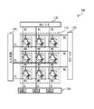
- FIG. 2 shows an example of the configuration of the product-sum calculation device 100.
- the product-sum calculation device 100 includes a product-sum calculation circuit 110 configured by connecting a plurality of cell MCs corresponding to synapses in a matrix, a row decoder 120, a column decoder 130, an input circuit 140, and an output circuit 150. And have.
- the product-sum calculation circuit 110 is driven by the row decoder 120, the column decoder 130, and the input circuit 140.
- the product-sum calculation circuit 110 is formed on, for example, a silicon substrate.
- a plurality of word line WLs are connected to the row decoder 120.
- a plurality of word lines WL are assigned to a plurality of cell MCs arranged in a matrix, for example, one for each row.
- a plurality of bit lines BL are connected to the column decoder 130.
- a plurality of bit lines BL are assigned to a plurality of cell MCs arranged in a matrix, for example, one for each column.
- a plurality of input wiring PLs are connected to the input circuit 140.
- a plurality of input wiring PLs are assigned to a plurality of cell MCs arranged in a matrix, for example, one for each row.
- a plurality of output wiring SLs are connected to each bit line BL one by one.
- the bit line BL and the output wiring SL are configured to be capable of accumulating a charge amount corresponding to the multiplication of the capacitance of the ferroelectric capacitor Cs of each cell MC and the input voltage input to the input wiring PL
- the row decoder 120 selects the cell MC to be accessed by applying a selection signal to the word line WL.
- the selection signal is a pulse having a peak value equal to or higher than the threshold voltage of the transistor Tr (described later) in the cell MC.
- the transistor Tr is turned on.
- the column decoder 130 supplies a predetermined voltage Vbl to each cell MC connected to the bit line BL by applying a predetermined voltage Vbl to the bit line BL.
- the input circuit 140 supplies a predetermined voltage (input voltage Vpl) to each cell MC connected to the input wiring PL by applying a predetermined voltage (input voltage Vpl) to the input wiring PL.
- a voltage difference between the input voltage Vpl applied to the input wiring PL and the voltage Vbl applied to the bit line BL is applied to each cell MC.
- the voltage Vbl is, for example, the ground voltage (0V) when the input voltage Vpl is a predetermined positive voltage. At this time, for example, "0" is stored in the cell MC as the polarization state of the cell MC. Further, when the input voltage Vpl is the ground voltage (0V), it is assumed that the voltage Vbl is a predetermined positive voltage. At this time, for example, "1" is stored in the cell MC as the polarization state of the cell MC.
- the input voltage Vpl is applied to the cell MC from the input circuit 140 through the input wiring PL, and the voltage Vbl is applied from the column decoder 130 through the bit line BL.
- a switching current corresponding to the polarization of the ferroelectric substance of the cell MC flows through the cell MC.
- Each output of the cell MC is connected to the output wiring SL via the bit line BL, and the output circuit 150 measures the current flowing through the output wiring SL or the potential of the output wiring SL to add up the products. Get the calculation result.
- the output circuit 150 has, for example, an AD (Analog-to-Digital) conversion circuit that measures each of the voltages of the output wiring SL simultaneously and in parallel, and is a digital obtained by AD-converting the product-sum calculation result. Output the signal to the outside.
- the output circuit 150 may further include an amplifier circuit or the like, if necessary.
- the product-sum calculation circuit 110 has a plurality of cell MCs arranged in a matrix.
- Each cell MC has a circuit configuration of 1Tr1C including, for example, a transistor Tr and a ferroelectric capacitor Cs connected to a source / drain terminal of the transistor Tr.
- the transistor Tr is, for example, a MOSFET.
- the ferroelectric capacitor Cs has a structure in which a ferroelectric material is sandwiched between a pair of electrodes. Examples of the ferroelectric material include hafnium oxide (HfOx), zirconium oxide (ZrOx), and hafnium oxide zirconium (HfZrOx).
- these materials can be made into a ferroelectric substance by performing crystallization annealing on hafnium oxide (HfOx), zirconium oxide (ZrOx), zirconium oxide (HfZrOx) and the like.
- the ferroelectric material may be doped with atoms such as La, Si, and Gd.
- titanium nitride (TiN), tantalum nitride (TaN), or the like can be used.
- the gate of the transistor Tr is connected to the word line WL, and a signal from the row decoder 120 is input via the word line WL.
- One source / drain terminal of the transistor Tr is connected to the input wiring PL via the ferroelectric capacitor Cs.
- One terminal of the ferroelectric capacitor Cs is connected to one source / drain terminal of the transistor Tr, and the other terminal of the ferroelectric capacitor Cs is connected to the input wiring PL.
- a signal from the input circuit 140 is input to one of the source / drain terminals of the transistor Tr via the ferroelectric capacitor Cs.
- a bit line BL is connected to the other source / drain terminal of the transistor Tr, and a signal from the column decoder 130 is input via the bit line BL.
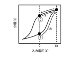
- C is, for example, as shown in FIG. 3, a load capacity cl corresponding to the polarization state (“0”) of the cell MC, or a load capacity corresponding to the polarization state (“1”) of the cell MC.
- C corresponds to ch. That is, in the product-sum calculation circuit 110, it is possible to perform a "product" between an input (for example, a signal in the previous stage) and a parameter in a neural network represented by a Convolution Neural Network (CNN).
- CNN Convolution Neural Network
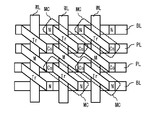
- FIG. 4 shows an example of the planar layout of the product-sum calculation circuit 110.
- the plurality of bit lines BL and the plurality of input wiring PL both have wiring extending in the first direction, and the wirings are alternately arranged in the second direction orthogonal to the first direction. ..
- the two input wiring PLs adjacent to each other are connected to each other by the conductive layer M, and correspond to the one input wiring PL of FIG. 2 above.
- a plurality of word lines WL extend in the second direction and are arranged in the first direction at predetermined intervals.
- the bit contact N is connected to the bit wire BL and one of the source / drain terminals of the transistor Tr.
- the bit contact N is arranged at a position where the bit wire BL and one of the source / drain terminals of the transistor Tr face each other.
- Ferroelectric capacitors Cs are provided between the other source / drain terminal of the transistor Tr and the input wiring PL.
- the ferroelectric capacitors Cs are arranged at positions where the input wiring PL and the other source / drain terminals of the transistor Tr face each other.
- a plurality of bit contacts N and a plurality of ferroelectric capacitors Cs are alternately arranged in the first direction.
- the transistor Tr is formed so as to extend in a third direction connecting the bit contact N and the ferroelectric capacitor Cs, and in the transistor Tr, one source / drain terminal and the other source / drain terminal are third. They are arranged so as to face each other in the direction of.
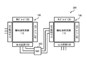
- FIG. 5 shows an example of the configuration of the neural network 200 using the two multiply-accumulate arithmetic units 100.
- the neural network 200 performs DA (Digital-to-Analog) conversion of a plurality of digital signals output from the two product-sum calculation devices 100 and the output circuit 150 of the product-sum calculation device 100 in the previous stage, and performs the product-sum calculation in the latter stage. It is provided with a DAC 300 for inputting to the input circuit 140 of the device 100. In this way, a neural network can be constructed by connecting the two multiply-accumulate arithmetic units 100 via the DAC 300. It is also possible to construct a neural network using a plurality of product-sum calculation devices 100. At this time, a DAC 300 is provided between the product-sum calculation device 100 on the front stage side and the product-sum calculation device 100 on the rear stage side.
- DA Digital-to-Analog
- the row decoder 120 selects a specific word line WL
- the input circuit 140 applies a positive voltage as the input voltage Vpl to the specific input wiring PL
- the column decoder 130 applies a specific bit line BL.
- a ground voltage is applied as the voltage Vbl
- it is connected to the selected word line WL
- the bit line BL to which the ground voltage is applied as the voltage Vbl.
- a voltage corresponding to the accumulated electric charge is generated in the output wiring SL, and the voltage of the output wiring SL is AD-converted in the output circuit 150 and output to the outside.
- a voltage corresponding to the sum of the charges supplied from each cell MC sharing the output wiring SL is generated in the output wiring SL, the voltage of the output wiring SL is AD converted in the output circuit 150, and the voltage is AD-converted from the output circuit 150. It is output to the outside.
- a voltage (product-sum calculation result) corresponding to the sum of the charges supplied from each cell MC sharing the output wiring SL is output from the output circuit 150 to the output wiring SL. It is output to the outside every time.
- the cell MC is provided with ferroelectric capacitors Cs. This makes it possible to hold parameters (weights) in the ferroelectric capacitors Cs.
- the variation of the load capacities cl and ch is large, the variation becomes noise at the time of inference, and there is a possibility that the inference accuracy is lowered.
- the variation of the load capacities cl and ch in the ferroelectric capacitor Cs that holds the parameter (weight) is small, high-precision inference can be performed.
- the cell MC of 1T1C using the ferroelectric capacitors Cs can be formed on the silicon substrate in a smaller area than the product-sum calculation cell using another memory (for example, ReRAM). Therefore, it is possible to provide a low-cost product-sum calculation device 100. Further, in the ferroelectric capacitor Cs, the upper limit of the number of rewrites is extremely large as compared with the case where another memory (for example, ReRAM) is used, and practically, the number of rewrites is not limited.
- an output circuit 150 is provided that AD-converts and outputs a voltage corresponding to the electric charge stored in each output wiring PL.
- an ADC is provided between the product-sum calculation device 100 on the front stage side and the product-sum calculation device 100 on the rear stage side, thereby providing a neural network. It is possible to build.
- each transistor Tr extends in an oblique direction intersecting both the row direction and the column direction in the plurality of cell MCs, and in each transistor Tr, the pair of source / drain terminals are in the oblique direction. They are arranged facing each other.
- the product-sum calculation circuit 110 can be formed in a square shape on the surface of the semiconductor substrate, and the degree of freedom in design can be improved.
- the input wiring PL is arranged at a position facing one source / drain terminal via the ferroelectric capacitor Cs, and the output wiring SL is arranged at a position facing the other source / drain terminal.
- the product-sum calculation circuit 110 can be formed in a square shape on the surface of the semiconductor substrate, and the degree of freedom in design can be improved.
- FIG. 6 shows an example of the configuration of the product-sum calculation device 400.
- the product-sum calculation device 400 includes a product-sum calculation circuit 410 composed of a plurality of cells MCd corresponding to synapses connected in a matrix, a row decoder 420, a column decoder 430, an input circuit 440, and an output circuit 450. And have.
- the product-sum calculation circuit 410 is driven by the row decoder 420, the column decoder 430, and the input circuit 440.
- the product-sum calculation circuit 410 is formed on, for example, a silicon substrate.
- a plurality of word lines WL + and WL- are connected to the row decoder 420.
- a plurality of word lines WL + are assigned to a plurality of cells MCd arranged in a matrix, for example, one line for each row.
- a plurality of bit lines BL + and BL ⁇ are connected to the column decoder 430.
- a plurality of bit lines BL + are assigned to a plurality of cells MCd arranged in a matrix, for example, one for each column.
- a plurality of input wiring PLs are connected to the input circuit 440.
- a plurality of input wiring PLs are assigned to a plurality of cells MCd arranged in a matrix, for example, one for each row.
- a plurality of output wiring SL + are connected to each bit line BL + one by one.
- a plurality of output wiring SL-s are connected to each bit line BL-.
- the bit line BL- and the output wiring SL- are configured to be capable of accumulating a charge amount corresponding to the multiplication of the capacitance of the ferroelectric capacitor Cs1 of each cell MC1 and the input voltage input to the input wiring PL.
- the product-sum calculation circuit 410 has a plurality of cells MCd arranged in a matrix. As shown in FIG. 7, each cell MCd has, for example, a circuit configuration of 2Tr2C including two cell MCs (cells MC1 and MC2). In each cell MCd, the cell MC1 is the main cell and the cell MC2 is the reference cell. When a predetermined state is set for the cell MC1, a state in which the state of the cell MC1 is inverted is set for the cell MC2. The role of the reference cell will be described in detail later.
- the cells MC1 and MC2 have the same configuration and function as the cell MC according to the above embodiment.
- the cell MC1 has a circuit configuration of 1Tr1C including, for example, a transistor Tr1 and a ferroelectric capacitor Cs1 connected to a source / drain terminal of the transistor Tr1.
- the cell MC2 has a circuit configuration of 1Tr1C including, for example, a transistor Tr2 and a ferroelectric capacitor Cs2 connected to a source / drain terminal of the transistor Tr2.
- the transistors Tr1 and Tr2 are, for example, MOSFETs.
- the ferroelectric capacitors Cs1 and Cs2 have a structure in which a ferroelectric material is sandwiched between a pair of electrodes.
- the gate of the transistor Tr1 is connected to the word line WL-, and a signal from the row decoder 420 is input via the word line WL-.
- One source / drain terminal of the transistor Tr1 is connected to the input wiring PL via the ferroelectric capacitor Cs1.
- One terminal of the ferroelectric capacitor Cs1 is connected to one source / drain terminal of the transistor Tr1, and the other terminal of the ferroelectric capacitor Cs1 is connected to the input wiring PL.
- a signal from the input circuit 440 is input to one of the source / drain terminals of the transistor Tr1 via the ferroelectric capacitor Cs1.
- a bit line BL- is connected to the other source / drain terminal of the transistor Tr1, and a signal from the column decoder 430 is input via the bit line BL-.
- the gate of the transistor Tr2 is connected to the word line WL +, and a signal from the row decoder 420 is input via the word line WL +.
- One source / drain terminal of the transistor Tr2 is connected to the input wiring PL to which the ferroelectric capacitor Cs1 is connected via the ferroelectric capacitor Cs2.
- One terminal of the ferroelectric capacitor Cs2 is connected to one source / drain terminal of the transistor Tr2, and the other terminal of the ferroelectric capacitor Cs2 is connected to the input wiring PL to which the ferroelectric capacitor Cs1 is connected. .. That is, in the cell MCd, the ferroelectric capacitors Cs1 and Cs2 are connected to the common input wiring PL.
- a signal from the input circuit 440 is input to one of the source / drain terminals of the transistor Tr2 via the ferroelectric capacitor Cs2.
- a bit line BL + is connected to the other source / drain terminal of the transistor Tr2, and a signal from the column decoder 430 is input via the bit line BL +.
- the row decoder 420 selects the cell MCd (or cell MC1) to be accessed by applying the selection signal to the word line WL-.
- the selection signal is a pulse having a peak value equal to or higher than the threshold voltage of the transistor Tr1.
- the transistor Tr1 is turned on.
- the column decoder 430 supplies a predetermined voltage Vbl1 to each cell MC1 connected to the bit line BL- by applying a predetermined voltage Vbl1 to the bit line BL-. A voltage difference between the input voltage Vpl applied to the input wiring PL and the voltage Vbl1 applied to the bit line BL- is applied to each cell MC1.
- the row decoder 420 selects the cell MCd (or cell MC2) to be accessed by applying the selection signal to the word line WL +.
- the selection signal is a pulse having a peak value equal to or higher than the threshold voltage of the transistor Tr2.
- the transistor Tr2 is turned on.
- the column decoder 430 supplies a predetermined voltage Vbl2 to each cell MC2 connected to the bit line BL + by applying a predetermined voltage Vbl2 to the bit line BL +.
- a voltage difference between the input voltage Vpl applied to the input wiring PL and the voltage Vbl2 applied to the bit line BL + is applied to each cell MC2.
- the voltage Vbl1 is, for example, the ground voltage (0V) when the input voltage Vpl is a predetermined positive voltage. At this time, for example, "0" is stored in the cell MC1 as the polarization state of the cell MC1. Further, it is assumed that the voltage Vbl1 is a predetermined positive voltage when the input voltage Vpl is the ground voltage (0V). At this time, for example, "1" is stored in the cell MC1 as the polarization state of the cell MC1.
- the voltage Vbl2 is, for example, the ground voltage (0V) when the input voltage Vpl is a predetermined positive voltage. At this time, for example, "0" is stored in the cell MC2 as the polarization state of the cell MC2. Further, it is assumed that the voltage Vbl2 is a predetermined positive voltage when the input voltage Vpl is the ground voltage (0V). At this time, for example, "1" is stored in the cell MC2 as the polarization state of the cell MC2.
- the input voltage Vpl is applied to the cell MC1 from the input circuit 440 through the input wiring PL, and the voltage Vbl1 is applied from the column decoder 430 through the bit line BL-.
- a switching current corresponding to the polarization of the ferroelectric substance of the cell MC1 flows through the cell MC1.
- Each output of the cell MC1 is connected to the output wiring SL- via the bit line BL-, and the output circuit 450 measures the current flowing through the output wiring SL- or the potential of the output wiring SL-. To get the product-sum operation result.
- the output circuit 450 has, for example, an AD conversion circuit that simultaneously and in parallel measures each of the voltages of the output wiring SL-, and outputs a digital signal obtained by AD conversion of the product-sum calculation result to the outside. ..
- the output circuit 450 may further include an amplifier circuit or the like, if necessary.
- C is, for example, as shown in FIG. 3, a load capacity cl corresponding to the polarization state (“0”) of the cell MC1, or a load capacity corresponding to the polarization state (“1”) of the cell MC1.
- C corresponds to ch. That is, in the product-sum calculation circuit 110, it is possible to perform a "product" between an input (for example, a signal in the previous stage) and a parameter in a neural network represented by a Convolution Neural Network (CNN).
- CNN Convolution Neural Network
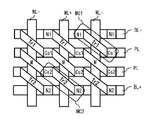
- FIG. 8 shows an example of the planar layout of the product-sum calculation circuit 410.
- a plurality of bit lines BL-, BL + and a plurality of input wiring PLs have wiring extending in the first direction, and the wirings are in the second direction orthogonal to the first direction, the bit line BL.
- the two input wiring PL and the bit line BL + are repeatedly arranged in this order.
- the two input wiring PLs adjacent to each other are connected to each other by the conductive layer M, and correspond to the one input wiring PL of FIG. 7 above.
- a plurality of word lines WL + and WL- extend in the second direction and are alternately arranged in the first direction.
- the bit contact N1 is connected to the bit wire BL- and one of the source / drain terminals of the transistor Tr1.
- the bit contact N1 is arranged at a position where the bit wire BL- and one source / drain terminal of the transistor Tr1 face each other.
- a ferroelectric capacitor Cs1 is provided between the other source / drain terminal of the transistor Tr1 and the input wiring PL.
- the ferroelectric capacitor Cs1 is arranged at a position where the input wiring PL and the other source / drain terminal of the transistor Tr face each other.
- the bit contact N2 is connected to the bit line BL + and one of the source / drain terminals of the transistor Tr2.
- the bit contact N2 is arranged at a position where the bit line BL + and one of the source / drain terminals of the transistor Tr2 face each other.
- a ferroelectric capacitor Cs2 is provided between the other source / drain terminal of the transistor Tr2 and the input wiring PL.
- the ferroelectric capacitor Cs2 is arranged at a position where the input wiring PL and the other source / drain terminal of the transistor Tr2 face each other.
- a plurality of bit contacts N1 and N2 and a plurality of ferroelectric capacitors Cs1 and Cs2 are repeatedly arranged in the first direction in the order of the bit contact N1, the ferroelectric capacitor Cs1, the ferroelectric capacitor Cs2, and the bit contact N2.
- the transistor Tr1 is formed so as to extend in a third direction intersecting the first direction and the second direction, and in the transistor Tr1, one source / drain terminal and the other source / drain terminal are the first. They are arranged so as to face each other in the direction of 3.
- the transistor Tr2 is formed so as to extend in a first direction and a third direction intersecting the second direction, and in the transistor Tr2, one source / drain terminal and the other source / drain terminal are the first. They are arranged so as to face each other in the direction of 3.
- FIG. 9 shows an example of the configuration of the neural network 500 using the two multiply-accumulate arithmetic units 400.
- the neural network 500 performs DA (Digital-to-Analog) conversion of a plurality of digital signals output from the two product-sum calculation devices 400 and the output circuit 450 of the product-sum calculation device 400 in the previous stage, and performs the product-sum calculation in the latter stage.
- DA Digital-to-Analog
- DAC 600 Digital-to-Analog
- a DAC 600 to be input to the input circuit 440 of the device 400.
- a neural network can be constructed by connecting the two multiply-accumulate arithmetic units 400 via the DAC 600.
- a DAC 600 is provided between the product-sum calculation device 400 on the front stage side and the product-sum calculation device 400 on the rear stage side.
- the row decoder 420 selects a specific word line WL-, the input circuit 140 applies a positive voltage as the input voltage Vpl to the specific input wiring PL, and the column decoder 130 applies a specific bit line.
- a ground voltage is applied to BL- as a voltage Vbl
- the selected word line WL- an input wiring PL to which a positive voltage is applied as an input voltage Vpl
- a bit line BL- to which a ground voltage is applied as a voltage Vbl.
- a voltage corresponding to the accumulated electric charge is generated in the output wiring SL-, and the voltage of the output wiring SL- is AD converted in the output circuit 450 and output to the outside.
- a voltage corresponding to the sum of the charges supplied from each cell MC1 sharing the output wiring SL- is generated in the output wiring SL-, and the voltage of this output wiring SL- is AD converted in the output circuit 450 and output. It is output to the outside from the circuit 450.
- a voltage (product-sum calculation result) corresponding to the sum of the charges supplied from each cell MC1 sharing the output wiring SL- is output from the output circuit 450. It is output to the outside for each wiring SL-.
- the product-sum calculation circuit 110 gives the cell MC2, which is a reference cell, a function of backing up the cell MC1.
- the product-sum calculation circuit 110 for example, writes "1" as a state in the cell MC1, writes a state "0" in which the state of the cell MC1 is inverted, in the cell MC2, and then infers the product-sum calculation.
- the cell MC1 becomes “0”.
- the product-sum calculation device 400 writes in the cell MC1 a state (“1”) in which the state (“0”) read from the cell MC2 is inverted. In this way, rewriting to the cell MC1 is performed. Such rewriting can be realized by making the cell MC2 function as a backup of the cell MC1.
- the cell MC is provided with the ferroelectric capacitors Cs1 and Cs2. This makes it possible to hold parameters (weights) in the ferroelectric capacitors Cs1 and Cs2.
- the variation of the load capacities cl and ch is large, the variation becomes noise at the time of inference, and there is a possibility that the inference accuracy is lowered.
- the variation of the load capacities cl and ch in the ferroelectric capacitors Cs1 and Cs2 that hold the parameters (weights) is small, high-precision inference can be performed.
- the 1T1C cell MC1 using the ferroelectric capacitor Cs1 and the 1T1C cell MC2 using the ferroelectric capacitor Cs2 have a smaller area than the product-sum operation cell using another memory (for example, ReRAM). It can be formed on a silicon substrate. Therefore, it is possible to provide a low-cost product-sum calculation device 100. Further, in the ferroelectric capacitors Cs1 and Cs2, the upper limit of the number of rewrites is extremely large as compared with the case where other memories (for example, ReRAM) are used, and practically, the number of rewrites is not limited.
- an output circuit 450 is provided that AD-converts and outputs a voltage corresponding to the electric charge stored in each output wiring PL-.
- an ADC is provided between the product-sum calculation device 400 on the front stage side and the product-sum calculation device 400 on the rear stage side, thereby providing a neural network. It is possible to build.
- each transistor Tr1 and Tr2 extends in an oblique direction intersecting both the row direction and the column direction in the plurality of cells MCd, and each transistor Tr1 and Tr2 has a pair of source / drain terminals. Are arranged so as to face each other in the diagonal direction.
- the product-sum calculation circuit 410 can be formed in a square shape on the surface of the semiconductor substrate, and the degree of freedom in design can be improved.
- the input wiring PL is arranged at a position facing one source / drain terminal via the ferroelectric capacitors Cs1 and Cs2, and the output wiring SL- faces the other source / drain terminal. It is placed in a position.
- the product-sum calculation circuit 410 can be formed in a square shape on the surface of the semiconductor substrate, and the degree of freedom in design can be improved.
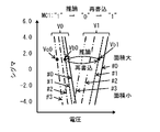
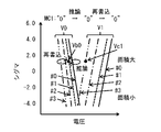
- 11 and 12 show an example of the distribution of the voltage V0 at “0” and the voltage V1 at “1” read from each cell MC in the 64-kbit cell array.
- 11 and 12 illustrate the distribution of voltages V0 and V1 when the areas of the ferroelectric capacitors Cs1 included in the cell MC1 are # 0, # 1, # 2, and # 3.
- the voltage V1 when "1" is held in the cell MC1 having the area # 1 is Vb1
- the voltage V0 when "0” is held in the cell MC1 having the area # 1 is Vb0.
- Vc1 be the voltage V1 when "1" is held in the cell MC1 having the area # 3
- Vc0 be the voltage V0 when "0" is held in the cell MC1 having the area # 3.
- the product-sum operation when the area of the cell MC1 is # 1 and the area of the cell MC2 is # 3 will be described below.
- the control device that controls the product-sum calculation device 400 writes “1" in the cell MC1 and writes "0" in the cell MC2, and then infers the product-sum calculation. At this time, since the inference of the product-sum operation is a destructive read, the cell MC1 becomes “0” (FIG. 11). Subsequently, the control device that controls the product-sum calculation device 400 reads "0" from the cell MC1 and "0” from the cell MC2, and obtains the voltage Vb0 obtained from the cell MC1 and the voltage Vb0 obtained from the cell MC2. When it is confirmed that Vb0> Vc0 by comparing with the voltage Vc0, "1" is written in the cell MC1 (FIG. 11). In this way, rewriting to the cell MC1 is performed. Such rewriting can be realized by making the cell MC2 function as a backup of the cell MC1.
- the control device that controls the product-sum calculation device 400 writes “0" in the cell MC1 and writes “1” in the cell MC2, and then infers the product-sum calculation. At this time, the cell MC1 remains “0” (FIG. 12). Subsequently, the control device that controls the product-sum calculation device 400 reads "0" from the cell MC1 and "1” from the cell MC2, and obtains the voltage Vb0 obtained from the cell MC1 and the voltage Vb0 obtained from the cell MC2. When it is confirmed that Vb0 ⁇ Vc1 by comparing with the voltage Vc1, "0" is written in the cell MC1 (FIG. 12). In this way, rewriting to the cell MC1 is performed. Such rewriting can be realized by making the cell MC2 function as a backup of the cell MC1.
- the bit line BL itself may also serve as the output wiring PL.
- the plurality of input wiring PLs may be assigned one by one for each row in the plurality of cell MCs, or may be assigned by two. .. Further, in the second embodiment and the modified examples thereof, one plurality of input wirings may be assigned to each row in the plurality of cell MCs, or two wiring wirings may be assigned to each row. ..
- the present disclosure may have the following structure.
- (1) A plurality of cells arranged in a matrix, each including a transistor and a ferroelectric capacitor connected to a first source / drain terminal of the transistor.
- a plurality of input wires assigned to each row in the plurality of cells and connected to the ferroelectric capacitor, and a plurality of input wires. Allocated one for each column in the plurality of cells, connected to the second source / drain terminal of the transistor, and multiplied by the capacitance of the dielectric capacitor in each cell and the input voltage input to the input wiring.
- the product-sum calculation device further comprising an output circuit that AD-converts and outputs a voltage corresponding to the electric charge accumulated in each output wiring.
- Each of the transistors extends in an oblique direction intersecting both the row and column directions in the plurality of cells.
- the product-sum calculation device according to (1) or (2), wherein in each of the transistors, the first source / drain terminal and the second source / drain terminal are arranged so as to face each other in the diagonal direction.
- the input wiring is arranged at a position facing the first source / drain terminal via the ferroelectric capacitor.
- the product-sum calculation device wherein the output wiring is arranged at a position facing the second source / drain terminal.
- a main cell each containing a first transistor and a first dielectric capacitor connected to a first source / drain terminal of the first transistor, a second transistor, and a second transistor, respectively.
- a plurality of cells arranged in a matrix including a reference cell including a second dielectric capacitor connected to a second source / drain terminal of the transistor, and a plurality of cells.
- a plurality of input wires allocated to each row in the plurality of cells and connected to the first ferroelectric capacitor and the second ferroelectric capacitor.
- One is assigned to each column in the plurality of cells, connected to the third source / drain terminal of the first transistor, and to the capacitance of the first dielectric capacitor and the input wiring of each main cell.
- a plurality of first output wires capable of accumulating the amount of charge corresponding to the multiplication of the input input voltage, and One is assigned to each row in the plurality of cells, connected to the fourth source / drain terminal of the second transistor, and to the capacity of the second dielectric capacitor and the input wiring of each reference cell.
- Each said first transistor and each said second transistor extends in an oblique direction intersecting both the row and column directions in the plurality of cells.
- the first source / drain terminal and the third source / drain terminal are arranged so as to face each other in the diagonal direction.
- Device Two of the plurality of input wires are assigned to each row in the plurality of cells.
- the first input wiring is arranged at a position facing the first source / drain terminal via the first strong dielectric capacitor.
- Each of the product-sum calculation devices A plurality of cells arranged in a matrix, each including a transistor and a ferroelectric capacitor connected to a first source / drain terminal of the transistor.
- Each of the product-sum calculation devices A main cell, each containing a first transistor and a first dielectric capacitor connected to a first source / drain terminal of the first transistor, a second transistor, and a second transistor, respectively.
- a plurality of cells arranged in a matrix including a reference cell including a second dielectric capacitor connected to a second source / drain terminal of the transistor, and a plurality of cells.
- One is assigned to each row in the plurality of cells, connected to the third source / drain terminal of the first transistor, and to the capacitance of the first dielectric capacitor and the input wiring of each main cell.
- a plurality of first output wires capable of accumulating the amount of charge corresponding to the multiplication of the input input voltage, and One is assigned to each row in the plurality of cells, connected to the fourth source / drain terminal of the second transistor, and to the capacity of the second dielectric capacitor and the input wiring of each reference cell.
- a ferroelectric capacitor is provided in the cell. This makes it possible to hold parameters (weights) in the ferroelectric capacitor.
- the variation in the load capacity of the cell is large, the variation becomes noise at the time of inference, and there is a possibility that the inference accuracy is lowered.
- the variation in the load capacitance in the ferroelectric capacitor that holds the parameter (weight) is small, high-precision inference can be performed.
- the upper limit of the number of rewrites is extremely large as compared with the case where another memory (for example, ReRAM) is used, and practically, the number of rewrites is not limited. Therefore, it is possible to provide a product-sum calculation device capable of holding parameters and performing writing a number of times to withstand practical use.
- a ferroelectric capacitor is provided in the first cell and the second cell. This makes it possible to hold parameters (weights) in the ferroelectric capacitor.
- the variation in the load capacity of the cell is large, the variation becomes noise at the time of inference, and there is a possibility that the inference accuracy is lowered.
- the variation in the load capacitance in the ferroelectric capacitor that holds the parameter (weight) is small, high-precision inference can be performed.
- the upper limit of the number of rewrites is extremely large as compared with the case where another memory (for example, ReRAM) is used, and practically, the number of rewrites is not limited. Therefore, it is possible to provide a product-sum calculation device capable of holding parameters and performing writing a number of times to withstand practical use.
Landscapes
- Engineering & Computer Science (AREA)
- Physics & Mathematics (AREA)
- Theoretical Computer Science (AREA)
- Biomedical Technology (AREA)
- Life Sciences & Earth Sciences (AREA)
- Health & Medical Sciences (AREA)
- General Physics & Mathematics (AREA)
- General Health & Medical Sciences (AREA)
- Molecular Biology (AREA)
- Neurology (AREA)
- Computer Hardware Design (AREA)
- Biophysics (AREA)
- Computing Systems (AREA)
- General Engineering & Computer Science (AREA)
- Computational Linguistics (AREA)
- Evolutionary Computation (AREA)
- Data Mining & Analysis (AREA)
- Artificial Intelligence (AREA)
- Mathematical Physics (AREA)
- Software Systems (AREA)
- Power Engineering (AREA)
- Computational Mathematics (AREA)
- Mathematical Analysis (AREA)
- Mathematical Optimization (AREA)
- Pure & Applied Mathematics (AREA)
- Semiconductor Memories (AREA)
Abstract
本開示の一側面に係る積和演算装置は、各々がトランジスタと、トランジスタの第1のソース・ドレイン端子に接続された強誘電キャパシタとを含み、行列状に配置された複数のセルを備えている。この積和演算装置は、さらに、複数の入力配線と、複数の出力配線とを備えている。複数の入力配線は、複数のセルにおける行ごとに1もしくは複数本ずつ割り当てられ、強誘電キャパシタに接続されている。複数の出力配線は、複数のセルにおける列ごとに1本ずつ割り当てられている。複数の出力配線は、トランジスタの第2のソース・ドレイン端子に接続され、各セルの強誘電キャパシタの容量および入力配線へ入力される入力電圧の乗算に対応する電荷量を蓄積可能に構成されている。
Description
本開示は、強誘電キャパシタを用いた積和演算装置およびニューラルネットワークに関する。
近年、画像やパターンの認証を行う応用としてニューラルネットワーク回路が実用されている。メモリアレイをニューラルネットワーク回路の積和演算として利用することで、ノイマン型コンピューティングの課題であるメモリとCPU間の遅延や消費電力を解決することが期待できる。積和演算の例として、例えば、特許文献1~3に記載の方法が挙げられる。
ところで、上記特許文献1,2に記載の発明では、揮発性の容量結合メモリにパラメータ(重み)が記憶されるため、パラメータを保持することができない。また、上記特許文献3に記載の発明では、強誘電トランジスタにパラメータが記憶されるため、書き込み回数(パラメータの書き換え回数)に実用に耐えない制限がある。従って、パラメータを保持することができ、かつ実用に耐える程度の回数の書き込みを行うことの可能な積和演算装置およびニューラルネットワークを提供することが望ましい。
本開示の第1の側面に係る積和演算装置は、各々がトランジスタと、トランジスタの第1のソース・ドレイン端子に接続された強誘電キャパシタとを含み、行列状に配置された複数のセルを備えている。この積和演算装置は、さらに、複数の入力配線と、複数の出力配線とを備えている。複数の入力配線は、複数のセルにおける行ごとに1もしくは複数本ずつ割り当てられ、強誘電キャパシタに接続されている。複数の出力配線は、複数のセルにおける列ごとに1本ずつ割り当てられている。複数の出力配線は、トランジスタの第2のソース・ドレイン端子に接続され、各セルの強誘電キャパシタの容量および入力配線へ入力される入力電圧の乗算に対応する電荷量を蓄積可能に構成されている。
本開示の第2の側面に係るニューラルネットワークは、複数の積和演算装置を備えている。各積和演算装置は、上記の第1の側面に係る積和演算装置と同様の構成要素を備えている。
本開示の第1の側面に係る積和演算装置、および本開示の第2の側面に係るニューラルネットワークでは、セルには強誘電キャパシタが設けられている。これにより、強誘電キャパシタにパラメータ(重み)を保持することが可能となる。ここで、セルの負荷容量のばらつきが大きい場合、そのばらつきが推論の際のノイズとなり、推論精度の低下が生じる可能性がある。しかし、本開示では、パラメータ(重み)を保持させる強誘電キャパシタにおける負荷容量のばらつきは小さいので、高精度の推論を行うことができる。また、強誘電キャパシタでは、他のメモリ(例えば、ReRAM)を用いた場合と比べて、書き換え回数の上限が極めて大きく、実用上、書き換え回数の制限を受けない。
本開示の第3の側面に係る積和演算装置は、行列状に配置された複数のセルを備えている。各セルは、メインセルとレファレンスセルとを含む。メインセルは、第1のトランジスタと、第1のトランジスタの第1のソース・ドレイン端子に接続された第1の強誘電キャパシタとを含む。レファレンスセルは、第2のトランジスタと、第2のトランジスタの第2のソース・ドレイン端子に接続された第2の強誘電キャパシタとを含む。この積和演算装置は、さらに、複数の入力配線と、複数の第1の出力配線と、複数の第2の出力配線とを備えている。複数の入力配線は、複数のセルにおける行ごとに1もしくは複数本ずつ割り当てられ、第1の強誘電キャパシタおよび第2の強誘電キャパシタに接続されている。複数の第1の出力配線は、複数のセルにおける列ごとに1本ずつ割り当てられ、第1のトランジスタの第3のソース・ドレイン端子に接続され、各メインセルの第1の強誘電キャパシタの容量および入力配線へ入力される入力電圧の乗算に対応する電荷量を蓄積可能に構成されている。複数の第2の出力配線は、複数のセルにおける列ごとに1本ずつ割り当てられ、第2のトランジスタの第4のソース・ドレイン端子に接続され、各レファレンスセルの第2の強誘電キャパシタの容量および入力配線へ入力される入力電圧の乗算に対応する電荷量を蓄積可能に構成されている。
本開示の第4の側面に係るニューラルネットワークは、複数の積和演算装置を備えている。各積和演算装置は、上記の第3の側面に係る積和演算装置と同様の構成要素を備えている。
本開示の第3の側面に係る積和演算装置、および本開示の第4の側面に係るニューラルネットワークでは、第1のセルおよび第2のセルには強誘電キャパシタが設けられている。これにより、強誘電キャパシタにパラメータ(重み)を保持することが可能となる。ここで、セルの負荷容量のばらつきが大きい場合、そのばらつきが推論の際のノイズとなり、推論精度の低下が生じる可能性がある。しかし、本開示では、パラメータ(重み)を保持させる強誘電キャパシタにおける負荷容量のばらつきは小さいので、高精度の推論を行うことができる。また、強誘電キャパシタでは、他のメモリ(例えば、ReRAM)を用いた場合と比べて、書き換え回数の上限が極めて大きく、実用上、書き換え回数の制限を受けない。
以下、本開示を実施するための形態について、図面を参照して詳細に説明する。なお、本明細書および図面において、実質的に同一の機能構成を有する構成要素については、同一の符号を付することにより重複説明を省略する。
<1.本開示に係る技術的背景>
まず、図1を参照して、本開示に係る技術的背景について説明する。ニューラルネットワークは、生体の神経回路網をモデルとした情報処理システムである。ニューラルネットワークは、画像認識、又は画像の圧縮若しくは復元等のデジタル計算機では負荷が高い演算を効率良く実行することができる。このようなニューラルネットワークの1つとして、例えば、層状に並べられた人工ニューロンが隣接層間でのみ結合し、入力側から出力側に一方向にのみ情報が伝搬するパーセプトロンを例示することができる。
まず、図1を参照して、本開示に係る技術的背景について説明する。ニューラルネットワークは、生体の神経回路網をモデルとした情報処理システムである。ニューラルネットワークは、画像認識、又は画像の圧縮若しくは復元等のデジタル計算機では負荷が高い演算を効率良く実行することができる。このようなニューラルネットワークの1つとして、例えば、層状に並べられた人工ニューロンが隣接層間でのみ結合し、入力側から出力側に一方向にのみ情報が伝搬するパーセプトロンを例示することができる。
図1は、ニューラルネットワークの一例を表したものである。ニューラルネットワークは、例えば、入力層IL、中間層ML(隠れ層)および出力層OLを含む。各層(IL,ML,OL)は、1または複数のニューロンを備えている。例えば、入力層ILのニューロンの数は、例えば、動画データに含まれる画素数に応じて設定することができる。中間層MLのニューロンの数は、適宜設定することができる。出力層OLは、後段で必要となる数に応じて設定することができる。
互いに隣接する層のニューロン同士は結合されており、各結合には重み(結合荷重)が設定されている。ニューロンの結合数は、適宜設定されてよい。各ニューロンには閾値が設定されており、例えば、各ニューロンへの入力値と重みとの積の和が閾値を超えているか否かによって各ニューロンの出力値が決定される。
<2.第1の実施の形態>
次に、本開示の第1の実施の形態に係る積和演算装置100について説明する。図2は、積和演算装置100の構成の一例を表したものである。積和演算装置100は、シナプスに対応する複数のセルMCが行列状に接続されることにより構成される積和演算回路110と、行デコーダ120、列デコーダ130、入力回路140と、出力回路150とを備えている。行デコーダ120、列デコーダ130および入力回路140によって積和演算回路110が駆動される。積和演算回路110は、例えば、シリコン基板上に形成されている。
次に、本開示の第1の実施の形態に係る積和演算装置100について説明する。図2は、積和演算装置100の構成の一例を表したものである。積和演算装置100は、シナプスに対応する複数のセルMCが行列状に接続されることにより構成される積和演算回路110と、行デコーダ120、列デコーダ130、入力回路140と、出力回路150とを備えている。行デコーダ120、列デコーダ130および入力回路140によって積和演算回路110が駆動される。積和演算回路110は、例えば、シリコン基板上に形成されている。
行デコーダ120には複数のワード線WLが接続されている。複数のワード線WLは、行列状に配置された複数のセルMCに対して、例えば、行ごとに1本ずつ割り当てられている。列デコーダ130には複数のビット線BLが接続されている。複数のビット線BLは、行列状に配置された複数のセルMCに対して、例えば、列ごとに1本ずつ割り当てられている。入力回路140には複数の入力配線PLが接続されている。複数の入力配線PLは、行列状に配置された複数のセルMCに対して、例えば、行ごとに1本ずつ割り当てられている。各ビット線BLには、複数の出力配線SLが1本ずつ接続されている。ビット線BLおよび出力配線SLは、各セルMCの強誘電キャパシタCsの容量および入力配線PLへ入力される入力電圧の乗算に対応する電荷量を蓄積可能に構成されている。
行デコーダ120は、ワード線WLに選択信号を印可することにより、アクセス対象であるセルMCを選択する。選択信号は、セルMC内のトランジスタTr(後述)の閾値電圧以上の波高値を有するパルスである。行デコーダ120によって選択されたセルMCでは、トランジスタTrが導通状態(オン)となる。列デコーダ130は、ビット線BLに所定の電圧Vblを印可することにより、ビット線BLに接続された各セルMCに所定の電圧Vblを供給する。入力回路140は、入力配線PLに所定の電圧(入力電圧Vpl)を印可することにより、入力配線PLに接続された各セルMCに所定の電圧(入力電圧Vpl)を供給する。各セルMCには、入力配線PLに印加された入力電圧Vplと、ビット線BLに印加された電圧Vblとの差分の電圧が印可される。
ここで、入力電圧Vplが所定の正の電圧となっている場合に、電圧Vblが、例えば、グラウンド電圧(0V)となっているとする。このとき、セルMCには、セルMCの分極状態として例えば、“0”が記憶される。また、入力電圧Vplがグラウンド電圧(0V)となっている場合に、電圧Vblが所定の正の電圧となっているとする。このとき、セルMCには、セルMCの分極状態として例えば、“1”が記憶される。
セルMCには、入力回路140から入力配線PLを通じて入力電圧Vplが印加されるとともに、列デコーダ130からビット線BLを通じて電圧Vblが印可される。これにより、セルMCには、セルMCの強誘電体の分極に応じたスイッチング電流が流れる。セルMCの各々の出力は、ビット線BLを介して出力配線SLに接続されており、出力回路150は、出力配線SLに流れる電流、または、出力配線SLの電位を測定することで、積和演算結果を取得する。出力回路150は、例えば、出力配線SLの電圧の各々を同時かつ並列に測定するAD(Analog-to-Digital)変換回路を有しており、積和演算結果をAD変換することにより得られるデジタル信号を外部に出力する。なお、出力回路150は、必要に応じて、増幅回路などをさらに有していてもよい。
積和演算回路110は、行列状に配置された複数のセルMCを有している。各セルMCは、例えば、トランジスタTrと、トランジスタTrのソース・ドレイン端子に接続された強誘電キャパシタCsとを含んで構成された1Tr1Cの回路構成となっている。トランジスタTrは、例えば、MOSFETである。強誘電キャパシタCsは、一対の電極間に強誘電体材料が挟み込まれた構成となっている。強誘電体材料としては、例えば、酸化ハフニウム(HfOx)、酸化ジルコニウム(ZrOx)、酸化ハフニウムジルコニウム(HfZrOx)などが挙げられる。例えば、酸化ハフニウム(HfOx)、酸化ジルコニウム(ZrOx)、酸化ハフニウムジルコニウム(HfZrOx)などに対して結晶化アニールを行うことにより、これらの材料を強誘電体にすることが可能である。強誘電体材料には、La,Si,Gd等の原子がドープされていてもよい。強誘電キャパシタCsの電極には、例えば、窒化チタン(TiN)や窒化タンタル(TaN)等が用いられ得る。
トランジスタTrのゲートはワード線WLに接続されており、ワード線WLを介して行デコーダ120からの信号が入力される。トランジスタTrの一方のソース・ドレイン端子は強誘電キャパシタCsを介して入力配線PLに接続されている。強誘電キャパシタCsの一方の端子がトランジスタTrの一方のソース・ドレイン端子に接続されており、強誘電キャパシタCsの他方の端子が入力配線PLに接続されている。トランジスタTrの一方のソース・ドレイン端子には強誘電キャパシタCsを介して入力回路140からの信号が入力される。トランジスタTrの他方のソース・ドレイン端子にはビット線BLが接続されており、ビット線BLを介して列デコーダ130からの信号が入力される。
積和演算回路110では、例えば、行デコーダ120によって選択されたセルMCの入力(入力配線PL)に電圧(入力電圧Vpl)が印可されると、強誘電キャパシタCsの容量と、入力電圧Vplとの乗算に対応する電荷量が出力配線SLに蓄積され、これにより積和演算を行うことができる。例えば、積和演算の推論においては、行デコーダ120によって選択されたセルMCの入力(入力配線PL)に電圧(入力電圧Vpl)が印可されると、C×V=Qに応じた電荷量が出力配線SLに蓄積される。ここで、Cは、例えば、図3に示したように、セルMCの分極状態(“0”)に応じた負荷容量cl、または、セルMCの分極状態(“1”)に応じた負荷容量chに対応する。すなわち、積和演算回路110において、Convolution Neural Network(CNN)に代表されるニューラルネットワークにおける入力(例えば、前段の信号)とパラメータとの“積” を行うことができる。
なお、強誘電キャパシタCsの分極状態が“1”のときにキャパシタCsに印加される電圧が0(V)→Va(V)→0(V)と変化すると、キャパシタCsの分極状態が“0”となる。また、強誘電キャパシタCsの分極状態が“0”のときにキャパシタCsに印加される電圧が0(V)→Va(V)→0(V)と変化すると、キャパシタCsの分極状態は、遷移前と同じ状態“0”となる。従って、積和演算回路110では、データ読み出しの際に、セルMCに保持されたデータが破壊される場合がある。
図4は、積和演算回路110の平面レイアウトの一例を表したものである。複数のビット線BLおよび複数の入力配線PLがともに第1の方向に延在する配線を有しており、それらの配線が第1の方向と直交する第2の方向に交互に配置されている。互いに隣接する2本の入力配線PLは、導電層Mで互いに接続されており、上記の図2の1本の入力配線PLに対応している。複数のワード線WLが第2の方向に延在しており、第1の方向に所定の間隔で配列されている。
ビット線BLと、トランジスタTrの一方のソース・ドレイン端子とにビットコンタクトNが接続されている。ビットコンタクトNは、ビット線BLとトランジスタTrの一方のソース・ドレイン端子とが互いに対向する位置に配置されている。トランジスタTrの他方のソース・ドレイン端子と入力配線PLとの間に強誘電キャパシタCsが設けられている。強誘電キャパシタCsは入力配線PLとトランジスタTrの他方のソース・ドレイン端子とが互いに対向する位置に配置されている。
複数のビットコンタクトNと複数の強誘電キャパシタCsとが第1の方向に交互に配置されている。トランジスタTrは、ビットコンタクトNと強誘電キャパシタCsとを結ぶ第3の方向に延在して形成されており、トランジスタTrにおいて、一方のソース・ドレイン端子と他方のソース・ドレイン端子とが第3の方向において互いに対向して配置されている。
図5は、2つの積和演算装置100を用いたニューラルネットワーク200の構成の一例を表したものである。ニューラルネットワーク200は、2つの積和演算装置100と、前段の積和演算装置100の出力回路150から出力された複数のデジタル信号をDA(Digital-to-Analog)変換し、後段の積和演算装置100の入力回路140に入力するDAC300とを備えている。このように、DAC300を介して、2つの積和演算装置100を連結することにより、ニューラルネットワークを構築することができる。なお、複数の積和演算装置100を用いてニューラルネットワークを構築することも可能である。このとき、前段側の積和演算装置100と後段側の積和演算装置100との間にはDAC300が設けられている。
[動作]
次に、積和演算装置100の動作について説明する。本実施の形態では、行デコーダ120が特定のワード線WLを選択し、入力回路140が特定の入力配線PLに入力電圧Vplとして正の電圧を印可するとともに、列デコーダ130が特定のビット線BLに電圧Vblとしてグラウンド電圧を印可すると、選択されたワード線WLと、入力電圧Vplとして正の電圧が印可された入力配線PLと、電圧Vblとしてグラウンド電圧が印可されたビット線BLとに接続されたセルMC(アクセス対象のセルMC)から入力配線PLに対して、C×V=Qに応じた電荷が供給される。その結果、アクセス対象のセルMCに接続された出力配線SLには、C×V=Qに応じた電荷が蓄積される。出力配線SLには、蓄積された電荷に応じた電圧が発生し、この出力配線SLの電圧が出力回路150においてAD変換され、外部に出力される。
次に、積和演算装置100の動作について説明する。本実施の形態では、行デコーダ120が特定のワード線WLを選択し、入力回路140が特定の入力配線PLに入力電圧Vplとして正の電圧を印可するとともに、列デコーダ130が特定のビット線BLに電圧Vblとしてグラウンド電圧を印可すると、選択されたワード線WLと、入力電圧Vplとして正の電圧が印可された入力配線PLと、電圧Vblとしてグラウンド電圧が印可されたビット線BLとに接続されたセルMC(アクセス対象のセルMC)から入力配線PLに対して、C×V=Qに応じた電荷が供給される。その結果、アクセス対象のセルMCに接続された出力配線SLには、C×V=Qに応じた電荷が蓄積される。出力配線SLには、蓄積された電荷に応じた電圧が発生し、この出力配線SLの電圧が出力回路150においてAD変換され、外部に出力される。
行デコーダ120が複数のワード線WLを順次、選択することにより、1本の出力配線SLには、当該出力配線SLを共有する各セルMCから、C×V=Qに応じた電荷が供給される。これにより、出力配線SLを共有する各セルMCから供給された電荷の和に応じた電圧が出力配線SLに発生し、この出力配線SLの電圧が出力回路150においてAD変換され、出力回路150から外部に出力される。このような読み出し動作が出力配線SLごとに行われることにより、出力配線SLを共有する各セルMCから供給された電荷の和に応じた電圧(積和演算結果)が出力回路150から出力配線SLごとに外部に出力される。
[効果]
次に、積和演算装置100の効果について説明する。本実施の形態では、セルMCには、強誘電キャパシタCsが設けられている。これにより、強誘電キャパシタCsにパラメータ(重み)を保持することが可能となる。ここで、負荷容量cl,chのばらつきが大きい場合、そのばらつきが推論の際のノイズとなり、推論精度の低下が生じる可能性がある。しかし、本実施の形態では、パラメータ(重み)を保持させる強誘電キャパシタCsにおける負荷容量cl,chのばらつきは小さいので、高精度の推論を行うことができる。また、強誘電キャパシタCsを用いた1T1CのセルMCは、他のメモリ(例えば、ReRAM)を用いた積和演算セルと比べて、小面積でシリコン基板上に形成することができる。従って、低コストの積和演算装置100を提供することができる。また、強誘電キャパシタCsでは、他のメモリ(例えば、ReRAM)を用いた場合と比べて、書き換え回数の上限が極めて大きく、実用上、書き換え回数の制限を受けない。
次に、積和演算装置100の効果について説明する。本実施の形態では、セルMCには、強誘電キャパシタCsが設けられている。これにより、強誘電キャパシタCsにパラメータ(重み)を保持することが可能となる。ここで、負荷容量cl,chのばらつきが大きい場合、そのばらつきが推論の際のノイズとなり、推論精度の低下が生じる可能性がある。しかし、本実施の形態では、パラメータ(重み)を保持させる強誘電キャパシタCsにおける負荷容量cl,chのばらつきは小さいので、高精度の推論を行うことができる。また、強誘電キャパシタCsを用いた1T1CのセルMCは、他のメモリ(例えば、ReRAM)を用いた積和演算セルと比べて、小面積でシリコン基板上に形成することができる。従って、低コストの積和演算装置100を提供することができる。また、強誘電キャパシタCsでは、他のメモリ(例えば、ReRAM)を用いた場合と比べて、書き換え回数の上限が極めて大きく、実用上、書き換え回数の制限を受けない。
本実施の形態では、各出力配線PLに蓄積された電荷に応じた電圧をAD変換し、出力する出力回路150が設けられている。これにより、複数の積和演算装置100を用いてニューラルネットワークを構築する際に、前段側の積和演算装置100と後段側の積和演算装置100との間にADCを設けることで、ニューラルネットワークを構築することが可能である。
本実施の形態では、各トランジスタTrは、複数のセルMCにおける行方向および列方向の双方と交差する斜め方向に延在しており、各トランジスタTrにおいて、一対のソース・ドレイン端子は斜め方向において互いに対向配置されている。これにより、積和演算回路110を半導体基板の表面に方形状に形成することが可能となり、設計の自由度を向上させることができる。
本実施の形態では、入力配線PLは、強誘電キャパシタCsを介して一方のソース・ドレイン端子と対向する位置に配置されており、出力配線SLは他方のソース・ドレイン端子と対向する位置に配置されている。これにより、積和演算回路110を半導体基板の表面に方形状に形成することが可能となり、設計の自由度を向上させることができる。
<3.第2の実施の形態>
次に、本開示の第2の実施の形態に係る積和演算装置400について説明する。図6は、積和演算装置400の構成の一例を表したものである。積和演算装置400は、シナプスに対応する複数のセルMCdが行列状に接続されることにより構成される積和演算回路410と、行デコーダ420、列デコーダ430、入力回路440と、出力回路450とを備えている。行デコーダ420、列デコーダ430および入力回路440によって積和演算回路410が駆動される。積和演算回路410は、例えば、シリコン基板上に形成されている。
次に、本開示の第2の実施の形態に係る積和演算装置400について説明する。図6は、積和演算装置400の構成の一例を表したものである。積和演算装置400は、シナプスに対応する複数のセルMCdが行列状に接続されることにより構成される積和演算回路410と、行デコーダ420、列デコーダ430、入力回路440と、出力回路450とを備えている。行デコーダ420、列デコーダ430および入力回路440によって積和演算回路410が駆動される。積和演算回路410は、例えば、シリコン基板上に形成されている。
行デコーダ420には複数のワード線WL+,WL-が接続されている。複数のワード線WL+は、行列状に配置された複数のセルMCdに対して、例えば、行ごとに1本ずつ割り当てられている。複数のワード線WL-は、行列状に配置された複数のセルMCdに対して、例えば、行ごとに1本ずつ割り当てられている。つまり、複数組のワード線WL+,WL-が、行列状に配置された複数のセルMCdに対して、例えば、行ごとに一組ずつ割り当てられている。列デコーダ430には複数のビット線BL+,BL-が接続されている。複数のビット線BL+は、行列状に配置された複数のセルMCdに対して、例えば、列ごとに1本ずつ割り当てられている。複数のビット線BL-は、行列状に配置された複数のセルMCdに対して、例えば、列ごとに1本ずつ割り当てられている。つまり、複数組のビット線BL+,BL-が、行列状に配置された複数のセルMCdに対して、例えば、行ごとに一組ずつ割り当てられている。入力回路440には複数の入力配線PLが接続されている。複数の入力配線PLは、行列状に配置された複数のセルMCdに対して、例えば、行ごとに1本ずつ割り当てられている。各ビット線BL+には、複数の出力配線SL+が1本ずつ接続されている。各ビット線BL-には、複数の出力配線SL-が1本ずつ接続されている。ビット線BL-および出力配線SL-は、各セルMC1の強誘電キャパシタCs1の容量および入力配線PLへ入力される入力電圧の乗算に対応する電荷量を蓄積可能に構成されている。
積和演算回路410は、行列状に配置された複数のセルMCdを有している。各セルMCdは、例えば、図7に示したように、2つのセルMC(セルMC1,MC2)を含んで構成された2Tr2Cの回路構成となっている。各セルMCdにおいて、セルMC1が主セルであり、セルMC2はレファレンスセルである。セルMC1に対して所定の状態が設定されたとき、セルMC2に対しては、セルMC1の状態を反転させた状態が設定される。レファレンスセルの役割については後に詳述する。
セルMC1,MC2は、上記実施の形態に係るセルMCと同様の構成・機能となっている。セルMC1は、例えば、トランジスタTr1と、トランジスタTr1のソース・ドレイン端子に接続された強誘電キャパシタCs1とを含んで構成された1Tr1Cの回路構成となっている。セルMC2は、例えば、トランジスタTr2と、トランジスタTr2のソース・ドレイン端子に接続された強誘電キャパシタCs2とを含んで構成された1Tr1Cの回路構成となっている。トランジスタTr1,Tr2は、例えば、MOSFETである。強誘電キャパシタCs1,Cs2は、一対の電極間に強誘電体材料が挟み込まれた構成となっている。
トランジスタTr1のゲートはワード線WL-に接続されており、ワード線WL-を介して行デコーダ420からの信号が入力される。トランジスタTr1の一方のソース・ドレイン端子は強誘電キャパシタCs1を介して入力配線PLに接続されている。強誘電キャパシタCs1の一方の端子がトランジスタTr1の一方のソース・ドレイン端子に接続されており、強誘電キャパシタCs1の他方の端子が入力配線PLに接続されている。トランジスタTr1の一方のソース・ドレイン端子には強誘電キャパシタCs1を介して入力回路440からの信号が入力される。トランジスタTr1の他方のソース・ドレイン端子にはビット線BL-が接続されており、ビット線BL-を介して列デコーダ430からの信号が入力される。
トランジスタTr2のゲートはワード線WL+に接続されており、ワード線WL+を介して行デコーダ420からの信号が入力される。トランジスタTr2の一方のソース・ドレイン端子には強誘電キャパシタCs2を介して、強誘電キャパシタCs1が接続された入力配線PLに接続されている。強誘電キャパシタCs2の一方の端子がトランジスタTr2の一方のソース・ドレイン端子に接続されており、強誘電キャパシタCs2の他方の端子が、強誘電キャパシタCs1が接続された入力配線PLに接続されている。つまり、セルMCdにおいて、強誘電キャパシタCs1,Cs2は共通の入力配線PLに接続されている。トランジスタTr2の一方のソース・ドレイン端子には強誘電キャパシタCs2を介して入力回路440からの信号が入力される。トランジスタTr2の他方のソース・ドレイン端子にはビット線BL+が接続されており、ビット線BL+を介して列デコーダ430からの信号が入力される。
行デコーダ420は、ワード線WL-に選択信号を印可することにより、アクセス対象であるセルMCd(またはセルMC1)を選択する。選択信号は、トランジスタTr1の閾値電圧以上の波高値を有するパルスである。行デコーダ420によって選択されたセルMC1では、トランジスタTr1が導通状態(オン)となる。列デコーダ430は、ビット線BL-に所定の電圧Vbl1を印可することにより、ビット線BL-に接続された各セルMC1に所定の電圧Vbl1を供給する。各セルMC1には、入力配線PLに印加された入力電圧Vplと、ビット線BL-に印加された電圧Vbl1との差分の電圧が印可される。
行デコーダ420は、ワード線WL+に選択信号を印可することにより、アクセス対象であるセルMCd(またはセルMC2)を選択する。選択信号は、トランジスタTr2の閾値電圧以上の波高値を有するパルスである。行デコーダ420によって選択されたセルMC2では、トランジスタTr2が導通状態(オン)となる。列デコーダ430は、ビット線BL+に所定の電圧Vbl2を印可することにより、ビット線BL+に接続された各セルMC2に所定の電圧Vbl2を供給する。各セルMC2には、入力配線PLに印加された入力電圧Vplと、ビット線BL+に印加された電圧Vbl2との差分の電圧が印可される。
ここで、入力電圧Vplが所定の正の電圧となっている場合に、電圧Vbl1が、例えば、グラウンド電圧(0V)となっているとする。このとき、セルMC1には、セルMC1の分極状態として例えば、“0”が記憶される。また、入力電圧Vplがグラウンド電圧(0V)となっている場合に、電圧Vbl1が所定の正の電圧となっているとする。このとき、セルMC1には、セルMC1の分極状態として例えば、“1”が記憶される。
また、入力電圧Vplが所定の正の電圧となっている場合に、電圧Vbl2が、例えば、グラウンド電圧(0V)となっているとする。このとき、セルMC2には、セルMC2の分極状態として例えば、“0”が記憶される。また、入力電圧Vplがグラウンド電圧(0V)となっている場合に、電圧Vbl2が所定の正の電圧となっているとする。このとき、セルMC2には、セルMC2の分極状態として例えば、“1”が記憶される。
セルMC1には、入力回路440から入力配線PLを通じて入力電圧Vplが印加されるとともに、列デコーダ430からビット線BL-を通じて電圧Vbl1が印可される。これにより、セルMC1には、セルMC1の強誘電体の分極に応じたスイッチング電流が流れる。セルMC1の各々の出力は、ビット線BL-を介して出力配線SL-に接続されており、出力回路450は、出力配線SL-に流れる電流、または、出力配線SL-の電位を測定することで、積和演算結果を取得する。出力回路450は、例えば、出力配線SL-の電圧の各々を同時かつ並列に測定するAD変換回路を有しており、積和演算結果をAD変換することにより得られるデジタル信号を外部に出力する。なお、出力回路450は、必要に応じて、増幅回路などをさらに有していてもよい。
積和演算回路410では、例えば、行デコーダ420によって選択されたセルMC1の入力(入力配線PL)に電圧(入力電圧Vpl)が印可されると、強誘電キャパシタCs1の容量と、入力電圧Vplとの乗算に対応する電荷量が出力配線SL-に蓄積され、これにより積和演算を行うことができる。例えば、積和演算の推論においては、行デコーダ420によって選択されたセルMC1の入力(入力配線PL)に電圧(入力電圧Vpl)が印可されると、C×V=Qに応じた電荷量が出力配線SL-に蓄積される。ここで、Cは、例えば、図3に示したように、セルMC1の分極状態(“0”)に応じた負荷容量cl、または、セルMC1の分極状態(“1”)に応じた負荷容量chに対応する。すなわち、積和演算回路110において、Convolution Neural Network(CNN)に代表されるニューラルネットワークにおける入力(例えば、前段の信号)とパラメータとの“積” を行うことができる。
図8は、積和演算回路410の平面レイアウトの一例を表したものである。複数のビット線BL-,BL+および複数の入力配線PLが第1の方向に延在する配線を有しており、それらの配線が第1の方向と直交する第2の方向に、ビット線BL-、2本の入力配線PLおよびビット線BL+の順で繰り返し配置されている。互いに隣接する2本の入力配線PLは、導電層Mで互いに接続されており、上記の図7の1本の入力配線PLに対応している。複数のワード線WL+,WL-が第2の方向に延在しており、第1の方向に交互に配置されている。
ビット線BL-と、トランジスタTr1の一方のソース・ドレイン端子とにビットコンタクトN1が接続されている。ビットコンタクトN1は、ビット線BL-とトランジスタTr1の一方のソース・ドレイン端子とが互いに対向する位置に配置されている。トランジスタTr1の他方のソース・ドレイン端子と入力配線PLとの間に強誘電キャパシタCs1が設けられている。強誘電キャパシタCs1は入力配線PLとトランジスタTrの他方のソース・ドレイン端子とが互いに対向する位置に配置されている。
ビット線BL+と、トランジスタTr2の一方のソース・ドレイン端子とにビットコンタクトN2が接続されている。ビットコンタクトN2は、ビット線BL+とトランジスタTr2の一方のソース・ドレイン端子とが互いに対向する位置に配置されている。トランジスタTr2の他方のソース・ドレイン端子と入力配線PLとの間に強誘電キャパシタCs2が設けられている。強誘電キャパシタCs2は入力配線PLとトランジスタTr2の他方のソース・ドレイン端子とが互いに対向する位置に配置されている。
複数のビットコンタクトN1,N2および複数の強誘電キャパシタCs1,Cs2が第1の方向に、ビットコンタクトN1、強誘電キャパシタCs1、強誘電キャパシタCs2、ビットコンタクトN2の順で繰り返し配置されている。トランジスタTr1は、第1の方向および第2の方向と交差する第3の方向に延在して形成されており、トランジスタTr1において、一方のソース・ドレイン端子と他方のソース・ドレイン端子とが第3の方向において互いに対向して配置されている。トランジスタTr2は、第1の方向および第2の方向と交差する第3の方向に延在して形成されており、トランジスタTr2において、一方のソース・ドレイン端子と他方のソース・ドレイン端子とが第3の方向において互いに対向して配置されている。
図9は、2つの積和演算装置400を用いたニューラルネットワーク500の構成の一例を表したものである。ニューラルネットワーク500は、2つの積和演算装置400と、前段の積和演算装置400の出力回路450から出力された複数のデジタル信号をDA(Digital-to-Analog)変換し、後段の積和演算装置400の入力回路440に入力するDAC600とを備えている。このように、DAC600を介して、2つの積和演算装置400を連結することにより、ニューラルネットワークを構築することができる。なお、複数の積和演算装置400を用いてニューラルネットワークを構築することも可能である。このとき、前段側の積和演算装置400と後段側の積和演算装置400との間にはDAC600が設けられている。
[動作]
次に、積和演算装置400の動作について説明する。本実施の形態では、行デコーダ420が特定のワード線WL-を選択し、入力回路140が特定の入力配線PLに入力電圧Vplとして正の電圧を印可するとともに、列デコーダ130が特定のビット線BL-に電圧Vblとしてグラウンド電圧を印可すると、選択されたワード線WL-と、入力電圧Vplとして正の電圧が印可された入力配線PLと、電圧Vblとしてグラウンド電圧が印可されたビット線BL-とに接続されたセルMC1(アクセス対象のセルMC1)から出力配線SLに対して、C×V=Qに応じた電荷が供給される。その結果、アクセス対象のセルMC1に接続された出力配線SL-には、C×V=Qに応じた電荷が蓄積される。出力配線SL-には、蓄積された電荷に応じた電圧が発生し、この出力配線SL-の電圧が出力回路450においてAD変換され、外部に出力される。
次に、積和演算装置400の動作について説明する。本実施の形態では、行デコーダ420が特定のワード線WL-を選択し、入力回路140が特定の入力配線PLに入力電圧Vplとして正の電圧を印可するとともに、列デコーダ130が特定のビット線BL-に電圧Vblとしてグラウンド電圧を印可すると、選択されたワード線WL-と、入力電圧Vplとして正の電圧が印可された入力配線PLと、電圧Vblとしてグラウンド電圧が印可されたビット線BL-とに接続されたセルMC1(アクセス対象のセルMC1)から出力配線SLに対して、C×V=Qに応じた電荷が供給される。その結果、アクセス対象のセルMC1に接続された出力配線SL-には、C×V=Qに応じた電荷が蓄積される。出力配線SL-には、蓄積された電荷に応じた電圧が発生し、この出力配線SL-の電圧が出力回路450においてAD変換され、外部に出力される。
行デコーダ420が複数のワード線WL-を順次、選択することにより、1本の出力配線SL-には、当該出力配線SL-を共有する各セルMC1から、C×V=Qに応じた電荷が供給される。これにより、出力配線SL-を共有する各セルMC1から供給された電荷の和に応じた電圧が出力配線SL-に発生し、この出力配線SL-の電圧が出力回路450においてAD変換され、出力回路450から外部に出力される。このような読み出し動作が出力配線SL-ごとに行われることにより、出力配線SL-を共有する各セルMC1から供給された電荷の和に応じた電圧(積和演算結果)が出力回路450から出力配線SL-ごとに外部に出力される。
ところで、積和演算回路110では、上述したように、データ読み出しの際に、セルMCに保持されたデータが破壊される場合がある。そこで、積和演算回路110は、レファレンスセルであるセルMC2に、セルMC1のバックアップの機能を持たせている。積和演算回路110は、例えば、セルMC1に状態として“1”を書き込み、セルMC2に、セルMC1の状態を反転させた状態“0”を書き込んだ後、積和演算の推論を行う。このとき、積和演算の推論は破壊読出しとなるので、セルMC1は“0”となる。続いて、積和演算装置400は、セルMC2から読み出した状態(“0”)を反転させた状態(“1”)をセルMC1に書き込む。このようにして、セルMC1に対する再書き込みが行われる。このような再書き込みは、セルMC2をセルMC1のバックアップとして機能させることにより実現することができる。
[効果]
次に、積和演算装置400の効果について説明する。本実施の形態では、セルMCには、強誘電キャパシタCs1,Cs2が設けられている。これにより、強誘電キャパシタCs1,Cs2にパラメータ(重み)を保持することが可能となる。ここで、負荷容量cl,chのばらつきが大きい場合、そのばらつきが推論の際のノイズとなり、推論精度の低下が生じる可能性がある。しかし、本実施の形態では、パラメータ(重み)を保持させる強誘電キャパシタCs1,Cs2における負荷容量cl,chのばらつきは小さいので、高精度の推論を行うことができる。また、強誘電キャパシタCs1を用いた1T1CのセルMC1、および強誘電キャパシタCs2を用いた1T1CのセルMC2は、他のメモリ(例えば、ReRAM)を用いた積和演算セルと比べて、小面積でシリコン基板上に形成することができる。従って、低コストの積和演算装置100を提供することができる。また、強誘電キャパシタCs1,Cs2では、他のメモリ(例えば、ReRAM)を用いた場合と比べて、書き換え回数の上限が極めて大きく、実用上、書き換え回数の制限を受けない。
次に、積和演算装置400の効果について説明する。本実施の形態では、セルMCには、強誘電キャパシタCs1,Cs2が設けられている。これにより、強誘電キャパシタCs1,Cs2にパラメータ(重み)を保持することが可能となる。ここで、負荷容量cl,chのばらつきが大きい場合、そのばらつきが推論の際のノイズとなり、推論精度の低下が生じる可能性がある。しかし、本実施の形態では、パラメータ(重み)を保持させる強誘電キャパシタCs1,Cs2における負荷容量cl,chのばらつきは小さいので、高精度の推論を行うことができる。また、強誘電キャパシタCs1を用いた1T1CのセルMC1、および強誘電キャパシタCs2を用いた1T1CのセルMC2は、他のメモリ(例えば、ReRAM)を用いた積和演算セルと比べて、小面積でシリコン基板上に形成することができる。従って、低コストの積和演算装置100を提供することができる。また、強誘電キャパシタCs1,Cs2では、他のメモリ(例えば、ReRAM)を用いた場合と比べて、書き換え回数の上限が極めて大きく、実用上、書き換え回数の制限を受けない。
本実施の形態では、各出力配線PL-に蓄積された電荷に応じた電圧をAD変換し、出力する出力回路450が設けられている。これにより、複数の積和演算装置400を用いてニューラルネットワークを構築する際に、前段側の積和演算装置400と後段側の積和演算装置400との間にADCを設けることで、ニューラルネットワークを構築することが可能である。
本実施の形態では、各トランジスタTr1,Tr2は、複数のセルMCdにおける行方向および列方向の双方と交差する斜め方向に延在しており、各トランジスタTr1,Tr2において、一対のソース・ドレイン端子は斜め方向において互いに対向配置されている。これにより、積和演算回路410を半導体基板の表面に方形状に形成することが可能となり、設計の自由度を向上させることができる。
本実施の形態では、入力配線PLは、強誘電キャパシタCs1,Cs2を介して一方のソース・ドレイン端子と対向する位置に配置されており、出力配線SL-は他方のソース・ドレイン端子と対向する位置に配置されている。これにより、積和演算回路410を半導体基板の表面に方形状に形成することが可能となり、設計の自由度を向上させることができる。
<3.第2の実施の形態の変形例>
上記第2の実施の形態において、例えば、図10に示したように、セルMC1に含まれる強誘電キャパシタCs1の面積と、セルMC2に含まれる強誘電キャパシタCs2の面積とが互いに異なっていてもよい。
上記第2の実施の形態において、例えば、図10に示したように、セルMC1に含まれる強誘電キャパシタCs1の面積と、セルMC2に含まれる強誘電キャパシタCs2の面積とが互いに異なっていてもよい。
図11、図12は、64kビットのセルアレイにおいて各セルMCから読み出した、“0”のときの電圧V0および“1”のときの電圧V1の分布の一例を表したものである。図11、図12には、セルMC1に含まれる強誘電キャパシタCs1の面積が#0、#1、#2、#3のときの電圧V0,V1の分布が例示されている。以下では、面積が#1のセルMC1に“1”が保持されているときの電圧V1をVb1とし、面積が#1のセルMC1に“0”が保持されているときの電圧V0をVb0とし、面積が#3のセルMC1に“1”が保持されているときの電圧V1をVc1とし、面積が#3のセルMC1に“0”が保持されているときの電圧V0をVc0とする。以下に、セルMC1の面積が#1、セルMC2の面積が#3となっているときの積和演算について説明する。
積和演算装置400を制御する制御装置は、セルMC1に“1”を書き込み、セルMC2に“0”に書き込んだ後、積和演算の推論を行う。このとき、積和演算の推論は破壊読出しとなるので、セルMC1は“0”となる(図11)。続いて、積和演算装置400を制御する制御装置は、セルMC1から“0”を読み出すとともに、セルMC2から“0”を読み出し、セルMC1から得られた電圧Vb0と、セルMC2から得られた電圧Vc0とを比較し、Vb0>Vc0であることを確認したときは、セルMC1に“1”を書き込む(図11)。このようにして、セルMC1に対する再書き込みが行われる。このような再書き込みは、セルMC2をセルMC1のバックアップとして機能させることにより実現することができる。
積和演算装置400を制御する制御装置は、セルMC1に“0”を書き込み、セルMC2に“1”に書き込んだ後、積和演算の推論を行う。このとき、セルMC1は“0”のままとなる(図12)。続いて、積和演算装置400を制御する制御装置は、セルMC1から“0”を読み出すとともに、セルMC2から“1”を読み出し、セルMC1から得られた電圧Vb0と、セルMC2から得られた電圧Vc1とを比較し、Vb0<Vc1であることを確認したときは、セルMC1に“0”を書き込む(図12)。このようにして、セルMC1に対する再書き込みが行われる。このような再書き込みは、セルMC2をセルMC1のバックアップとして機能させることにより実現することができる。
以上、複数の実施の形態およびそれらの変形例を挙げて本開示を説明したが、本開示は上記実施の形態等に限定されるものではなく、種々変形が可能である。なお、本明細書中に記載された効果は、あくまで例示である。本開示の効果は、本明細書中に記載された効果に限定されるものではない。本開示が、本明細書中に記載された効果以外の効果を持っていてもよい。
上記各実施の形態およびそれらの変形例において、ビット線BL自体が出力配線PLを兼ねていてもよい。また、上記第1の実施の形態およびその変形例において、複数の入力配線PLは、複数のセルMCにおける行ごとに1本ずつ割り当てられていてもよいし、2本ずつ割り当てられていてもよい。また、上記第2の実施の形態およびそれらの変形例において、複数の入力配線は、複数のセルMCにおける行ごとに1本ずつ割り当てられていてもよいし、2本ずつ割り当てられていてもよい。
また、例えば、本開示は以下のような構成を取ることができる。
(1)
各々がトランジスタと、前記トランジスタの第1のソース・ドレイン端子に接続された強誘電キャパシタとを含み、行列状に配置された複数のセルと、
前記複数のセルにおける行ごとに1もしくは複数本ずつ割り当てられ、前記強誘電キャパシタに接続された複数の入力配線と、
前記複数のセルにおける列ごとに1本ずつ割り当てられ、前記トランジスタの第2のソース・ドレイン端子に接続され、各前記セルの前記強誘電キャパシタの容量および前記入力配線へ入力される入力電圧の乗算に対応する電荷量を蓄積可能な複数の出力配線と
を備えた
積和演算装置。
(2)
各前記出力配線に蓄積された電荷に応じた電圧をAD変換し、出力する出力回路を更に備えた
(1)に記載の積和演算装置。
(3)
各前記トランジスタは、前記複数のセルにおける行方向および列方向の双方と交差する斜め方向に延在しており、
各前記トランジスタにおいて、前記第1のソース・ドレイン端子および前記第2のソース・ドレイン端子は、前記斜め方向において互いに対向配置されている
(1)または(2)に記載の積和演算装置。
(4)
前記入力配線は、前記強誘電キャパシタを介して前記第1のソース・ドレイン端子と対向する位置に配置され、
前記出力配線は、前記第2のソース・ドレイン端子と対向する位置に配置されている
(3)に記載の積和演算装置。
(5)
各々が第1のトランジスタと、前記第1のトランジスタの第1のソース・ドレイン端子に接続された第1の強誘電キャパシタとを含むメインセルと、各々が第2のトランジスタと、前記第2のトランジスタの第2のソース・ドレイン端子に接続された第2の強誘電キャパシタとを含むレファレンスセルとを含み、行列状に配置された複数のセルと、
前記複数のセルにおける行ごとに1もしくは複数本ずつ割り当てられ、前記第1の強誘電キャパシタおよび前記第2の強誘電キャパシタに接続された複数の入力配線と、
前記複数のセルにおける列ごとに1本ずつ割り当てられ、前記第1のトランジスタの第3のソース・ドレイン端子に接続され、各前記メインセルの前記第1の強誘電キャパシタの容量および前記入力配線へ入力される入力電圧の乗算に対応する電荷量を蓄積可能な複数の第1の出力配線と、
前記複数のセルにおける列ごとに1本ずつ割り当てられ、前記第2のトランジスタの第4のソース・ドレイン端子に接続され、各前記レファレンスセルの前記第2の強誘電キャパシタの容量および前記入力配線へ入力される入力電圧の乗算に対応する電荷量を蓄積可能な複数の第2の出力配線と
を備えた
積和演算装置。
(6)
各前記第1の出力配線に蓄積された電荷に応じた電圧をAD変換し、出力する出力回路を更に備えた
(5)に記載の積和演算装置。
(7)
各前記第1のトランジスタおよび各前記第2のトランジスタは、前記複数のセルにおける行方向および列方向の双方と交差する斜め方向に延在しており、
各前記第1のトランジスタにおいて、前記第1のソース・ドレイン端子および前記第3のソース・ドレイン端子は、前記斜め方向において互いに対向配置され、
各前記第2のトランジスタにおいて、前記第2のソース・ドレイン端子および前記第4のソース・ドレイン端子は、前記斜め方向において互いに対向配置されている
(5)または(6)に記載の積和演算装置。
(8)
前記複数の入力配線は、前記複数のセルにおける行ごとに2本ずつ割り当てられ、
前記複数のセルにおける行ごとに割り当てられた2本の前記入力配線において、第1の入力配線は、前記第1の強誘電キャパシタを介して前記第1のソース・ドレイン端子と対向する位置に配置され、第2の入力配線は、前記第2のソース・ドレイン端子と対向する位置に配置されている
(7)に記載の積和演算装置。
(9)
前記第1の強誘電キャパシタの面積と前記第2の強誘電キャパシタの面積とが互いに異なっている
(5)ないし(8)のいずれか1つに記載の積和演算装置。
(10)
複数の積和演算装置を備え、
各前記積和演算装置は、
各々がトランジスタと、前記トランジスタの第1のソース・ドレイン端子に接続された強誘電キャパシタとを含み、行列状に配置された複数のセルと、
前記複数のセルにおける行ごとに1もしくは複数本ずつ割り当てられ、前記強誘電キャパシタに接続された複数の入力配線と、
前記複数のセルにおける列ごとに1本ずつ割り当てられ、前記トランジスタの第2のソース・ドレイン端子に接続され、各前記セルの前記強誘電キャパシタの容量および前記入力配線へ入力される入力電圧の乗算に対応する電荷量を蓄積可能な複数の出力配線と
を有する
ニューラルネットワーク。
(11)
複数の積和演算装置を備え、
各前記積和演算装置は、
各々が第1のトランジスタと、前記第1のトランジスタの第1のソース・ドレイン端子に接続された第1の強誘電キャパシタとを含むメインセルと、各々が第2のトランジスタと、前記第2のトランジスタの第2のソース・ドレイン端子に接続された第2の強誘電キャパシタとを含むレファレンスセルとを含み、行列状に配置された複数のセルと、
前記複数のセルにおける行ごとに1もしくは複数本ずつ割り当てられ、前記第1の強誘電キャパシタおよび前記第2の強誘電キャパシタに接続された複数の入力配線と、
前記複数のセルにおける列ごとに1本ずつ割り当てられ、前記第1のトランジスタの第3のソース・ドレイン端子に接続され、各前記メインセルの前記第1の強誘電キャパシタの容量および前記入力配線へ入力される入力電圧の乗算に対応する電荷量を蓄積可能な複数の第1の出力配線と、
前記複数のセルにおける列ごとに1本ずつ割り当てられ、前記第2のトランジスタの第4のソース・ドレイン端子に接続され、各前記レファレンスセルの前記第2の強誘電キャパシタの容量および前記入力配線へ入力される入力電圧の乗算に対応する電荷量を蓄積可能な複数の第2の出力配線と
を有する
ニューラルネットワーク。
(1)
各々がトランジスタと、前記トランジスタの第1のソース・ドレイン端子に接続された強誘電キャパシタとを含み、行列状に配置された複数のセルと、
前記複数のセルにおける行ごとに1もしくは複数本ずつ割り当てられ、前記強誘電キャパシタに接続された複数の入力配線と、
前記複数のセルにおける列ごとに1本ずつ割り当てられ、前記トランジスタの第2のソース・ドレイン端子に接続され、各前記セルの前記強誘電キャパシタの容量および前記入力配線へ入力される入力電圧の乗算に対応する電荷量を蓄積可能な複数の出力配線と
を備えた
積和演算装置。
(2)
各前記出力配線に蓄積された電荷に応じた電圧をAD変換し、出力する出力回路を更に備えた
(1)に記載の積和演算装置。
(3)
各前記トランジスタは、前記複数のセルにおける行方向および列方向の双方と交差する斜め方向に延在しており、
各前記トランジスタにおいて、前記第1のソース・ドレイン端子および前記第2のソース・ドレイン端子は、前記斜め方向において互いに対向配置されている
(1)または(2)に記載の積和演算装置。
(4)
前記入力配線は、前記強誘電キャパシタを介して前記第1のソース・ドレイン端子と対向する位置に配置され、
前記出力配線は、前記第2のソース・ドレイン端子と対向する位置に配置されている
(3)に記載の積和演算装置。
(5)
各々が第1のトランジスタと、前記第1のトランジスタの第1のソース・ドレイン端子に接続された第1の強誘電キャパシタとを含むメインセルと、各々が第2のトランジスタと、前記第2のトランジスタの第2のソース・ドレイン端子に接続された第2の強誘電キャパシタとを含むレファレンスセルとを含み、行列状に配置された複数のセルと、
前記複数のセルにおける行ごとに1もしくは複数本ずつ割り当てられ、前記第1の強誘電キャパシタおよび前記第2の強誘電キャパシタに接続された複数の入力配線と、
前記複数のセルにおける列ごとに1本ずつ割り当てられ、前記第1のトランジスタの第3のソース・ドレイン端子に接続され、各前記メインセルの前記第1の強誘電キャパシタの容量および前記入力配線へ入力される入力電圧の乗算に対応する電荷量を蓄積可能な複数の第1の出力配線と、
前記複数のセルにおける列ごとに1本ずつ割り当てられ、前記第2のトランジスタの第4のソース・ドレイン端子に接続され、各前記レファレンスセルの前記第2の強誘電キャパシタの容量および前記入力配線へ入力される入力電圧の乗算に対応する電荷量を蓄積可能な複数の第2の出力配線と
を備えた
積和演算装置。
(6)
各前記第1の出力配線に蓄積された電荷に応じた電圧をAD変換し、出力する出力回路を更に備えた
(5)に記載の積和演算装置。
(7)
各前記第1のトランジスタおよび各前記第2のトランジスタは、前記複数のセルにおける行方向および列方向の双方と交差する斜め方向に延在しており、
各前記第1のトランジスタにおいて、前記第1のソース・ドレイン端子および前記第3のソース・ドレイン端子は、前記斜め方向において互いに対向配置され、
各前記第2のトランジスタにおいて、前記第2のソース・ドレイン端子および前記第4のソース・ドレイン端子は、前記斜め方向において互いに対向配置されている
(5)または(6)に記載の積和演算装置。
(8)
前記複数の入力配線は、前記複数のセルにおける行ごとに2本ずつ割り当てられ、
前記複数のセルにおける行ごとに割り当てられた2本の前記入力配線において、第1の入力配線は、前記第1の強誘電キャパシタを介して前記第1のソース・ドレイン端子と対向する位置に配置され、第2の入力配線は、前記第2のソース・ドレイン端子と対向する位置に配置されている
(7)に記載の積和演算装置。
(9)
前記第1の強誘電キャパシタの面積と前記第2の強誘電キャパシタの面積とが互いに異なっている
(5)ないし(8)のいずれか1つに記載の積和演算装置。
(10)
複数の積和演算装置を備え、
各前記積和演算装置は、
各々がトランジスタと、前記トランジスタの第1のソース・ドレイン端子に接続された強誘電キャパシタとを含み、行列状に配置された複数のセルと、
前記複数のセルにおける行ごとに1もしくは複数本ずつ割り当てられ、前記強誘電キャパシタに接続された複数の入力配線と、
前記複数のセルにおける列ごとに1本ずつ割り当てられ、前記トランジスタの第2のソース・ドレイン端子に接続され、各前記セルの前記強誘電キャパシタの容量および前記入力配線へ入力される入力電圧の乗算に対応する電荷量を蓄積可能な複数の出力配線と
を有する
ニューラルネットワーク。
(11)
複数の積和演算装置を備え、
各前記積和演算装置は、
各々が第1のトランジスタと、前記第1のトランジスタの第1のソース・ドレイン端子に接続された第1の強誘電キャパシタとを含むメインセルと、各々が第2のトランジスタと、前記第2のトランジスタの第2のソース・ドレイン端子に接続された第2の強誘電キャパシタとを含むレファレンスセルとを含み、行列状に配置された複数のセルと、
前記複数のセルにおける行ごとに1もしくは複数本ずつ割り当てられ、前記第1の強誘電キャパシタおよび前記第2の強誘電キャパシタに接続された複数の入力配線と、
前記複数のセルにおける列ごとに1本ずつ割り当てられ、前記第1のトランジスタの第3のソース・ドレイン端子に接続され、各前記メインセルの前記第1の強誘電キャパシタの容量および前記入力配線へ入力される入力電圧の乗算に対応する電荷量を蓄積可能な複数の第1の出力配線と、
前記複数のセルにおける列ごとに1本ずつ割り当てられ、前記第2のトランジスタの第4のソース・ドレイン端子に接続され、各前記レファレンスセルの前記第2の強誘電キャパシタの容量および前記入力配線へ入力される入力電圧の乗算に対応する電荷量を蓄積可能な複数の第2の出力配線と
を有する
ニューラルネットワーク。
本開示の第1の側面に係る積和演算装置、および本開示の第2の側面に係るニューラルネットワークでは、セルには強誘電キャパシタが設けられている。これにより、強誘電キャパシタにパラメータ(重み)を保持することが可能となる。ここで、セルの負荷容量のばらつきが大きい場合、そのばらつきが推論の際のノイズとなり、推論精度の低下が生じる可能性がある。しかし、本開示では、パラメータ(重み)を保持させる強誘電キャパシタにおける負荷容量のばらつきは小さいので、高精度の推論を行うことができる。また、強誘電キャパシタでは、他のメモリ(例えば、ReRAM)を用いた場合と比べて、書き換え回数の上限が極めて大きく、実用上、書き換え回数の制限を受けない。従って、パラメータを保持することができ、かつ実用に耐える程度の回数の書き込みを行うことの可能な積和演算装置を提供することができる。
本開示の第3の側面に係る積和演算装置、および本開示の第4の側面に係るニューラルネットワークでは、第1のセルおよび第2のセルには強誘電キャパシタが設けられている。これにより、強誘電キャパシタにパラメータ(重み)を保持することが可能となる。ここで、セルの負荷容量のばらつきが大きい場合、そのばらつきが推論の際のノイズとなり、推論精度の低下が生じる可能性がある。しかし、本開示では、パラメータ(重み)を保持させる強誘電キャパシタにおける負荷容量のばらつきは小さいので、高精度の推論を行うことができる。また、強誘電キャパシタでは、他のメモリ(例えば、ReRAM)を用いた場合と比べて、書き換え回数の上限が極めて大きく、実用上、書き換え回数の制限を受けない。従って、パラメータを保持することができ、かつ実用に耐える程度の回数の書き込みを行うことの可能な積和演算装置を提供することができる。
本出願は、日本国特許庁において2020年12月25日に出願された日本特許出願番号第2020-217286号を基礎として優先権を主張するものであり、この出願のすべての内容を参照によって本出願に援用する。
当業者であれば、設計上の要件や他の要因に応じて、種々の修正、コンビネーション、サブコンビネーション、および変更を想到し得るが、それらは添付の請求の範囲やその均等物の範囲に含まれるものであることが理解される。
Claims (11)
- 各々がトランジスタと、前記トランジスタの第1のソース・ドレイン端子に接続された強誘電キャパシタとを含み、行列状に配置された複数のセルと、
前記複数のセルにおける行ごとに1もしくは複数本ずつ割り当てられ、前記強誘電キャパシタに接続された複数の入力配線と、
前記複数のセルにおける列ごとに1本ずつ割り当てられ、前記トランジスタの第2のソース・ドレイン端子に接続され、各前記セルの前記強誘電キャパシタの容量および前記入力配線へ入力される入力電圧の乗算に対応する電荷量を蓄積可能な複数の出力配線と
を備えた
積和演算装置。 - 各前記出力配線に蓄積された電荷に応じた電圧をAD変換し、出力する出力回路を更に備えた
請求項1に記載の積和演算装置。 - 各前記トランジスタは、前記複数のセルにおける行方向および列方向の双方と交差する斜め方向に延在しており、
各前記トランジスタにおいて、前記第1のソース・ドレイン端子および前記第2のソース・ドレイン端子は、前記斜め方向において互いに対向配置されている
請求項1に記載の積和演算装置。 - 前記入力配線は、前記強誘電キャパシタを介して前記第1のソース・ドレイン端子と対向する位置に配置され、
前記出力配線は、前記第2のソース・ドレイン端子と対向する位置に配置されている
請求項3に記載の積和演算装置。 - 各々が第1のトランジスタと、前記第1のトランジスタの第1のソース・ドレイン端子に接続された第1の強誘電キャパシタとを含むメインセルと、各々が第2のトランジスタと、前記第2のトランジスタの第2のソース・ドレイン端子に接続された第2の強誘電キャパシタとを含むレファレンスセルとを含み、行列状に配置された複数のセルと、
前記複数のセルにおける行ごとに1もしくは複数本ずつ割り当てられ、前記第1の強誘電キャパシタおよび前記第2の強誘電キャパシタに接続された複数の入力配線と、
前記複数のセルにおける列ごとに1本ずつ割り当てられ、前記第1のトランジスタの第3のソース・ドレイン端子に接続され、各前記メインセルの前記第1の強誘電キャパシタの容量および前記入力配線へ入力される入力電圧の乗算に対応する電荷量を蓄積可能な複数の第1の出力配線と、
前記複数のセルにおける列ごとに1本ずつ割り当てられ、前記第2のトランジスタの第4のソース・ドレイン端子に接続され、各前記レファレンスセルの前記第2の強誘電キャパシタの容量および前記入力配線へ入力される入力電圧の乗算に対応する電荷量を蓄積可能な複数の第2の出力配線と
を備えた
積和演算装置。 - 各前記第1の出力配線に蓄積された電荷に応じた電圧をAD変換し、出力する出力回路を更に備えた
請求項5に記載の積和演算装置。 - 各前記第1のトランジスタおよび各前記第2のトランジスタは、前記複数のセルにおける行方向および列方向の双方と交差する斜め方向に延在しており、
各前記第1のトランジスタにおいて、前記第1のソース・ドレイン端子および前記第3のソース・ドレイン端子は、前記斜め方向において互いに対向配置され、
各前記第2のトランジスタにおいて、前記第2のソース・ドレイン端子および前記第4のソース・ドレイン端子は、前記斜め方向において互いに対向配置されている
請求項5に記載の積和演算装置。 - 前記複数の入力配線は、前記複数のセルにおける行ごとに2本ずつ割り当てられ、
前記複数のセルにおける行ごとに割り当てられた2本の前記入力配線において、第1の入力配線は、前記第1の強誘電キャパシタを介して前記第1のソース・ドレイン端子と対向する位置に配置され、第2の入力配線は、前記第2のソース・ドレイン端子と対向する位置に配置されている
請求項7に記載の積和演算装置。 - 前記第1の強誘電キャパシタの面積と前記第2の強誘電キャパシタの面積とが互いに異なっている
請求項5に記載の積和演算装置。 - 複数の積和演算装置を備え、
各前記積和演算装置は、
各々がトランジスタと、前記トランジスタの第1のソース・ドレイン端子に接続された強誘電キャパシタとを含み、行列状に配置された複数のセルと、
前記複数のセルにおける行ごとに1もしくは複数本ずつ割り当てられ、前記強誘電キャパシタに接続された複数の入力配線と、
前記複数のセルにおける列ごとに1本ずつ割り当てられ、前記トランジスタの第2のソース・ドレイン端子に接続され、各前記セルの前記強誘電キャパシタの容量および前記入力配線へ入力される入力電圧の乗算に対応する電荷量を蓄積可能な複数の出力配線と
を有する
ニューラルネットワーク。 - 複数の積和演算装置を備え、
各前記積和演算装置は、
各々が第1のトランジスタと、前記第1のトランジスタの第1のソース・ドレイン端子に接続された第1の強誘電キャパシタとを含むメインセルと、各々が第2のトランジスタと、前記第2のトランジスタの第2のソース・ドレイン端子に接続された第2の強誘電キャパシタとを含むレファレンスセルとを含み、行列状に配置された複数のセルと、
前記複数のセルにおける行ごとに1もしくは複数本ずつ割り当てられ、前記第1の強誘電キャパシタおよび前記第2の強誘電キャパシタに接続された複数の入力配線と、
前記複数のセルにおける列ごとに1本ずつ割り当てられ、前記第1のトランジスタの第3のソース・ドレイン端子に接続され、各前記メインセルの前記第1の強誘電キャパシタの容量および前記入力配線へ入力される入力電圧の乗算に対応する電荷量を蓄積可能な複数の第1の出力配線と、
前記複数のセルにおける列ごとに1本ずつ割り当てられ、前記第2のトランジスタの第4のソース・ドレイン端子に接続され、各前記レファレンスセルの前記第2の強誘電キャパシタの容量および前記入力配線へ入力される入力電圧の乗算に対応する電荷量を蓄積可能な複数の第2の出力配線と
を有する
ニューラルネットワーク。
Priority Applications (2)
| Application Number | Priority Date | Filing Date | Title |
|---|---|---|---|
| DE112021006702.8T DE112021006702T5 (de) | 2020-12-25 | 2021-12-16 | Faltungsoperationsvorrichtung und neuronales netz |
| US18/258,278 US20240069869A1 (en) | 2020-12-25 | 2021-12-16 | Multiply-accumulate operation device and neural network |
Applications Claiming Priority (2)
| Application Number | Priority Date | Filing Date | Title |
|---|---|---|---|
| JP2020217286A JP2022102512A (ja) | 2020-12-25 | 2020-12-25 | 積和演算装置およびニューラルネットワーク |
| JP2020-217286 | 2020-12-25 |
Publications (1)
| Publication Number | Publication Date |
|---|---|
| WO2022138463A1 true WO2022138463A1 (ja) | 2022-06-30 |
Family
ID=82157777
Family Applications (1)
| Application Number | Title | Priority Date | Filing Date |
|---|---|---|---|
| PCT/JP2021/046621 Ceased WO2022138463A1 (ja) | 2020-12-25 | 2021-12-16 | 積和演算装置およびニューラルネットワーク |
Country Status (4)
| Country | Link |
|---|---|
| US (1) | US20240069869A1 (ja) |
| JP (1) | JP2022102512A (ja) |
| DE (1) | DE112021006702T5 (ja) |
| WO (1) | WO2022138463A1 (ja) |
Families Citing this family (2)
| Publication number | Priority date | Publication date | Assignee | Title |
|---|---|---|---|---|
| US11688457B2 (en) * | 2020-12-26 | 2023-06-27 | International Business Machines Corporation | Using ferroelectric field-effect transistors (FeFETs) as capacitive processing units for in-memory computing |
| US20250322886A1 (en) * | 2024-04-15 | 2025-10-16 | Taiwan Semiconductor Manufacturing Company, Ltd. | Memory device and operating method thereof |
Citations (3)
| Publication number | Priority date | Publication date | Assignee | Title |
|---|---|---|---|---|
| JP2004030624A (ja) * | 2002-05-10 | 2004-01-29 | Matsushita Electric Ind Co Ltd | 半導体装置及びその学習方法 |
| JP2004157757A (ja) * | 2002-11-06 | 2004-06-03 | Canon Inc | アナログ演算回路 |
| JP2016219011A (ja) * | 2015-05-21 | 2016-12-22 | 株式会社半導体エネルギー研究所 | 電子装置 |
Family Cites Families (2)
| Publication number | Priority date | Publication date | Assignee | Title |
|---|---|---|---|---|
| JP2019179499A (ja) | 2018-03-30 | 2019-10-17 | ソニー株式会社 | 半導体装置及び積和演算装置 |
| JP6985988B2 (ja) | 2018-06-21 | 2021-12-22 | 株式会社日立製作所 | ニューラルネットワーク回路 |
-
2020
- 2020-12-25 JP JP2020217286A patent/JP2022102512A/ja active Pending
-
2021
- 2021-12-16 DE DE112021006702.8T patent/DE112021006702T5/de active Pending
- 2021-12-16 WO PCT/JP2021/046621 patent/WO2022138463A1/ja not_active Ceased
- 2021-12-16 US US18/258,278 patent/US20240069869A1/en active Pending
Patent Citations (3)
| Publication number | Priority date | Publication date | Assignee | Title |
|---|---|---|---|---|
| JP2004030624A (ja) * | 2002-05-10 | 2004-01-29 | Matsushita Electric Ind Co Ltd | 半導体装置及びその学習方法 |
| JP2004157757A (ja) * | 2002-11-06 | 2004-06-03 | Canon Inc | アナログ演算回路 |
| JP2016219011A (ja) * | 2015-05-21 | 2016-12-22 | 株式会社半導体エネルギー研究所 | 電子装置 |
Also Published As
| Publication number | Publication date |
|---|---|
| JP2022102512A (ja) | 2022-07-07 |
| DE112021006702T5 (de) | 2023-11-16 |
| US20240069869A1 (en) | 2024-02-29 |
Similar Documents
| Publication | Publication Date | Title |
|---|---|---|
| Haensch et al. | Compute in‐memory with non‐volatile elements for neural networks: a review from a co‐design perspective | |
| US11615299B2 (en) | Neural network computation circuit including non-volatile semiconductor memory element | |
| Yao et al. | Fully hardware-implemented memristor convolutional neural network | |
| US11604974B2 (en) | Neural network computation circuit including non-volatile semiconductor memory element | |
| TWI733003B (zh) | 神經形態多位元式數位權重單元 | |
| KR100330995B1 (ko) | 반도체기억장치 | |
| US11397885B2 (en) | Vertical mapping and computing for deep neural networks in non-volatile memory | |
| WO2021126294A1 (en) | Kernel transformation techniques to reduce power consumption of binary input, binary weight in-memory convolutional neural network inference engine | |
| US11341403B2 (en) | Synapse system of a neuromorphic device including a ferroelectric transistor | |
| CN110751279B (zh) | 一种铁电电容耦合神经网络电路结构及神经网络中向量与矩阵的乘法运算方法 | |
| CN113785290A (zh) | 基于存储器的矢量-矩阵乘法 | |
| CN114388021A (zh) | 利用外部磁场进行编程辅助的超低功率推理引擎 | |
| US20220108759A1 (en) | Multi-level ultra-low power inference engine accelerator | |
| CN112150343B (zh) | 基于忆阻器阵列实现二值形态学操作的方法及电子装置 | |
| WO2022138463A1 (ja) | 積和演算装置およびニューラルネットワーク | |
| TW202341150A (zh) | 記憶體系統及記憶體陣列的操作方法 | |
| WO2024109644A1 (zh) | 忆阻器阵列的操作方法、数据处理装置 | |
| TWI835181B (zh) | 記憶體內運算元件及其運算方法 | |
| WO2007094133A1 (ja) | 強誘電体キャパシタを用いた演算処理回路および演算方法 | |
| CN112885963B (zh) | 一种忆阻器交叉阵列 | |
| CN102150153A (zh) | 具有基本处理器的数据处理电路,包括该电路的阵列的数据处理组件以及包括该组件的矩阵传感器 | |
| US12469554B2 (en) | Devices, chips, and electronic equipment for sensing-memory-computing synergy | |
| US12394464B2 (en) | Hybrid FeRAM/OxRAM data storage circuit | |
| US20200365209A1 (en) | Near-memory computation system for analog computing | |
| US20230292533A1 (en) | Neural network system, high efficiency embedded-artificial synaptic element and operating method thereof |
Legal Events
| Date | Code | Title | Description |
|---|---|---|---|
| 121 | Ep: the epo has been informed by wipo that ep was designated in this application |
Ref document number: 21910611 Country of ref document: EP Kind code of ref document: A1 |
|
| WWE | Wipo information: entry into national phase |
Ref document number: 18258278 Country of ref document: US |
|
| WWE | Wipo information: entry into national phase |
Ref document number: 112021006702 Country of ref document: DE |
|
| 122 | Ep: pct application non-entry in european phase |
Ref document number: 21910611 Country of ref document: EP Kind code of ref document: A1 |