WO2022138215A1 - スイッチング電源装置 - Google Patents
スイッチング電源装置 Download PDFInfo
- Publication number
- WO2022138215A1 WO2022138215A1 PCT/JP2021/045424 JP2021045424W WO2022138215A1 WO 2022138215 A1 WO2022138215 A1 WO 2022138215A1 JP 2021045424 W JP2021045424 W JP 2021045424W WO 2022138215 A1 WO2022138215 A1 WO 2022138215A1
- Authority
- WO
- WIPO (PCT)
- Prior art keywords
- circuit
- output
- power supply
- switching power
- input
- Prior art date
- Legal status (The legal status is an assumption and is not a legal conclusion. Google has not performed a legal analysis and makes no representation as to the accuracy of the status listed.)
- Ceased
Links
Images


Classifications
-
- H—ELECTRICITY
- H02—GENERATION; CONVERSION OR DISTRIBUTION OF ELECTRIC POWER
- H02M—APPARATUS FOR CONVERSION BETWEEN AC AND AC, BETWEEN AC AND DC, OR BETWEEN DC AND DC, AND FOR USE WITH MAINS OR SIMILAR POWER SUPPLY SYSTEMS; CONVERSION OF DC OR AC INPUT POWER INTO SURGE OUTPUT POWER; CONTROL OR REGULATION THEREOF
- H02M1/00—Details of apparatus for conversion
- H02M1/44—Circuits or arrangements for compensating for electromagnetic interference in converters or inverters
-
- H—ELECTRICITY
- H02—GENERATION; CONVERSION OR DISTRIBUTION OF ELECTRIC POWER
- H02M—APPARATUS FOR CONVERSION BETWEEN AC AND AC, BETWEEN AC AND DC, OR BETWEEN DC AND DC, AND FOR USE WITH MAINS OR SIMILAR POWER SUPPLY SYSTEMS; CONVERSION OF DC OR AC INPUT POWER INTO SURGE OUTPUT POWER; CONTROL OR REGULATION THEREOF
- H02M1/00—Details of apparatus for conversion
- H02M1/12—Arrangements for reducing harmonics from AC input or output
- H02M1/126—Arrangements for reducing harmonics from AC input or output using passive filters
-
- H—ELECTRICITY
- H02—GENERATION; CONVERSION OR DISTRIBUTION OF ELECTRIC POWER
- H02M—APPARATUS FOR CONVERSION BETWEEN AC AND AC, BETWEEN AC AND DC, OR BETWEEN DC AND DC, AND FOR USE WITH MAINS OR SIMILAR POWER SUPPLY SYSTEMS; CONVERSION OF DC OR AC INPUT POWER INTO SURGE OUTPUT POWER; CONTROL OR REGULATION THEREOF
- H02M7/00—Conversion of AC power input into DC power output; Conversion of DC power input into AC power output
- H02M7/42—Conversion of DC power input into AC power output without possibility of reversal
- H02M7/44—Conversion of DC power input into AC power output without possibility of reversal by static converters
- H02M7/48—Conversion of DC power input into AC power output without possibility of reversal by static converters using discharge tubes with control electrode or semiconductor devices with control electrode
-
- H—ELECTRICITY
- H02—GENERATION; CONVERSION OR DISTRIBUTION OF ELECTRIC POWER
- H02M—APPARATUS FOR CONVERSION BETWEEN AC AND AC, BETWEEN AC AND DC, OR BETWEEN DC AND DC, AND FOR USE WITH MAINS OR SIMILAR POWER SUPPLY SYSTEMS; CONVERSION OF DC OR AC INPUT POWER INTO SURGE OUTPUT POWER; CONTROL OR REGULATION THEREOF
- H02M7/00—Conversion of AC power input into DC power output; Conversion of DC power input into AC power output
- H02M7/42—Conversion of DC power input into AC power output without possibility of reversal
- H02M7/44—Conversion of DC power input into AC power output without possibility of reversal by static converters
- H02M7/48—Conversion of DC power input into AC power output without possibility of reversal by static converters using discharge tubes with control electrode or semiconductor devices with control electrode
- H02M7/53—Conversion of DC power input into AC power output without possibility of reversal by static converters using discharge tubes with control electrode or semiconductor devices with control electrode using devices of a triode or transistor type requiring continuous application of a control signal
- H02M7/537—Conversion of DC power input into AC power output without possibility of reversal by static converters using discharge tubes with control electrode or semiconductor devices with control electrode using devices of a triode or transistor type requiring continuous application of a control signal using semiconductor devices only, e.g. single switched pulse inverters
- H02M7/5387—Conversion of DC power input into AC power output without possibility of reversal by static converters using discharge tubes with control electrode or semiconductor devices with control electrode using devices of a triode or transistor type requiring continuous application of a control signal using semiconductor devices only, e.g. single switched pulse inverters in a bridge configuration
- H02M7/53871—Conversion of DC power input into AC power output without possibility of reversal by static converters using discharge tubes with control electrode or semiconductor devices with control electrode using devices of a triode or transistor type requiring continuous application of a control signal using semiconductor devices only, e.g. single switched pulse inverters in a bridge configuration with automatic control of output voltage or current
Definitions
- the present invention relates to a switching power supply device including an inverter circuit and a noise reduction circuit.
- the inverter circuit is a circuit that converts the DC input power of the DC input line into AC power using a switching circuit and outputs the AC power to the AC output line, and the potential of the DC input line is substantially relative to the ground potential. Is floating on. Therefore, electromagnetic noise caused by the switching operation is superimposed on the DC potential portion. As a result, common mode noise is generated and EMI (electromagnetic interference) becomes a problem. Therefore, in general, in a switching power supply device including an inverter circuit, a noise reduction circuit is added in order to suppress EMI.
- Patent Document 1 is shown as a power transmission device provided with an EMI countermeasure circuit together with an inverter circuit.
- the first Y capacitor of the EMI countermeasure circuit of this power transmission device is not connected to the ground, but is connected to the power line between the AC line and the inverter circuit.
- the wiring connected to the power line is not connected to the ground, and the longer the wiring, the higher the impedance. If there is a voltage or current detection signal line near the wiring with high impedance, the signal line receives noise from the wiring with high impedance, and the voltage or current cannot be detected accurately. Therefore, it is necessary to take measures such as changing the design of the inverter circuit, and extension of the design period becomes a problem.
- noise countermeasures for switching power supplies are implemented after the design of the inverter circuit is completed.
- the EMI countermeasure circuit is adjusted for noise countermeasures, the adjustment affects the operation of the feedback control circuit of the inverter circuit, the inverter circuit malfunctions, and it is necessary to redesign the inverter circuit to suppress the malfunction. It happens. Therefore, new problems such as a long design period will occur.
- it is necessary to take measures such as adding a large-scale EMI countermeasure circuit, which causes a problem such as an increase in the size of the switching power supply device.
- an object of the present invention is to suppress the influence of common mode noise on feedback control in a switching power supply device including an inverter circuit and a feedback control circuit.
- the switching power supply as an example of the present disclosure is Equipped with an inverter circuit and a noise reduction circuit
- the inverter circuit is DC input line and AC output line and With an inductor
- a switching circuit that allows a switching current to flow through the inductor, An input capacitor connected in parallel between the DC input lines and An output capacitor connected in parallel between the AC output lines and A DC input voltage detection circuit that detects the voltage between the DC input lines, An AC output voltage detection circuit that detects the voltage between the AC output lines, An AC output current detection circuit that detects the current of the AC output line,
- a feedback control circuit that controls the switching circuit so that the reference potential is connected to the reference potential line of the DC input line and the AC output voltage or AC output current of the AC output line becomes a predetermined value based on the DC input voltage.
- the noise reduction circuit When, Equipped with The noise reduction circuit is The first half-bridge capacitor circuit connected between the DC input lines and The second half-bridge capacitor circuit connected between the AC output lines and A first common mode choke coil connected between the first half-bridge capacitor circuit and the second half-bridge capacitor circuit, Electricity that electrically connects the midpoint of the first half-bridge capacitor circuit and the midpoint of the second half-bridge capacitor circuit to form a noise balancing circuit that balances common-mode noise with a potential different from that of ground. Have a route.
- the noise balance circuit is characterized in that the influence of common mode noise on the feedback control circuit is suppressed.
- the influence of common mode noise on the feedback control can be suppressed.
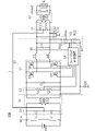
- FIG. 1 is a circuit diagram of a switching power supply device 101 according to the first embodiment.
- FIG. 2 is a circuit diagram of the switching power supply devices 102A and 102B according to the second embodiment.
- FIG. 3 is a circuit diagram of still another switching power supply device 102C, 102D, 102E according to the second embodiment.
- FIG. 4 is a circuit diagram of the switching power supply device 103 according to the third embodiment.
- FIG. 5 is a circuit diagram of the switching power supply device 104 according to the fourth embodiment.
- FIG. 6 is a circuit diagram of the switching power supply device 105 according to the fifth embodiment.
- FIG. 7 is a circuit diagram of the switching power supply device 106 according to the sixth embodiment.
- FIG. 1 is a circuit diagram of a switching power supply device 101 according to the first embodiment.
- the switching power supply device 101 is connected between the DC power supply Vin and the load circuit RL.
- a commercial power system may be connected in parallel to the load circuit RL.
- the switching power supply device 101 includes an inverter circuit 10 and a noise reduction circuit.
- the inverter circuit 10 is an input capacitor Ci connected in parallel between the DC input line DCin, the AC output line ACout, the inductors L1 and L2, the switching circuit 12 for passing a switching current through the inductors L1 and L2, and the DC input line DCin. And the output capacitor Co connected in parallel between the AC output lines ACout, the DC input voltage detection circuit 13 that detects the voltage between the DC input lines DCin, and the AC output voltage detection circuit that detects the voltage between the AC output lines ACout. 15.
- the AC output current detection circuit 16 for detecting the current of the AC output line ACout, and the feedback control circuit 14 are provided.
- the feedback control circuit 14 is composed of an analog circuit or a digital circuit such as an MCU (MicroControllerUnit) or a DSP (DigitalSignalprocessor).
- the feedback control circuit 14 is a switching circuit 12 so that the reference potential is connected to the reference potential line of the DC input line DCin and the AC output voltage or AC output current of the AC output line ACout becomes a predetermined value based on the DC input voltage. To control.
- the noise reduction circuit includes a first half-bridge capacitor circuit 21 connected between DC input lines DCin, a second half-bridge capacitor circuit 22 connected between AC output lines ACout, and a first half-bridge capacitor circuit 21 and a first.
- the first common mode choke coil 31 connected between the two half-bridge capacitor circuits 22 and the middle point of the first half-bridge capacitor circuit 21 and the middle point of the second half-bridge capacitor circuit 22 are electrically connected.
- the electric path 1 and the like are provided.
- the first common mode choke coil 31 is composed of coils L11 and L12 that are magnetically coupled to each other.
- the first half-bridge capacitor circuit 21, the second half-bridge capacitor circuit 22, and the electric path 1 form a noise balancing circuit that balances common mode noise having a potential different from that of ground.
- the noise reduction circuit includes a noise balance circuit and a first common mode choke coil 31.
- the noise balance circuit suppresses the influence of common mode noise on the feedback control circuit 14.
- the midpoint of the first half-bridge capacitor circuit 21 is the intermediate potential of the DC input line DCin
- the midpoint of the second half-bridge capacitor circuit 22 is the intermediate potential of the AC output line ACout
- both intermediate potential portions are common through the electric path 1.
- the electric path 1 is composed of a metal plate. As a result, the voltage drop due to the electric path 1 becomes small, and the potential difference between the midpoint of the first half-bridge capacitor circuit 21 and the midpoint of the second half-bridge capacitor circuit 22 becomes small. Therefore, the equilibration of the common mode noise works more effectively.
- first common mode choke coil 31 is connected between the first half-bridge capacitor circuit 21 and the second half-bridge capacitor circuit 22.
- the first common mode choke coil 31 reduces the current of the common mode noise component generated in the switching circuit 12, and suppresses the influence of the common mode noise on the feedback control circuit 14.
- the feedback control circuit 14 For EMI countermeasures, it is necessary to optimize the capacities of the capacitors C11, C12, C21, and C22. If the capacitor capacity is adjusted (changed), the feedback control circuit 14 is conventionally affected. In this case, the feedback control circuit 14 needs to be redesigned, which prolongs the design period. According to the present embodiment, the current of the common mode noise component generated in the switching circuit 12 has an influence on the feedback control circuit 14 due to the action that the current flowing between the input DC line and the output AC line through the electric path 1 becomes small. small.
- the switching power supply device 101 can also exert the following effects while suppressing the influence of the common mode noise on the feedback control.
- the switching power supply unit 101 can shorten the design period when adjusting (optimizing) the capacity of the capacitors constituting the EMI countermeasure circuit, and realizes a power conversion operation without increasing the leakage current, which is safe. You can secure sex. Further, the switching power supply device 101 can realize a compact and inexpensive configuration.
- Second Embodiment a switching power supply device in which an impedance element is connected to the electric path 1 will be exemplified.
- FIG. 2 is a circuit diagram of the switching power supply devices 102A and 102B according to the second embodiment.
- These switching power supply devices 102A and 102B include an inverter circuit 10, a first half-bridge capacitor circuit 21, a second half-bridge capacitor circuit 22, and a first common mode choke coil 31. Further, an electric path 1 for electrically connecting the midpoint of the first half-bridge capacitor circuit 21 and the midpoint of the second half-bridge capacitor circuit 22 is provided.
- the impedance element Z1 is connected in series to the electric path 1 of the switching power supply device 102A.
- This impedance element Z1 has at least an inductance component or a resistance component.
- An impedance element Z2 is connected between the electric path 1 of the switching power supply device 102B and the ground.
- the impedance element Z2 has at least a capacitance component, an inductance component, or a resistance component.
- This "ground” is a ground or a frame ground.
- the impedance element Z1 By connecting the impedance element Z1 in series to the electric path 1 as in the switching power supply device 102A, even if the effect of suppressing the common mode noise by the first common mode choke coil 31 is insufficient, the impedance element Z1 makes it common. The suppression of mode noise is supplemented. That is, the impedance element Z1 attenuates the vibration of the high frequency common mode current flowing in the electric path 1, and the common mode noise is suppressed.
- the impedance element Z2 is connected between the electric path 1 and the ground.
- the impedance element Z2 has at least a capacitance component, an inductance component, or a resistance component.
- the impedance element Z2 By connecting the impedance element Z2 between the electric path 1 and the ground in this way, even if the effect of suppressing the common mode noise by the first common mode choke coil 31 is insufficient, the impedance element Z2 makes it common.
- the suppression of mode noise is supplemented. That is, the common mode current that flows for the first half-bridge capacitor circuit 21 and the second half-bridge capacitor circuit 22 to balance through the electric path 1 flows to the ground through the impedance element Z2.
- This current (leakage current) is smaller than the current leaking from the line bypass capacitor circuit to the ground when the line bypass capacitor circuit is provided. Therefore, common mode noise can be suppressed while reducing the leakage current.
- FIG. 3 is a circuit diagram of still another switching power supply device 102C, 102D, 102E according to the second embodiment.
- the impedance element Z2 is connected between the electric path 1 and the ground.
- the impedance element Z1 is connected in series between the connection point of the impedance element Z2 with respect to the electric path 1 and the middle point of the second half bridge capacitor circuit 22. Further, in the switching power supply device 102D, the impedance element Z3 is connected in series between the connection point of the impedance element Z2 with respect to the electric path 1 and the middle point of the first half-bridge capacitor circuit 21. In the switching power supply device 102E, the impedance element Z1 is connected in series between the connection point of the impedance element Z2 with respect to the electric path 1 and the midpoint of the second half bridge capacitor circuit 22, and the impedance element Z2 with respect to the electric path 1 is connected. An impedance element Z3 is connected in series between the connection point and the midpoint of the first half-bridge capacitor circuit 21.
- each switching power supply device 102C, 102D, 102E shown in FIG. 3 if the impedance elements Z1 and Z3 are resistors or inductors and the impedance element Z2 is a capacitor, a low-pass filter is configured by these impedance elements. If the impedance elements Z1 and Z3 are capacitors and the impedance elements Z2 are resistors or inductors, these impedance elements constitute a high-pass filter.
- the switching power supply 103 including the second common mode choke coil 32 is exemplified.
- FIG. 4 is a circuit diagram of the switching power supply device 103 according to the third embodiment.
- the switching power supply 103 is connected between the DC power supply Vin and the load circuit RL. Further, the switching power supply device 103 includes an inverter circuit 10 and a noise reduction circuit. In FIG. 4, circuits other than the inverter circuit 10 constitute a noise reduction circuit.
- the switching power supply 103 includes a second common mode choke coil 32 connected to the load side of the second half-bridge capacitor circuit 22.
- Other configurations are the same as those of the switching power supply device 101 shown in FIG.
- the second common mode choke coil 32 is composed of coils L21 and L22 that are magnetically coupled to each other.
- the second common mode choke coil 32 suppresses common mode noise superimposed on the AC output line ACout of the inverter circuit 10.
- FIG. 5 is a circuit diagram of the switching power supply device 104 according to the fourth embodiment.
- the switching power supply device 104 is connected between the DC power supply Vin and the load circuit RL. Further, the switching power supply device 104 includes an inverter circuit 10 and a noise reduction circuit. In FIG. 5, circuits other than the inverter circuit 10 constitute a noise reduction circuit.
- the switching power supply device 104 includes two capacitors C31 and C32 connected in series, and this circuit is connected between AC output lines ACout, and the midpoint is connected to ground. Other configurations are the same as those of the switching power supply device 103 shown in FIG.
- the circuit by the capacitors C31 and C32 suppresses the common mode noise superimposed on the AC output line ACout of the inverter circuit 10.
- a switching power supply device including a capacitor C4 connected between the reference potential of the feedback control circuit 14 and the electric path 1 will be illustrated.
- FIG. 6 is a circuit diagram of the switching power supply device 105 according to the fifth embodiment.
- the switching power supply device 105 is connected between the DC power supply Vin and the load circuit RL. Further, the switching power supply device 105 includes an inverter circuit 10 and a noise reduction circuit. In FIG. 6, circuits other than the inverter circuit 10 constitute a noise reduction circuit.
- the switching power supply device 105 includes a capacitor C4 connected between the reference potential of the feedback control circuit 14 and the electric path 1.
- Other configurations are the same as those of the switching power supply device 104 shown in FIG.
- the capacitor C4 By connecting the capacitor C4 between the reference potential of the feedback control circuit 14 and the electric path 1, the potential of the electric path 1 is stabilized, and the electric path detects voltage and current while suppressing common mode noise. The influence on the signal line can be reduced.
- a sixth embodiment illustrates a switching power supply device including a capacitor C5 connected between the reference potential of the feedback control circuit 14 and ground.
- FIG. 7 is a circuit diagram of the switching power supply device 106 according to the sixth embodiment.
- the switching power supply device 106 is connected between the DC power supply Vin and the load circuit RL. Further, the switching power supply device 106 includes an inverter circuit 10 and a noise reduction circuit. In FIG. 7, a circuit other than the inverter circuit 10 constitutes a noise reduction circuit.
- the switching power supply device 106 includes a capacitor C5 connected between the reference potential of the feedback control circuit 14 and the ground.
- Other configurations are the same as those of the switching power supply device 104 shown in FIG.
- the capacitor C5 By connecting the capacitor C5 between the reference potential of the feedback control circuit 14 and the ground, the potential of the electric path 1 is stabilized, and the electric path 1 is a voltage or current detection signal while suppressing common mode noise. The effect on the line can be reduced.
Landscapes
- Engineering & Computer Science (AREA)
- Power Engineering (AREA)
- Physics & Mathematics (AREA)
- Electromagnetism (AREA)
- Inverter Devices (AREA)
Priority Applications (2)
| Application Number | Priority Date | Filing Date | Title |
|---|---|---|---|
| JP2022572128A JP7597127B2 (ja) | 2020-12-21 | 2021-12-10 | スイッチング電源装置 |
| US18/335,075 US12368373B2 (en) | 2020-12-21 | 2023-06-14 | Switching power supply device |
Applications Claiming Priority (2)
| Application Number | Priority Date | Filing Date | Title |
|---|---|---|---|
| JP2020-210981 | 2020-12-21 | ||
| JP2020210981 | 2020-12-21 |
Related Child Applications (1)
| Application Number | Title | Priority Date | Filing Date |
|---|---|---|---|
| US18/335,075 Continuation US12368373B2 (en) | 2020-12-21 | 2023-06-14 | Switching power supply device |
Publications (1)
| Publication Number | Publication Date |
|---|---|
| WO2022138215A1 true WO2022138215A1 (ja) | 2022-06-30 |
Family
ID=82157910
Family Applications (1)
| Application Number | Title | Priority Date | Filing Date |
|---|---|---|---|
| PCT/JP2021/045424 Ceased WO2022138215A1 (ja) | 2020-12-21 | 2021-12-10 | スイッチング電源装置 |
Country Status (3)
| Country | Link |
|---|---|
| US (1) | US12368373B2 (https=) |
| JP (1) | JP7597127B2 (https=) |
| WO (1) | WO2022138215A1 (https=) |
Families Citing this family (1)
| Publication number | Priority date | Publication date | Assignee | Title |
|---|---|---|---|---|
| WO2023013343A1 (ja) * | 2021-08-02 | 2023-02-09 | 株式会社村田製作所 | スイッチング電源装置 |
Citations (3)
| Publication number | Priority date | Publication date | Assignee | Title |
|---|---|---|---|---|
| JP2012065515A (ja) * | 2010-09-17 | 2012-03-29 | Toshiba Corp | 電力変換装置のスイッチング方法 |
| JP2015204407A (ja) * | 2014-04-15 | 2015-11-16 | 株式会社神戸製鋼所 | ノイズ低減用巻線素子およびインバータ装置 |
| JP2018191369A (ja) * | 2017-04-28 | 2018-11-29 | 三菱電機株式会社 | 系統連系インバータ |
Family Cites Families (10)
| Publication number | Priority date | Publication date | Assignee | Title |
|---|---|---|---|---|
| US6850423B2 (en) * | 2003-05-30 | 2005-02-01 | Comarco Wireless Technologies, Inc. | Common mode noise cancellation circuit |
| JP5468394B2 (ja) * | 2010-01-13 | 2014-04-09 | 株式会社東芝 | 系統連系インバータ |
| JP6191542B2 (ja) | 2014-05-21 | 2017-09-06 | 株式会社デンソー | 電力変換装置 |
| JP2016158316A (ja) | 2015-02-23 | 2016-09-01 | 株式会社豊田自動織機 | 電源装置 |
| JP6260578B2 (ja) | 2015-04-17 | 2018-01-17 | トヨタ自動車株式会社 | 送電装置及び受電装置 |
| US10193488B2 (en) * | 2016-01-14 | 2019-01-29 | Regal Beloit America, Inc. | Methods and systems for reducing conducted electromagnetic interference |
| JP6437499B2 (ja) * | 2016-09-15 | 2018-12-12 | 三菱電機株式会社 | 電力変換装置 |
| JP6825627B2 (ja) * | 2016-10-04 | 2021-02-03 | 住友電気工業株式会社 | 電力変換装置及び電流歪の低減方法 |
| DE102017110608A1 (de) * | 2017-05-16 | 2018-11-22 | Valeo Siemens Eautomotive Germany Gmbh | Inverter |
| WO2019130874A1 (ja) * | 2017-12-27 | 2019-07-04 | 株式会社村田製作所 | 電源装置 |
-
2021
- 2021-12-10 WO PCT/JP2021/045424 patent/WO2022138215A1/ja not_active Ceased
- 2021-12-10 JP JP2022572128A patent/JP7597127B2/ja active Active
-
2023
- 2023-06-14 US US18/335,075 patent/US12368373B2/en active Active
Patent Citations (3)
| Publication number | Priority date | Publication date | Assignee | Title |
|---|---|---|---|---|
| JP2012065515A (ja) * | 2010-09-17 | 2012-03-29 | Toshiba Corp | 電力変換装置のスイッチング方法 |
| JP2015204407A (ja) * | 2014-04-15 | 2015-11-16 | 株式会社神戸製鋼所 | ノイズ低減用巻線素子およびインバータ装置 |
| JP2018191369A (ja) * | 2017-04-28 | 2018-11-29 | 三菱電機株式会社 | 系統連系インバータ |
Also Published As
| Publication number | Publication date |
|---|---|
| US20230327539A1 (en) | 2023-10-12 |
| US12368373B2 (en) | 2025-07-22 |
| JPWO2022138215A1 (https=) | 2022-06-30 |
| JP7597127B2 (ja) | 2024-12-10 |
Similar Documents
| Publication | Publication Date | Title |
|---|---|---|
| US7994876B2 (en) | Lightweight electromagnetic interference filter | |
| US20140347159A1 (en) | Transformer | |
| JP4351916B2 (ja) | ノイズフィルタ | |
| JPH10512063A (ja) | 力率訂正回路のためのダンピングされたemi入力フィルタ | |
| EP2724168B1 (en) | A noise sensor | |
| JP2012044812A (ja) | ノイズフィルタ及びこれを使用したemcフィルタ | |
| JP5916390B2 (ja) | 電源ユニット及びそれを用いたled照明装置 | |
| JP2008512022A (ja) | 線伝導妨害信号を抑制するアクティブ電磁妨害フィルタ回路 | |
| JP7597127B2 (ja) | スイッチング電源装置 | |
| JP4231825B2 (ja) | ノイズ抑制回路 | |
| JP7400995B2 (ja) | 力率改善スイッチング電源装置 | |
| JP7563487B2 (ja) | スイッチング電源装置 | |
| JP2009148045A (ja) | 漏洩電流低減装置 | |
| CN110603724B (zh) | 电源电路 | |
| JP6239468B2 (ja) | 医療装置 | |
| TW202220353A (zh) | 電磁干擾抑制電路及相關的感測電路 | |
| JP7677241B2 (ja) | 非接触給電システム | |
| JP7012185B1 (ja) | 電圧検知回路 | |
| JP4275034B2 (ja) | ノイズ抑制回路 | |
| WO2019102937A1 (ja) | ノイズフィルタ回路、及び、電源回路 | |
| WO2026071059A1 (ja) | ノイズフィルタ、電力変換システム、ヒートポンプ装置、パッシブフィルタ基板およびアクティブノイズキャンセラ基板 | |
| JP7012231B2 (ja) | 電源回路 | |
| WO2026070407A1 (ja) | ノイズ低減装置および空気調和装置 | |
| JPH03186007A (ja) | ラインフィルタ | |
| JP2012015849A (ja) | ノーマルモードリアクトルおよびこれを備えた電力変換装置 |
Legal Events
| Date | Code | Title | Description |
|---|---|---|---|
| 121 | Ep: the epo has been informed by wipo that ep was designated in this application |
Ref document number: 21910364 Country of ref document: EP Kind code of ref document: A1 |
|
| ENP | Entry into the national phase |
Ref document number: 2022572128 Country of ref document: JP Kind code of ref document: A |
|
| NENP | Non-entry into the national phase |
Ref country code: DE |
|
| 122 | Ep: pct application non-entry in european phase |
Ref document number: 21910364 Country of ref document: EP Kind code of ref document: A1 |