WO2022137705A1 - 電圧検知回路 - Google Patents
電圧検知回路 Download PDFInfo
- Publication number
- WO2022137705A1 WO2022137705A1 PCT/JP2021/036020 JP2021036020W WO2022137705A1 WO 2022137705 A1 WO2022137705 A1 WO 2022137705A1 JP 2021036020 W JP2021036020 W JP 2021036020W WO 2022137705 A1 WO2022137705 A1 WO 2022137705A1
- Authority
- WO
- WIPO (PCT)
- Prior art keywords
- voltage
- circuit
- output
- input
- buffer
- Prior art date
- Legal status (The legal status is an assumption and is not a legal conclusion. Google has not performed a legal analysis and makes no representation as to the accuracy of the status listed.)
- Ceased
Links
Images




Classifications
-
- G—PHYSICS
- G01—MEASURING; TESTING
- G01R—MEASURING ELECTRIC VARIABLES; MEASURING MAGNETIC VARIABLES
- G01R19/00—Arrangements for measuring currents or voltages or for indicating presence or sign thereof
- G01R19/165—Indicating that current or voltage is either above or below a predetermined value or within or outside a predetermined range of values
- G01R19/16533—Indicating that current or voltage is either above or below a predetermined value or within or outside a predetermined range of values characterised by the application
- G01R19/16538—Indicating that current or voltage is either above or below a predetermined value or within or outside a predetermined range of values characterised by the application in AC or DC supplies
- G01R19/16542—Indicating that current or voltage is either above or below a predetermined value or within or outside a predetermined range of values characterised by the application in AC or DC supplies for batteries
-
- G—PHYSICS
- G01—MEASURING; TESTING
- G01R—MEASURING ELECTRIC VARIABLES; MEASURING MAGNETIC VARIABLES
- G01R19/00—Arrangements for measuring currents or voltages or for indicating presence or sign thereof
- G01R19/165—Indicating that current or voltage is either above or below a predetermined value or within or outside a predetermined range of values
- G01R19/16566—Circuits and arrangements for comparing voltage or current with one or several thresholds and for indicating the result not covered by subgroups G01R19/16504, G01R19/16528, G01R19/16533
-
- G—PHYSICS
- G01—MEASURING; TESTING
- G01R—MEASURING ELECTRIC VARIABLES; MEASURING MAGNETIC VARIABLES
- G01R31/00—Arrangements for testing electric properties; Arrangements for locating electric faults; Arrangements for electrical testing characterised by what is being tested not provided for elsewhere
- G01R31/36—Arrangements for testing, measuring or monitoring the electrical condition of accumulators or electric batteries, e.g. capacity or state of charge [SoC]
- G01R31/385—Arrangements for measuring battery or accumulator variables
- G01R31/387—Determining ampere-hour charge capacity or SoC
- G01R31/388—Determining ampere-hour charge capacity or SoC involving voltage measurements
-
- G—PHYSICS
- G01—MEASURING; TESTING
- G01R—MEASURING ELECTRIC VARIABLES; MEASURING MAGNETIC VARIABLES
- G01R15/00—Details of measuring arrangements of the types provided for in groups G01R17/00 - G01R29/00, G01R33/00 - G01R33/26 or G01R35/00
- G01R15/04—Voltage dividers
-
- G—PHYSICS
- G01—MEASURING; TESTING
- G01R—MEASURING ELECTRIC VARIABLES; MEASURING MAGNETIC VARIABLES
- G01R31/00—Arrangements for testing electric properties; Arrangements for locating electric faults; Arrangements for electrical testing characterised by what is being tested not provided for elsewhere
- G01R31/36—Arrangements for testing, measuring or monitoring the electrical condition of accumulators or electric batteries, e.g. capacity or state of charge [SoC]
- G01R31/382—Arrangements for monitoring battery or accumulator variables, e.g. SoC
- G01R31/3835—Arrangements for monitoring battery or accumulator variables, e.g. SoC involving only voltage measurements
-
- G—PHYSICS
- G01—MEASURING; TESTING
- G01R—MEASURING ELECTRIC VARIABLES; MEASURING MAGNETIC VARIABLES
- G01R35/00—Testing or calibrating of apparatus covered by the other groups of this subclass
Definitions
- the present invention relates to a voltage detection circuit.
- the DC power supplied from the high-voltage battery is converted into AC power by an inverter, output to the AC motor for driving, and the motor is driven to rotate. It is equipped with an electric system to make it.
- a voltage detection circuit that detects the voltage of a high voltage battery is widely used.
- the voltage information of the high-voltage battery detected by the voltage detection circuit is used for charge control of the high-voltage battery and control of the inverter.
- the voltage detection circuit is required to have a failure detection function capable of detecting the failure by itself when the failure occurs.
- Patent Document 1 As a related technique of the present invention, the technique described in Patent Document 1 is known.
- voltage dividing resistors are connected to the positive and negative sides of the DC power supply, respectively, and in a voltage detection device that detects the voltage of the DC power supply through these voltage dividing resistors, pulses having different polarities are transmitted to each other.
- a technique for detecting a failure of a voltage dividing resistance by observing a voltage fluctuation when the voltage dividing value of each voltage dividing resistance is changed in addition to the voltage dividing resistance is disclosed.
- An object of the present invention is to provide a voltage detection circuit capable of realizing a variety of abnormality diagnoses as compared with the conventional one, in order to solve the problems of the prior art.
- the voltage detection circuit includes a first buffer circuit and a second buffer circuit that output a voltage corresponding to an input voltage, an output voltage of the first buffer circuit, and an output voltage of the second buffer circuit, respectively.
- a voltage detector that detects voltage, a reference voltage output circuit that can selectively output any of a plurality of reference voltages having different voltage values, and a switch connected to the first buffer circuit and the second buffer circuit.
- the switch circuit comprises a circuit, wherein the switch circuit sets the input voltage of the first buffer circuit from the first input voltage corresponding to the voltage of the first input terminal connected to the measurement target to the reference voltage output circuit.
- the reference voltage is switched to the reference voltage output from, and the input voltage of the second buffer circuit is output from the second input voltage corresponding to the voltage of the second input terminal connected to the measurement target. It switches to the reference voltage output from the circuit.
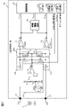
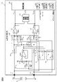
- FIG. 1 is a block diagram of a voltage detection circuit according to the first embodiment of the present invention.
- the voltage detection circuit 1 according to the present embodiment is connected to the high voltage battery 2 and detects the voltage of the high voltage battery 2 input via the positive electrode input terminal 11 and the negative electrode input terminal 12.
- the voltage detection circuit 1 includes a positive electrode input terminal 11, a negative negative input terminal 12, a reference voltage output circuit 13, a voltage divider circuit 14, a voltage divider circuit 15, a switch circuit 16, a buffer circuit 17, and a buffer circuit 18. , A differential amplifier circuit 19 and a control circuit 20.
- the positive electrode input terminal 11 is connected to the positive electrode side of the high voltage battery 2, and the positive electrode voltage Vp of the high voltage battery 2 is input.
- the negative electrode input terminal 12 is connected to the negative electrode side of the high voltage battery 2, and the negative electrode voltage Vn of the high voltage battery 2 is input.
- the reference voltage output circuit 13 has a switch element SW1, resistors R1, R2 and R3, and an operational amplifier AMP1.
- the resistors R1, R2, and R3 are connected in series to form a voltage divider circuit, one end side of the voltage divider circuit is connected to a predetermined power supply voltage, and the other end side is grounded.
- the operational amplifier AMP1 functions as a voltage follower (buffer circuit) that outputs the same voltage as the input voltage and lowers the impedance on the output side.
- a voltage tracker IC or the like may be used instead of the operational amplifier.
- the input terminal of the operational amplifier AMP1 is connected between the resistors R1 and R2, and the reference voltage Vref obtained by dividing the power supply voltage by the voltage dividing circuit described above is input as the input voltage of the operational amplifier AMP1.
- the operational amplifier AMP1 outputs the same offset voltage Voffset as the reference voltage Vref
- the predetermined reference voltage Vref offset voltage Voffset
- Voffset offset voltage Voffset
- the switch element SW1 is switched to either an on state or an off state according to the offset switching signal output from the control circuit 20.
- the connection state of the resistor R3 in the voltage divider circuit is switched, the voltage divider ratio of the voltage divider circuit changes, and the value of the reference voltage Vref changes according to the voltage divider ratio. That is, the reference voltage output circuit 13 is configured to be able to selectively output one of two types of reference voltages having different voltage values by switching the switch element SW1 on / off.
- the configuration of the reference voltage output circuit 13 shown in FIG. 1 is an example, and if one of two types of reference voltages having different voltage values can be selectively output, another configuration is adopted. May be good.
- another configuration example of the reference voltage output circuit 13 will be described with reference to FIG.
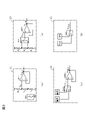
- FIG. 2 is a diagram showing various configuration examples of the reference voltage output circuit 13.
- FIG. 2A shows a reference voltage output circuit 13 having the same configuration as that shown in FIG.
- the reference voltage output circuit 13 in the reference voltage output circuit 13, one end side of the switch element SW1 is connected between the resistance R1 and the resistance R2, and the other end side is connected between the resistance R2 and the resistance R3.
- the reference voltage output circuit 13 has two types of power supply circuits that output different power supply voltages instead of the voltage divider circuit in which the resistors R1, R2, and R3 are connected in series.
- a switch element SW1 is installed between these power supply circuits and the input terminal of the operational amplifier AMP1.
- the operational amplifier AMP1 is removed from the circuit configuration of FIG. 2C in the reference voltage output circuit 13.
- the reference voltage output circuit 13 switches the switch element SW1 according to the offset switching signal output from the control circuit 20. Any one of the two types of reference voltage Vref can be selectively output as the offset voltage Switch.
- the two types of reference voltage Vrefs output by the reference voltage output circuit 13 will be described as Vref1 and Vref2, respectively.
- the reference voltage output circuit 13 that selectively outputs either the reference voltage Vref1 or Vref2 as the offset voltage Voffset according to the switching operation of the switch element SW1 has been described, but three or more types have been described. Any one of the reference voltage Vrefs of the above may be selectively output from the reference voltage output circuit 13. Further, as long as a plurality of types of reference voltages can be selectively output, not only the circuit configuration shown in each example of FIG. 2 but also any circuit configuration can be adopted in the reference voltage output circuit 13. ..
- the voltage dividing circuit 14 is composed of a resistor R4 and a resistor R5, and is connected between the positive electrode input terminal 11 and the reference voltage output circuit 13.
- a buffer circuit 17 is connected between the resistors R4 and R5 via a switch circuit 16.
- the positive electrode voltage Vp input to the positive electrode input terminal 11 is divided by the voltage dividing circuit 14 at a predetermined voltage dividing ratio, and is output to the buffer circuit 17 via the switch circuit 16.
- the voltage dividing circuit 15 is composed of a resistor R6 and a resistor R7, and is connected between the negative electrode input terminal 12 and the reference voltage output circuit 13.
- a buffer circuit 18 is connected between the resistors R6 and R7 via a switch circuit 16.
- the negative electrode voltage Vn input to the negative electrode input terminal 12 is divided by the voltage dividing circuit 15 at a predetermined voltage dividing ratio, and is output to the buffer circuit 18 via the switch circuit 16.
- the offset voltage Voffset output from the reference voltage output circuit 13 is applied to the opposite sides of the positive electrode input terminal 11 and the negative electrode input terminal 12, respectively.
- the voltages generated by the voltage dividing circuits 14 and 15, respectively can be offset according to the offset voltage Voffset.
- the switch circuit 16 is connected between the reference voltage output circuit 13 and the voltage dividing circuit 14 and the buffer circuit 17, and between the reference voltage output circuit 13 and the voltage dividing circuit 15 and the buffer circuit 18.
- the switch circuit 16 has a switch element SW2-1 and a switch element SW2-2.
- the switch element SW2-1 is connected to the voltage dividing circuit 14 and the buffer circuit 17, and the connection destination of the input terminal of the buffer circuit 17 is divided in voltage according to the normal / diagnostic switching signal output from the control circuit 20. It is switched to either the positive electrode input terminal 11 side via the circuit 14 or the reference voltage output circuit 13 side.
- the positive voltage Vp of the positive positive input terminal 11 is output as the input voltage of the buffer circuit 17 from the voltage divided by the voltage dividing circuit 14 or from the reference voltage output circuit 13.
- Either the offset voltage Voffset reference voltage Vref1 or Vref2
- the switch element SW2-2 is connected to the voltage dividing circuit 15 and the buffer circuit 18, and the connection destination of the input terminal of the buffer circuit 18 is divided in voltage according to the normal / diagnostic switching signal output from the control circuit 20. It is switched to either the negative electrode input terminal 12 side via the circuit 15 or the reference voltage output circuit 13 side. By the switching operation of the switch element SW2-2, the negative voltage Vn of the negative negative input terminal 12 is output as the input voltage of the buffer circuit 18 from the voltage divided by the voltage dividing circuit 15 or from the reference voltage output circuit 13. Either the offset voltage Voffset (reference voltage Vref1 or Vref2) is selected.
- the buffer circuit 17 has a function of outputting the same voltage with respect to the input voltage and lowering the impedance on the output side, and is configured by a voltage follower using an operational amplifier AMP2.
- the buffer circuit 17 may be configured by using a voltage tracker IC or the like instead of the voltage follower.
- the output voltage V HVPC of the buffer circuit 17 is input to the differential amplifier circuit 19 and the control circuit 20.
- the buffer circuit 18 has a function of outputting the same voltage with respect to the input voltage and lowering the impedance on the output side, and is configured by a voltage follower using an operational amplifier AMP3.
- the buffer circuit 18 may be configured by using a voltage tracker IC or the like instead of the voltage follower.
- the output voltage V HVNC of the buffer circuit 18 is input to the differential amplifier circuit 19 and the control circuit 20.
- the voltage output by the buffer circuits 17 and 18 may be a voltage corresponding to the input voltage, and does not necessarily have to be the same voltage as the input voltage.
- the differential amplifier circuit 19 detects the difference between the output voltage V HVPC of the buffer circuit 17 and the output voltage V HVNC of the buffer circuit 18, and outputs the differential voltage V HVDC corresponding to the difference to the control circuit 20.
- the difference between the positive electrode voltage Vp of the positive electrode input terminal 11 and the negative electrode voltage Vn of the negative electrode input terminal 12, that is, the differential voltage V HVDC corresponding to the voltage of the high voltage battery 2 is output from the differential amplifier circuit 19 and controlled. It is input to the circuit 20.
- the control circuit 20 is a circuit that performs overall control of the voltage detection circuit 1, and has a voltage detection unit 20A, a switching signal control unit 20B, and an abnormality detection unit 20C as its functions.
- the control circuit 20 can realize these functions by, for example, executing a predetermined program in a microcomputer or using a logic circuit such as FPGA (Field-Programmable Gate Array).
- the voltage detection unit 20A detects the differential voltage V HVDC output from the differential amplifier circuit 19, and based on this, detects the voltage between the positive and negative electrodes of the high voltage battery 2. Further, the voltage detection unit 20A detects the output voltages V HVPC and V HVNC of the buffer circuits 17 and 18 and the offset voltage Voffset (reference voltage Vref1 or Vref2) output from the reference voltage output circuit 13.
- the switching signal control unit 20B controls an offset switching signal output to the switch element SW1 of the reference voltage output circuit 13 and a normal / diagnostic switching signal output to the switch circuit 16. By controlling these switching signals, the switching signal control unit 20B switches the value of the offset voltage Voffset output from the reference voltage output circuit 13 to either the reference voltage Vref1 or Vref2, and switches element SW2- in the switch circuit 16. By controlling the switching state of 1, SW2-2, the connection destination of the input terminals of the buffer circuits 17 and 18 is switched to either the positive electrode input terminal 11 and the negative electrode input terminal 12 side or the reference voltage output circuit 13 side. Can be done.
- the abnormality detection unit 20C acquires the output voltages V HVPC , V HVNC of the buffer circuits 17 and 18 acquired by the voltage detection unit 20A and the offset voltage Voffset which is the output voltage of the reference voltage output circuit 13, and uses these voltage values. Based on this, the abnormality of the voltage detection circuit 1 is detected.
- the control circuit 20 transmits a predetermined abnormality flag to a higher-level device (not shown) to notify that the abnormality has occurred in the voltage detection circuit 1.
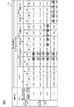
- FIG. 3 is an expected value table for diagnosing an amplifier abnormality.
- the table shown in FIG. 3 shows the case where the voltage detection circuit 1 is normal and the case where the reference voltage Vref and the operational amplifier AMP1 of the reference voltage output circuit 13 and the operational amplifiers AMP2 and AMP3 of the buffer circuits 17 and 18 are abnormal, respectively.
- What are the reference voltage Vref, offset voltage Voffset, and output voltages V HVPC and V HVNC of the buffer circuits 17 and 18 according to the switching state of the switch circuit 16 and the switch element SW1 by the normal / diagnostic switching signal and the offset switching signal, respectively? Indicates whether to take a value.
- the switch circuit 16 In the normal control for detecting the voltage of the high voltage battery 2, in the switching signal control unit 20B, the switch circuit 16 is on the normal side, that is, the input terminals of the buffer circuits 17 and 18 are connected to the positive input terminals via the voltage divider circuits 14 and 15. A normal / diagnostic switching signal is output so as to be connected to 11 and the negative voltage input terminal 12, respectively. Further, the offset switching signal is output so that the switch element SW1 of the reference voltage output circuit 13 is switched to the off state and the reference voltage Vref1 is output as the offset voltage Voffset from the reference voltage output circuit 13.
- the voltage detection unit 20A detects the reference voltage Vref1 as the offset voltage Voffset. Further, as the output voltage V HVPC of the buffer circuit 17, the voltage value obtained by dividing the positive voltage Vp by the voltage dividing ratio corresponding to the resistance values of the resistors R4 and R5 of the voltage dividing circuit 14 is further added to the reference voltage Vref1 (offset voltage Voffset). Only the offset voltage value is detected.
- the voltage value obtained by dividing the negative voltage Vn by the voltage dividing ratio corresponding to the resistance values of the resistors R6 and R7 of the voltage dividing circuit 15 is further added to the reference voltage Vref1 (offset voltage Voffset). ) Offset voltage value is detected.
- the switch circuit 16 is connected to the diagnosis side, that is, the input terminals of the buffer circuits 17 and 18 are connected to the output terminals of the reference voltage output circuit 13, respectively.
- the normal / diagnostic switching signal is output.
- the switch element SW1 of the reference voltage output circuit 13 is switched between the off state and the on state, respectively, and the reference voltage Vref1 and Vref2 are output as the offset voltage Voffset from the reference voltage output circuit 13 accordingly. , Outputs the offset switching signal.
- the voltage detection unit 20A detects the reference voltage Vref1 as the offset voltage Voffset.
- the reference voltage Vref1 is input to the buffer circuits 17 and 18 via the switch circuit 16
- the reference voltage Vref1 is also detected in the output voltages V HVPC and V HVNC of the buffer circuits 17 and 18, respectively.
- the voltage detection unit 20A detects a value other than the reference voltage Vref1 as the offset voltage Voffset. Further, values other than the reference voltage Vref1 are also detected in the output voltages V HVPC and V HVNC of the buffer circuits 17 and 18, respectively.
- the output voltage of the reference voltage output circuit 13 is not the reference voltage Vref1. Therefore, in this case as well, a value other than the reference voltage Vref1 is detected as the offset voltage Voffset by the voltage detection unit 20A, as in the case of the above-mentioned abnormality of the reference voltage Vref. Further, values other than the reference voltage Vref1 are also detected in the output voltages V HVPC and V HVNC of the buffer circuits 17 and 18, respectively.
- the voltage detection unit 20A detects a value other than the reference voltage Vref1 as the output voltage V HVPC of the buffer circuit 17. Similarly, when an abnormality occurs in the operational amplifier AMP3 in the buffer circuit 18, the voltage detection unit 20A detects a value other than the reference voltage Vref1 as the output voltage V HVNC of the buffer circuit 18.
- Vref1 is replaced with Vref2. Is the same as above. That is, when the switch element SW1 of the reference voltage output circuit 13 is in the ON state, if the reference voltage Vref and the operational amplifiers AMP1 to AMP3 are both normal, the voltage detection unit 20A detects the reference voltage Vref2 as the offset voltage Voffset. , The reference voltage Vref2 is also detected in the output voltages V HVPC and V HVNC of the buffer circuits 17 and 18, respectively. On the other hand, when any of the reference voltage Vref or the operational amplifiers AMP1 to AMP3 is abnormal, a value other than the reference voltage Vref2 is detected at the voltage corresponding to the abnormal portion.
- FIG. 4 is an expected value table for switch sticking diagnosis.
- the table shown in FIG. 4 shows the case where the voltage detection circuit 1 is normal and the case where the switch element SW1 of the reference voltage output circuit 13 and the switch elements SW2-1 and SW2-2 of the switch circuit 16 are abnormal, respectively.
- What are the reference voltage Vref, offset voltage Voffset, and output voltages V HVPC and V HVNC of the buffer circuits 17 and 18 according to the switching state of the switch circuit 16 and the switch element SW1 by the normal / diagnostic switching signal and the offset switching signal, respectively? Indicates whether to take a value.
- the reference voltage Vref and the operational amplifiers AMP1 to AMP3 are both normal, the voltage values when each switch element is normal and when the sticking is abnormal are shown.
- the switching signal control unit 20B outputs a normal / diagnostic switching signal so that the switch circuit 16 is switched to the normal side and then switched to the diagnostic side. Output.
- the switching order between the normal side and the diagnostic side may be exchanged.
- the switch element SW1 of the reference voltage output circuit 13 is switched between the off state and the on state, respectively, and the reference voltage Vref1 and Vref2 are set as the offset voltage Voffset from the reference voltage output circuit 13 accordingly. Is output so that the offset switching signal is output.
- the voltage detection unit 20A sets the offset voltage Voffset and the output voltages V HVPC and V HVNC of the buffer circuits 17 and 18 as shown in FIG. The same voltage as in the normal state shown is detected.
- the offset switching signal is changed when the switch circuit 16 is switched to the diagnostic side.
- the value of the reference voltage Vref remains Vref1 and does not change. Therefore, when the offset switching signal for switching the switch element SW1 to the reference voltage Vref2 side is output, the voltage detection unit 20A detects the reference voltage Vref1 as the offset voltage Voffset instead of the original reference voltage Vref2.
- the reference voltage Vref1 is detected instead of the original reference voltage Vref2, respectively.
- the offset switching signal is changed when the switch circuit 16 is switched to the diagnostic side.
- the value of the reference voltage Vref remains Vref2 and does not change. Therefore, when the offset switching signal for switching the switch element SW1 to the reference voltage Vref1 side is output, the voltage detection unit 20A detects the reference voltage Vref2 as the offset voltage Voffset instead of the original reference voltage Vref1.
- the switch circuit 16 when an abnormality occurs in which the switch element SW2-1 is stuck to the diagnosis side, that is, the reference voltage output circuit 13 side, even if the normal / diagnosis switching signal is changed, the reference voltage is displayed in the buffer circuit 17.
- the offset voltage Switch from the output circuit 13 continues to be input. Therefore, when the normal / diagnostic switching signal for switching the switch circuit 16 to the normal side is output, the voltage detection unit 20A uses the output voltage V HVPC of the buffer circuit 17 as the voltage value corresponding to the original positive voltage Vp. Instead, the reference voltage Vref1 or Vref2 is detected according to the offset switching signal.
- the buffer circuit 17 has a positive electrode.
- the voltage whose voltage Vp is divided by the voltage dividing circuit 14 continues to be input. Therefore, when the normal / diagnostic switching signal for switching the switch circuit 16 to the diagnostic side is output, the voltage detection unit 20A sets the output voltage V HVPC of the buffer circuit 17 to a voltage value other than the original reference voltage Vref1 or Vref2. Is detected.
- the switch circuit 16 when an abnormality occurs in which the switch element SW2-2 is stuck to the diagnostic side, that is, the reference voltage output circuit 13 side, even if the normal / diagnostic switching signal is changed, the buffer circuit 18 has a reference voltage.
- the offset voltage Switch from the output circuit 13 continues to be input. Therefore, when the normal / diagnostic switching signal for switching the switch circuit 16 to the normal side is output, the voltage detection unit 20A sets the output voltage V HVNC of the buffer circuit 18 to the voltage value corresponding to the original negative voltage Vn. Instead, the reference voltage Vref1 or Vref2 is detected according to the offset switching signal.
- the buffer circuit 18 has a negative electrode.
- the voltage whose voltage Vn is divided by the voltage dividing circuit 15 continues to be input. Therefore, when the normal / diagnostic switching signal for switching the switch circuit 16 to the diagnostic side is output, the voltage detection unit 20A sets the output voltage V HVNC of the buffer circuit 18 to a voltage value other than the original reference voltage Vref1 or Vref2. Is detected.
- the reference voltages Vref1 and Vref2 of the reference voltage output circuit 13 can be stored as known values.
- each voltage value detected by the voltage detection unit 20A when the normal / diagnostic switching signal and the offset switching signal are changed that is, the offset voltage Voffset and the output voltage V HVPC of the buffer circuits 17 and 18,
- the value of V HVNC is acquired and compared with the expected value table of FIGS. 3 and 4. As a result, when a voltage value different from the normal state is detected, it can be determined that one of the circuits constituting the voltage detection circuit 1 is abnormal according to these expected value tables.
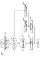
- FIG. 5 is a flowchart showing the procedure of abnormality diagnosis executed by the control circuit 20.
- step S101 the inputs of the buffer circuits 17 and 18 are switched to the reference voltage output circuit 13 side.
- the switching signal control unit 20B outputs a normal / diagnostic switching signal so that the switch circuit 16 can be switched to the diagnostic side, thereby switching the inputs of the buffer circuits 17 and 18.
- step S102 the reference voltage in the reference voltage output circuit 13 is switched to Vref1.
- the switching signal control unit 20B switches the switch element SW1 to the off state in the reference voltage output circuit 13, and the reference voltage Vref1 is output as the offset voltage Voffset from the reference voltage output circuit 13 accordingly. Outputs an offset switching signal.
- step S103 the voltage detection unit 20A measures the voltage of each circuit unit.
- the value of the offset voltage Voffset output from the reference voltage output circuit 13 and the output voltages V HVPC and V HVNC of the buffer circuits 17 and 18 are measured.
- step S104 the reference voltage in the reference voltage output circuit 13 is switched to Vref2.
- the switching signal control unit 20B switches the switch element SW1 to the ON state in the reference voltage output circuit 13, and the reference voltage Vref2 is output as the offset voltage Voffset from the reference voltage output circuit 13 accordingly. Outputs an offset switching signal.
- step S105 the voltage detection unit 20A measures the value of the offset voltage Voffset output from the reference voltage output circuit 13 and the output voltages V HVPC and V HVNC of the buffer circuits 17 and 18.
- step S106 the inputs of the buffer circuits 17 and 18 are switched to the voltage dividing circuits 14 and 15.
- the switching signal control unit 20B outputs a normal / diagnostic switching signal so that the switch circuit 16 can be switched to the normal side, thereby switching the inputs of the buffer circuits 17 and 18.
- step S107 the reference voltage in the reference voltage output circuit 13 is switched to Vref 1 as in step S102.
- step S108 the voltage detection unit 20A measures the value of the offset voltage Voffset output from the reference voltage output circuit 13 and the output voltages V HVPC and V HVNC of the buffer circuits 17 and 18.
- step S109 the reference voltage in the reference voltage output circuit 13 is switched to Vref2 in the same manner as in step S104.
- step S110 the voltage detection unit 20A measures the value of the offset voltage Voffset output from the reference voltage output circuit 13 and the output voltages V HVPC and V HVNC of the buffer circuits 17 and 18.
- step S111 the voltage of each circuit unit measured by the abnormality detection unit 20C in steps S103, S105, S108, and S110 coincides with the expected value in each case shown in the expected value tables of FIGS. 3 and 4. Determine if it is. If all the voltages measured in each of these steps match the expected value, the process proceeds to step S112, and if at least one of the voltages differs from the expected value, the process proceeds to step S113.
- step S112 the abnormality detection unit 20C determines that the voltage detection circuit 1 is normal. After completing step S112, the abnormality diagnosis shown in the flowchart of FIG. 5 is terminated, and the voltage detection of the high voltage battery 2 by the voltage detection circuit 1 is continued. However, in the abnormality diagnosis procedure shown in FIG. 5, it is not possible to diagnose whether the differential amplifier circuit 19 is normal or abnormal among the circuit units constituting the voltage detection circuit 1. Therefore, after the end of the flowchart of FIG. 5, it is preferable to diagnose whether the differential amplifier circuit 19 is normal or abnormal by executing the amplifier abnormality diagnosis shown in FIG. 6 described later.
- step S113 the abnormality detection unit 20C determines that any of the reference voltage output circuit 13, the buffer circuits 17, 18 or the switch circuit 16 is abnormal in the voltage detection circuit 1. At this time, it is also possible to determine which part is abnormal by determining which item in the expected value table of FIGS. 3 and 4.
- step S114 an abnormality flag is notified to a higher-level device (not shown), and it is reported that an abnormality has occurred in the voltage detection circuit 1. Further, the measurement result of the differential voltage V HVDC output from the differential amplifier circuit 19 is not adopted, and the output to other devices is prevented. As a result, when an abnormality occurs in the voltage detection circuit 1, inappropriate control based on the output of the voltage detection circuit 1 is not performed in another device, and the system such as a vehicle equipped with the voltage detection circuit 1 is equipped with the voltage detection circuit 1. Safety can be ensured.
- the step S114 is completed, the abnormality diagnosis shown in the flowchart of FIG. 5 is completed.
- FIG. 6 is a flowchart showing a procedure of amplifier abnormality diagnosis executed by the control circuit 20.
- step S201 the output of the differential amplifier circuit 19 when the reference voltage Vref1 is input to the buffer circuits 17 and 18, and the output of the differential amplifier circuit 19 when the reference voltage Vref2 is input to the buffer circuits 17 and 18, respectively.
- a linear equation expressing the relationship between the input voltage Vin of the buffer circuits 17 and 18 and the differential voltage V HVDC output from the differential amplifier circuit 19 is generated.
- step S201 first, as in steps S101 and S102 of FIG. 5, the switching signal control unit 20B outputs a normal / diagnostic switching signal so that the switch circuit 16 can be switched to the diagnostic side, and at the reference voltage output circuit 13.
- the offset switching signal is output so that the switch element SW1 is switched to the off state and the reference voltage Vref1 is output.
- the output of the differential amplifier circuit 19 at this time is acquired by the voltage detection unit 20A as the first differential voltage V HVDC1 corresponding to the reference voltage Vref1.
- the switching signal control unit 20B turns on the switch element SW1 in the reference voltage output circuit 13 by changing the offset switching signal without changing the normal / diagnostic switching signal.
- the state is switched so that the reference voltage Vref2 is output.
- the output of the differential amplifier circuit 19 at this time is acquired by the voltage detection unit 20A as the second differential voltage V HVDC2 corresponding to the reference voltage Vref2.
- V HVDC represents the differential voltage output from the differential amplifier circuit 19
- Vin represents the voltage input to the buffer circuits 17 and 18.
- a and B represent the slope and intercept of the linear equation, respectively, which correspond to the gain and offset of the buffer circuits 17 and 18 and the differential amplifier circuit 19, respectively.
- V HVDC A ⁇ Vin + B ⁇ ⁇ ⁇ (1)
- A (V HVDC2 -V HVDC1 ) / (Vref2-Vref1) ...
- step S202 the abnormality detection unit 20C determines whether or not the value of the slope A of the linear expression generated in step S201, that is, the gain is within the predetermined range stored in advance. If the value of the slope A is within the specified range, the process proceeds to step S203, and if the value is out of the specified range, the process proceeds to step S205.
- step S203 the abnormality detection unit 20C determines whether or not the value of the section B of the linear expression generated in step S201, that is, the offset is within the predetermined range stored in advance. If the value of the intercept B is within the specified range, the process proceeds to step S204, and if the value is out of the specified range, the process proceeds to step S206.
- step S204 the abnormality detection unit 20C determines that the buffer circuits 17 and 18 and the differential amplifier circuit 19 are normal in the voltage detection circuit 1. After completing step S204, the amplifier abnormality diagnosis shown in the flowchart of FIG. 6 is terminated, and the voltage detection of the high voltage battery 2 by the voltage detection circuit 1 is continued.
- step S205 the abnormality detection unit 20C determines in the voltage detection circuit 1 that either the buffer circuits 17 and 18 or the differential amplifier circuit 19 has a gain abnormality. After determining the gain abnormality in step S205, the process proceeds to step S207.
- step S206 the abnormality detection unit 20C determines in the voltage detection circuit 1 that either the buffer circuits 17 and 18 or the differential amplifier circuit 19 has an offset abnormality. After determining the offset abnormality in step S206, the process proceeds to step S207.
- step S207 similarly to step S114 of FIG. 5, an abnormality flag is notified to a higher-level device (not shown), and it is reported that an abnormality has occurred in the voltage detection circuit 1. Further, the measurement result of the differential voltage V HVDC output from the differential amplifier circuit 19 is not adopted, and the output to other devices is prevented.
- step S207 the amplifier abnormality diagnosis shown in the flowchart of FIG. 6 is completed.
- the voltage detection circuit 1 detects a buffer circuit 17 and a buffer circuit 18 that output a voltage corresponding to an input voltage, an output voltage V HVPC of the buffer circuit 17, and an output voltage V HVNC of the buffer circuit 18, respectively .
- the unit 20A includes a reference voltage output circuit 13 capable of selectively outputting any of the reference voltages Vref1 and Vref2 having different voltage values, and a switch circuit 16 connected to the buffer circuit 17 and the buffer circuit 18.
- the switch circuit 16 inputs the input voltage of the buffer circuit 17 from the input voltage corresponding to the voltage Vp of the positive voltage input terminal 11 connected to the high voltage battery 2 to be measured, and the reference voltage output from the reference voltage output circuit 13.
- the input voltage of the buffer circuit 18 is the reference voltage Vref1 and the reference voltage output from the reference voltage output circuit 13 from the input voltage corresponding to the voltage Vn of the negative voltage input terminal 12 connected to the high voltage battery 2.
- Switching to Vref2 (step S101). Since this is done, it is possible to provide a voltage detection circuit capable of realizing a variety of abnormality diagnosis as compared with the conventional case by using the values of the output voltage V HVPC and the output voltage V HVNC detected by the voltage detection unit 20A.
- the voltage detection circuit 1 is connected between the positive electrode input terminal 11 and the reference voltage output circuit 13, and is a voltage divider circuit 14 that outputs a voltage obtained by dividing the voltage Vp of the positive electrode input terminal 11 by a predetermined voltage division ratio.
- a voltage divider circuit 15 is connected between the negative voltage input terminal 12 and the reference voltage output circuit 13 and outputs a voltage obtained by dividing the voltage Vn of the negative voltage input terminal 12 by a predetermined voltage dividing ratio.
- the output voltage of the voltage dividing circuit 14 is input to the buffer circuit 17 as an input voltage
- the output voltage of the voltage dividing circuit 15 is input to the buffer circuit 18 as an input voltage.
- the values of the output voltage V HVPC and the output voltage V HVNC can be adjusted according to the voltage range that can be handled by the voltage detection unit 20A in the control circuit 20. Therefore, it is possible to acquire the output voltages V HVPC and V HVNC by the voltage detection unit 20A without providing an additional circuit configuration.
- the reference voltage output circuit 13 is a resistance circuit in which resistors R1, R2 and R3 are connected in series and a predetermined power supply voltage is applied, and a switch for switching the connection state of at least one of these resistances. It has an element SW1 and is configured so that one of the reference voltages Vref1 and Vref2 can be selected by switching the switch element SW1 on / off. Since this is done, the reference voltage output circuit 13 capable of selectively outputting any of a plurality of reference voltages having different voltage values can be realized with a simple circuit configuration.
- the reference voltage output circuit 13 has a plurality of power supply circuits that output different power supply voltages, and a switch element SW1 that switches the output destination of these power supply circuits.
- the reference voltage Vref1 or Vref2 may be selectable by switching the switch element SW1. Even in this way, the reference voltage output circuit 13 capable of selectively outputting any one of a plurality of reference voltages having different voltage values can be realized with a simple circuit configuration.
- the switch circuit 16 connects the switch element SW2-1 that switches the connection destination of the input terminal of the buffer circuit 17 to either the positive input terminal 11 side or the reference voltage output circuit 13 side and the input terminal of the buffer circuit 18. It has a switch element SW2-2 that switches the tip to either the negative electrode input terminal 12 side or the reference voltage output circuit 13 side. Since this is done, the switch circuit 16 in which the input voltages of the buffer circuits 17 and 18 can be arbitrarily switched can be realized with a simple circuit configuration.
- the voltage detection circuit 1 includes an abnormality detection unit 20C for detecting an abnormality in the voltage detection circuit 1.
- the abnormality detection unit 20C is detected by the voltage detection unit 20A when the input voltage of the buffer circuit 17 and the buffer circuit 18 is switched to the reference voltage Vref1 and Vref2 output from the reference voltage output circuit 13 by the switch circuit 16.
- the output voltage V HVPC of the buffer circuit 17 and the output voltage V HVNC of the buffer circuit 18 and the switch circuit 16 switch the input voltage of the buffer circuit 17 to the input voltage corresponding to the positive voltage Vp, and the buffer circuit.
- the abnormality detection unit 20C has a voltage detection unit 20A for the reference voltages Vref1 and Vref2 when the input voltages of the buffer circuit 17 and the buffer circuit 18 are switched to the reference voltages Vref1 and Vref2 by the switch circuit 16.
- the output voltage V HVPC of the buffer circuit 17 detected by the above and the output voltage V HVNC of the buffer circuit 18 are acquired respectively (steps S103 and S105).
- the output voltage V HVPC of the buffer circuit 17 detected by the voltage detection unit 20A and the output voltage V HVNC of the buffer circuit 18 are acquired, respectively (steps S108 and S110). Then, based on each acquired output voltage value, it is determined whether or not there is an abnormality in the voltage detection circuit 1 (steps S111 to S113). Since this is done, when an abnormality occurs in any of the reference voltage output circuit 13, the buffer circuit 17, 18 or the switch circuit 16 in the voltage detection circuit 1, it can be reliably detected.
- the voltage detection circuit 1 includes a differential amplifier circuit 19 that outputs a voltage corresponding to the difference between the output voltage of the buffer circuit 17 and the output voltage of the buffer circuit 18, and an abnormality detection that detects an abnormality of the voltage detection circuit 1.
- a unit 20C is provided.
- the voltage detection unit 20A detects the differential voltage V HVDC , which is the output voltage of the differential amplifier circuit 19.
- the input voltages of the buffer circuit 17 and the buffer circuit 18 are switched to the reference voltages Vref1 and Vref2 output from the reference voltage output circuit 13 by the switch circuit 16, and are output from the reference voltage output circuit 13.
- the presence or absence of an abnormality in the voltage detection circuit 1 is determined based on the linear equation generated from the differential voltages V HVDC1 and V HVDC2 detected by the voltage detection unit 20A (step S201). ⁇ S206). Since this is done, when a gain abnormality or an offset abnormality occurs in any of the buffer circuits 17 and 18 or the differential amplifier circuit 19 in the voltage detection circuit 1, it can be reliably detected.
- FIG. 7 is a block diagram of a voltage detection circuit according to a second embodiment of the present invention.
- the difference from the voltage detection circuit 1 of FIG. 1 described in the first embodiment is that the switch circuit 16A has a circuit configuration different from that of the switch circuit 16 instead of the switch circuit 16. It is a point that has. Other than this, it has the same configuration as the voltage detection circuit 1.
- the switch circuit 16A has a switch element SW2-1A and a switch element SW2-2A.
- One end of the switch element SW2-1A is connected between the voltage dividing circuit 14 and the buffer circuit 17, and the other end is connected to the output side of the reference voltage output circuit 13. Normal / diagnosis output from the control circuit 20.
- the continuity state between the input terminal of the buffer circuit 17 and the reference voltage output circuit 13 is switched according to the switching signal.
- the output impedance of the reference voltage output circuit 13 is sufficiently lower than the impedance of the voltage dividing circuit 14. Therefore, by the switching operation of the switch element SW2-1A, the positive voltage Vp of the positive positive input terminal 11 is divided by the voltage dividing circuit 14 or output from the reference voltage output circuit 13 as the input voltage of the buffer circuit 17.
- Any of the offset voltages Voffset reference voltage Vref1 or Vref2 to be performed is selected. That is, the same switching operation as that of the switch element SW2-1 described in the first embodiment can be realized without disconnecting the connection between the voltage dividing circuit 14 and the buffer circuit 17.
- One end of the switch element SW2-2A is connected between the voltage dividing circuit 15 and the buffer circuit 18, and the other end is connected to the output side of the reference voltage output circuit 13. Normal / diagnosis output from the control circuit 20.
- the continuity state between the input terminal of the buffer circuit 18 and the reference voltage output circuit 13 is switched according to the switching signal.
- the output impedance of the reference voltage output circuit 13 is sufficiently lower than the impedance of the voltage dividing circuit 15. Therefore, by the switching operation of the switch element SW2-2A, the negative voltage Vn of the negative negative input terminal 12 is divided by the voltage dividing circuit 15 or output from the reference voltage output circuit 13 as the input voltage of the buffer circuit 18.
- Any of the offset voltages Voffset reference voltage Vref1 or Vref2 to be performed is selected. That is, the same switching operation as that of the switch element SW2-2 described in the first embodiment can be realized without disconnecting the connection between the voltage dividing circuit 15 and the buffer circuit 18.
- the switch circuit 16A includes the switch element SW2-1A for switching the conduction state between the input terminal of the buffer circuit 17 and the reference voltage output circuit 13. It has a switch element SW2-2A for switching a conduction state between the input terminal of the buffer circuit 18 and the reference voltage output circuit 13. Since this is done, the switch circuit 16A in which the input voltages of the buffer circuits 17 and 18 can be arbitrarily switched can be realized with a simple circuit configuration, as in the first embodiment.
- FIG. 8 is a block diagram of a voltage detection circuit according to a third embodiment of the present invention.
- the difference from the voltage detection circuit 1 of FIG. 1 described in the first embodiment is that the switch circuit 16B has a circuit configuration different from that of the switch circuit 16 instead of the switch circuit 16.
- the voltage dividing circuits 21 and 22 are further provided. Other than this, it has the same configuration as the voltage detection circuit 1.
- the voltage dividing circuit 21 is composed of a resistor R4a and a resistor R5a, and is connected in parallel with the voltage dividing circuit 14 between the positive electrode input terminal 11 and the reference voltage output circuit 13.
- a buffer circuit 17 is connected between the resistors R4a and R5a via the switch circuit 16B.
- the positive electrode voltage Vp input to the positive electrode input terminal 11 is divided by the voltage dividing circuit 21 at a predetermined voltage dividing ratio, and is output to the buffer circuit 17 via the switch circuit 16B.
- the voltage dividing circuit 21 is set to the same voltage dividing ratio as the voltage dividing circuit 14.
- the voltage dividing circuit 22 is composed of a resistor R6a and a resistor R7a, and is connected in parallel with the voltage dividing circuit 15 between the negative electrode input terminal 12 and the reference voltage output circuit 13.
- a buffer circuit 18 is connected between the resistors R6a and R7a via the switch circuit 16B.
- the negative electrode voltage Vn input to the negative electrode input terminal 12 is divided by the voltage dividing circuit 22 at a predetermined voltage dividing ratio, and is output to the buffer circuit 18 via the switch circuit 16B.
- the voltage dividing circuit 22 is set to the same voltage dividing ratio as the voltage dividing circuit 15.
- the switch circuit 16B has a switch element group SW2-1B and a switch element group SW2-2B.
- the switch element group SW2-1B is composed of three switch elements. One end of each of the three switch elements is connected between the resistors R4 and R5 of the voltage divider circuit 14, the reference voltage output circuit 13, and between the resistors R4a and R5a of the voltage divider circuit 21, respectively. The other end is connected to the input side of the buffer circuit 17, respectively.
- the switch element group SW2-1B switches the on / off state of these three switch elements according to the normal / diagnostic switching signal output from the control circuit 20, thereby connecting the input terminal of the buffer circuit 17 to the connection destination. , Switch to either the voltage divider circuit 14, the reference voltage output circuit 13, or the voltage divider circuit 21.
- the positive voltage Vp of the positive positive input terminal 11 is divided by either the voltage dividing circuit 14 or the voltage dividing circuit 21 as the input voltage of the buffer circuit 17, or One of the offset voltage dividers (reference voltage Vref1 or Vref2) output from the reference voltage output circuit 13 is selected.
- the switch element group SW2-2B is composed of three switch elements. One end of each of the three switch elements is connected between the resistors R6 and R7 of the voltage divider circuit 15, the reference voltage output circuit 13, and between the resistors R6a and R7a of the voltage divider circuit 22, respectively. The other end is connected to the input side of the buffer circuit 18, respectively.
- the switch element group SW2-2B switches the on / off state of these three switch elements according to the normal / diagnostic switching signal output from the control circuit 20, thereby connecting the input terminal of the buffer circuit 18 to the connection destination. , Switch to either the voltage divider circuit 15, the reference voltage output circuit 13, or the voltage divider circuit 22.
- the negative voltage Vn of the negative negative input terminal 12 is divided by either the voltage dividing circuit 15 or the voltage dividing circuit 22, or One of the offset voltage dividers (reference voltage Vref1 or Vref2) output from the reference voltage output circuit 13 is selected.
- the switch circuits 16B are used to connect the buffer circuits 17 and 18 to the voltage divider circuits 14 and 15 and the voltage divider circuits. By switching between 21 and 22, abnormal diagnosis of these voltage divider circuits can be performed. The procedure for diagnosing this abnormality will be described below.
- FIG. 9 is a flowchart showing the procedure of abnormality diagnosis of the voltage dividing circuit executed by the control circuit 20.
- step S301 the inputs of the buffer circuits 17 and 18 are switched to the control voltage dividing circuits 14 and 15.
- the switching signal control unit 20B switches the switch elements connected to the voltage dividing circuits 14 and 15 of the switch element groups SW2-1B and SW2-2B to ON in the switch circuit 16B, respectively, and the other switch elements are switched on.
- the inputs of the buffer circuits 17 and 18 are switched.
- step S302 the voltage detection unit 20A measures the differential voltage V HVDC output from the differential amplifier circuit 19.
- step S303 the inputs of the buffer circuits 17 and 18 are switched to the voltage dividing circuits 21 and 22 for diagnosis.
- the switching signal control unit 20B switches on the switch elements connected to the voltage dividing circuits 21 and 22 of the switch element groups SW2-1B and SW2-2B in the switch circuit 16B, respectively, and the other switch elements are switched on.
- the inputs of the buffer circuits 17 and 18 are switched.
- step S304 the voltage detection unit 20A measures the differential voltage V HVDC output from the differential amplifier circuit 19.
- step S305 the abnormality detection unit 20C determines whether or not the difference between the differential voltages V and HDC measured in steps S302 and S304 is within the predetermined range stored in advance. If the difference in the differential voltage V HVDC is within the specified range, the process proceeds to step S306, and if the difference is out of the specified range, the process proceeds to step S307.
- step S306 the abnormality detection unit 20C determines that the voltage dividing circuits 14 and 15 and the voltage dividing circuits 21 and 22 are normal in the voltage detecting circuit 1B.
- step S306 the abnormality diagnosis of the voltage dividing circuit shown in the flowchart of FIG. 9 is completed, and the voltage detection of the high voltage battery 2 by the voltage detection circuit 1B is continued.
- step S307 the abnormality detection unit 20C determines that either the voltage dividing circuits 14, 15 or the voltage dividing circuits 21 and 22 are abnormal in the voltage detection circuit 1B.
- step S308 similarly to step S114 of FIG. 5 and step S207 of FIG. 6, an abnormality flag is notified to a higher-level device (not shown), and it is reported that an abnormality has occurred in the voltage detection circuit 1B. Further, the measurement result of the differential voltage V HVDC output from the differential amplifier circuit 19 is not adopted, and the output to other devices is prevented.
- step S308 is completed, the abnormality diagnosis of the voltage dividing circuit shown in the flowchart of FIG. 9 is completed.
- the voltage detection circuit 1B is connected in parallel with the voltage divider circuit 14 between the positive electrode input terminal 11 and the reference voltage output circuit 13, and is connected to the positive voltage input terminal.
- a voltage divider circuit 21 that outputs a voltage obtained by dividing the voltage Vp of 11 at a predetermined voltage dividing ratio and a voltage divider circuit 15 are connected in parallel between the negative voltage input terminal 12 and the reference voltage output circuit 13 to form a negative voltage input terminal.
- a voltage dividing circuit 22 for outputting a voltage obtained by dividing the voltage Vn of 12 at a predetermined voltage dividing ratio is provided.
- the output voltage of the voltage dividing circuit 14 or the voltage dividing circuit 21 is input to the buffer circuit 17 as an input voltage, and the output voltage of the voltage dividing circuit 15 or the voltage dividing circuit 22 is input to the buffer circuit 18 as an input voltage.
- the connection state of the switch circuit 16B is switched so as to be performed. Therefore, it is possible to provide a voltage detection circuit capable of realizing abnormality diagnosis of the voltage dividing circuits 14, 15 and the voltage dividing circuits 21 and 22.
- 1,1A, 1B Voltage detection circuit
- 2 High voltage battery
- 11 Positive input terminal
- 12 Negative input terminal
- 13 Reference voltage output circuit
- 14 Voltage divider circuit
- 16, 16A, 16B Switch Circuit
- 17, 18 Buffer circuit
- 19 Differential amplifier circuit
- 20 Control circuit
- 20A Voltage detection unit
- 20B Switching signal control unit
- 20C Abnormality detection unit
- 21,22 Voltage divider circuit
Landscapes
- Physics & Mathematics (AREA)
- General Physics & Mathematics (AREA)
- Engineering & Computer Science (AREA)
- Power Engineering (AREA)
- Measurement Of Current Or Voltage (AREA)
Abstract
Description
本発明の第1の実施形態について、図1~図6を参照して以下に説明する。
VHVDC=A・Vin+B ・・・(1)
A=(VHVDC2-VHVDC1)/(Vref2-Vref1) ・・・(2)
B=VHVDC1-A・Vref1=VHVDC2-A・Vref2 ・・・(3)
本発明の第2の実施形態について、図7を参照して以下に説明する。
本発明の第3の実施形態について、図8、図9を参照して以下に説明する。
Claims (10)
- 入力電圧に応じた電圧をそれぞれ出力する第1のバッファ回路および第2のバッファ回路と、
前記第1のバッファ回路の出力電圧および前記第2のバッファ回路の出力電圧を検知する電圧検知部と、
電圧値が異なる複数の基準電圧のいずれかを選択的に出力可能な基準電圧出力回路と、
前記第1のバッファ回路および前記第2のバッファ回路に接続されたスイッチ回路と、を備え、
前記スイッチ回路は、
前記第1のバッファ回路の入力電圧を、測定対象に接続された第1の入力端子の電圧に応じた第1の入力電圧から、前記基準電圧出力回路から出力される前記基準電圧へと切り替え、
前記第2のバッファ回路の入力電圧を、前記測定対象に接続された第2の入力端子の電圧に応じた第2の入力電圧から、前記基準電圧出力回路から出力される前記基準電圧へと切り替える電圧検知回路。 - 請求項1に記載の電圧検知回路であって、
前記第1の入力端子と前記基準電圧出力回路の間に接続され、前記第1の入力端子の電圧が所定の分圧比で分圧された電圧を出力する第1の分圧回路と、
前記第2の入力端子と前記基準電圧出力回路の間に接続され、前記第2の入力端子の電圧が所定の分圧比で分圧された電圧を出力する第2の分圧回路と、を備え、
前記第1のバッファ回路には、前記第1の分圧回路の出力電圧が前記第1の入力電圧として入力され、
前記第2のバッファ回路には、前記第2の分圧回路の出力電圧が前記第2の入力電圧として入力される電圧検知回路。 - 請求項2に記載の電圧検知回路であって、
前記第1の入力端子と前記基準電圧出力回路の間に前記第1の分圧回路と並列に接続され、前記第1の入力端子の電圧が所定の分圧比で分圧された電圧を出力する第3の分圧回路と、
前記第2の入力端子と前記基準電圧出力回路の間に前記第2の分圧回路と並列に接続され、前記第2の入力端子の電圧が所定の分圧比で分圧された電圧を出力する第4の分圧回路と、を備え、
前記第1の分圧回路または前記第3の分圧回路の出力電圧が前記第1の入力電圧として前記第1のバッファ回路に入力され、前記第2の分圧回路または前記第4の分圧回路の出力電圧が前記第2の入力電圧として前記第2のバッファ回路に入力されるように、前記スイッチ回路の接続状態を切り替える電圧検知回路。 - 請求項1に記載の電圧検知回路であって、
前記基準電圧出力回路は、複数の抵抗が直列接続されて所定の電源電圧が印加される抵抗回路と、前記複数の抵抗のうち少なくともいずれか一つの抵抗の接続状態を切り替えるスイッチ素子とを有し、前記スイッチ素子のオン/オフ切替によって前記複数の基準電圧のいずれかを選択可能に構成されている電圧検知回路。 - 請求項1に記載の電圧検知回路であって、
前記基準電圧出力回路は、異なる電源電圧をそれぞれ出力する複数の電源回路と、前記複数の電源回路の出力先を切り替えるスイッチ素子とを有し、前記スイッチ素子の切替によって前記複数の基準電圧のいずれかを選択可能に構成されている電圧検知回路。 - 請求項1に記載の電圧検知回路であって、
前記スイッチ回路は、前記第1のバッファ回路の入力端子の接続先を前記第1の入力端子側または前記基準電圧出力回路側のいずれかに切り替える第1のスイッチ素子と、前記第2のバッファ回路の入力端子の接続先を前記第2の入力端子側または前記基準電圧出力回路側のいずれかに切り替える第2のスイッチ素子と、を有する電圧検知回路。 - 請求項1に記載の電圧検知回路であって、
前記スイッチ回路は、前記第1のバッファ回路の入力端子と前記基準電圧出力回路との間の導通状態を切り替える第1のスイッチ素子と、前記第2のバッファ回路の入力端子と前記基準電圧出力回路との間の導通状態を切り替える第2のスイッチ素子と、を有する電圧検知回路。 - 請求項1から請求項7のいずれか一項に記載の電圧検知回路であって、
前記電圧検知回路の異常を検知する異常検知部を備え、
前記異常検知部は、
前記スイッチ回路によって前記第1のバッファ回路および前記第2のバッファ回路の入力電圧が前記基準電圧出力回路から出力される前記基準電圧に切り替えられているときに、前記電圧検知部により検知された前記第1のバッファ回路の出力電圧および前記第2のバッファ回路の出力電圧の少なくとも一方と、
前記スイッチ回路によって前記第1のバッファ回路の入力電圧が前記第1の入力電圧に切り替えられ、かつ、前記第2のバッファ回路の入力電圧が前記第2の入力電圧に切り替えられているときに、前記電圧検知部により検知された前記第1のバッファ回路の出力電圧および前記第2のバッファ回路の出力電圧の少なくとも一方と、に基づき、前記電圧検知回路の異常の有無を判断する電圧検知回路。 - 請求項8に記載の電圧検知回路であって、
前記異常検知部は、
前記スイッチ回路によって前記第1のバッファ回路および前記第2のバッファ回路の入力電圧が前記基準電圧に切り替えられているときに、複数の前記基準電圧について、前記電圧検知部により検知された前記第1のバッファ回路の出力電圧と、前記第2のバッファ回路の出力電圧とをそれぞれ取得し、
前記スイッチ回路によって前記第1のバッファ回路の入力電圧が前記第1の入力電圧に切り替えられ、かつ、前記第2のバッファ回路の入力電圧が前記第2の入力電圧に切り替えられているときに、複数の前記基準電圧について、前記電圧検知部により検知された前記第1のバッファ回路の出力電圧と、前記第2のバッファ回路の出力電圧とをそれぞれ取得し、
取得した前記第1のバッファ回路および前記第2のバッファ回路の各出力電圧値に基づいて、前記電圧検知回路の異常の有無を判断する電圧検知回路。 - 請求項1から請求項7のいずれか一項に記載の電圧検知回路であって、
前記第1のバッファ回路の出力電圧と前記第2のバッファ回路の出力電圧との差分に応じた電圧を出力する差動増幅回路と、
前記電圧検知回路の異常を検知する異常検知部と、を備え、
前記電圧検知部は、前記差動増幅回路の出力電圧を検知し、
前記異常検知部は、前記スイッチ回路によって前記第1のバッファ回路および前記第2のバッファ回路の入力電圧が前記基準電圧出力回路から出力される前記基準電圧に切り替えられ、かつ、前記基準電圧出力回路から出力される前記基準電圧を切り替えたときに、前記電圧検知部により検知された前記差動増幅回路の出力電圧から生成される一次式に基づき、前記電圧検知回路の異常の有無を判断する電圧検知回路。
Priority Applications (3)
| Application Number | Priority Date | Filing Date | Title |
|---|---|---|---|
| DE112021005599.2T DE112021005599T5 (de) | 2020-12-22 | 2021-09-29 | Spannungsermittlungsschaltung |
| JP2022571063A JP7505034B2 (ja) | 2020-12-22 | 2021-09-29 | 電圧検知回路 |
| US18/267,602 US12429505B2 (en) | 2020-12-22 | 2021-09-29 | Voltage detection circuit |
Applications Claiming Priority (2)
| Application Number | Priority Date | Filing Date | Title |
|---|---|---|---|
| JP2020212033 | 2020-12-22 | ||
| JP2020-212033 | 2020-12-22 |
Publications (1)
| Publication Number | Publication Date |
|---|---|
| WO2022137705A1 true WO2022137705A1 (ja) | 2022-06-30 |
Family
ID=82157499
Family Applications (1)
| Application Number | Title | Priority Date | Filing Date |
|---|---|---|---|
| PCT/JP2021/036020 Ceased WO2022137705A1 (ja) | 2020-12-22 | 2021-09-29 | 電圧検知回路 |
Country Status (4)
| Country | Link |
|---|---|
| US (1) | US12429505B2 (ja) |
| JP (1) | JP7505034B2 (ja) |
| DE (1) | DE112021005599T5 (ja) |
| WO (1) | WO2022137705A1 (ja) |
Cited By (3)
| Publication number | Priority date | Publication date | Assignee | Title |
|---|---|---|---|---|
| WO2024240692A1 (de) * | 2023-05-19 | 2024-11-28 | EA Elektro-Automatik GmbH & Co. KG | Vorrichtung zum testen eines elektrischen energiespeichers |
| WO2025083815A1 (ja) * | 2023-10-18 | 2025-04-24 | 日立Astemo株式会社 | 電圧検出回路及び電圧検出回路のゲイン故障検出方法 |
| WO2025083790A1 (ja) * | 2023-10-17 | 2025-04-24 | 日立Astemo株式会社 | 測定システム |
Citations (8)
| Publication number | Priority date | Publication date | Assignee | Title |
|---|---|---|---|---|
| JPS57203134A (en) * | 1981-06-09 | 1982-12-13 | Toshiba Corp | Analog inputting device |
| JPH05172853A (ja) * | 1991-01-09 | 1993-07-13 | Kikusui Electron Corp | 多現象オシロスコープの垂直増幅器校正装置 |
| JP2011232161A (ja) * | 2010-04-27 | 2011-11-17 | Oki Semiconductor Co Ltd | 半導体装置及び電池電圧の監視方法 |
| JP2012068074A (ja) * | 2010-09-22 | 2012-04-05 | New Japan Radio Co Ltd | 電圧範囲検出装置 |
| JP2015522995A (ja) * | 2012-05-24 | 2015-08-06 | フェニックス コンタクト ゲーエムベーハー ウント コムパニー カーゲー | 複数のアナログ信号検出チャネルを有するアナログ信号入力回路 |
| JP2019012741A (ja) * | 2017-06-29 | 2019-01-24 | ラピスセミコンダクタ株式会社 | 半導体装置、及び電池監視システム |
| JP2019184577A (ja) * | 2018-04-02 | 2019-10-24 | カルソニックカンセイ株式会社 | 診断装置及び診断方法 |
| JP2020139881A (ja) * | 2019-02-28 | 2020-09-03 | 株式会社デンソー | 電圧検出装置 |
Family Cites Families (6)
| Publication number | Priority date | Publication date | Assignee | Title |
|---|---|---|---|---|
| US5272449A (en) | 1991-01-09 | 1993-12-21 | Kikusui Electronics Corporation | Vertical amplifier system for multitrace oscilloscope and method for calibrating the same |
| CN106796255B (zh) | 2014-08-01 | 2019-08-06 | 日立汽车系统株式会社 | 电压检测装置 |
| JP6980872B2 (ja) | 2016-09-30 | 2021-12-15 | パラマウントベッド株式会社 | 活動状況管理装置 |
| US11307256B2 (en) | 2018-04-02 | 2022-04-19 | Marelli Corporation | Diagnostic apparatus and diagnostic method |
| JP2020068064A (ja) * | 2018-10-22 | 2020-04-30 | トヨタ自動車株式会社 | 二次電池用負極 |
| JP7588498B2 (ja) * | 2020-11-25 | 2024-11-22 | 日立Astemo株式会社 | 電池監視装置及び電池監視方法 |
-
2021
- 2021-09-29 JP JP2022571063A patent/JP7505034B2/ja active Active
- 2021-09-29 US US18/267,602 patent/US12429505B2/en active Active
- 2021-09-29 WO PCT/JP2021/036020 patent/WO2022137705A1/ja not_active Ceased
- 2021-09-29 DE DE112021005599.2T patent/DE112021005599T5/de active Pending
Patent Citations (8)
| Publication number | Priority date | Publication date | Assignee | Title |
|---|---|---|---|---|
| JPS57203134A (en) * | 1981-06-09 | 1982-12-13 | Toshiba Corp | Analog inputting device |
| JPH05172853A (ja) * | 1991-01-09 | 1993-07-13 | Kikusui Electron Corp | 多現象オシロスコープの垂直増幅器校正装置 |
| JP2011232161A (ja) * | 2010-04-27 | 2011-11-17 | Oki Semiconductor Co Ltd | 半導体装置及び電池電圧の監視方法 |
| JP2012068074A (ja) * | 2010-09-22 | 2012-04-05 | New Japan Radio Co Ltd | 電圧範囲検出装置 |
| JP2015522995A (ja) * | 2012-05-24 | 2015-08-06 | フェニックス コンタクト ゲーエムベーハー ウント コムパニー カーゲー | 複数のアナログ信号検出チャネルを有するアナログ信号入力回路 |
| JP2019012741A (ja) * | 2017-06-29 | 2019-01-24 | ラピスセミコンダクタ株式会社 | 半導体装置、及び電池監視システム |
| JP2019184577A (ja) * | 2018-04-02 | 2019-10-24 | カルソニックカンセイ株式会社 | 診断装置及び診断方法 |
| JP2020139881A (ja) * | 2019-02-28 | 2020-09-03 | 株式会社デンソー | 電圧検出装置 |
Cited By (3)
| Publication number | Priority date | Publication date | Assignee | Title |
|---|---|---|---|---|
| WO2024240692A1 (de) * | 2023-05-19 | 2024-11-28 | EA Elektro-Automatik GmbH & Co. KG | Vorrichtung zum testen eines elektrischen energiespeichers |
| WO2025083790A1 (ja) * | 2023-10-17 | 2025-04-24 | 日立Astemo株式会社 | 測定システム |
| WO2025083815A1 (ja) * | 2023-10-18 | 2025-04-24 | 日立Astemo株式会社 | 電圧検出回路及び電圧検出回路のゲイン故障検出方法 |
Also Published As
| Publication number | Publication date |
|---|---|
| JP7505034B2 (ja) | 2024-06-24 |
| US20240044949A1 (en) | 2024-02-08 |
| JPWO2022137705A1 (ja) | 2022-06-30 |
| DE112021005599T5 (de) | 2023-08-03 |
| US12429505B2 (en) | 2025-09-30 |
Similar Documents
| Publication | Publication Date | Title |
|---|---|---|
| JP4589888B2 (ja) | 電池電圧測定回路、およびバッテリecu | |
| EP3451003B1 (en) | Battery detection circuit and battery management system | |
| KR102052956B1 (ko) | 배터리 팩의 릴레이 진단장치 및 배터리 제어 시스템 | |
| EP2105753B1 (en) | Assembled battery total voltage detection circuit | |
| EP2172784A1 (en) | Voltage detecting device and power supply system using the same | |
| JP2004219414A (ja) | 絶縁不良を検出する回路および方法 | |
| JP7505034B2 (ja) | 電圧検知回路 | |
| US20080054907A1 (en) | Assembled battery total voltage detection and leak detection apparatus | |
| US6621273B2 (en) | Voltage measurement apparatus | |
| CN103003705B (zh) | 电池组电压检测装置 | |
| JP2012159407A (ja) | 電池電圧監視装置 | |
| CN110662975B (zh) | 继电器诊断电路 | |
| EP3951413B1 (en) | High-voltage interlocking device and method for detecting the high-voltage interlocking device | |
| US10288694B2 (en) | Secondary battery monitoring device and method for diagnosing failure | |
| US9964579B2 (en) | Voltage detection apparatus | |
| CN108226794B (zh) | 二次电池监视装置及故障诊断方法 | |
| CN117296249A (zh) | 用于电气部件的监控装置、具有监控功能的半导体开关装置和能量系统 | |
| CN1177228A (zh) | 检测过充电和过放电的电路 | |
| KR102861599B1 (ko) | 절연 상태 진단 방법 및 이를 적용한 배터리 시스템 | |
| CN110869776A (zh) | 电压传感器诊断装置以及电压传感器诊断方法 | |
| JP2017083277A (ja) | 電圧検出装置 | |
| KR101799569B1 (ko) | 마스터-슬레이브 연결 상태 감지 장치 및 방법 | |
| JP2008064520A (ja) | 電圧測定装置 | |
| KR102956338B1 (ko) | 외부 단락 진단 방법 및 이를 적용한 배터리 시스템 | |
| US11041931B2 (en) | Voltage measurement device with self-diagnosis function, and self-diagnosis method of voltage measurement device |
Legal Events
| Date | Code | Title | Description |
|---|---|---|---|
| 121 | Ep: the epo has been informed by wipo that ep was designated in this application |
Ref document number: 21909863 Country of ref document: EP Kind code of ref document: A1 |
|
| ENP | Entry into the national phase |
Ref document number: 2022571063 Country of ref document: JP Kind code of ref document: A |
|
| WWE | Wipo information: entry into national phase |
Ref document number: 18267602 Country of ref document: US |
|
| 122 | Ep: pct application non-entry in european phase |
Ref document number: 21909863 Country of ref document: EP Kind code of ref document: A1 |
|
| WWG | Wipo information: grant in national office |
Ref document number: 18267602 Country of ref document: US |