WO2022137421A1 - 量子ビット回路、量子コンピュータ及び量子ビット回路の製造方法 - Google Patents
量子ビット回路、量子コンピュータ及び量子ビット回路の製造方法 Download PDFInfo
- Publication number
- WO2022137421A1 WO2022137421A1 PCT/JP2020/048426 JP2020048426W WO2022137421A1 WO 2022137421 A1 WO2022137421 A1 WO 2022137421A1 JP 2020048426 W JP2020048426 W JP 2020048426W WO 2022137421 A1 WO2022137421 A1 WO 2022137421A1
- Authority
- WO
- WIPO (PCT)
- Prior art keywords
- majorana
- carrier
- region
- mayorana
- edge
- Prior art date
- Legal status (The legal status is an assumption and is not a legal conclusion. Google has not performed a legal analysis and makes no representation as to the accuracy of the status listed.)
- Ceased
Links
Images












Classifications
-
- H—ELECTRICITY
- H10—SEMICONDUCTOR DEVICES; ELECTRIC SOLID-STATE DEVICES NOT OTHERWISE PROVIDED FOR
- H10N—ELECTRIC SOLID-STATE DEVICES NOT OTHERWISE PROVIDED FOR
- H10N60/00—Superconducting devices
- H10N60/10—Junction-based devices
-
- H—ELECTRICITY
- H10—SEMICONDUCTOR DEVICES; ELECTRIC SOLID-STATE DEVICES NOT OTHERWISE PROVIDED FOR
- H10N—ELECTRIC SOLID-STATE DEVICES NOT OTHERWISE PROVIDED FOR
- H10N60/00—Superconducting devices
- H10N60/10—Junction-based devices
- H10N60/12—Josephson-effect devices
-
- G—PHYSICS
- G06—COMPUTING OR CALCULATING; COUNTING
- G06N—COMPUTING ARRANGEMENTS BASED ON SPECIFIC COMPUTATIONAL MODELS
- G06N10/00—Quantum computing, i.e. information processing based on quantum-mechanical phenomena
- G06N10/40—Physical realisations or architectures of quantum processors or components for manipulating qubits, e.g. qubit coupling or qubit control
-
- H—ELECTRICITY
- H10—SEMICONDUCTOR DEVICES; ELECTRIC SOLID-STATE DEVICES NOT OTHERWISE PROVIDED FOR
- H10D—INORGANIC ELECTRIC SEMICONDUCTOR DEVICES
- H10D48/00—Individual devices not covered by groups H10D1/00 - H10D44/00
- H10D48/383—Quantum effect devices, e.g. of devices using quantum reflection, diffraction or interference effects
- H10D48/3835—Semiconductor qubit devices comprising a plurality of quantum mechanically interacting semiconductor quantum dots, e.g. Loss-DiVincenzo spin qubits
-
- H—ELECTRICITY
- H10—SEMICONDUCTOR DEVICES; ELECTRIC SOLID-STATE DEVICES NOT OTHERWISE PROVIDED FOR
- H10N—ELECTRIC SOLID-STATE DEVICES NOT OTHERWISE PROVIDED FOR
- H10N60/00—Superconducting devices
- H10N60/01—Manufacture or treatment
-
- H—ELECTRICITY
- H10—SEMICONDUCTOR DEVICES; ELECTRIC SOLID-STATE DEVICES NOT OTHERWISE PROVIDED FOR
- H10N—ELECTRIC SOLID-STATE DEVICES NOT OTHERWISE PROVIDED FOR
- H10N60/00—Superconducting devices
- H10N60/01—Manufacture or treatment
- H10N60/0912—Manufacture or treatment of Josephson-effect devices
-
- H—ELECTRICITY
- H10—SEMICONDUCTOR DEVICES; ELECTRIC SOLID-STATE DEVICES NOT OTHERWISE PROVIDED FOR
- H10N—ELECTRIC SOLID-STATE DEVICES NOT OTHERWISE PROVIDED FOR
- H10N60/00—Superconducting devices
- H10N60/80—Constructional details
- H10N60/805—Constructional details for Josephson-effect devices
-
- H—ELECTRICITY
- H10—SEMICONDUCTOR DEVICES; ELECTRIC SOLID-STATE DEVICES NOT OTHERWISE PROVIDED FOR
- H10N—ELECTRIC SOLID-STATE DEVICES NOT OTHERWISE PROVIDED FOR
- H10N69/00—Integrated devices, or assemblies of multiple devices, comprising at least one superconducting element covered by group H10N60/00
-
- B—PERFORMING OPERATIONS; TRANSPORTING
- B82—NANOTECHNOLOGY
- B82Y—SPECIFIC USES OR APPLICATIONS OF NANOSTRUCTURES; MEASUREMENT OR ANALYSIS OF NANOSTRUCTURES; MANUFACTURE OR TREATMENT OF NANOSTRUCTURES
- B82Y10/00—Nanotechnology for information processing, storage or transmission, e.g. quantum computing or single electron logic
Definitions
- This disclosure relates to a qubit circuit, a quantum computer, and a method for manufacturing a qubit circuit.
- An object of the present disclosure is to provide a qubit circuit, a quantum computer, and a method for manufacturing a qubit circuit, which can manufacture a structure that is easy to control with a high yield.
- a first Majorana carrier comprising a first edge and extending in a first direction
- a second Majorana carrier comprising a second edge and extending in a second direction intersecting the first direction.
- the first Majorana carrier comprises a first region in which Majorana fermions can be present in a portion of the first edge that overlaps the second edge in plan view, and the second Majorana carrier is said.
- the portion of the second edge that overlaps with the first edge includes a second region in which the Majorana fermion can exist, and the Majorana fermion in the first region and the Majorana fermion in the second region can be exchanged.
- a qubit circuit is provided.
- a structure that is easy to control can be manufactured with a high yield.
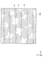
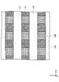
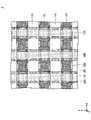
- FIG. 1 is a top view showing a quantum bit circuit according to the first embodiment.
- FIG. 2 is an enlarged view showing a part of FIG. 1.
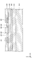
- FIG. 3 is a cross-sectional view (No. 1) showing a quantum bit circuit according to the first embodiment.
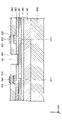
- FIG. 4 is a cross-sectional view (No. 2) showing a quantum bit circuit according to the first embodiment.
- FIG. 5 is a diagram showing an example of the operation of the quantum bit circuit according to the first embodiment.
- FIG. 6 is a top view (No. 1) showing a method of manufacturing a qubit circuit according to the first embodiment.
- FIG. 7 is a top view (No. 2) showing a method of manufacturing a qubit circuit according to the first embodiment.
- FIG. 8 is a top view (No.
- FIG. 9 is a top view (No. 4) showing a method of manufacturing a qubit circuit according to the first embodiment.
- FIG. 10 is a top view (No. 5) showing a method of manufacturing a qubit circuit according to the first embodiment.
- FIG. 11 is a top view (No. 6) showing a method of manufacturing a qubit circuit according to the first embodiment.
- FIG. 12 is a top view (No. 7) showing a method of manufacturing a qubit circuit according to the first embodiment.
- FIG. 13 is a top view (No. 8) showing a method of manufacturing a qubit circuit according to the first embodiment.
- FIG. 14 is a top view showing a quantum bit circuit according to the second embodiment.
- FIG. 15 is an enlarged view showing a part of FIG. 14.
- FIG. 16 is a cross-sectional view (No. 1) showing a quantum bit circuit according to the second embodiment.
- FIG. 17 is a cross-sectional view (No. 2) showing a quantum bit circuit according to the second embodiment.
- FIG. 18 is a band diagram showing an example of the valence band and the conduction band of the laminated body.
- FIG. 19 is a diagram showing changes in the tunnel barrier.
- FIG. 20 is a diagram showing an example of the operation of the quantum bit circuit according to the second embodiment.
- FIG. 21 is a diagram showing a method for manufacturing a qubit circuit according to a second embodiment (No. 1).
- FIG. 22 is a diagram showing a manufacturing method (No. 2) of the quantum bit circuit according to the second embodiment.
- FIG. 23 is a diagram showing a manufacturing method (No. 3) of the qubit circuit according to the second embodiment.
- FIG. 24 is a diagram showing a manufacturing method (No. 4) of the qubit circuit according to the second embodiment.
- FIG. 25 is a diagram showing a method for manufacturing a qubit circuit according to a second embodiment (No. 5).
- FIG. 26 is a diagram showing a method for manufacturing a qubit circuit according to a second embodiment (No. 6).
- FIG. 27 is a diagram showing a manufacturing method (No. 7) of the quantum bit circuit according to the second embodiment.
- FIG. 28 is a diagram showing a method for manufacturing a qubit circuit according to a second embodiment (No. 8).
- FIG. 29 is a diagram showing a method for manufacturing a qubit circuit according to a second embodiment (No. 9).
- FIG. 30 is a top view showing a quantum bit circuit according to the third embodiment with a partial perspective.
- FIG. 31 is a cross-sectional view (No. 1) showing a quantum bit circuit according to the third embodiment.
- FIG. 32 is a cross-sectional view (No. 2) showing the quantum bit circuit according to the third embodiment.
- FIG. 33 is a cross-sectional view (No. 3) showing the quantum bit circuit according to the third embodiment.
- FIG. 34 is a cross-sectional view (No. 4) showing the quantum bit circuit according to the third embodiment.
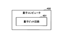
- FIG. 35 is a diagram showing a quantum computer.
- FIG. 1 is a top view showing a quantum bit circuit according to the first embodiment.
- FIG. 2 is an enlarged view showing a part of FIG. 1.
- 3 and 4 are cross-sectional views showing a qubit circuit according to the first embodiment.
- FIG. 3 corresponds to a cross-sectional view taken along line III-III in FIG.
- FIG. 4 corresponds to a cross-sectional view taken along line IV-IV in FIG.
- the quantum bit circuit 1 has a substrate 110, a lower mayorana carrier 121 extending in the X-axis direction, and an upper mayorana carrier 122 extending in the Y-axis direction.
- the substrate 110 is an insulating substrate such as an alumina substrate or a sapphire substrate.
- the X-axis direction and the Y-axis direction are directions orthogonal to the Z-axis direction perpendicular to the surface of the substrate 110.
- the Y-axis direction intersects the X-axis direction, and for example, the X-axis direction and the Y-axis direction are orthogonal to each other. In the present disclosure, viewing an object from the Z-axis direction may be referred to as a plan view.
- the X-axis direction is an example of the first direction
- the Y-axis direction is an example of the second direction.
- the lower Majorana carrier 121 is, for example, a two-dimensional topological insulator layer having a first edge 161 and a third edge 163 extending in the X-axis direction.
- the first edge 161 is located on the ⁇ Y side of the third edge 163.
- the lower Majorana carrier 121 may be composed of a single two-dimensional topological insulator, or may be configured by laminating a plurality of two-dimensional topological insulators.
- the material of the lower Mayorana carrier 121 is, for example, tungsten diterrudate (WTe 2 ). In this embodiment, a plurality of lower Mayorana carriers 121 are arranged side by side in the Y-axis direction.
- the lower Mayorana carrier 121 is an example of the first Mayorana carrier.
- the upper Majorana carrier 122 is, for example, a two-dimensional topological insulator layer having a second edge 162 and a fourth edge 164 extending in the Y-axis direction.
- the second edge 162 is located on the ⁇ X side of the fourth edge 164.
- the upper Majorana carrier 122 may be composed of a single two-dimensional topological insulator, or may be configured by laminating a plurality of two-dimensional topological insulators.
- the material of the upper Mayorana carrier 122 is, for example, tungsten ditelludate (WTe 2 ). In this embodiment, a plurality of upper Mayorana carriers 122 are arranged side by side in the X-axis direction.
- the upper Mayorana carrier 122 is an example of a second Mayorana carrier.
- a lower s wave superconductor layer 131 in contact with the lower surface of the lower Majorana carrier 121 is provided.
- the lower s-wave superconductor layer 131 is provided along the first edge 161 and the third edge 163 for each region overlapping the upper Majorana carrier 122 in a plan view.
- the X-axis end of each lower s wave superconductor layer 131 is separated from the second edge 162 and the fourth edge 164 of the upper Majorana carrier 122 in plan view.
- the lower s wave superconductor layer 131 is, for example, an Al layer.
- a lower s wave superconductor layer 132 in contact with the upper surface of the lower Majorana carrier 121 is provided.
- the lower s-wave superconductor layer 132 is provided along the first edge 161 and the third edge 163 for each region between the upper Majorana carriers 122 adjacent to each other in a plan view.
- the X-axis end of each lower s wave superconductor layer 132 is separated from the second edge 162 and the fourth edge 164 of the upper Majorana carrier 122 in plan view.
- the lower s wave superconductor layer 132 is, for example, an Al layer.
- the lower s-wave superconductor layers 131 and 132 are examples of the first s-wave superconductor layer.
- An upper s wave superconductor layer 133 in contact with the upper surface of the upper Majorana carrier 122 is provided.
- the upper s-wave superconductor layer 133 is provided along the second edge 162 and the fourth edge 164 for each region overlapping the lower majorana carrier 121 and between adjacent lower majorana carriers 121 in a plan view. There is.
- the X-axis end of the upper s-wave superconductor layer 133 is separated from the first edge 161 and the third edge 163 of the lower Majorana carrier 121 in plan view.
- the upper s wave superconductor layer 133 is, for example, an Al layer.
- the upper s wave superconductor layer 133 is an example of the second s wave superconductor layer.
- An etching stopper 140 is provided between the lower Mayorana carrier 121 and the upper Mayorana carrier 122.
- the material of the etching stopper 140 is, for example, graphene or graphite. When the material of the etching stopper 140 is graphite, the thinner it is, the more preferable it is, and for example, it is preferably 5 nm or less. This is because the Majorana fermions tunnel the etching stopper 140 between the lower Majorana carrier 121 and the upper Majorana carrier 122, as will be described later.
- Wiring is individually connected to the lower s wave superconductor layer 131, the lower s wave superconductor layer 132, and the upper s wave superconductor layer 133.
- Mayorana particles can be present in the portion between the s-wave superconductor layer 131 and the lower s-wave superconductor layer 132.
- the portion overlapping the second edge 162 of the first edge 161 functions as the first region 171 and overlaps with the second edge 162 of the third edge 163. Functions as the third region 173.
- the portion overlapping the fourth edge 164 of the first edge 161 functions as the fifth region 175 and overlaps with the fourth edge 164 of the third edge 163. Functions as the seventh region 177.
- Majorana fermions can be present in the intervening part. Then, for example, among the portions where these Majorana fermions can exist, the portion overlapping the first edge 161 of the second edge 162 functions as the second region 172 and overlaps with the first edge 161 of the fourth edge 164. Functions as the sixth region 176.
- the portion overlapping the third edge 163 of the second edge 162 functions as the fourth region 174, and the portion overlapping the third edge 163 of the fourth edge 164 is the first. It functions as 8 areas 178.
- the Majorana particles existing in the first region 171 and the Majorana particles existing in the second region 172 can pass through the etching stopper 140 by the tunnel effect and interact with each other. Therefore, both Majorana fermions can be regarded as a single Majorana fermion. The same applies to the pair of the third region 173 and the fourth region 174, the pair of the fifth region 175 and the sixth region 176, and the pair of the seventh region 177 and the eighth region 178.
- the Majorana fermion generated on the lower Majorana carrier 121 and the Majorana fermion generated on the upper Majorana carrier 122 can be easily interacted with each other. Further, as will be described later, such a structure can be manufactured with a high yield if the alignment accuracy in the conventional semiconductor process is obtained.
- the Mayorana qubits can be integrated at high density.
- the Mayorana qubits can be regularly integrated in a grid pattern, making it easy to design wiring and the like.
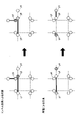
- FIG. 5 is a diagram showing an example of the operation of the quantum bit circuit according to the first embodiment.
- the circles in FIG. 5 indicate the Majorana fermions in regions 171 to 178.
- the line segment shown by the broken line indicates that the s-wave superconductor layer is in a state where the Majorana fermion cannot be exchanged, and the line segment shown by the solid line. Indicates that the s-wave superconductor layer is ready for the exchange of Majorana fermions.
- the Majorana fermion is exchanged between two adjacent fifth regions 175 with the first region 171 in the X-axis direction. That is, the Majorana particles ⁇ 1 generated in one fifth region 175 and the Majorana particles ⁇ 4 generated in the other fifth region 175 are exchanged by charging via the Majorana particles ⁇ 2 generated in the first region 171 between them. do.
- 6 to 13 are top views showing a method of manufacturing a qubit circuit according to the first embodiment.
- the lower s wave superconductor layer 131 is formed on the substrate 110.
- the lower s wave superconductor layer 131 can be formed, for example, by a vapor deposition method.
- a two-dimensional topological insulator layer 121X is provided on the substrate 110 so as to cover the lower s wave superconductor layer 131.
- the two-dimensional topological insulator layer 121X can be provided, for example, by separately growing it on a growth substrate (not shown) and transferring it from the growth substrate.
- the two-dimensional topological insulator layer 121X may be formed on the substrate 110.
- a plurality of lower Majorana carriers 121 are formed by processing the two-dimensional topological insulator layer 121X.
- RIE reactive ion etching
- the etching gas for example, a fluorocarbon gas is used.
- an etching stopper 140X is provided above the substrate 110 so as to cover the lower Mayorana carrier 121.
- the etching stopper 140X can be provided, for example, by separately growing it on a growth substrate (not shown) and transferring it from the growth substrate.
- a two-dimensional topological insulator layer 122X is provided on the etching stopper 140X.
- the two-dimensional topological insulator layer 122X can be provided, for example, by separately growing it on a growth substrate (not shown) and transferring it from the growth substrate.
- the two-dimensional topological insulator layer 122X may be formed on the etching stopper 140X.
- a plurality of upper Majorana carriers 122 are formed by processing the two-dimensional topological insulator layer 122X.
- RIE is performed in the processing of the two-dimensional topological insulator layer 122X.
- the etching gas for example, a fluorocarbon gas is used.
- the lower Mayorana carrier 121 is protected by the etching stopper 140X.
- the etching stopper 140X is formed between the lower Mayorana carrier 121 and the upper Mayorana carrier 122.
- the processing of the etching stopper 140X for example, RIE is performed.
- the etching gas for example, oxygen gas is used.
- the lower s wave superconductor layer 132 is formed on the lower Majorana carrier 121, and the upper s wave superconductor layer 133 is formed on the upper Majorana carrier 122.
- the lower s wave superconductor layer 132 and the upper s wave superconductor layer 133 can be formed, for example, by a vapor deposition method.
- the qubit circuit 1 according to the first embodiment can be manufactured.
- the qubit circuit 1 can be manufactured with a high yield if there is alignment accuracy in the conventional semiconductor process.
- Both the lower s wave superconductor layer 131 and the lower s wave superconductor layer 132 may be in contact with the lower surface of the lower Mayorana carrier 121, and the lower s wave superconductor layer 131 and the lower s wave superconductor layer 131 may be in contact with the lower surface. Both layers 132 may be in contact with the upper surface of the lower Mayorana carrier 121.
- FIG. 14 is a top view showing a quantum bit circuit according to the second embodiment.
- FIG. 15 is an enlarged view showing a part of FIG. 14.
- 16 and 17 are cross-sectional views showing a quantum bit circuit according to the second embodiment.
- FIG. 16 corresponds to a cross-sectional view taken along the line XVI-XVI in FIG.
- FIG. 17 corresponds to a cross-sectional view taken along line XVII-XVII in FIG.
- the qubit circuit 2 has a substrate 110, a lower Majorana carrier 121, an upper Majorana carrier 122, a lower s wave superconductor layer 131, and a lower s wave superconductor, as in the first embodiment. It has a conductor layer 132 and an upper s wave superconductor layer 133.
- an etching stopper 241, an etching stopper 242, and a semiconductor layer 250 are provided between the lower Mayorana carrier 121 and the upper Mayorana carrier 122 in place of the etching stopper 140.
- An etching stopper 241 is provided between the lower Mayorana carrier 121 and the semiconductor layer 250, and an etching stopper 242 is provided between the semiconductor layer 250 and the upper Mayorana carrier 122.
- the material of the etching stoppers 241 and 242 is, for example, graphene or graphite.
- the thinner the thickness the more preferable, for example, 5 nm or less. This is because the Majorana fermions tunnel the etching stoppers 241 and 242 between the lower Majorana carrier 121 and the upper Majorana carrier 122.
- the material of the semiconductor layer 250 is a two-dimensional semiconductor such as tin selenide (SnSe 2 ).
- the conductive type of the semiconductor layer 250 is not limited, and may be, for example, an intrinsic semiconductor or an n-type semiconductor.
- the semiconductor layer 250 may be composed of a single two-dimensional semiconductor, or may be configured by laminating a plurality of two-dimensional semiconductors.
- the semiconductor layer 250 is an example of a tunnel barrier layer.
- the lower electrode 251 is provided between the lower s wave superconductor layers 131 adjacent to each other in the X-axis direction.
- the lower electrode 251 is covered with the lower Majorana carrier 121, similarly to the lower s-wave superconductor layer 131.
- the lower electrode 251 is provided in a region that does not overlap with the upper Mayorana carrier 122 in a plan view.
- the lower electrode 251 is provided, for example, in the vicinity of the first region 171, the vicinity of the third region 173, the vicinity of the fifth region 175, and the vicinity of the seventh region 177, respectively.
- the upper electrode 252 is provided on the upper Mayorana carrier 122.
- the upper electrode 252 is provided, for example, in the vicinity of the second region 172, the vicinity of the fourth region 174, the vicinity of the sixth region 176, and the vicinity of the eighth region 178, respectively.
- a power supply 253 for applying a voltage is provided between the lower electrode 251 and the upper electrode 252 provided in the vicinity of the first region 171 and the second region 172 that overlap each other.
- Another power supply 253 that applies a voltage between the lower electrode 251 and the upper electrode 252 provided in the vicinity of the third region 173 and the fourth region 174 that overlap each other is also provided.
- Another power supply 253 that applies a voltage between the lower electrode 251 and the upper electrode 252 provided in the vicinity of the fifth region 175 and the sixth region 176 that overlap each other is also provided.
- Another power supply 253 that applies a voltage between the lower electrode 251 and the upper electrode 252 provided in the vicinity of the seventh region 177 and the eighth region 178 that overlap each other is also provided.
- FIG. 18 shows an example of a band diagram of a valence band and a conduction band of a laminate of a lower Mayorana carrier 121, an etching stopper 241 and a semiconductor layer 250, an etching stopper 242, and an upper Mayorana carrier 122.
- FIG. 18 shows an example of a band diagram of a valence band and a conduction band of a laminate of a lower Mayorana carrier 121, an etching stopper 241 and a semiconductor layer 250, an etching stopper 242, and an upper Mayorana carrier 122.
- the lower Mayorana carrier 121 and the upper Mayorana carrier 122 are each composed of a single WTe 2
- the etching stoppers 241 and 242 are composed of graphene
- the semiconductor layer 250 is composed of four layers of SnSe 2 . ing.
- the semiconductor layer 250 Since the semiconductor layer 250 is provided, there is a tunnel barrier between the Majorana fermion generated on the lower Majorana carrier 121 and the Majorana fermion generated on the upper Majorana carrier 122.
- the height of this tunnel barrier can be adjusted by the magnitude of the gate voltage applied from the power supply 253. For example, by applying a gate voltage, the band of the semiconductor layer 250 can be changed, the tunnel barrier can be lowered, and the tunnel effect can be induced.
- FIG. 19 is a diagram showing changes in the tunnel barrier.
- FIG. 19 shows changes in the valence band EV and the conduction band EC of the semiconductor layer 250 together with the Fermi level E F.
- the resonance tunnel effect can be exhibited by applying the gate voltage VG .
- the tunnel effect allows the Majorana fermion to move back and forth between the two states. Therefore, by restoring the tunnel barrier at a desired timing, for example, the Majorana particles ⁇ 2 generated in the first region 171 can be exchanged with the Majorana particles ⁇ 5 generated in the second region 172. That is, the quantum gate operation can be performed.
- FIG. 20 is a diagram showing an example of the operation of the quantum bit circuit according to the second embodiment. Similar to FIG. 5, circles in FIG. 20 indicate Majorana fermions in regions 171-178. Of the line segments connecting the two Majorana fermions, the line segment shown by the broken line indicates that the s-wave superconductor layer is in a state where the Majorana fermion cannot be exchanged, and the line segment shown by the solid line. Indicates that the s-wave superconductor layer is ready for the exchange of Majorana fermions.
- the Majorana fermion can be exchanged by charging, whereas in the qubit circuit 2 according to the second embodiment, in addition to the exchange of Majorana particles by charging, the gate voltage can be exchanged. It is possible to exchange Majorana fermions by the tunnel effect through the control of.
- the Majorana fermion is exchanged between the first region 171 and the second region 172 by applying the gate voltage VG . That is, the Majorana particles ⁇ 2 generated in the first region 171 and the Majorana particles generated in the second region 172 are exchanged through the tunnel of the semiconductor layer 250.
- the Majorana fermion is exchanged between two adjacent fifth regions 175 with the first region 171 sandwiched in the X-axis direction. That is, the Majorana particles ⁇ 1 generated in one fifth region 175 and the Majorana particles ⁇ 4 generated in the other fifth region 175 are exchanged by charging via the Majorana particles ⁇ 2 generated in the first region 171 between them. do.
- 21 to 29 are diagrams showing a method of manufacturing a qubit circuit according to a second embodiment.
- the lower s wave superconductor layer 131 is formed on the substrate 110 in the same manner as in the first embodiment.
- the lower s wave superconductor layer 131 can be formed, for example, by a vapor deposition method.
- the lower electrode 251 is formed on the substrate 110.
- the lower electrode 251 can be formed, for example, by a vapor deposition method.
- a plurality of lower Mayorana carriers 121 are formed in the same manner as in the first embodiment.
- an etching stopper 241X is provided on the substrate 110 so as to cover the lower Mayorana carrier 121.
- the etching stopper 241X can be provided, for example, by separately growing it on a growth substrate (not shown) and transferring it from the growth substrate.
- the etching stopper 241X is an example of the first etching stopper.
- a semiconductor layer 250X is provided on the etching stopper 241X.
- the semiconductor layer 250X can be provided, for example, by separately growing it on a growth substrate (not shown) and transferring it from the growth substrate.
- a plurality of semiconductor layers 250 are formed by processing the semiconductor layer 250X.
- RIE is performed.
- the etching gas for example, a fluorocarbon gas is used.
- the lower Mayorana carrier 121 is protected by the etching stopper 241X.
- the etching stopper 241X is processed to form the etching stopper 241 between the lower Mayorana carrier 121 and the semiconductor layer 250.
- the processing of the etching stopper 241X for example, RIE is performed.
- the etching gas for example, oxygen gas is used.
- an etching stopper 242X is provided above the substrate 110 so as to cover the lower Mayorana carrier 121 and the semiconductor layer 250.
- the etching stopper 242X can be provided, for example, by separately growing it on a growth substrate (not shown) and transferring it from the growth substrate.
- the etching stopper 242X is an example of a second etching stopper.
- a two-dimensional topological insulator layer 122X is provided on the etching stopper 242X.
- the two-dimensional topological insulator layer 122X can be provided, for example, by separately growing it on a growth substrate (not shown) and transferring it from the growth substrate.
- the two-dimensional topological insulator layer 122X may be formed on the etching stopper 242X.
- a plurality of upper Majorana carriers 122 are formed by processing the two-dimensional topological insulator layer 122X.
- RIE is performed in the processing of the two-dimensional topological insulator layer 122X.
- the etching gas for example, a fluorocarbon gas is used.
- the lower Mayorana carrier 121 is protected by the etching stopper 242X.
- the etching stopper 242X is processed to form the etching stopper 242 between the semiconductor layer 250 and the upper Mayorana carrier 122.
- the processing of the etching stopper 242X for example, RIE is performed.
- the etching gas for example, oxygen gas is used.
- the lower s wave superconductor layer 132 is formed on the lower Majorana carrier 121, and the upper s wave superconductor layer 133 is formed on the upper Majorana carrier 122. Further, an upper electrode 252 is formed on the upper Mayorana carrier 122.
- the upper electrode 252 can be formed, for example, by a vapor deposition method.
- the qubit circuit 2 according to the second embodiment can be manufactured.
- FIG. 30 is a top view showing a quantum bit circuit according to the third embodiment with a partial perspective.
- 31 to 34 are cross-sectional views showing a quantum bit circuit according to a third embodiment.
- FIG. 31 corresponds to a cross-sectional view taken along the line XXXI-XXXI in FIG.
- FIG. 32 corresponds to a cross-sectional view taken along the line XXXII-XXXII in FIG.
- FIG. 33 corresponds to a cross-sectional view taken along the line XXXIII-XXXIII in FIG.
- FIG. 34 corresponds to a cross-sectional view taken along the line XXIV-XXXIV in FIG.
- the qubit circuit 3 has a substrate 310, a lower Mayorana carrier 321 extending in the X-axis direction, and an upper Mayorana carrier 322 extending in the Y-axis direction.
- the substrate 310 is, for example, a semiconductor substrate such as a GaAs substrate or an InP substrate having a surface orientation of (100).
- the X-axis direction and the Y-axis direction are directions orthogonal to the Z-axis direction perpendicular to the surface of the substrate 310.
- the Y-axis direction intersects the X-axis direction, and for example, the X-axis direction and the Y-axis direction are orthogonal to each other.
- the lower Majorana carrier 321 is a semiconductor nanowire made of, for example, InAs.
- a plurality of lower Mayorana carriers 321 are arranged side by side in the Y-axis direction.
- the lower Mayorana carrier 321 is an example of the first Mayorana carrier.
- the upper Majorana carrier 322 is a semiconductor nanowire made of, for example, InAs.
- a plurality of upper Mayorana carriers 122 are arranged side by side in the X-axis direction.
- the upper Mayorana carrier 322 is an example of a second Mayorana carrier.
- a buffer layer 381 and a base semiconductor layer 382 are provided on the substrate 310.
- the buffer layer 381 is an In 1-x Al x As layer having a thickness of about 1 ⁇ m, and is lattice-matched to the substrate 310 and the underlying semiconductor layer 382 from the interface with the substrate 310 to the interface with the underlying semiconductor layer 382.
- the Al composition x may be changed as described above.
- the underlying semiconductor layer 382 is an In 0.81 Ga 0.19 As layer having a thickness of about 4 nm.
- the lower Mayorana carrier 321 is formed on the underlying semiconductor layer 382.
- the thickness of the lower Mayorana carrier 321 is, for example, about 5 nm.
- a barrier layer 383 is formed on the underlying semiconductor layer 382 so as to cover the lower Mayorana carrier 321.
- the barrier layer 383 is an In 0.9 Al 0.1 As layer having a thickness of about 5 nm on the lower Mayorana carrier 321.
- the lower Mayorana carrier 321 is covered with a barrier layer 383 and functions as a quantum well.
- the upper Mayorana carrier 322 is formed on the barrier layer 383.
- the thickness of the upper Mayorana carrier 322 is, for example, about 5 nm.
- a barrier layer 384 is formed on the barrier layer 383 so as to cover the upper Mayorana carrier 322.
- the barrier layer 384 is an In 0.9 Al 0.1 As layer having a thickness of about 5 nm on the upper Mayorana carrier 322.
- the upper Mayorana carrier 322 is covered with a barrier layer 384 and functions as a quantum well.
- an opening 391 reaching the underlying semiconductor layer 382 is formed in the barrier layers 383 and 384 in the vicinity of the lower Mayorana carrier 321 in a plan view, and a lower s wave is formed in the opening 391.
- a superconductor layer 331 is provided.
- the lower s wave superconductor layer 331 is, for example, an Al layer.
- the lower s wave superconductor layer 331 is an example of the first s wave superconductor layer.
- an opening 392 reaching the barrier layer 383 is formed in the barrier layer 384 in the vicinity of the upper Mayorana carrier 322 in a plan view, and an upper s wave superconductor is formed in the opening 392.
- a layer 332 is provided.
- the upper s wave superconductor layer 332 is, for example, an Al layer.
- the upper s wave superconductor layer 332 is an example of the second s wave superconductor layer.
- an opening 393 reaching the lower Mayorana carrier 321 is formed in the barrier layers 383 and 384, and a lower electrode 351 is formed in the opening 393.
- the upper electrode 352 is formed on the barrier layer 384 in the region where the lower Mayorana carrier 321 and the upper Mayorana carrier 322 overlap in a plan view.
- a power supply 353 for applying a voltage is provided between one lower electrode 351 and one upper electrode 352 adjacent to each other in the X direction. The power supply 353 is provided for each set of the lower electrode 351 and the upper electrode 352.
- majorana fermions can be present in a portion of the lower Majorana carrier 321 that overlaps with the upper Majorana carrier 322 in plan view and a portion of the upper Majorana carrier 322 that overlaps with the lower Majorana carrier 321 in plan view. Then, for example, among the portions where these Majorana fermions can exist, the portion overlapping the upper Majorana carrier 322 in the plan view of the lower Majorana carrier 321 functions as the first region 371, and the lower portion in the plan view of the upper Majorana carrier 322. The portion overlapping the Majorana carrier 321 functions as the second region 372.
- the Majorana fermion can be exchanged between two first regions 371 adjacent to each other in the X-axis direction.
- the state of the upper s wave superconductor layer 332 Majorana fermions can be exchanged between two second regions 372 adjacent to each other in the Y-axis direction.
- the gate voltage applied from the power supply 353 the Majorana fermion can be exchanged between the first region 371 and the second region 372 that are adjacent to each other in the Z-axis direction.
- the qubit circuits 1, 2 and 3 can be used, for example, as a qubit circuit 401 by being incorporated in a quantum computer 400.
- Qubit circuit 110 Substrate 121, 321: Lower majorana carrier 122, 322: Upper majorana carrier 131, 132, 331: Lower s-wave superconductor layer 133, 332: Upper s-wave superconductivity Body layer 140, 241 and 242: Etching stopper 161 to 164: Edge 171 to 178, 371, 372: Region 250: Semiconductor layer 251, 351: Lower electrode 252, 352: Upper electrode 253, 353: Power supply 400: Quantum computer
Landscapes
- Engineering & Computer Science (AREA)
- Manufacturing & Machinery (AREA)
- General Physics & Mathematics (AREA)
- Physics & Mathematics (AREA)
- Theoretical Computer Science (AREA)
- Computational Mathematics (AREA)
- Computing Systems (AREA)
- Evolutionary Computation (AREA)
- Condensed Matter Physics & Semiconductors (AREA)
- Mathematical Analysis (AREA)
- Mathematical Optimization (AREA)
- Pure & Applied Mathematics (AREA)
- Data Mining & Analysis (AREA)
- General Engineering & Computer Science (AREA)
- Mathematical Physics (AREA)
- Software Systems (AREA)
- Artificial Intelligence (AREA)
- Superconductor Devices And Manufacturing Methods Thereof (AREA)
- Semiconductor Memories (AREA)
Priority Applications (5)
| Application Number | Priority Date | Filing Date | Title |
|---|---|---|---|
| JP2022570877A JPWO2022137421A1 (https=) | 2020-12-24 | 2020-12-24 | |
| EP20966910.0A EP4270502A4 (en) | 2020-12-24 | 2020-12-24 | Quantum bit circuit, quantum bit computer, and quantum bit circuit manufacturing method |
| PCT/JP2020/048426 WO2022137421A1 (ja) | 2020-12-24 | 2020-12-24 | 量子ビット回路、量子コンピュータ及び量子ビット回路の製造方法 |
| CN202080107411.4A CN116472612A (zh) | 2020-12-24 | 2020-12-24 | 量子比特电路、量子计算机以及量子比特电路的制造方法 |
| US18/311,261 US20230329126A1 (en) | 2020-12-24 | 2023-05-03 | Quantum bit circuit, quantum computer, method for manufacturing quantum bit circuit |
Applications Claiming Priority (1)
| Application Number | Priority Date | Filing Date | Title |
|---|---|---|---|
| PCT/JP2020/048426 WO2022137421A1 (ja) | 2020-12-24 | 2020-12-24 | 量子ビット回路、量子コンピュータ及び量子ビット回路の製造方法 |
Related Child Applications (1)
| Application Number | Title | Priority Date | Filing Date |
|---|---|---|---|
| US18/311,261 Continuation US20230329126A1 (en) | 2020-12-24 | 2023-05-03 | Quantum bit circuit, quantum computer, method for manufacturing quantum bit circuit |
Publications (1)
| Publication Number | Publication Date |
|---|---|
| WO2022137421A1 true WO2022137421A1 (ja) | 2022-06-30 |
Family
ID=82159171
Family Applications (1)
| Application Number | Title | Priority Date | Filing Date |
|---|---|---|---|
| PCT/JP2020/048426 Ceased WO2022137421A1 (ja) | 2020-12-24 | 2020-12-24 | 量子ビット回路、量子コンピュータ及び量子ビット回路の製造方法 |
Country Status (5)
| Country | Link |
|---|---|
| US (1) | US20230329126A1 (https=) |
| EP (1) | EP4270502A4 (https=) |
| JP (1) | JPWO2022137421A1 (https=) |
| CN (1) | CN116472612A (https=) |
| WO (1) | WO2022137421A1 (https=) |
Cited By (4)
| Publication number | Priority date | Publication date | Assignee | Title |
|---|---|---|---|---|
| JPWO2024023967A1 (https=) * | 2022-07-27 | 2024-02-01 | ||
| JPWO2024047817A1 (https=) * | 2022-08-31 | 2024-03-07 | ||
| WO2024127469A1 (ja) * | 2022-12-12 | 2024-06-20 | 富士通株式会社 | 積層構造体、量子ビットデバイス、積層構造体の製造方法及び量子ビットデバイスの製造方法 |
| WO2024150293A1 (ja) * | 2023-01-11 | 2024-07-18 | 富士通株式会社 | 量子変換器及び量子変換方法 |
Citations (5)
| Publication number | Priority date | Publication date | Assignee | Title |
|---|---|---|---|---|
| JP2013247267A (ja) | 2012-05-28 | 2013-12-09 | National Institute For Materials Science | 縁マヨラナフェルミ粒子を使用したトポロジカル量子計算用デバイスユニット、及びその操作方法、並びにトポロジカル量子計算用デバイス、及びその操作方法 |
| US20140279822A1 (en) * | 2013-03-15 | 2014-09-18 | Microsoft Corporation | Topological Quantum Computation via Tunable Interactions |
| US20180052806A1 (en) * | 2016-08-17 | 2018-02-22 | Microsof Technology Licensing, LLC | Quantum computing methods and devices for majorana tetron qubits |
| US20190013457A1 (en) * | 2017-07-07 | 2019-01-10 | Microsoft Technology Licensing, Llc | Use of selective hydrogen etching technique for building topological qubits |
| JP2020511780A (ja) | 2017-03-20 | 2020-04-16 | フォルシュングスツェントルム・ユーリッヒ・ゲゼルシャフト・ミット・ベシュレンクテル・ハフツング | マヨラナ材料と超伝導体のハイブリッド網構造のインサイチュによる製造方法及びその方法により製造されたハイブリッド構造 |
Family Cites Families (8)
| Publication number | Priority date | Publication date | Assignee | Title |
|---|---|---|---|---|
| US9040959B2 (en) * | 2012-05-08 | 2015-05-26 | Microsoft Technology Licensing, Llc | Multi-band topological nanowires |
| US10333048B2 (en) * | 2015-09-20 | 2019-06-25 | Microsoft Technology Licensing, Llc | Universal topological quantum computers based on majorana nanowire networks |
| WO2018035361A1 (en) * | 2016-08-17 | 2018-02-22 | Microsoft Technology Licensing, Llc | Quantum computing methods and devices for majorana qubits |
| US10490600B2 (en) * | 2016-08-17 | 2019-11-26 | Microsoft Technology Licensing, Llc | Quantum computing devices with majorana hexon qubits |
| EP3695351B1 (en) * | 2017-11-19 | 2024-07-24 | Microsoft Technology Licensing, LLC | Quantum spin hall-based charging energy-protected quantum computation |
| WO2019140031A2 (en) * | 2018-01-10 | 2019-07-18 | Massachusetts Institute Of Technology | Quantum information processing with majorana bound states in superconducting circuits |
| US10692010B2 (en) * | 2018-07-20 | 2020-06-23 | Microsoft Technology Licensing, Llc | Form and fabrication of semiconductor-superconductor nanowires and quantum devices based thereon |
| US11100419B2 (en) * | 2019-05-06 | 2021-08-24 | Massachusetts Institute Of Technology | Majorana pair based qubits for fault tolerant quantum computing architecture using superconducting gold surface states |
-
2020
- 2020-12-24 CN CN202080107411.4A patent/CN116472612A/zh active Pending
- 2020-12-24 WO PCT/JP2020/048426 patent/WO2022137421A1/ja not_active Ceased
- 2020-12-24 JP JP2022570877A patent/JPWO2022137421A1/ja active Pending
- 2020-12-24 EP EP20966910.0A patent/EP4270502A4/en not_active Withdrawn
-
2023
- 2023-05-03 US US18/311,261 patent/US20230329126A1/en active Pending
Patent Citations (5)
| Publication number | Priority date | Publication date | Assignee | Title |
|---|---|---|---|---|
| JP2013247267A (ja) | 2012-05-28 | 2013-12-09 | National Institute For Materials Science | 縁マヨラナフェルミ粒子を使用したトポロジカル量子計算用デバイスユニット、及びその操作方法、並びにトポロジカル量子計算用デバイス、及びその操作方法 |
| US20140279822A1 (en) * | 2013-03-15 | 2014-09-18 | Microsoft Corporation | Topological Quantum Computation via Tunable Interactions |
| US20180052806A1 (en) * | 2016-08-17 | 2018-02-22 | Microsof Technology Licensing, LLC | Quantum computing methods and devices for majorana tetron qubits |
| JP2020511780A (ja) | 2017-03-20 | 2020-04-16 | フォルシュングスツェントルム・ユーリッヒ・ゲゼルシャフト・ミット・ベシュレンクテル・ハフツング | マヨラナ材料と超伝導体のハイブリッド網構造のインサイチュによる製造方法及びその方法により製造されたハイブリッド構造 |
| US20190013457A1 (en) * | 2017-07-07 | 2019-01-10 | Microsoft Technology Licensing, Llc | Use of selective hydrogen etching technique for building topological qubits |
Non-Patent Citations (4)
| Title |
|---|
| "Coulomb-assisted braiding of Majorana fermions in a Josephson junction array", NEW JOURNAL OF PHYSICS, vol. 14, pages 035019 |
| "Direct visualization of a two-dimensional topological insulator in the single-layer 1T'-WTe2", PHYSICAL REVIEW B, vol. 96, 2017 |
| "Minimal circuit for a flux-controlled Majorana qubit in a quantum spin-Hall insulator", PHYSICA SCRIPTA, vol. T164, pages 014007 |
| See also references of EP4270502A4 |
Cited By (5)
| Publication number | Priority date | Publication date | Assignee | Title |
|---|---|---|---|---|
| JPWO2024023967A1 (https=) * | 2022-07-27 | 2024-02-01 | ||
| WO2024023967A1 (ja) * | 2022-07-27 | 2024-02-01 | 富士通株式会社 | 構造体、量子ビット、量子演算装置及び構造体の製造方法 |
| JPWO2024047817A1 (https=) * | 2022-08-31 | 2024-03-07 | ||
| WO2024127469A1 (ja) * | 2022-12-12 | 2024-06-20 | 富士通株式会社 | 積層構造体、量子ビットデバイス、積層構造体の製造方法及び量子ビットデバイスの製造方法 |
| WO2024150293A1 (ja) * | 2023-01-11 | 2024-07-18 | 富士通株式会社 | 量子変換器及び量子変換方法 |
Also Published As
| Publication number | Publication date |
|---|---|
| EP4270502A1 (en) | 2023-11-01 |
| EP4270502A4 (en) | 2024-02-14 |
| CN116472612A (zh) | 2023-07-21 |
| US20230329126A1 (en) | 2023-10-12 |
| JPWO2022137421A1 (https=) | 2022-06-30 |
Similar Documents
| Publication | Publication Date | Title |
|---|---|---|
| WO2022137421A1 (ja) | 量子ビット回路、量子コンピュータ及び量子ビット回路の製造方法 | |
| US20210336119A1 (en) | Use of selective hydrogen etching technique for building topological qubits | |
| JP4669957B2 (ja) | グラフェンを用いる半導体装置及びその製造方法 | |
| US11707000B2 (en) | Side-gating in selective-area-grown topological qubits | |
| JP7532382B2 (ja) | 量子デバイスの製作 | |
| KR102216543B1 (ko) | 그래핀-금속 접합 구조체 및 그 제조방법, 그래핀-금속 접합 구조체를 구비하는 반도체 소자 | |
| US20230031861A1 (en) | Transistor including two-dimensional (2d) channel | |
| JPWO2022137421A5 (https=) | ||
| WO2019107411A1 (ja) | トンネル電界効果トランジスタ | |
| JP2018198310A (ja) | 半導体部品 | |
| EP2401764A1 (en) | Method for manufacturing nano electronic devices made from 2d carbon crystals like graphene and devices obtained with this method | |
| US20240306518A1 (en) | Structure, quantum bit, and method for manufacturing structure | |
| JP7666617B2 (ja) | 量子ビット、量子演算装置及び量子ビットの製造方法 | |
| JP7679884B2 (ja) | マヨラナ量子ビット及び量子コンピュータ | |
| JP7698225B2 (ja) | トポロジカル絶縁体、量子ビット、トポロジカル絶縁体の製造方法、および量子ビットの製造方法 | |
| Pang et al. | A novel spin-valley-coupled nodal-ring semimetal in single-layer Ta 2 C 3 | |
| WO2023132045A1 (ja) | 量子デバイス及び量子デバイスの制御方法 | |
| CN115362553A (zh) | 制造栅极的方法 | |
| KR20260020106A (ko) | 트랜지스터 및 그 제조 방법, 그리고 집적 회로 | |
| Soliman et al. | Theoretical study on the quantum well junction CrI3/CrGeTe3 | |
| US20240420003A1 (en) | Tapered nanowire device for quantum computing | |
| KR102130220B1 (ko) | 이종 계면을 갖는 열전 구조체 및 이를 포함하는 열전 소자 | |
| Yang et al. | Designing double isolated bands and subgap states in two-dimensional X PS 3 (X= Al, Ga, In, Tl) for achieving bi-anti-ambipolar transport | |
| JP6621498B2 (ja) | 半導体構造及び半導体部品 | |
| WO2023223531A1 (ja) | 量子デバイス及び量子デバイスの製造方法 |
Legal Events
| Date | Code | Title | Description |
|---|---|---|---|
| 121 | Ep: the epo has been informed by wipo that ep was designated in this application |
Ref document number: 20966910 Country of ref document: EP Kind code of ref document: A1 |
|
| WWE | Wipo information: entry into national phase |
Ref document number: 202080107411.4 Country of ref document: CN |
|
| ENP | Entry into the national phase |
Ref document number: 2022570877 Country of ref document: JP Kind code of ref document: A |
|
| NENP | Non-entry into the national phase |
Ref country code: DE |
|
| ENP | Entry into the national phase |
Ref document number: 2020966910 Country of ref document: EP Effective date: 20230724 |