WO2022130953A1 - 膜付き透明基板及び調理器用トッププレート - Google Patents
膜付き透明基板及び調理器用トッププレート Download PDFInfo
- Publication number
- WO2022130953A1 WO2022130953A1 PCT/JP2021/043656 JP2021043656W WO2022130953A1 WO 2022130953 A1 WO2022130953 A1 WO 2022130953A1 JP 2021043656 W JP2021043656 W JP 2021043656W WO 2022130953 A1 WO2022130953 A1 WO 2022130953A1
- Authority
- WO
- WIPO (PCT)
- Prior art keywords
- film
- transparent substrate
- light
- refractive index
- light absorption
- Prior art date
- Legal status (The legal status is an assumption and is not a legal conclusion. Google has not performed a legal analysis and makes no representation as to the accuracy of the status listed.)
- Ceased
Links
Images





Classifications
-
- C—CHEMISTRY; METALLURGY
- C03—GLASS; MINERAL OR SLAG WOOL
- C03C—CHEMICAL COMPOSITION OF GLASSES, GLAZES OR VITREOUS ENAMELS; SURFACE TREATMENT OF GLASS; SURFACE TREATMENT OF FIBRES OR FILAMENTS MADE FROM GLASS, MINERALS OR SLAGS; JOINING GLASS TO GLASS OR OTHER MATERIALS
- C03C17/00—Surface treatment of glass, not in the form of fibres or filaments, by coating
- C03C17/22—Surface treatment of glass, not in the form of fibres or filaments, by coating with other inorganic material
- C03C17/23—Oxides
- C03C17/245—Oxides by deposition from the vapour phase
-
- C—CHEMISTRY; METALLURGY
- C03—GLASS; MINERAL OR SLAG WOOL
- C03C—CHEMICAL COMPOSITION OF GLASSES, GLAZES OR VITREOUS ENAMELS; SURFACE TREATMENT OF GLASS; SURFACE TREATMENT OF FIBRES OR FILAMENTS MADE FROM GLASS, MINERALS OR SLAGS; JOINING GLASS TO GLASS OR OTHER MATERIALS
- C03C17/00—Surface treatment of glass, not in the form of fibres or filaments, by coating
- C03C17/34—Surface treatment of glass, not in the form of fibres or filaments, by coating with at least two coatings having different compositions
- C03C17/3411—Surface treatment of glass, not in the form of fibres or filaments, by coating with at least two coatings having different compositions with at least two coatings of inorganic materials
- C03C17/3417—Surface treatment of glass, not in the form of fibres or filaments, by coating with at least two coatings having different compositions with at least two coatings of inorganic materials all coatings being oxide coatings
-
- C—CHEMISTRY; METALLURGY
- C03—GLASS; MINERAL OR SLAG WOOL
- C03C—CHEMICAL COMPOSITION OF GLASSES, GLAZES OR VITREOUS ENAMELS; SURFACE TREATMENT OF GLASS; SURFACE TREATMENT OF FIBRES OR FILAMENTS MADE FROM GLASS, MINERALS OR SLAGS; JOINING GLASS TO GLASS OR OTHER MATERIALS
- C03C17/00—Surface treatment of glass, not in the form of fibres or filaments, by coating
- C03C17/34—Surface treatment of glass, not in the form of fibres or filaments, by coating with at least two coatings having different compositions
- C03C17/3411—Surface treatment of glass, not in the form of fibres or filaments, by coating with at least two coatings having different compositions with at least two coatings of inorganic materials
- C03C17/3429—Surface treatment of glass, not in the form of fibres or filaments, by coating with at least two coatings having different compositions with at least two coatings of inorganic materials at least one of the coatings being a non-oxide coating
- C03C17/3435—Surface treatment of glass, not in the form of fibres or filaments, by coating with at least two coatings having different compositions with at least two coatings of inorganic materials at least one of the coatings being a non-oxide coating comprising a nitride, oxynitride, boronitride or carbonitride
-
- F—MECHANICAL ENGINEERING; LIGHTING; HEATING; WEAPONS; BLASTING
- F24—HEATING; RANGES; VENTILATING
- F24C—DOMESTIC STOVES OR RANGES ; DETAILS OF DOMESTIC STOVES OR RANGES, OF GENERAL APPLICATION
- F24C15/00—Details
- F24C15/10—Tops, e.g. hot plates; Rings
-
- H—ELECTRICITY
- H05—ELECTRIC TECHNIQUES NOT OTHERWISE PROVIDED FOR
- H05B—ELECTRIC HEATING; ELECTRIC LIGHT SOURCES NOT OTHERWISE PROVIDED FOR; CIRCUIT ARRANGEMENTS FOR ELECTRIC LIGHT SOURCES, IN GENERAL
- H05B3/00—Ohmic-resistance heating
- H05B3/68—Heating arrangements specially adapted for cooking plates or analogous hot-plates
- H05B3/74—Non-metallic plates, e.g. vitroceramic, ceramic or glassceramic hobs, also including power or control circuits
-
- C—CHEMISTRY; METALLURGY
- C03—GLASS; MINERAL OR SLAG WOOL
- C03C—CHEMICAL COMPOSITION OF GLASSES, GLAZES OR VITREOUS ENAMELS; SURFACE TREATMENT OF GLASS; SURFACE TREATMENT OF FIBRES OR FILAMENTS MADE FROM GLASS, MINERALS OR SLAGS; JOINING GLASS TO GLASS OR OTHER MATERIALS
- C03C2217/00—Coatings on glass
- C03C2217/70—Properties of coatings
- C03C2217/73—Anti-reflective coatings with specific characteristics
- C03C2217/734—Anti-reflective coatings with specific characteristics comprising an alternation of high and low refractive indexes
Definitions
- the present invention relates to a transparent substrate with a film and a top plate for a cooker using the transparent substrate with a film.
- a top plate made of black glass or transparent glass with a black coating is used. I'm using it.
- an LED Light Emitting Diode
- a liquid crystal display a liquid crystal display having a touch panel function, or the like may be used in combination.
- Patent Document 1 discloses a top plate for a cooker including a glass plate, an inorganic pigment layer provided on the glass plate, and a display layer provided on the inorganic pigment layer.
- the inorganic pigment layer contains a pigment and glass.
- the display layer has a transparent resin portion that transmits LED light and the like, and a heat-resistant resin portion that shields the LED light and the like.
- characters, numbers, symbols, etc. are displayed by changing the shape of the transmitting portion that transmits the LED light or the like, or by transmitting the patterned light in the transmitting portion.
- the top plate for a cooker when used in combination with an LED, a liquid crystal display, or a liquid crystal display having a touch panel function, various information can be clearly seen when the light source is turned on, and the cooker is used when the light source is turned off. It is required to conceal the internal structure.
- the internal structure of the cooker can be concealed when the light source is turned off, but there is a problem that various information is difficult to see when the light source is turned on.
- Patent Document 1 a black inorganic pigment layer is also provided in the display area, and an attempt is made to conceal the structure inside the cooker by the black inorganic pigment layer.
- a black inorganic pigment layer is provided as in the top plate of Patent Document 1, the color does not become achromatic black when the light source is turned off, and the aesthetic appearance may be impaired.
- the top plate for a cooker is repeatedly heated and used, high heat resistance is required.
- a black inorganic pigment layer is provided as in the top plate of Patent Document 1, the optical characteristics may change due to heating. Therefore, even in this case, the color does not become achromatic black when the light source is turned off, and the aesthetic appearance may be impaired.
- An object of the present invention is to provide a transparent substrate with a film and a top plate for a cooker using the transparent substrate with a film, which does not easily change its optical characteristics by heating and has excellent aesthetics when the light source is turned off.
- the transparent substrate with a film according to the present invention includes a transparent substrate and a light absorption film provided on one side main surface of the transparent substrate, and the light absorption film contains Ag, Al, and Fe.
- the light absorption film further contains O.
- the Al content ratio (y / (y + z)) to the total of Al and Fe is preferably 0.10 or more in terms of molar ratio.
- the Ag content ratio (x / (x + y + z)) to the total of Ag, Al, and Fe is preferably 0.05 or more and 0.90 or less in terms of molar ratio.
- the average absorption coefficient of the light absorption film having a wavelength of 400 nm to 700 nm is 0.5 ⁇ m -1 or more and 80 ⁇ m -1 or less.
- the absorption coefficient at a wavelength of 436 nm when the absorption coefficient at a wavelength of 436 nm is ⁇ 1, the absorption coefficient at a wavelength of 546 nm is ⁇ 2, and the absorption coefficient at a wavelength of 700 nm is ⁇ 3, ⁇ 1 / ⁇ 2 is 0.8 or more. It is preferably 2.0 or less, and ⁇ 3 / ⁇ 2 is preferably 0.8 or more and 2.0 or less. In the light absorption film, it is more preferable that the ⁇ 1 / ⁇ 2 is 0.8 or more and 1.25 or less, and the ⁇ 3 / ⁇ 2 is 0.8 or more and 1.25 or less.
- the absorption average deviation M represented by the following equation (1) is It is preferably 0.30 or less.
- a dielectric multilayer film is further provided on the light absorption film.
- the transparent substrate is provided on one side main surface, includes a dielectric multilayer film including the light absorbing film, and the dielectric multilayer film has a high refractive index with a relatively high refractive index. It is a laminated film in which a rate film and a low refractive index film having a relatively low refractive index are alternately laminated, and it is preferable that at least one layer of the high refractive index film is the light absorption film.
- the transparent substrate is provided on one side main surface, includes a dielectric multilayer film including the light absorbing film, and the dielectric multilayer film has a high refractive index with a relatively high refractive index. It is a laminated film in which a rate film and a low refractive index film having a relatively low refractive index are alternately laminated, and it is preferable that at least one layer of the low refractive index film is the light absorption film.
- the cooking utensil top plate according to the present invention comprises a transparent substrate with a film configured according to the present invention, wherein the transparent substrate has a cooking surface on which a cooking utensil is placed and a back surface opposite to the cooking surface.
- the light absorbing film is arranged on the back surface of the transparent substrate.
- the cover glass according to the present invention is a cover glass used for a display, comprising a transparent substrate with a film configured according to the present invention, and on a main surface of the transparent substrate opposite to the side on which the display is provided. It is characterized in that the light absorption film is arranged.
- the present invention it is possible to provide a transparent substrate with a film and a top plate for a cooker using the transparent substrate with a film, which does not easily change its optical characteristics by heating and has excellent aesthetics when the light source is turned off.
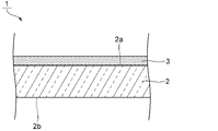
- FIG. 1 is a schematic cross-sectional view showing a transparent substrate with a film according to the first embodiment of the present invention.
- FIG. 2 is a schematic cross-sectional view showing a transparent substrate with a film according to a second embodiment of the present invention.
- FIG. 3 is a schematic cross-sectional view showing a transparent substrate with a film according to a third embodiment of the present invention.
- FIG. 4 is a schematic cross-sectional view showing a transparent substrate with a film according to a fourth embodiment of the present invention.
- FIG. 5 is a schematic cross-sectional view showing a top plate for a cooker according to an embodiment of the present invention.
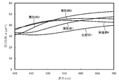
- FIG. 6 is a diagram showing the absorption coefficients of the light absorption films obtained in Examples 1 to 4 and Comparative Example 1 at wavelengths of 400 nm to 700 nm.
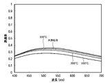
- FIG. 7 is a diagram showing a transmission spectrum of the transparent substrate with a film after the heat treatment of Example 3.
- FIG. 8 is a diagram showing the transmission spectrum of the transparent substrate with a film after the heat treatment of Comparative Example 1.
- FIG. 9 is a schematic cross-sectional view showing a transparent substrate with a film according to a fifth embodiment of the present invention.
- FIG. 10 is a schematic cross-sectional view showing a cover glass according to an embodiment of the present invention.
- FIG. 1 is a schematic cross-sectional view showing a transparent substrate with a film according to the first embodiment of the present invention.
- the transparent substrate 1 with a film includes a transparent substrate 2 and a light absorbing film 3.
- the transparent substrate 2 has a first main surface 2a and a second main surface 2b facing each other.
- a light absorption film 3 is provided on the first main surface 2a of the transparent substrate 2.
- the transparent substrate 2 has a substantially rectangular plate-like shape.
- the transparent substrate 2 may have a substantially disk-like shape, and the shape is not particularly limited.
- the transparent substrate 2 transmits light at a wavelength of 400 nm to 700 nm.
- the transparent substrate 2 may be colored and transparent, but is preferably colorless and transparent from the viewpoint of further enhancing the aesthetic appearance.
- transparent means that the light transmittance in the visible wavelength range at a wavelength of 400 nm to 700 nm is 80% or more.
- colorless means that the saturation of the transmitted light when irradiated with the D65 light source is 2 or less.
- the transparent substrate 2 is made of glass.
- the transparent substrate 2 may be made of another material such as ceramics as long as it is a transparent substrate.
- the glass constituting the transparent substrate 2 is preferably made of glass having a high glass transition temperature and low expansion, or crystallized glass having low expansion.
- Specific examples of the low-expansion crystallized glass include "N-0" manufactured by Nippon Electric Glass Co., Ltd.
- As the transparent substrate 2 borosilicate glass, non-alkali glass, aluminosilicate glass, or the like may be used. In this case, the heat resistance of the transparent substrate 2 can be further increased, and the coefficient of thermal expansion can be further reduced. Therefore, it can be suitably used for applications such as a top plate for a cooker in which heating and cooling are repeated.
- the thickness of the transparent substrate 2 is not particularly limited.
- the thickness of the transparent substrate 2 can be appropriately set according to the light transmittance and the like.
- the thickness of the transparent substrate 2 can be, for example, about 0.035 mm to 5 mm.
- the light absorption film 3 further contains O (oxygen).
- the method for forming the light absorption film 3 is not particularly limited, but for example, the film may be formed by a physical vapor deposition method (PVD method), a sputtering method, a pulse laser deposition method (PLD), a vapor deposition method, or the like. can.
- PVD method physical vapor deposition method
- PLD pulse laser deposition method
- vapor deposition method or the like. can.
- the light absorption film 3 can be formed into a film by using, for example, a mixed target of Ag, Al, and FeO. Further, the mixed target of Ag and FeO and the target of Al may be used separately. In addition, FeO may not be contained in each target.
- the substrate temperature is set to 15 ° C to 400 ° C
- the flow rate of the inert gas such as argon gas as the sputtering gas is set to 10 sccm to 1000 sccm
- the flow rate of oxygen gas is set to 0 sccm to 400 sccm.
- the electric power can be set to 1 kW to 60 kW.
- the transparent substrate 1 with a film of the present embodiment has the above-mentioned configuration, the display of various information can be clearly seen when the light source is turned on, and the display can be made excellent in aesthetics when the light source is turned off. .. In particular, the optical characteristics are unlikely to change even with heating, and excellent aesthetics can be stably maintained when the light source is turned off. This point can be explained as follows.
- the material constituting the inorganic pigment layer strongly absorbs the short wavelength side (purple or blue side; high energy of light) of visible light, and the long wavelength side (red side; light). It is a problem that it does not become achromatic black because it absorbs weakly (low energy).
- the light absorption on the short wavelength side of visible light is carried out by the light absorption by the band gap of iron oxide such as Fe 2 O 3 , and the light absorption on the long wavelength side is carried out by Ag. Since it can be carried by light absorption by free electrons, the top plate becomes achromatic black even when it is turned off, and it has excellent aesthetics. Further, by replacing a part or all of iron oxide with aluminum oxide, heat resistance can be improved while maintaining light absorption on the short wavelength side of visible light.
- the absorption coefficient due to the band gap of iron oxide or the like responsible for light absorption on the short wavelength side of visible light is proportional to the nth power of the inverse of the wavelength
- the absorption coefficient by free electrons of Ag responsible for light absorption on the long wavelength side is Since it is proportional to the square of the wavelength
- the absorption coefficient ⁇ ( ⁇ ) of the light absorption film 3 represented by the sum of these is generally independent of the wavelength and tends to be a constant value at any wavelength.
- the transparent substrate 1 with a film provided with the light absorption film 3 can uniformly absorb light particularly in almost the entire range of visible light. Moreover, since the heat resistance is enhanced, the optical characteristics are unlikely to change due to heating. Therefore, the transparent substrate 1 with a film can be achromatic black when the light source is turned off, and is stable and excellent in aesthetics. Therefore, the transparent substrate 1 with a film can be suitably used for applications such as a top plate for a cooker and a cover glass for a display.
- the content ratio (y / (y + z)) of Al to the total of Al and Fe is preferably 0.10 or more, more preferably 0.30 or more, and further preferably 0. It is 50 or more, particularly preferably 0.60 or more.
- the content ratio (y / (y + z)) may be 1.0 in terms of molar ratio.
- the Ag content ratio (x / (x + y + z)) to the total of Ag, Al, and Fe is preferably 0.05 or more, more preferably 0.12 or more, and preferably 0.12 or more in terms of molar ratio. It is 0.90 or less, more preferably 0.80 or less.
- the content ratio (x / (x + y + z)) is within the above range, the light absorption on the long wavelength side of visible light can be appropriately increased, and the light is absorbed more uniformly over almost the entire range of visible light. And even higher electrical insulation can be obtained.
- the content ratio (y / (x + y + z)) of Al to the total of Ag, Al, and Fe is preferably 0.04 or more, more preferably 0.27 or more, and preferably 0.27 or more in terms of molar ratio. It is 0.95 or less, more preferably 0.80 or less.
- the content ratio (y / (x + y + z)) is within the above range, it is possible to make it even more difficult for the optical characteristics to change due to heating.
- the Fe content ratio (z / (x + y + z)) to the total of Ag, Al, and Fe is preferably 0.08 or more, more preferably 0.18 or more, and preferably 0.18 or more in terms of molar ratio. It is 0.76 or less, more preferably 0.64 or less.
- the content ratio (z / (x + y + z)) is within the above range, the light absorption on the short wavelength side of visible light can be appropriately increased, and the light is absorbed more uniformly over almost the entire range of visible light. can do.
- the contents of Ag, Al, and Fe in the light absorption film 3 can be measured by energy dispersive X-ray analysis, wavelength dispersive X-ray analysis, inductively coupled plasma mass analysis, and the like.
- the present invention it is preferable that aluminum oxide and / or iron oxide form a matrix in the light absorption film 3, and Ag is dispersed in the matrix.
- the insulating property of the light absorption film 3 can be further improved.
- a part of Ag may be present as a matrix component. Therefore, in this case, it can be suitably used for a display having a touch panel function or a top plate for a cooker having a built-in display having a touch panel function.
- the average absorption coefficient of the light absorption film 3 having a wavelength of 400 nm to 700 nm is preferably 0.5 ⁇ m -1 or more, more preferably 10 ⁇ m -1 or more, preferably 80 ⁇ m -1 or less, and more preferably 70 ⁇ m -1 or less.
- the average absorption coefficient is not more than the above lower limit value, for example, when it is used for a top plate for a cooker, the structure inside the cooker can be more reliably concealed.
- the average absorption coefficient is not more than the above upper limit value, it is possible to make the display of various information more surely and clearly visible when the light source is turned on.
- the absorption coefficient of the light absorption film 3 is derived from the measurement of transmittance and reflectance by spectroscopic ellipsometry or a spectrophotometer, and in that case, the light absorption film is laminated on the transparent substrate 2. It shall be measured from the 3 side.
- the absorption coefficient at a wavelength of 436 nm when the absorption coefficient at a wavelength of 436 nm is ⁇ 1, the absorption coefficient at a wavelength of 546 nm is ⁇ 2, and the absorption coefficient at a wavelength of 700 nm is ⁇ 3, ⁇ 1 / ⁇ 2 is 0.8 or more and 2.0. It is preferable that ⁇ 3 / ⁇ 2 is 0.8 or more and 2.0 or less. Further, it is more preferable that ⁇ 1 / ⁇ 2 is 0.8 or more and 1.25 or less, and ⁇ 3 / ⁇ 2 is 0.8 or more and 1.25 or less. In this case, when the light source is turned off, the color can be made more achromatic black, and the aesthetics can be further improved.
- the absorption average deviation M represented by the following equation (1) is 0.30.
- the following is preferable.
- the color can be made more achromatic black, and the aesthetics can be further improved.
- the content of Ag in the light absorption film 3 is mol%, preferably 5% or more, more preferably 10% or more, still more preferably 12% or more, preferably 80% or less, more preferably 70. % Or less, more preferably 60% or less, and particularly preferably 55% or less. If the Ag content in the light absorption film 3 is smaller than the lower limit, the ⁇ 1 / ⁇ 2 may be too large, the ⁇ 3 / ⁇ 2 may be too small, and the absorption average deviation M may be large. It may be too much. On the other hand, if the content of Ag in the light absorption film 3 is larger than the above upper limit value, the sheet resistance may easily decrease. Further, the ⁇ 1 / ⁇ 2 may be too small, the ⁇ 3 / ⁇ 2 may be too large, and the absorption average deviation M may be too large.
- the thickness of the light absorption film 3 is not particularly limited, but is preferably 5 nm or more, more preferably 10 nm or more, still more preferably 15 nm or more, particularly preferably 20 nm or more, preferably 2 ⁇ m or less, more preferably 1 ⁇ m or less, still more preferably. It is 500 nm or less, particularly preferably 100 nm or less.
- the display of various information can be made more clearly visible when the light source is turned on, and the display is made more aesthetically pleasing when the light source is turned off. Can be done.
- the saturation C * T of the transmitted light of the transparent substrate 1 with a film is preferably 2 or less, more preferably 1 or less, still more preferably 0.8 or less, and particularly preferably 0.5 or less.
- the lower limit of the saturation C * T of the transmitted light of the transparent substrate 1 with a film is not particularly limited, but is, for example, 0.
- the saturation C * R of the reflected light of the transparent substrate 1 with a film is preferably 2 or less, more preferably 1 or less, still more preferably 0.7 or less, and particularly preferably 0.5 or less.
- the lower limit of the saturation C * R of the reflected light of the transparent substrate 1 with a film is not particularly limited, but is, for example, 0.
- the saturation C * is the saturation C * when irradiated with the D65 light source in the L * a * b * color system adopted in JIS Z 8781-4: 2013.
- the color can be made more achromatic black, and the aesthetics can be further improved.
- the absolute value of the difference in the brightness (L * ) of the reflected light between the display area A and the non-display area B is preferable. Is 5 or less, more preferably 3 or less, still more preferably 1 or less.
- the lower limit of the absolute value of the difference in the brightness (L * ) of the reflected light between the display area A and the non-display area B is, for example, 0.
- the absolute value of the difference in saturation (C * R ) of the reflected light between the display area A and the non-display area B is preferably 0.7 or less, more preferably 0.4 or less, still more preferably 0.3. It is as follows.
- the lower limit of the absolute value of the difference in saturation (C * R ) of the reflected light between the display area A and the non-display area B is, for example, 0.
- the sheet resistance of the light absorption film 3 is preferably 105 ⁇ (105 ⁇ / ⁇ ) or more, more preferably 10 6 ⁇ ( 106 ⁇ / ⁇ ) or more, and further preferably 10 7 ⁇ ( 107 ⁇ / ⁇ ). ) That's all.
- the light absorbing film 3 is insulating, when used as a cover glass of an image display device or a top plate of a cooker, even if a touch panel is attached, the finger required for the capacitive touch sensor is used. The change in capacitance due to contact is maintained, and the touch panel can function.
- the upper limit of the sheet resistance of the light absorption film 3 is, for example, 10 15 ⁇ (10 15 ⁇ / ⁇ ).
- sheet resistance can be measured by the method specified in ASTM D257 or JIS K 6271-6 (2008).
- FIG. 2 is a schematic cross-sectional view showing a transparent substrate with a film according to a second embodiment of the present invention. As shown in FIG. 2, in the transparent substrate 21 with a film, a dielectric multilayer film 6 is further provided on the light absorption film 3. Other points are the same as those of the first embodiment.
- the dielectric multilayer film 6 is a laminated film in which a low refractive index film 7 having a relatively low refractive index and a high refractive index film 8 having a relatively high refractive index are alternately laminated in this order.
- the number of laminated dielectric multilayer films 6 is five.
- the outermost layer is a low refractive index film 7 as in the present embodiment, the function as an antireflection film can be further enhanced.
- Examples of the material of the low refractive index film 7 include silicon oxide as in the present embodiment and aluminum oxide.
- Examples of the material of the high refractive index film 8 include niobium oxide, titanium oxide, zirconium oxide, hafnium oxide, tantalum oxide, silicon nitride, aluminum oxide, and aluminum nitride as in the present embodiment.
- FIG. 3 is a schematic cross-sectional view showing a transparent substrate with a film according to a third embodiment of the present invention.
- a dielectric multilayer film 16 including a light absorption film 3 is provided on the first main surface 2a of the transparent substrate 2.
- Other points are the same as those of the first embodiment.
- a low refractive index film 7 having a relatively low refractive index and a light absorbing film 3 as a high refractive index film having a relatively high refractive index are alternately laminated in this order.
- the number of laminated dielectric multilayer films 16 is five.
- the light absorption film 3 is the light absorption film 3 described in the first embodiment
- the low refractive index film 7 is the low refractive index film 7 described in the second embodiment.
- at least one layer of the light absorption film 3 having two layers may be the high refractive index film 8 described in the second embodiment.
- FIG. 4 is a schematic cross-sectional view showing a transparent substrate with a film according to a fourth embodiment of the present invention.
- the transparent substrate 41 with a film two layers of the light absorption film 3 are provided on the transparent substrate 2, and the space between the transparent substrate 2 and the light absorption film 3 and the two light absorption films 3 and 3 are provided.
- a dielectric multilayer film is further provided between them.
- Other points are the same as those of the second embodiment.
- FIG. 9 is a schematic cross-sectional view showing a transparent substrate with a film according to a fifth embodiment of the present invention.
- a dielectric multilayer film 66 including a light absorption film 3 is provided on the first main surface 2a of the transparent substrate 2.
- Other points are the same as those of the first embodiment.
- a high refractive index film 8 having a relatively high refractive index and a light absorbing film 3 as a low refractive index film having a relatively low refractive index are alternately laminated in this order.
- the outermost layer is provided with a low refractive index film 7 which is a silicon oxide film (SiO 2 film).
- SiO 2 film silicon oxide film
- the number of laminated dielectric multilayer films 66 is six.
- the light absorption film 3 is the light absorption film 3 described in the first embodiment
- the high refractive index film 8 is the high refractive index film 8 described in the second embodiment.
- One layer of the two light absorption films 3 may be the low refractive index film 7 described in the second embodiment.
- the dielectric multilayer film 6 may be provided on the light absorbing film 3 as in the second embodiment, or the light absorbing film 6 may be provided on the transparent substrate 2 as in the third and fifth embodiments.
- a dielectric multilayer film including the film 3 may be provided, or two layers of the light absorbing film 3 are provided on the transparent substrate 2 as in the fourth embodiment, and the transparent substrate 2 and the light absorbing film 3 are provided.
- a dielectric multilayer film may be further provided between the space and between the two light absorbing films 3 and 3. When such a dielectric multilayer film is provided, for example, an antireflection function can be further imparted. In this case, the contrast of the display can also be improved.
- the light absorption film 3 may be used as a high refractive index film as in the third embodiment, and the light absorption film 3 may be used as a low refractive index film as in the fifth embodiment. You may.
- the light absorption film 3 can be used as a low refractive index film or a high refractive index film by adjusting the magnitude of the refractive index according to the film forming conditions such as the target composition and the film forming pressure.
- the refractive index of the light absorption film 3 can be adjusted, for example, in the range of 1.2 or more and 2.0 or less.
- the total number of layers of the low refractive index film 7 and the high refractive index film 8 can be, for example, two or more and 40 or less.
- the thickness of the low refractive index film 7 can be, for example, 5 nm or more and 300 nm or less per layer.
- the thickness of the high refractive index film 8 can be, for example, 3 nm or more and 200 nm or less per layer. When the light absorption film 3 is used, the thickness may be the thickness described in the first embodiment.
- FIG. 5 is a schematic cross-sectional view showing a top plate for a cooker according to an embodiment of the present invention. As shown in FIG. 5, the cooker top plate 51 includes a transparent substrate 1 with a film.
- the second main surface 2b of the transparent substrate 2 constituting the transparent substrate 1 with a film is a cooking surface.
- the first main surface 2a of the transparent substrate 2 constituting the transparent substrate 1 with a film is the back surface.
- the cooking surface is the surface on which cooking utensils such as pots and frying pans are placed.
- the back surface is a surface facing a light source 52 such as an LED or a display or a heating device on the inner side of the cooker. Therefore, the cooking surface and the back surface are in a front-to-back relationship.
- the transparent substrate 2 is made of low-expansion crystallized glass.
- a light absorption film 3 is provided on the back surface (first main surface 2a) of the transparent substrate 2.
- a heat-resistant resin layer 53 is provided on the light absorption film 3.
- the heat-resistant resin layer 53 may be provided between the transparent substrate 2 and the light absorption film 3.
- the region in which the heat-resistant resin layer 53 is not provided is designated as the display region A in a plan view. Further, the region where the heat-resistant resin layer 53 is provided in a plan view is defined as a non-display region B.
- the heat-resistant resin layer 53 is a light-shielding layer. Therefore, by providing the heat-resistant resin layer 53, the concealing property of the internal structure of the cooker can be further reliably enhanced.
- the heat-resistant resin layer 53 can be made of a heat-resistant resin such as a silicone resin, a coloring pigment, or the like. The heat-resistant resin layer 53 may not be provided.
- a light source 52 such as a display or an LED is provided below the transparent substrate 1 with a film.
- the light source 52 is a member provided for displaying information in the display area A.
- the information to be displayed in the display area A is not particularly limited, and for example, information indicating the state of the cooker such as that the power is on or heating is being performed, time, and the like. Information is given.
- the light from the light source 52 passes through the light absorption film 3 and the transparent substrate 2 and is emitted to the outside. Further, the light from the light source 52 is shielded by the heat-resistant resin layer 53 in the non-display region B. Therefore, in the display area A, characters, numbers, symbols, and the like can be displayed by transmitting the light from the light source 52.
- the top plate 51 for a cooker includes a transparent substrate 1 with a film. Therefore, when the light source 52 is turned on, the display of various information can be clearly seen, and when the light source 52 is turned off, the display can be made excellent in aesthetics. Further, it is possible to make the boundary between the display area A and the non-display area B difficult to see while concealing the structure inside the cooker. A display having a touch panel function may be built in the cooker.
- FIG. 10 is a schematic cross-sectional view showing a cover glass according to an embodiment of the present invention.
- the cover glass 71 includes a transparent substrate 1 with a film.
- the cover glass 71 is, for example, a cover glass that is arranged and used in front of the display.
- the first main surface 2a of the transparent substrate 2 constituting the transparent substrate 1 with a film is the main surface arranged on the outside.
- the second main surface 2b of the transparent substrate 2 constituting the transparent substrate 1 with a film is the main surface on the display side. Therefore, in the cover glass 71, the light absorption film 3 is provided on the main surface (first main surface 2a) opposite to the side on which the display of the transparent substrate 2 is provided.
- the cover glass 71 is also provided with the transparent substrate 1 with a film, the optical characteristics are unlikely to change due to heating, and the aesthetics are excellent when the light source is turned off.
- the antireflection film may be formed by using the dielectric multilayer film as described in the second to fifth embodiments.
- Example 1 In Example 1, light is applied onto a glass substrate (manufactured by Nippon Electric Glass Co., Ltd., trade name “N-0”, thickness: 4 mm) which is a transparent substrate by a sputtering method using a mixed target of Ag, Al, and FeO. An absorbent film was formed.
- the Ag content in the mixed target was 60 mol%.
- the substrate temperature at this time was 300 ° C., and the oxygen partial pressure was 0.5 Pa.
- the Ag content in the light absorption film was 88 mol%.
- the Al content ratio (y / (y + z)) (Al / (Al + Fe)) to the total of Al and Fe was 0.14 in terms of molar ratio.
- the compositions of Ag, Al, and Fe were measured by inductively coupled plasma mass spectrometry.
- Examples 2 to 4 and Comparative Example 1 The same as in Example 1 except that the target composition was changed so that the Al content (y / (y + z)) with respect to the total of Al and Fe was changed as shown in Table 1 below in terms of molar ratio. A light absorbing film was formed.
- FIG. 6 is a diagram showing the absorption coefficients of the light absorption films obtained in Examples 1 to 4 and Comparative Example 1 at wavelengths of 400 nm to 700 nm. From FIG. 6, it can be seen that in the light absorption films obtained in Examples 1 to 4, the absorption coefficient is almost constant at a wavelength of 400 nm to 700 nm, similarly to the light absorption films obtained in Comparative Example 1. In the light absorption films obtained in Examples 1 to 4 and Comparative Example 1, when the absorption coefficient at a wavelength of 436 nm is ⁇ 1, the absorption coefficient at a wavelength of 546 nm is ⁇ 2, and the absorption coefficient at a wavelength of 700 nm is ⁇ 3.
- the saturation C * T of the transmitted light and the saturation C * R of the reflected light in the transparent substrate with a film obtained in Examples 1 to 4 and Comparative Example 1 were determined.
- the saturation C * conforms to JIS Z 8781-4: 2013, and the saturation C * T of the transmitted light uses a spectral transmittance meter (manufactured by Hitachi High-Tech Science Co., Ltd., product number "U-4100").
- the saturation C * R of the reflected light is the brightness (L * ) and chromaticity (a) when the D65 light source is irradiated from the side opposite to the film forming surface using a color difference meter (“CM2600d” manufactured by Konica Minolta).
- the portion of the transparent substrate with a film provided with the light absorption film is used as a display area, and a heat-resistant resin layer having a thickness of 15 ⁇ m is separately formed on the light-absorbing film, and the portion provided with the heat-resistant resin layer is used. It was set as a hidden area.
- the heat-resistant resin layer was prepared by mixing 34 parts by mass of a silicone resin, 29 parts by mass of a black pigment, and 37 parts by mass of a solvent to prepare a paste and applying it on a light absorbing film.
- the absolute value of the difference in the saturation C * R of the reflected light between the display area and the non-display area, and the difference in the brightness (L * ) of the reflected light was calculated.
- Example 3 The transparent substrates with a film obtained in Example 3 and Comparative Example 1 were heat-treated at temperatures of 100 ° C., 200 ° C., and 300 ° C. for 10 minutes, respectively.
- the transmittance difference from the unheat-treated product at wavelengths of 436 nm, 546 nm, and 700 nm was measured. The results are shown in Table 2 below.
- FIG. 7 is a diagram showing a transmission spectrum of the transparent substrate with a film after the heat treatment of Example 3.
- FIG. 8 is a diagram showing the transmission spectrum of the transparent substrate with a film after the heat treatment of Comparative Example 1.
- the transmission spectrum of the transparent substrate with a film which has not been heat-treated is also shown.
- Example 5 A dielectric multilayer film is prepared by a sputtering method on a transparent glass substrate (manufactured by Nippon Electric Glass Co., Ltd., trade name "T2X-1", thickness: 1.3 mm, refractive index: 1.52 (wavelength 550 nm)). did. Specifically, in the configuration shown in Table 3 below, the light absorption film of Example 3, the niobium oxide film (Nb 2 O 5 ) film, the light absorption film of Example 3, and the silicon oxide film are formed on a glass substrate. A dielectric multilayer film was produced so that (SiO 2 films) were alternately laminated in this order.
- the refractive index is a refractive index having a wavelength of 550 nm.
- the transmission spectrum and the reflection spectrum were measured from the film-forming surface side using a spectral transmittance meter (manufactured by Hitachi High-Tech Science Co., Ltd., product number "U-4100"). Specifically, the incident angle (AOI) was set to 0 °, 15 °, 30 °, and 45 °, and the measurement wavelength range was set to 380 nm to 780 nm. From the obtained transmittance spectrum and reflectance spectrum, the visual reflectance, the visual transmittance, the brightness (L * ) of the reflected light and the transmitted light, and the chromaticity (a * and b * ) when irradiated with the D65 light source. Asked. The results are shown in Table 4 below.
- Example 6 A dielectric multilayer film was prepared by sputtering on a transparent glass substrate (manufactured by Nippon Electric Glass Co., Ltd., trade name "T2X-1", thickness: 1.3 mm, refractive index: 1.52 (wavelength 550 nm)). .. Specifically, in the configuration shown in Table 5 below, a silicon nitride film (SiN film), a light absorption film of Example 3, a SiN film, a light absorption film of Example 3, a SiN film, and a glass substrate have the configuration shown in Table 5 below. A dielectric multilayer film was produced so that the SiO 2 films were alternately laminated in this order.
- the refractive index is a refractive index having a wavelength of 550 nm.
- the transmission spectrum and the reflection spectrum were measured from the film-forming surface side using a spectral transmittance meter (manufactured by Hitachi High-Tech Science Co., Ltd., product number "U-4100"). Specifically, the incident angle (AOI) was set to 0 °, 15 °, 30 °, and 45 °, and the measurement wavelength range was set to 380 nm to 780 nm. From the obtained transmittance spectrum and reflectance spectrum, the visual reflectance, the visual transmittance, the brightness (L * ) of the reflected light and the transmitted light, and the chromaticity (a * and b * ) when irradiated with the D65 light source. Asked. The results are shown in Table 6 below.
- Example 7 A dielectric multilayer film was produced by sputtering on a transparent glass substrate (manufactured by Nippon Electric Glass Co., Ltd., trade name "N-0", thickness: 4 mm, refractive index: 1.54 (wavelength 550 nm)). Specifically, in the configuration shown in Table 7 below, the Nb 2 O 5 film, the light absorption film of Example 3, the Nb 2 O 5 film, the light absorption film of Example 3, and the SiO are placed on the glass substrate 2. A dielectric multilayer film was prepared so that the two films were alternately laminated in this order.
- the refractive index is a refractive index having a wavelength of 550 nm.
- the transmission spectrum and the reflection spectrum are measured from the side opposite to the film forming surface using a spectral transmittance meter (manufactured by Hitachi High-Tech Science Co., Ltd., product number "U-4100"). did. Specifically, the incident angle (AOI) was set to 0 °, 15 °, 30 °, and 45 °, and the measurement wavelength range was set to 380 nm to 780 nm. From the obtained transmittance spectrum and reflectance spectrum, the visual reflectance, the visual transmittance, the brightness (L * ) of the reflected light and the transmitted light, and the chromaticity (a * and b * ) when irradiated with the D65 light source. Asked. The results are shown in Table 8 below.
- Example 8 A dielectric multilayer film was produced by sputtering on a transparent glass substrate (manufactured by Nippon Electric Glass Co., Ltd., trade name "N-0", thickness: 4 mm, refractive index: 1.54 (wavelength 550 nm)). Specifically, in the configuration shown in Table 9 below, the SiN film, the light absorption film of Example 3, the SiN film, the light absorption film of Example 3, and the SiN film are alternately laminated in this order on the glass substrate. As described above, a dielectric multilayer film was prepared.
- the refractive index is a refractive index having a wavelength of 550 nm.
- the transmission spectrum and the reflection spectrum are measured from the side opposite to the film forming surface using a spectral transmittance meter (manufactured by Hitachi High-Tech Science Co., Ltd., product number "U-4100"). did. Specifically, the incident angle (AOI) was set to 0 °, 15 °, 30 °, and 45 °, and the measurement wavelength range was set to 380 nm to 780 nm. From the obtained transmittance spectrum and reflectance spectrum, the visual reflectance, the visual transmittance, the brightness (L * ) of the reflected light and the transmitted light, and the chromaticity (a * and b * ) when irradiated with the D65 light source. Asked. The results are shown in Table 10 below.
- the transparent substrates with a film obtained in Examples 5 to 8 had small a * and b * , and the reflected color and the transmitted color were neutral. Further, it was confirmed that in the transparent substrates with a film obtained in Examples 5 to 8, a * and b * were hard to change, and there was almost no color shift in the incident angle range of 0 ° to 45 °.
Landscapes
- Chemical & Material Sciences (AREA)
- Engineering & Computer Science (AREA)
- Geochemistry & Mineralogy (AREA)
- Life Sciences & Earth Sciences (AREA)
- Chemical Kinetics & Catalysis (AREA)
- General Chemical & Material Sciences (AREA)
- Materials Engineering (AREA)
- Organic Chemistry (AREA)
- Ceramic Engineering (AREA)
- Combustion & Propulsion (AREA)
- Mechanical Engineering (AREA)
- General Engineering & Computer Science (AREA)
- Surface Treatment Of Glass (AREA)
- Laminated Bodies (AREA)
- Induction Heating Cooking Devices (AREA)
Priority Applications (3)
| Application Number | Priority Date | Filing Date | Title |
|---|---|---|---|
| JP2022569833A JP7828588B2 (ja) | 2020-12-16 | 2021-11-29 | 膜付き透明基板及び調理器用トッププレート |
| CN202180085268.8A CN116710413A (zh) | 2020-12-16 | 2021-11-29 | 带膜的透明基板和烹调器用顶板 |
| EP21906316.1A EP4265576A4 (en) | 2020-12-16 | 2021-11-29 | FILM-COVERED TRANSPARENT SUBSTRATE AND TOP PLATE FOR COOKING DEVICE |
Applications Claiming Priority (2)
| Application Number | Priority Date | Filing Date | Title |
|---|---|---|---|
| JP2020-208425 | 2020-12-16 | ||
| JP2020208425 | 2020-12-16 |
Publications (1)
| Publication Number | Publication Date |
|---|---|
| WO2022130953A1 true WO2022130953A1 (ja) | 2022-06-23 |
Family
ID=82059072
Family Applications (1)
| Application Number | Title | Priority Date | Filing Date |
|---|---|---|---|
| PCT/JP2021/043656 Ceased WO2022130953A1 (ja) | 2020-12-16 | 2021-11-29 | 膜付き透明基板及び調理器用トッププレート |
Country Status (4)
| Country | Link |
|---|---|
| EP (1) | EP4265576A4 (https=) |
| JP (1) | JP7828588B2 (https=) |
| CN (1) | CN116710413A (https=) |
| WO (1) | WO2022130953A1 (https=) |
Cited By (1)
| Publication number | Priority date | Publication date | Assignee | Title |
|---|---|---|---|---|
| WO2023120047A1 (ja) * | 2021-12-21 | 2023-06-29 | 日本電気硝子株式会社 | 膜付き透明基板、調理器用トッププレート、加熱調理器用窓ガラス、及びカバーガラス |
Citations (6)
| Publication number | Priority date | Publication date | Assignee | Title |
|---|---|---|---|---|
| JP2003261355A (ja) * | 2002-03-06 | 2003-09-16 | Central Glass Co Ltd | 電波透過性波長選択膜の製法 |
| JP2008540320A (ja) * | 2005-05-12 | 2008-11-20 | エージーシー フラット グラス ノース アメリカ,インコーポレイテッド | 低太陽熱利得係数、優れた化学及び機械的特性を有する低放射率コーティング及びその製造方法 |
| JP2014156358A (ja) * | 2011-06-10 | 2014-08-28 | Asahi Glass Co Ltd | 光学膜および合わせガラス |
| JP2014215018A (ja) | 2013-04-30 | 2014-11-17 | 日本電気硝子株式会社 | 調理器用トッププレート |
| JP2019123666A (ja) * | 2013-12-20 | 2019-07-25 | ユーロケラ ソシエテ オン ノーム コレクティフ | 誘導クッキングプレート及び製造方法 |
| JP2020510596A (ja) * | 2017-03-01 | 2020-04-09 | ガーディアン・グラス・エルエルシーGuardian Glass, Llc | 銀系赤外線(IR)反射層を保護するための銀ドープ保護層を有する(低放射率)low−Eコーティングを有するコーティングされた物品、及びその製造方法 |
Family Cites Families (6)
| Publication number | Priority date | Publication date | Assignee | Title |
|---|---|---|---|---|
| US20020037414A1 (en) * | 2000-07-18 | 2002-03-28 | Cunningham James A. | Low emissivity panel assembly |
| JP5016192B2 (ja) | 2004-02-18 | 2012-09-05 | 株式会社日本触媒 | 金属酸化物粒子およびその用途 |
| CN1922104A (zh) * | 2004-02-18 | 2007-02-28 | 株式会社日本触媒 | 金属氧化物颗粒及其应用 |
| FR2885995B1 (fr) | 2005-05-20 | 2007-07-06 | Eurokera | Plaque vitroceramique et son procede de fabrication |
| US10551740B2 (en) * | 2017-01-16 | 2020-02-04 | AGC Inc. | Transparent substrate with antireflective film having specified luminous transmittance and luminous reflectance |
| EP3992166B1 (en) * | 2019-07-01 | 2024-05-22 | Nippon Electric Glass Co., Ltd. | Film-covered transparent base plate and top plate for cooking device |
-
2021
- 2021-11-29 CN CN202180085268.8A patent/CN116710413A/zh active Pending
- 2021-11-29 EP EP21906316.1A patent/EP4265576A4/en active Pending
- 2021-11-29 WO PCT/JP2021/043656 patent/WO2022130953A1/ja not_active Ceased
- 2021-11-29 JP JP2022569833A patent/JP7828588B2/ja active Active
Patent Citations (6)
| Publication number | Priority date | Publication date | Assignee | Title |
|---|---|---|---|---|
| JP2003261355A (ja) * | 2002-03-06 | 2003-09-16 | Central Glass Co Ltd | 電波透過性波長選択膜の製法 |
| JP2008540320A (ja) * | 2005-05-12 | 2008-11-20 | エージーシー フラット グラス ノース アメリカ,インコーポレイテッド | 低太陽熱利得係数、優れた化学及び機械的特性を有する低放射率コーティング及びその製造方法 |
| JP2014156358A (ja) * | 2011-06-10 | 2014-08-28 | Asahi Glass Co Ltd | 光学膜および合わせガラス |
| JP2014215018A (ja) | 2013-04-30 | 2014-11-17 | 日本電気硝子株式会社 | 調理器用トッププレート |
| JP2019123666A (ja) * | 2013-12-20 | 2019-07-25 | ユーロケラ ソシエテ オン ノーム コレクティフ | 誘導クッキングプレート及び製造方法 |
| JP2020510596A (ja) * | 2017-03-01 | 2020-04-09 | ガーディアン・グラス・エルエルシーGuardian Glass, Llc | 銀系赤外線(IR)反射層を保護するための銀ドープ保護層を有する(低放射率)low−Eコーティングを有するコーティングされた物品、及びその製造方法 |
Non-Patent Citations (1)
| Title |
|---|
| See also references of EP4265576A4 |
Cited By (1)
| Publication number | Priority date | Publication date | Assignee | Title |
|---|---|---|---|---|
| WO2023120047A1 (ja) * | 2021-12-21 | 2023-06-29 | 日本電気硝子株式会社 | 膜付き透明基板、調理器用トッププレート、加熱調理器用窓ガラス、及びカバーガラス |
Also Published As
| Publication number | Publication date |
|---|---|
| CN116710413A (zh) | 2023-09-05 |
| JPWO2022130953A1 (https=) | 2022-06-23 |
| EP4265576A1 (en) | 2023-10-25 |
| JP7828588B2 (ja) | 2026-03-12 |
| EP4265576A4 (en) | 2024-11-27 |
Similar Documents
| Publication | Publication Date | Title |
|---|---|---|
| KR102640589B1 (ko) | 중성색 코팅을 갖는 커버 패널 | |
| JP2024150747A (ja) | 膜付き透明基板及び調理器用トッププレート | |
| CN114620944A (zh) | 颜色中性的防磨损层、具有防磨损层的基底及其制造方法 | |
| JP5182102B2 (ja) | 調理器用トッププレート | |
| JP7828588B2 (ja) | 膜付き透明基板及び調理器用トッププレート | |
| JP2011208820A (ja) | 調理器用トッププレート | |
| JP2022164641A (ja) | 板状のガラスまたはガラスセラミック要素、ならびにその製造方法およびその使用 | |
| JP2004211910A (ja) | 調理器用トッププレート | |
| WO2023120270A1 (ja) | 膜付き透明基板、調理器用トッププレート、加熱調理器用窓ガラス、及びカバーガラス | |
| JP7822567B2 (ja) | 膜付き透明基板、調理器用トッププレート、加熱調理器用窓ガラス、及びカバーガラス | |
| JP2025168284A (ja) | ガラスセラミック製の物品 | |
| JPH04209733A (ja) | 熱線遮へいガラス | |
| JP5700229B2 (ja) | 調理器用トッププレート | |
| JP2010190482A (ja) | 調理器用トッププレート |
Legal Events
| Date | Code | Title | Description |
|---|---|---|---|
| 121 | Ep: the epo has been informed by wipo that ep was designated in this application |
Ref document number: 21906316 Country of ref document: EP Kind code of ref document: A1 |
|
| ENP | Entry into the national phase |
Ref document number: 2022569833 Country of ref document: JP Kind code of ref document: A |
|
| WWE | Wipo information: entry into national phase |
Ref document number: 202180085268.8 Country of ref document: CN |
|
| NENP | Non-entry into the national phase |
Ref country code: DE |
|
| ENP | Entry into the national phase |
Ref document number: 2021906316 Country of ref document: EP Effective date: 20230717 |