WO2022123383A1 - 表示装置の作製方法 - Google Patents
表示装置の作製方法 Download PDFInfo
- Publication number
- WO2022123383A1 WO2022123383A1 PCT/IB2021/060953 IB2021060953W WO2022123383A1 WO 2022123383 A1 WO2022123383 A1 WO 2022123383A1 IB 2021060953 W IB2021060953 W IB 2021060953W WO 2022123383 A1 WO2022123383 A1 WO 2022123383A1
- Authority
- WO
- WIPO (PCT)
- Prior art keywords
- layer
- light emitting
- electrode
- oxide
- transistor
- Prior art date
- Legal status (The legal status is an assumption and is not a legal conclusion. Google has not performed a legal analysis and makes no representation as to the accuracy of the status listed.)
- Ceased
Links
Images
















Classifications
-
- H—ELECTRICITY
- H10—SEMICONDUCTOR DEVICES; ELECTRIC SOLID-STATE DEVICES NOT OTHERWISE PROVIDED FOR
- H10K—ORGANIC ELECTRIC SOLID-STATE DEVICES
- H10K59/00—Integrated devices, or assemblies of multiple devices, comprising at least one organic light-emitting element covered by group H10K50/00
- H10K59/80—Constructional details
- H10K59/805—Electrodes
- H10K59/8052—Cathodes
- H10K59/80522—Cathodes combined with auxiliary electrodes
-
- H—ELECTRICITY
- H05—ELECTRIC TECHNIQUES NOT OTHERWISE PROVIDED FOR
- H05B—ELECTRIC HEATING; ELECTRIC LIGHT SOURCES NOT OTHERWISE PROVIDED FOR; CIRCUIT ARRANGEMENTS FOR ELECTRIC LIGHT SOURCES, IN GENERAL
- H05B33/00—Electroluminescent light sources
- H05B33/02—Details
-
- H—ELECTRICITY
- H05—ELECTRIC TECHNIQUES NOT OTHERWISE PROVIDED FOR
- H05B—ELECTRIC HEATING; ELECTRIC LIGHT SOURCES NOT OTHERWISE PROVIDED FOR; CIRCUIT ARRANGEMENTS FOR ELECTRIC LIGHT SOURCES, IN GENERAL
- H05B33/00—Electroluminescent light sources
- H05B33/10—Apparatus or processes specially adapted to the manufacture of electroluminescent light sources
-
- H—ELECTRICITY
- H05—ELECTRIC TECHNIQUES NOT OTHERWISE PROVIDED FOR
- H05B—ELECTRIC HEATING; ELECTRIC LIGHT SOURCES NOT OTHERWISE PROVIDED FOR; CIRCUIT ARRANGEMENTS FOR ELECTRIC LIGHT SOURCES, IN GENERAL
- H05B33/00—Electroluminescent light sources
- H05B33/12—Light sources with substantially two-dimensional [2D] radiating surfaces
-
- H—ELECTRICITY
- H05—ELECTRIC TECHNIQUES NOT OTHERWISE PROVIDED FOR
- H05B—ELECTRIC HEATING; ELECTRIC LIGHT SOURCES NOT OTHERWISE PROVIDED FOR; CIRCUIT ARRANGEMENTS FOR ELECTRIC LIGHT SOURCES, IN GENERAL
- H05B33/00—Electroluminescent light sources
- H05B33/12—Light sources with substantially two-dimensional [2D] radiating surfaces
- H05B33/22—Light sources with substantially two-dimensional [2D] radiating surfaces characterised by the chemical or physical composition or the arrangement of auxiliary dielectric or reflective layers
-
- H—ELECTRICITY
- H05—ELECTRIC TECHNIQUES NOT OTHERWISE PROVIDED FOR
- H05B—ELECTRIC HEATING; ELECTRIC LIGHT SOURCES NOT OTHERWISE PROVIDED FOR; CIRCUIT ARRANGEMENTS FOR ELECTRIC LIGHT SOURCES, IN GENERAL
- H05B33/00—Electroluminescent light sources
- H05B33/12—Light sources with substantially two-dimensional [2D] radiating surfaces
- H05B33/26—Light sources with substantially two-dimensional [2D] radiating surfaces characterised by the composition or arrangement of the conductive material used as an electrode
- H05B33/28—Light sources with substantially two-dimensional [2D] radiating surfaces characterised by the composition or arrangement of the conductive material used as an electrode of translucent electrodes
-
- H—ELECTRICITY
- H10—SEMICONDUCTOR DEVICES; ELECTRIC SOLID-STATE DEVICES NOT OTHERWISE PROVIDED FOR
- H10D—INORGANIC ELECTRIC SEMICONDUCTOR DEVICES
- H10D30/00—Field-effect transistors [FET]
- H10D30/60—Insulated-gate field-effect transistors [IGFET]
- H10D30/67—Thin-film transistors [TFT]
- H10D30/674—Thin-film transistors [TFT] characterised by the active materials
- H10D30/6755—Oxide semiconductors, e.g. zinc oxide, copper aluminium oxide or cadmium stannate
-
- H—ELECTRICITY
- H10—SEMICONDUCTOR DEVICES; ELECTRIC SOLID-STATE DEVICES NOT OTHERWISE PROVIDED FOR
- H10K—ORGANIC ELECTRIC SOLID-STATE DEVICES
- H10K50/00—Organic light-emitting devices
- H10K50/10—OLEDs or polymer light-emitting diodes [PLED]
- H10K50/19—Tandem OLEDs
-
- H—ELECTRICITY
- H10—SEMICONDUCTOR DEVICES; ELECTRIC SOLID-STATE DEVICES NOT OTHERWISE PROVIDED FOR
- H10K—ORGANIC ELECTRIC SOLID-STATE DEVICES
- H10K59/00—Integrated devices, or assemblies of multiple devices, comprising at least one organic light-emitting element covered by group H10K50/00
- H10K59/10—OLED displays
- H10K59/12—Active-matrix OLED [AMOLED] displays
- H10K59/1201—Manufacture or treatment
-
- H—ELECTRICITY
- H10—SEMICONDUCTOR DEVICES; ELECTRIC SOLID-STATE DEVICES NOT OTHERWISE PROVIDED FOR
- H10K—ORGANIC ELECTRIC SOLID-STATE DEVICES
- H10K59/00—Integrated devices, or assemblies of multiple devices, comprising at least one organic light-emitting element covered by group H10K50/00
- H10K59/10—OLED displays
- H10K59/12—Active-matrix OLED [AMOLED] displays
- H10K59/121—Active-matrix OLED [AMOLED] displays characterised by the geometry or disposition of pixel elements
- H10K59/1213—Active-matrix OLED [AMOLED] displays characterised by the geometry or disposition of pixel elements the pixel elements being TFTs
-
- H—ELECTRICITY
- H10—SEMICONDUCTOR DEVICES; ELECTRIC SOLID-STATE DEVICES NOT OTHERWISE PROVIDED FOR
- H10K—ORGANIC ELECTRIC SOLID-STATE DEVICES
- H10K59/00—Integrated devices, or assemblies of multiple devices, comprising at least one organic light-emitting element covered by group H10K50/00
- H10K59/10—OLED displays
- H10K59/12—Active-matrix OLED [AMOLED] displays
- H10K59/124—Insulating layers formed between TFT elements and OLED elements
-
- H—ELECTRICITY
- H10—SEMICONDUCTOR DEVICES; ELECTRIC SOLID-STATE DEVICES NOT OTHERWISE PROVIDED FOR
- H10K—ORGANIC ELECTRIC SOLID-STATE DEVICES
- H10K59/00—Integrated devices, or assemblies of multiple devices, comprising at least one organic light-emitting element covered by group H10K50/00
- H10K59/80—Constructional details
- H10K59/805—Electrodes
- H10K59/8051—Anodes
-
- H—ELECTRICITY
- H10—SEMICONDUCTOR DEVICES; ELECTRIC SOLID-STATE DEVICES NOT OTHERWISE PROVIDED FOR
- H10K—ORGANIC ELECTRIC SOLID-STATE DEVICES
- H10K71/00—Manufacture or treatment specially adapted for the organic devices covered by this subclass
- H10K71/20—Changing the shape of the active layer in the devices, e.g. patterning
- H10K71/231—Changing the shape of the active layer in the devices, e.g. patterning by etching of existing layers
-
- H—ELECTRICITY
- H10—SEMICONDUCTOR DEVICES; ELECTRIC SOLID-STATE DEVICES NOT OTHERWISE PROVIDED FOR
- H10K—ORGANIC ELECTRIC SOLID-STATE DEVICES
- H10K71/00—Manufacture or treatment specially adapted for the organic devices covered by this subclass
- H10K71/60—Forming conductive regions or layers, e.g. electrodes
-
- H—ELECTRICITY
- H10—SEMICONDUCTOR DEVICES; ELECTRIC SOLID-STATE DEVICES NOT OTHERWISE PROVIDED FOR
- H10K—ORGANIC ELECTRIC SOLID-STATE DEVICES
- H10K71/00—Manufacture or treatment specially adapted for the organic devices covered by this subclass
- H10K71/621—Providing a shape to conductive layers, e.g. patterning or selective deposition
-
- H—ELECTRICITY
- H10—SEMICONDUCTOR DEVICES; ELECTRIC SOLID-STATE DEVICES NOT OTHERWISE PROVIDED FOR
- H10K—ORGANIC ELECTRIC SOLID-STATE DEVICES
- H10K59/00—Integrated devices, or assemblies of multiple devices, comprising at least one organic light-emitting element covered by group H10K50/00
- H10K59/30—Devices specially adapted for multicolour light emission
- H10K59/38—Devices specially adapted for multicolour light emission comprising colour filters or colour changing media [CCM]
Definitions
- One aspect of the present invention relates to a method for manufacturing a display device.
- one aspect of the present invention is not limited to the above technical fields.
- the technical field of one aspect of the invention disclosed in the present specification and the like relates to a product, a method, or a manufacturing method.
- one aspect of the invention relates to a process, machine, manufacture, or composition (composition of matter). Therefore, more specifically, the technical fields of one aspect of the present invention disclosed in the present specification include semiconductor devices, display devices, light emitting devices, power storage devices, storage devices, driving methods thereof, or manufacturing methods thereof. Can be given as an example.
- an active matrix type display device having a transistor for driving a display element in each pixel is known.
- an active matrix type liquid crystal display device also referred to as “liquid crystal display”
- an active matrix type light emitting display device using a light emitting element such as an organic EL element as a display element.
- organic display also known as "EL display”
- the organic EL display is a self-luminous display device, it has a wider viewing angle and higher responsiveness than a liquid crystal display. In addition, since the organic EL display does not require a backlight, it is easy to realize weight reduction, thinning, and low power consumption of the display device, and it has been actively studied in recent years.
- the organic EL element that functions as a pixel has a structure in which an anode and a cathode are overlapped with each other via a light emitting layer. Further, in an organic EL display, a partition wall is provided between adjacent pixels in order to prevent electrical interference between adjacent light emitting layers (Patent Document 1).
- Patent Document 2 when an organic EL layer such as a light emitting layer is formed of a small molecule material, a method is known in which a vacuum vapor deposition method using a metal mask is used (Patent Document 2).
- the partition wall (also referred to as "bank” or “bank”) provided between the pixels has effects such as improvement of display quality of the display device and reduction of power consumption.
- a certain amount of partition walls are required to obtain a sufficient effect, it is difficult to reduce the occupied area of the partition walls, and it is difficult to improve the pixel aperture ratio, increase the definition, and reduce the size. rice field.
- the metal mask is inferior in dimensional accuracy to the resist mask, it is difficult to improve the pixel aperture ratio and improve the definition in the formation of the light emitting layer using the metal mask. Further, the metal mask has a problem that it is easily deformed by the influence of heat generated by the vapor deposition source.
- One of the problems of one aspect of the present invention is to provide a display device or a semiconductor device having good display quality. Another issue is to provide a highly reliable display device, semiconductor device, or the like. Another issue is to provide a display device or a semiconductor device having low power consumption. Another issue is to provide a lightweight display device, a semiconductor device, or the like. Another issue is to provide a display device or a semiconductor device with high productivity. Alternatively, one of the issues is to provide a new display device, a semiconductor device, or the like.
- One aspect of the present invention is a step of forming an anode on an insulating layer, a step of forming an EL layer on the anode, a step of forming a cathode on the EL layer, an anode, an EL layer, and a cathode.
- a step of selectively removing a part of each to form a plurality of light emitting elements and a step of forming a conductive layer covering the plurality of light emitting elements are included, and the cathode of each of the plurality of light emitting elements is a conductive layer.
- This is a method for manufacturing a display device that is electrically connected and has a light-transmitting conductive layer.
- Another aspect of the present invention is a step of forming an anode on an insulating layer, a step of forming an EL layer on the anode, a step of forming a cathode on the EL layer, an anode, an EL layer, and the like.
- the plurality of light emitting elements including a step of selectively removing a part of each of the cathode and the cathode to form a plurality of light emitting elements and a step of forming a conductive layer on the plurality of light emitting elements.
- Another aspect of the present invention includes, in (1) or (2), a step of forming a plurality of transistors on a substrate and a step of forming an insulating layer on the plurality of transistors, and the insulating layer includes a step of forming an insulating layer on the plurality of transistors.
- the transistor preferably contains an oxide semiconductor in the semiconductor layer on which the channel is formed.
- the oxide semiconductor preferably contains at least one of indium and zinc.
- a display device or a semiconductor device having good display quality it is possible to provide a display device or a semiconductor device having good display quality.
- a highly reliable display device, semiconductor device, or the like can be provided.
- a display device or a semiconductor device having low power consumption it is possible to provide a lightweight display device, a semiconductor device, or the like.
- a display device or a semiconductor device having high productivity it is possible to provide a new display device, semiconductor device, or the like.
- 1A to 1C are views for explaining a configuration example of a display device.
- 2A to 2C are diagrams illustrating an example of a method for manufacturing the first element substrate.
- 3A and 3B are diagrams illustrating an example of a method for manufacturing the first element substrate.
- 4A and 4B are diagrams illustrating an example of a method for manufacturing the first element substrate.
- 5A and 5B are diagrams illustrating an example of a method for manufacturing the first element substrate.
- 6A and 6B are diagrams illustrating an example of a method for manufacturing the first element substrate.
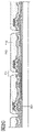
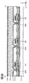
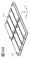
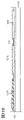
- 7A1, FIG. 7A2, and FIG. 7B are diagrams illustrating an example of a method for manufacturing the first element substrate.
- 8A and 8B are diagrams illustrating an example of a method for manufacturing the first element substrate.
- FIG. 9A and 9B are views for explaining a modification of the first element substrate.
- FIG. 10 is a diagram illustrating a modified example of the first element substrate.
- 11A to 11C are diagrams illustrating an example of a method for manufacturing the second element substrate.
- FIG. 12 is a diagram illustrating an example of a method for manufacturing a display device.
- FIG. 13 is a diagram illustrating a modified example of the display device.
- FIG. 14A is a diagram illustrating the classification of crystal structures.
- FIG. 14B is a diagram illustrating an XRD spectrum of a CAAC-IGZO film.
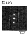
- FIG. 14C is a diagram illustrating a micro electron beam diffraction pattern of the CAAC-IGZO film.
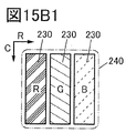
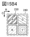
- FIGS. 15A and 15B1 to 15B5 are diagrams illustrating a configuration example of a display device.
- FIG. 16 is a diagram illustrating a configuration example of a pixel circuit.
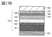
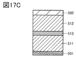
- 17A to 17C are views for explaining a configuration example of the light emitting element.
- 18A to 18F are views showing an example of an electronic device.
- the semiconductor device is a device utilizing semiconductor characteristics, and refers to a circuit including a semiconductor element (transistor, diode, photodiode, etc.), a device having the same circuit, and the like. It also refers to all devices that can function by utilizing semiconductor characteristics.
- a semiconductor element transistor, diode, photodiode, etc.
- the storage device, the display device, the light emitting device, the lighting device, the electronic device, and the like are themselves semiconductor devices, and may have a semiconductor device.
- an element for example, a switch, a transistor, a capacitive element, an inductor, a resistance element, a diode, a display
- One or more devices, light emitting devices, loads, etc. can be connected between X and Y.
- the switch is controlled in an on state and an off state. That is, the switch is in a conducting state (on state) or a non-conducting state (off state), and has a function of controlling whether or not a current flows.
- a circuit that enables functional connection between X and Y for example, a logic circuit (inverter, NAND circuit, NOR circuit, etc.), signal conversion) Circuits (digital-analog conversion circuit, analog-to-digital conversion circuit, gamma correction circuit, etc.), potential level conversion circuit (power supply circuit (boost circuit, step-down circuit, etc.), level shifter circuit that changes the signal potential level, etc.), voltage source, current source , Switching circuit, amplifier circuit (circuit that can increase signal amplitude or current amount, operational amplifier, differential amplifier circuit, source follower circuit, buffer circuit, etc.), signal generation circuit, storage circuit, control circuit, etc.), X and Y It is possible to connect one or more to and from. As an example, even if another circuit is sandwiched between X and Y, if the signal output from X is transmitted to Y, it is assumed that X and Y are functionally connected. do.
- X and Y are electrically connected, it means that X and Y are electrically connected (that is, another element between X and Y). Or when they are connected with another circuit in between) and when X and Y are directly connected (that is, they are connected without sandwiching another element or another circuit between X and Y). If there is) and.
- X and Y, the source (or the first terminal, etc.) and the drain (or the second terminal, etc.) of the transistor are electrically connected to each other, and the X, the source (or the second terminal, etc.) of the transistor are connected to each other. (1 terminal, etc.), the drain of the transistor (or the 2nd terminal, etc.), and Y are electrically connected in this order.
- the source of the transistor (or the first terminal, etc.) is electrically connected to X
- the drain of the transistor (or the second terminal, etc.) is electrically connected to Y
- the X, the source of the transistor (such as the second terminal).
- first terminal, etc.), the drain of the transistor (or the second terminal, etc.), and Y are electrically connected in this order.
- X is electrically connected to Y via the source (or first terminal, etc.) and drain (or second terminal, etc.) of the transistor, and X, the source (or first terminal, etc.) of the transistor.
- the terminals, etc.), the drain of the transistor (or the second terminal, etc.), and Y are provided in this connection order.
- the source (or first terminal, etc.) and drain (or second terminal, etc.) of the transistor can be separated. Separately, the technical scope can be determined. It should be noted that these expression methods are examples, and are not limited to these expression methods.
- X and Y are objects (for example, devices, elements, circuits, wirings, electrodes, terminals, conductive films, layers, etc.).
- the circuit diagram shows that the independent components are electrically connected to each other, the case where one component has the functions of a plurality of components together.
- one component has the functions of a plurality of components together.
- one conductive film has both the function of the wiring and the function of the components of the function of the electrode. Therefore, the electrical connection in the present specification also includes the case where one conductive film has the functions of a plurality of components in combination.
- the “resistance element” for example, a circuit element having a resistance value higher than 0 ⁇ , wiring and the like can be used. Therefore, in the present specification and the like, the “resistance element” includes wiring having a resistance value, a transistor in which a current flows between a source and a drain, a diode, a coil, and the like. Therefore, the term “resistance element” can be paraphrased into terms such as “resistance”, “load”, and “region having resistance value”, and conversely, the terms “resistance”, “load”, and “region having resistance value” are used. , Can be paraphrased into terms such as “resistance element”.
- the resistance value can be, for example, preferably 1 m ⁇ or more and 10 ⁇ or less, more preferably 5 m ⁇ or more and 5 ⁇ or less, and further preferably 10 m ⁇ or more and 1 ⁇ or less. Further, for example, it may be 1 ⁇ or more and 1 ⁇ 10 9 ⁇ or less.
- the resistance value may be determined by the length of the wiring.
- a conductor having a resistivity different from that of the conductor used as wiring may be used as the resistance element.
- the resistance value may be determined by doping the semiconductor with impurities.
- the “capacitance element” means, for example, a circuit element having a capacitance value higher than 0F, a wiring region having a capacitance value higher than 0F, a parasitic capacitance, and a transistor. Indicates the gate capacitance of. Therefore, in the present specification and the like, the “capacitive element” is not only a circuit element containing a pair of electrodes and a dielectric contained between the electrodes, but also a parasitic element generated between the wirings. It shall include the capacitance, the gate capacitance generated between the gate and one of the source or drain of the transistor, and the like.
- capacitor element means “capacitive element”, “parasitic capacitance”, and “capacity”. It can be paraphrased into terms such as “gate capacitance”.
- the term “pair of electrodes” of “capacity” can be paraphrased as "a pair of conductors", “a pair of conductive regions", “a pair of regions” and the like.
- the value of the capacitance can be, for example, 0.05 fF or more and 10 pF or less. Further, for example, it may be 1 pF or more and 10 ⁇ F or less.
- the transistor has three terminals called a gate, a source, and a drain.
- the gate is a control terminal that controls the conduction state of the transistor.
- the two terminals that act as sources or drains are the input and output terminals of the transistor.
- One of the two input / output terminals becomes a source and the other becomes a drain depending on the potential applied to the conductive type (n-channel type, p-channel type) of the transistor and the three terminals of the transistor. Therefore, in the present specification and the like, the terms source and drain can be paraphrased.
- the transistor when explaining the connection relationship of transistors, "one of the source or drain” (or the first electrode or the first terminal), “the other of the source or drain” (or the second electrode, or the second electrode, or The notation (second terminal) is used.
- it may have a back gate in addition to the above-mentioned three terminals.
- one of the gate or the back gate of the transistor may be referred to as a first gate
- the other of the gate or the back gate of the transistor may be referred to as a second gate.
- the terms “gate” and “backgate” may be interchangeable.
- the respective gates When the transistor has three or more gates, the respective gates may be referred to as a first gate, a second gate, a third gate, and the like in the present specification and the like.
- the "node” can be paraphrased as a terminal, a wiring, an electrode, a conductive layer, a conductor, an impurity region, etc., depending on the circuit configuration, device structure, and the like.
- terminals, wiring, etc. can be paraphrased as "nodes”.
- ground potential ground potential
- the potentials are relative, and when the reference potential changes, the potential given to the wiring, the potential applied to the circuit, the potential output from the circuit, and the like also change.
- high level potential also referred to as” high level potential ",” H potential “, or” H
- low level potential low level potential
- L low level potential
- the "current” is a charge transfer phenomenon (electrical conduction).
- the description “electrical conduction of a positively charged body is occurring” means “electrical conduction of a negatively charged body in the opposite direction”. Is happening. " Therefore, in the present specification and the like, “current” refers to a charge transfer phenomenon (electrical conduction) associated with carrier transfer, unless otherwise specified.
- the carrier here include electrons, holes, anions, cations, complex ions, and the like, and the carriers differ depending on the system in which the current flows (for example, semiconductor, metal, electrolytic solution, vacuum, etc.).
- the "current direction” in the wiring or the like is the direction in which the positive carrier moves, and is described as a positive current amount.
- the direction in which the negative carrier moves is opposite to the direction of the current, and is expressed by the amount of negative current. Therefore, in the present specification and the like, if there is no disclaimer regarding the positive or negative current (or the direction of the current), the description such as “current flows from element A to element B” is described as “current flows from element B to element A”. Can be rephrased as. Further, the description such as “a current is input to the element A” can be rephrased as "a current is output from the element A” or the like.
- the ordinal numbers “first”, “second”, and “third” are added to avoid confusion of the constituent elements. Therefore, the number of components is not limited. Moreover, the order of the components is not limited. For example, the component referred to in “first” in one of the embodiments of the present specification and the like is assumed to be the component referred to in “second” in another embodiment or in the scope of claims. It is possible. Further, for example, the component referred to in “first” in one of the embodiments of the present specification and the like may be omitted in other embodiments, claims, and the like.
- the terms indicating the arrangement such as “above”, “below”, “above”, or “below” explain the positional relationship between the components with reference to the drawings. In order to do so, it may be used for convenience. Further, the positional relationship between the constituent elements changes appropriately depending on the direction in which each configuration is depicted. Therefore, it is not limited to the words and phrases explained in the specification and the like, and can be appropriately paraphrased according to the situation. For example, in the expression of "insulator located on the upper surface of the conductor”, it can be paraphrased as "insulator located on the lower surface of the conductor” by rotating the direction of the drawing shown by 180 degrees.
- the terms “upper” and “lower” do not limit the positional relationship of the components to be directly above or directly below and to be in direct contact with each other.
- the electrode B does not have to be formed in direct contact with the insulating layer A, and another configuration is formed between the insulating layer A and the electrode B. Do not exclude those that contain elements.
- membrane and layer can be interchanged with each other depending on the situation.
- the term “conductive layer” may be changed to the term “conductive film”.
- the term “insulating film” may be changed to the term “insulating layer”.
- the term “conductive layer” or “conductive film” may be changed to the term “conductor”.
- the terms “insulating layer” and “insulating film” may be changed to the term “insulator”.
- Electrode may be used as part of a “wiring” and vice versa.
- the term “electrode” or “wiring” also includes the case where a plurality of “electrodes” or “wiring” are integrally formed.
- a “terminal” may be used as part of a “wiring” or “electrode” and vice versa.
- the term “terminal” includes a case where a plurality of "electrodes", “wiring”, “terminals” and the like are integrally formed.
- the "electrode” can be part of the “wiring” or “terminal”, and for example, the “terminal” can be part of the “wiring” or “electrode”.
- terms such as “electrode”, “wiring”, and “terminal” may be replaced with terms such as "area” in some cases.
- wiring can be interchanged with each other in some cases or depending on the situation.
- the term “wiring” may be changed to the term “signal line”.
- the term “wiring” may be changed to a term such as “power line”.
- the reverse is also true, and terms such as “signal line” and “power line” may be changed to the term “wiring”.
- a term such as “power line” may be changeable to a term such as “signal line”.
- terms such as “signal line” may be changed to terms such as “power line”.
- the term “potential” applied to the wiring may be changed to a term such as “signal” in some cases or depending on the situation. And vice versa, terms such as “signal” may be changeable to the term “potential”.
- the semiconductor impurities refer to, for example, other than the main components constituting the semiconductor layer.
- an element having a concentration of less than 0.1 atomic% is an impurity.
- the inclusion of impurities may result in, for example, an increase in the defect level density of the semiconductor, a decrease in carrier mobility, a decrease in crystallinity, and the like.
- the impurities that change the characteristics of the semiconductor include, for example, group 1 element, group 2 element, group 13 element, group 14 element, group 15 element, and other than the main component.
- transition metals and the like and in particular, hydrogen (also contained in water), lithium, sodium, silicon, boron, phosphorus, carbon, nitrogen and the like.
- the impurities that change the characteristics of the semiconductor include, for example, Group 1 elements excluding oxygen and hydrogen, Group 2 elements, Group 13 elements, Group 15 elements, and the like. There is.
- the switch means a switch that is in a conductive state (on state) or a non-conducting state (off state) and has a function of controlling whether or not a current flows.
- the switch means a switch having a function of selecting and switching a path through which a current flows.
- an electric switch, a mechanical switch, or the like can be used. That is, the switch is not limited to a specific switch as long as it can control the current.
- Examples of electrical switches include transistors (for example, bipolar transistors, MOS transistors, etc.), diodes (for example, PN diodes, PIN diodes, shotkey diodes, MIM (Metal Insulator Metal) diodes, and MIS (Metal Insulator Semiconductor) diodes. , Diode-connected transistors, etc.), or logic circuits that combine these.
- transistors for example, bipolar transistors, MOS transistors, etc.
- diodes for example, PN diodes, PIN diodes, shotkey diodes, MIM (Metal Insulator Metal) diodes, and MIS (Metal Insulator Semiconductor) diodes. , Diode-connected transistors, etc.
- the "conduction state" of the transistor means a state in which the source electrode and the drain electrode of the transistor can be regarded as being electrically short-circuited.
- non-conducting state means a state in which the source electrode and the drain electrode of the transistor can be
- a mechanical switch there is a switch using MEMS (Micro Electro Mechanical Systems) technology.
- the switch has an electrode that can be moved mechanically, and by moving the electrode, conduction and non-conduction are controlled and operated.
- parallel means a state in which two straight lines are arranged at an angle of ⁇ 10 ° or more and 10 ° or less. Therefore, the case of ⁇ 5 ° or more and 5 ° or less is also included.
- substantially parallel or approximately parallel means a state in which two straight lines are arranged at an angle of -30 ° or more and 30 ° or less.
- vertical means a state in which two straight lines are arranged at an angle of 80 ° or more and 100 ° or less. Therefore, the case of 85 ° or more and 95 ° or less is also included.
- substantially vertical or “approximately vertical” means a state in which two straight lines are arranged at an angle of 60 ° or more and 120 ° or less.
- a metal oxide is a metal oxide in a broad sense. Metal oxides are classified into oxide insulators, oxide conductors (including transparent oxide conductors), oxide semiconductors (also referred to as Oxide Semiconductor or simply OS) and the like. For example, when a metal oxide is used in the semiconductor layer on which the channel of the transistor is formed, the metal oxide may be referred to as an oxide semiconductor. That is, when a metal oxide is used as the semiconductor layer in which a channel is formed of a transistor having at least one of an amplification action, a rectifying action, and a switching action, the metal oxide is referred to as a metal oxide semiconductor (metal). It can be called an oxide semiconductor). Further, in the present specification and the like, a transistor containing a metal oxide or an oxide semiconductor in the semiconductor layer on which a channel is formed can be paraphrased as an “OS transistor”.
- the configuration shown in each embodiment can be appropriately combined with the configuration shown in other embodiments to form one aspect of the present invention. Further, when a plurality of configuration examples are shown in one embodiment, the configuration examples can be appropriately combined with each other.
- the size, layer thickness, or area may be exaggerated for clarity. Therefore, it is not necessarily limited to its size or aspect ratio.
- the drawings schematically show ideal examples, and are not limited to the shapes or values shown in the drawings. For example, it is possible to include variations in the signal, voltage, or current due to noise, or variations in the signal, voltage, or current due to timing deviation.
- identification characters such as [m, n] ”are added.
- one of the plurality of colored layers 131 may be described as the colored layer 131R, and the other one may be described as the colored layer 131G.
- a device manufactured by using a metal mask or an FMM may be referred to as a device having an MM (metal mask) structure.
- a device manufactured without using a metal mask or FMM may be referred to as a device having an MML (metal maskless) structure.
- FIG. 1A is a schematic perspective view of the display device 100.
- the display device 100 has a configuration in which the substrate 111 and the substrate 121 are bonded together.
- the display device 100 has a display area 235, a peripheral circuit area 232, a peripheral circuit area 233, and the like.
- FIG. 1 shows an example in which the FPC 124 is mounted on the display device 100. Therefore, the configuration shown in FIG. 1A can also be said to be a display module having a display device 100 and an FPC 124.
- the peripheral circuit area 232 and the peripheral circuit area 233 include a circuit for supplying a signal to the display area 235.
- the generic name of the circuits included in the peripheral circuit area 232 and the peripheral circuit area 233 may be referred to as "peripheral drive circuit".
- Examples of the circuit included in the peripheral drive circuit include a scan line drive circuit and a signal line drive circuit.
- a part or all of the peripheral drive circuit may be mounted by an IC (integrated circuit).
- an IC including a part or all of the peripheral drive circuit may be provided on the substrate 111 by a COG (Chip On Glass) method, a COF (Chip on Film) method, or the like. Further, the IC may be mounted on the FPC 124 by the COF method or the like.
- the signals and power supplied to the display area 235, the peripheral circuit area 232, and the peripheral circuit area 233 are input from the outside via the FPC 124.
- FIG. 1A an enlarged view of a part of the display area 235 is added.
- a plurality of pixels 240 are arranged in a matrix in the display area 235.
- the pixel 240 has a pixel 230R, a pixel 230G, and a pixel 230B.
- pixel 230 when the matter common to the pixel 230R, the pixel 230G, and the pixel 230B is explained, or when it is not necessary to distinguish between the three, it may be simply referred to as "pixel 230".
- FIG. 1B is a cross-sectional view of a portion shown by a dotted chain line of A1-A2 in FIG. 1A.
- FIG. 1B shows a cross section of a part of the display area 235, a part of the peripheral circuit area 233, and a part of the area including the FPC 124.
- Each of the pixel 230R, the pixel 230G, and the pixel 230B has a light emitting element 170 as a display element.
- the light emitting element 170 has an electrode 171 that functions as an anode, an EL layer 172, and an electrode 173 that functions as a cathode.
- each of the pixel 230R, the pixel 230G, and the pixel 230B has a transistor 251 for driving a display element.
- the peripheral circuit area 232 and the peripheral circuit area 233 have a plurality of transistors.
- the transistor 252 is shown as an example of the transistor included in the peripheral circuit region 233.
- the display device 100 has a transistor 251 and a transistor 252, a light emitting element 170, a colored layer 131 (colored layer 131R, a colored layer 131G, and a colored layer 131B), a light-shielding layer 132, and the like between the substrate 111 and the substrate 121.
- the substrate 111 and the substrate 121 are adhered to each other via the adhesive layer 142.
- various curable adhesives such as a photocurable adhesive such as an ultraviolet curable type, a reaction curable adhesive, a thermosetting adhesive, and an anaerobic adhesive can be used.
- these adhesives include epoxy resin, acrylic resin, silicone resin, phenol resin, polyimide resin, imide resin, PVC (polyvinyl chloride) resin, PVB (polyvinyl butyral) resin, EVA (ethylene vinyl acetate) resin and the like.
- a material having low moisture permeability such as an epoxy resin is preferable.
- a two-component mixed type resin may be used.
- an adhesive sheet or the like may be used.
- the substrate 121 is provided with an insulating layer 122, a colored layer 131, a light-shielding layer 132, an insulating layer 133, and the like.
- the insulating layer 133 may have a function as a flattening layer.
- the "flattening layer” refers to a layer having a surface with reduced unevenness on the surface to be formed.
- FIG. 1C shows an enlarged view of the transistor 252.
- the transistor 251 can also have the same structure as the transistor 252.
- the transistor 252 has an electrode 221, a semiconductor layer 231 and an electrode 224a, an electrode 224b, and an electrode 226.
- the electrode 221 is provided on the insulating layer 113, and the insulating layer 211 is provided so as to cover the electrode 221.
- a semiconductor layer 231 is provided on the insulating layer 211.
- An electrode 224a and an electrode 224b are provided on the insulating layer 211, the electrode 224a has a region in contact with a part of the semiconductor layer 231 and the electrode 224b has a region in contact with another part of the semiconductor layer 231.
- One of the electrode 224a or the electrode 224b can function as a source electrode.
- the other of the electrode 224a or the electrode 224b can function as a drain electrode.
- an insulating layer 210 is provided so as to cover the electrode 224a, the electrode 224b, and the semiconductor layer 231.
- An electrode 226 is provided on the insulating layer 210. The electrode 226 has a region overlapping the semiconductor layer 231.
- An insulating layer 213 is provided so as to cover the electrode 226.
- FIG. 1B illustrates a bottom gate type transistor as the transistor 251 and the transistor 252.
- the transistor 251 is a transistor (also referred to as a drive transistor) that controls the current flowing through the light emitting element 170.
- an insulating layer 114 is provided on the insulating layer 213.
- the insulating layer 114 has a function as a flattening layer.
- the transistor 251 and the transistor 252 are covered with an insulating layer 213 and an insulating layer 114.
- the number of insulating layers covering the transistor is not limited, and may be a single layer or two or more layers.
- the insulating layer can function as a barrier membrane.
- the electrode 171 is provided on the insulating layer 114.
- the electrode 171 is an opening provided in the insulating layer 114 and is electrically connected to either the source or the drain of the transistor 251.
- the EL layer 172 is provided on the electrode 171 and the electrode 173 is provided on the EL layer 172.
- the electrode 173 has a region that overlaps with the electrode 171 via the EL layer 172.
- the light emitting element 170 is covered with an insulating layer 115 and an insulating layer 116.
- the insulating layer 116 has a function as a flattening layer.
- a conductive layer 118 is provided on the insulating layer 116.
- the conductive layer 118 is electrically connected to the insulating layer 115 and the electrode 173 via an electrode 117 provided so as to be embedded in the insulating layer 116.
- the conductive layer 118 is electrically connected to the plurality of electrodes 173 and functions as a common electrode.
- a wiring 125, an electrode 228, and an electrode 229 are provided.
- the wiring 125 and the electrode 228 are provided on the insulating layer 211.
- the electrode 229 is electrically connected to the electrode 228 at an opening provided in the insulating layer 210 that overlaps with the electrode 228.
- the wiring 125 and the electrode 228 can be formed simultaneously in the same process as the electrodes 224a and 224b.
- the electrode 229 can be formed at the same time as the electrode 226 in the same process.
- the FPC 124 is electrically connected to the electrode 229 via the connection layer 138.
- the electrode 229 is electrically connected to the peripheral drive circuit.
- connection layer 138 an anisotropic conductive film (ACF: Anisotropic Conducive Film), an anisotropic conductive paste (ACP: Anisotropic Connective Paste), or the like can be used.
- ACF Anisotropic Conducive Film
- ACP Anisotropic Connective Paste
- the light emitting element 170 is, for example, a top emission type light emitting element.
- the light emitting element 170 has a laminated structure in which an electrode 171 functioning as an anode, an EL layer 172, and an electrode 173 functioning as a cathode are laminated in this order from the insulating layer 114 side.
- the electrode 171 When the light emitting element 170 is a top emission type light emitting element, the electrode 171 has a function of reflecting visible light, and the electrode 173 has a function of transmitting visible light.
- the conductive layer 118 also has a function of transmitting visible light.
- the EL layer 172 has at least a light emitting layer. Further, as a layer other than the light emitting layer, the EL layer 172 includes a substance having a high hole injecting property, a substance having a high hole transporting property, a hole blocking material, a substance having a high electron injecting property, a substance having a high electron transporting property, and an electron. It may have a layer containing a block material, a bipolar substance (a substance having high electron transport property and a hole transport property), and the like.
- the emission color of the light emitting element 170 may be white, red, green, blue, cyan, magenta, yellow, or the like, depending on the material constituting the EL layer 172.
- a method of realizing color display there are a method of combining a light emitting element 170 having a white light emitting color and a colored layer, and a method of providing a light emitting element 170 having a different light emitting color for each pixel.
- the former method is more productive than the latter method.
- the latter method since it is necessary to make the EL layer 172 separately for each pixel, the productivity is inferior to that of the former method.
- the latter method it is possible to obtain an emission color having higher color purity than the former method.
- the color purity can be further improved by imparting a microcavity structure to the light emitting element 170.
- Either a low molecular weight compound or a high molecular weight compound can be used for the EL layer 172, and an inorganic compound may be contained.
- the layers constituting the EL layer 172 can be formed by a vapor deposition method (including a vacuum vapor deposition method), a transfer method, a printing method, an inkjet method, a coating method, or the like, respectively.
- the EL layer 172 may have an inorganic compound such as a quantum dot.
- an inorganic compound such as a quantum dot.
- quantum dots in the light emitting layer it can be made to function as a light emitting material.
- a light emitting element 170 having a white light emitting color is used.
- the light 175 emitted by the light emitting element 170 is emitted to the substrate 121 side via the colored layer 131.
- the wavelength range of the light 175 transmitted through the colored layer 131 changes depending on the material constituting the colored layer 131. That is, by transmitting the colored layer 131, the light 175 can be changed to a hue such as red, green, blue, cyan, magenta, or yellow.
- light 175R having a changed hue is emitted from the pixel 230R through the colored layer 131R.
- light 175G having a changed hue is emitted from the pixel 230G through the colored layer 131G.
- the light 175B whose hue has changed is emitted through the colored layer 131B.
- Color display can be realized by changing the hue of light controlled by pixels.
- the color of the coloring layer to be combined with the emission color of the light emitting element 170 may be not only a combination of red, green, and blue, but also a combination of yellow, cyan, and magenta.
- the color of the colored layer to be combined may be appropriately set according to the purpose, application, and the like.
- substrate There are no major restrictions on the materials used for the substrate 111 and the substrate 121. Depending on the purpose, it may be determined in consideration of the presence or absence of translucency and the heat resistance to the extent that it can withstand heat treatment. For example, glass substrates such as barium borosilicate glass and aluminoborosilicate glass, ceramic substrates, quartz substrates, sapphire substrates, and the like can be used. Further, a semiconductor substrate, a flexible substrate (flexible substrate), a laminated film, a base film, or the like may be used.
- the semiconductor substrate examples include a semiconductor substrate made of silicon or germanium, or a compound semiconductor substrate made of silicon carbide, silicon germanium, gallium phosphide, indium phosphide, zinc oxide, or gallium oxide. .. Further, the semiconductor substrate may be a single crystal semiconductor or a polycrystalline semiconductor.
- a flexible substrate flexible substrate
- a laminated film a base film, or the like may be used for the substrate 111 and the substrate 121.
- polyester resins such as polyethylene terephthalate (PET) and polyethylene naphthalate (PEN), polyacrylonitrile resins, acrylic resins, polyimide resins, and polymethylmethacrylates.
- Resin polycarbonate (PC) resin, polyether sulfone (PES) resin, polyamide resin (nylon, aramid, etc.), polysiloxane resin, cycloolefin resin, polystyrene resin, polyamideimide resin, polyurethane resin, polyvinyl chloride resin, polychloride Vinylidene resin, polypropylene resin, polytetrafluoroethylene (PTFE) resin, ABS resin, cellulose nanofibers and the like can be used.
- PC polycarbonate
- PES polyether sulfone
- polyamide resin nylon, aramid, etc.
- polysiloxane resin cycloolefin resin
- polystyrene resin polyamideimide resin
- polyurethane resin polyurethane resin
- polyvinyl chloride resin polychloride Vinylidene resin
- polypropylene resin polytetrafluoroethylene (PTFE) resin
- PTFE polytetrafluoroethylene
- a lightweight display device can be provided. Further, by using the above material as the substrate, it is possible to provide a display device that is strong against impact. Further, by using the above material as the substrate, it is possible to provide a display device that is not easily damaged.
- the flexible substrate used for the substrate 111 and the substrate 121 As for the flexible substrate used for the substrate 111 and the substrate 121, the lower the coefficient of linear expansion, the more the deformation due to the environment is suppressed, which is preferable.
- the flexible substrate used for the substrate 111 and the substrate 121 is made of, for example, a material having a linear expansion coefficient of 1 ⁇ 10 -3 / K or less, 5 ⁇ 10 -5 / K or less, or 1 ⁇ 10 -5 / K or less. It may be used.
- aramid has a low coefficient of linear expansion and is therefore suitable as a flexible substrate.
- conductive materials that can be used for conductive layers such as various wiring and electrodes that make up display devices include aluminum, chromium, copper, silver, gold, platinum, tantalum, and nickel.
- An alloy in which elements are combined can be used.
- a semiconductor typified by polycrystalline silicon containing an impurity element such as phosphorus, and a silicide such as nickel silicide may be used.
- the method for forming the conductive material is not particularly limited, and various forming methods such as a vapor deposition method, a CVD method, a sputtering method, and a spin coating method can be used.
- conductive materials that can be used for the conductive layer indium tin oxide, indium oxide containing tungsten oxide, indium zinc oxide containing tungsten oxide, indium oxide containing titanium oxide, and indium tin containing titanium oxide.
- Conductive materials having oxygen such as oxides, indium zinc oxides, and indium tin oxides to which silicon oxide is added can also be used.
- a conductive material containing nitrogen such as titanium nitride, tantalum nitride, and tungsten nitride can also be used.
- a laminated structure may be formed in which a conductive material having oxygen, a conductive material containing nitrogen, and a material containing the above-mentioned metal element are appropriately combined.
- the conductive material that can be used for the conductive layer may be a single-layer structure or a laminated structure having two or more layers.
- an aluminum alloy containing one or more elements selected from titanium, tantalum, tungsten, molybdenum, chromium, neodymium, and scandium may be used.
- the electrode 171 is preferably formed by using a conductive material that efficiently reflects the light emitted by the EL layer 172.
- the configuration of the electrode 171 is not limited to a single layer, and may be a laminated structure of a plurality of layers.
- the layer in contact with the EL layer 172 is a layer having translucency such as indium tin oxide, and a layer having high reflectance (aluminum, an alloy containing aluminum, etc.) in contact with the layer. Or silver, etc.) may be provided.
- Examples of the conductive material that reflects visible light include metal materials such as aluminum, gold, platinum, silver, nickel, tungsten, chromium, molybdenum, iron, cobalt, copper, or palladium, or alloys containing these metal materials. Can be used. Further, lanthanum, neodymium, germanium or the like may be added to the above metal material and / or alloy. Also, alloys containing aluminum such as alloys of aluminum and titanium, alloys of aluminum and nickel, alloys of aluminum and neodym (aluminum alloys), alloys of silver and copper, alloys of silver and palladium and copper, alloys of silver and magnesium, etc. It can be formed using an alloy containing silver.
- metal materials such as aluminum, gold, platinum, silver, nickel, tungsten, chromium, molybdenum, iron, cobalt, copper, or palladium, or alloys containing these metal materials. Can be used. Further, lanthanum, neodymium, germanium or the
- Alloys containing silver and copper are preferred because of their high heat resistance.
- a metal film or an alloy film and a metal oxide film may be laminated. For example, by laminating a metal film or a metal oxide film so as to be in contact with the aluminum alloy film, oxidation of the aluminum alloy film can be suppressed.
- Other examples of the metal film and the metal oxide film include titanium and titanium oxide.
- a light-transmitting conductive film and a film made of a metal material may be laminated. For example, a laminated film of silver and indium tin oxide, a laminated film of an alloy of silver and magnesium and indium tin oxide (ITO: Indium Tin Oxide), and the like can be used.
- the light emitting element 170 is a light emitting element having a bottom emission structure (bottom emission structure)
- a conductive material that transmits visible light is used for the electrode 171 and a conductive material that reflects visible light is used for the electrode 173.
- a conductive material that transmits visible light may be used for both the electrodes 171 and 173.
- a conductive oxide such as indium oxide, indium tin oxide, indium zinc oxide, zinc oxide, and zinc oxide to which gallium is added, or graphene can be used.
- an oxide conductor may be applied as the conductive material having translucency.
- a metal material such as gold, silver, platinum, magnesium, nickel, tungsten, chromium, molybdenum, iron, cobalt, copper, palladium, or titanium, or an alloy material containing the metal material can be used.
- a nitride of the metal material for example, titanium nitride may be used.
- the laminated film of the above material can be used as the conductive layer.
- a laminated film of an alloy of silver and magnesium and an indium tin oxide because the conductivity can be enhanced.
- conductive layers such as various wirings and electrodes constituting the display device, and conductive layers (conductive layers functioning as pixel electrodes or common electrodes) of the display element.
- oxide conductor which is a kind of metal oxide
- the oxide conductor may be referred to as OC (Oxide Conductor).
- OC Oxide Conductor
- the oxide conductor for example, when an oxygen deficiency is formed in a metal oxide and hydrogen is added to the oxygen deficiency, a donor level is formed in the vicinity of the conduction band. As a result, the metal oxide becomes highly conductive and becomes a conductor. A metal oxide that has been made into a conductor can be called an oxide conductor.
- oxide semiconductors have a large energy gap and therefore have translucency with respect to visible light.
- the oxide conductor is a metal oxide having a donor level in the vicinity of the conduction band. Therefore, the oxide conductor has a small influence of absorption by the donor level and has the same level of translucency as the oxide semiconductor with respect to visible light.
- Each insulating layer is made of aluminum nitride, aluminum oxide, aluminum nitride oxide, aluminum nitride, magnesium oxide, silicon nitride, silicon oxide, silicon nitride oxide, silicon nitride nitride, gallium oxide, germanium oxide, yttrium oxide, zirconium oxide, and lanthanum oxide.
- Neodim oxide, Hafnium oxide, Tantal oxide, Aluminum silicate, etc. are used in a single layer or in a laminated manner.
- a material obtained by mixing a plurality of materials among an oxide material, a nitride material, an oxide nitride material, and a nitride oxide material may be used.
- the nitride oxide refers to a compound having a higher nitrogen content than oxygen.
- the oxidative nitride refers to a compound having a higher oxygen content than nitrogen.
- the content of each element can be measured by using, for example, Rutherford backscattering method (RBS: Rutherford Backscattering Spectrum) or the like.
- the insulating layer 113 and the insulating layer 213 are preferably formed by using an insulating material in which impurities are difficult to permeate.
- an insulating material in which impurities are difficult to permeate.
- Examples of insulating materials that are difficult for impurities to permeate include aluminum oxide, aluminum nitride, aluminum nitride, aluminum nitride, gallium oxide, germanium oxide, yttrium oxide, zirconium oxide, lanthanum oxide, neodymium oxide, hafnium oxide, and tantalum oxide.
- Aluminum nitride and the like can be mentioned.
- an organic material having heat resistance such as polyimide, acrylic resin, benzocyclobutene resin, polyamide, and epoxy resin can be used.
- organic materials low dielectric constant materials (low-k materials), siloxane-based resins, PSG (phosphorus glass), BPSG (phosphorus glass) and the like can be used. A plurality of insulating layers formed of these materials may be laminated.
- the siloxane-based resin corresponds to a resin containing a Si—O—Si bond formed from a siloxane-based material as a starting material.
- an organic group for example, an alkyl group or an aryl group
- a fluoro group may be used as the substituent of the siloxane-based resin. Further, the organic group may have a fluoro group.
- the surface of the insulating layer or the like may be subjected to chemical mechanical polishing (CMP) treatment.
- CMP chemical mechanical polishing
- Examples of the material that can be used for the colored layer include a metal material, a resin material, a resin material containing a pigment or a dye, and the like.
- the light-shielding layer examples include carbon black, titanium black, metal, metal oxide, and a composite oxide containing a solid solution of a plurality of metal oxides.
- the light-shielding layer may be a film containing a resin material or a thin film of an inorganic material such as metal.
- a laminated film of a film containing a material of a colored layer can also be used.
- a laminated structure of a film containing a material used for a colored layer that transmits light of a certain color and a film containing a material used for a colored layer that transmits light of another color can be used.
- the structure of the transistor included in the display device is not particularly limited.
- it may be a planar type transistor or a stagger type transistor.
- a transistor structure having either a top gate structure or a bottom gate structure may be used.
- gate electrodes may be provided above and below the channel.
- the transistor included in the peripheral drive circuit and the transistor included in the pixel circuit may have the same structure or different structures.
- the transistors included in the peripheral drive circuit may all have the same structure, or two or more types of structures may be used in combination.
- the transistors included in the pixel circuit may all have the same structure, or two or more types of structures may be used in combination.
- gate electrode When one of the gate electrodes provided above and below the channel is referred to as a "gate electrode”, the other is referred to as a "back gate electrode". Further, when one of the gate electrodes provided above and below the channel is referred to as a “gate”, the other is referred to as a "back gate”.
- the gate electrode may be referred to as a "front gate electrode”. Similarly, a gate may be referred to as a "front gate”.
- the electrode 221 included in the transistor 252 can function as a gate electrode.
- the electrode 226 included in the transistor 252 can function as a back gate electrode. Therefore, both the insulating layer 210 and the insulating layer 211 can function as a gate insulating layer.
- the semiconductor layer of the transistor can be electrically surrounded by the electric field generated from the gate electrode and the electric field generated from the back gate electrode.
- the structure of the transistor that electrically surrounds the semiconductor layer on which the channel is formed by the electric field generated from the gate electrode and the back gate electrode can be called a Surrounded channel (S-channel) structure.
- the backgate electrode can function in the same manner as the gate electrode.
- the potential of the back gate electrode may be the same potential as that of the gate electrode, or may be a ground potential or an arbitrary potential. Further, the threshold voltage of the transistor can be changed by changing the potential of the back gate electrode independently without interlocking with the gate electrode.
- the gate electrode and the back gate electrode By providing the gate electrode and the back gate electrode, and further, by setting both to the same potential, the region where the carrier flows in the semiconductor layer becomes larger in the film thickness direction, so that the amount of carrier movement increases. As a result, the on-current of the transistor increases and the field effect mobility increases.
- the transistor can be a transistor having a large on-current with respect to the occupied area. That is, the occupied area of the transistor can be reduced with respect to the required on-current. Therefore, a semiconductor device with a high degree of integration can be realized.
- the gate electrode and the back gate electrode are formed of a conductive layer, it has a function of preventing an electric field generated outside the transistor from acting on the semiconductor layer on which a channel is formed (particularly, an electric field shielding function against static electricity). ..
- the back gate electrode is formed larger than the semiconductor layer, and the semiconductor layer is covered with the back gate electrode, whereby the electric field shielding function can be enhanced.
- the gate electrode and the back gate electrode each have a function of shielding an electric field from the outside, charges such as charged particles generated above and below the transistor do not affect the channel formation region of the semiconductor layer.
- deterioration of the stress test for example, NGBT (Negative Gate Bias-Temperature) stress test (also referred to as “NBT” or “NBTS”) in which a negative voltage is applied to the gate) is suppressed.
- the back gate electrode can cut off the electric field generated from the drain electrode so as not to act on the semiconductor layer. Therefore, the fluctuation of the rising voltage of the on-current due to the fluctuation of the drain voltage can be suppressed. This effect is due to the gate electrode. And when a potential is supplied to the backgate electrode, it occurs remarkably.
- the fluctuation of the threshold voltage before and after the PGBT (Positive Gate Bias-Temperature) stress test (also referred to as “PBT” or “PBTS”) in which a positive voltage is applied to the gate is also observed. Smaller than a transistor without a backgate electrode.
- the BT stress test such as NGBT and PGBT is a kind of accelerated test, and the change in transistor characteristics (secular variation) caused by long-term use can be evaluated in a short time.
- the fluctuation amount of the threshold voltage of the transistor before and after the BT stress test is an important index for examining the reliability. It can be said that the smaller the fluctuation amount of the threshold voltage is before and after the BT stress test, the higher the reliability of the transistor.
- the fluctuation amount of the threshold voltage is reduced. Therefore, the variation in electrical characteristics among the plurality of transistors is also reduced at the same time.
- the back gate electrode side when light is incident from the back gate electrode side, by forming the back gate electrode with a conductive film having a light-shielding property, it is possible to prevent light from being incident on the semiconductor layer from the back gate electrode side. Therefore, it is possible to prevent photodegradation of the semiconductor layer and prevent deterioration of electrical characteristics such as a shift of the threshold voltage of the transistor.
- semiconductor material there are no major restrictions on the crystallinity of the semiconductor material used for the semiconductor layer of the transistor. Any of an amorphous semiconductor and a semiconductor having crystallinity (a microcrystalline semiconductor, a polycrystalline semiconductor, a single crystalline semiconductor, or a semiconductor having a partially crystalline region) may be used. It is preferable to use a semiconductor having crystallinity because deterioration of transistor characteristics can be suppressed.
- silicon, germanium or the like can be used as the semiconductor material used for the semiconductor layer of the transistor.
- compound semiconductors such as silicon carbide, gallium arsenide, metal oxides and nitride semiconductors, organic semiconductors and the like can be used.
- polycrystalline silicon polysilicon
- amorphous silicon amorphous silicon
- oxide semiconductor which is a kind of metal oxide
- Metal oxide that can be used as an oxide semiconductor will be described.
- the metal oxide used as the oxide semiconductor preferably contains at least indium or zinc. In particular, it preferably contains indium and zinc. In addition to them, it is preferable that aluminum, gallium, yttrium, tin and the like are contained. Further, one or more kinds selected from boron, titanium, iron, nickel, germanium, zirconium, molybdenum, lanthanum, cerium, neodymium, hafnium, tantalum, tungsten, magnesium, cobalt and the like may be contained.
- the metal oxide is an In—M—Zn oxide having indium, the element M, and zinc.
- the element M is aluminum, gallium, yttrium, or tin.
- Other elements applicable to the element M include boron, titanium, iron, nickel, germanium, zirconium, molybdenum, lanthanum, cerium, neodymium, hafnium, tantalum, tungsten, magnesium, cobalt and the like.
- the element M a plurality of the above-mentioned elements may be combined in some cases.
- a metal oxide having nitrogen may also be generically referred to as a metal oxide. Further, the metal oxide having nitrogen may be referred to as a metal oxynitride.
- FIG. 14A is a diagram illustrating the classification of the crystal structure of an oxide semiconductor, typically IGZO (a metal oxide containing In, Ga, and Zn).
- IGZO a metal oxide containing In, Ga, and Zn
- oxide semiconductors are roughly classified into “Amorphous”, “Crystalline”, and “Crystal”.
- Amorphous includes “completable amorphous”.
- Crystalline includes CAAC (c-axis-aligned crystalline), nc (nanocrystalline), and CAC (cloud-aligned composite).
- single crystal, poly crystal, and compactry amorphous are excluded from the classification of “Crystalline” (excluding single crystal and poly crystal).
- “Crystal” includes single crystal and poly crystal.
- the structure in the thick frame shown in FIG. 14A is an intermediate state between "Amorphous” and “Crystal", and belongs to a new boundary region (New crystal line phase). .. That is, the structure can be rephrased as a structure completely different from the energetically unstable "Amorphous” and "Crystal".
- the crystal structure of the film or substrate can be evaluated using an X-ray diffraction (XRD: X-Ray Diffraction) spectrum.
- XRD X-ray diffraction
- the GIXD method is also referred to as a thin film method or a Seemann-Bohlin method.
- the XRD spectrum obtained by the GIXD measurement shown in FIG. 14B may be simply referred to as an XRD spectrum in the present specification.
- the thickness of the CAAC-IGZO film shown in FIG. 14B is 500 nm.
- the horizontal axis is 2 ⁇ [deg. ], And the vertical axis is intensity [a. u. ].
- a peak showing clear crystallinity is detected in the XRD spectrum of the CAAC-IGZO film.
- the crystal structure of the film or the substrate can be evaluated by a diffraction pattern (also referred to as a microelectron diffraction pattern) observed by a micro electron diffraction method (NBED: Nano Beam Electron Diffraction).
- the diffraction pattern of the CAAC-IGZO film is shown in FIG. 14C.
- FIG. 14C is a diffraction pattern observed by the NBED in which the electron beam is incident parallel to the substrate.
- electron beam diffraction is performed with the probe diameter set to 1 nm.
- oxide semiconductors When focusing on the crystal structure, oxide semiconductors may be classified differently from FIG. 14A.
- oxide semiconductors are divided into single crystal oxide semiconductors and other non-single crystal oxide semiconductors.
- the non-single crystal oxide semiconductor include the above-mentioned CAAC-OS and nc-OS.
- the non-single crystal oxide semiconductor includes a polycrystal oxide semiconductor, a pseudo-amorphous oxide semiconductor (a-like OS: atomous-like oxide semiconductor), an amorphous oxide semiconductor, and the like.
- CAAC-OS CAAC-OS
- nc-OS nc-OS
- a-like OS the details of the above-mentioned CAAC-OS, nc-OS, and a-like OS will be described.
- CAAC-OS is an oxide semiconductor having a plurality of crystal regions, the plurality of crystal regions having the c-axis oriented in a specific direction.
- the specific direction is the thickness direction of the CAAC-OS film, the normal direction of the surface to be formed of the CAAC-OS film, or the normal direction of the surface of the CAAC-OS film.
- the crystal region is a region having periodicity in the atomic arrangement. When the atomic arrangement is regarded as a lattice arrangement, the crystal region is also a region in which the lattice arrangement is aligned. Further, the CAAC-OS has a region in which a plurality of crystal regions are connected in the ab plane direction, and the region may have distortion.
- the strain refers to a region in which a plurality of crystal regions are connected in which the orientation of the lattice arrangement changes between a region in which the lattice arrangement is aligned and a region in which another grid arrangement is aligned. That is, CAAC-OS is an oxide semiconductor that is c-axis oriented and not clearly oriented in the ab plane direction.
- Each of the plurality of crystal regions is composed of one or a plurality of minute crystals (crystals having a maximum diameter of less than 10 nm).
- the maximum diameter of the crystal region is less than 10 nm.
- the size of the crystal region may be about several tens of nm.
- CAAC-OS has indium (In) and oxygen. It tends to have a layered crystal structure (also referred to as a layered structure) in which a layer (hereinafter, In layer) and a layer having elements M, zinc (Zn), and oxygen (hereinafter, (M, Zn) layer) are laminated. There is. Indium and element M can be replaced with each other. Therefore, the (M, Zn) layer may contain indium. In addition, the In layer may contain the element M. The In layer may contain Zn.
- the layered structure is observed as a grid image, for example, in a high-resolution TEM image.
- the position of the peak indicating the c-axis orientation may vary depending on the type and composition of the metal elements constituting CAAC-OS.
- a plurality of bright spots are observed in the electron diffraction pattern of the CAAC-OS film. Note that a certain spot and another spot are observed at point-symmetrical positions with the spot of the incident electron beam transmitted through the sample (also referred to as a direct spot) as the center of symmetry.
- the lattice arrangement in the crystal region is based on a hexagonal lattice, but the unit lattice is not limited to a regular hexagon and may be a non-regular hexagon. Further, in the above strain, it may have a lattice arrangement such as a pentagon or a heptagon.
- a clear grain boundary cannot be confirmed even in the vicinity of strain. That is, it can be seen that the formation of grain boundaries is suppressed by the distortion of the lattice arrangement. It is considered that this is because CAAC-OS can tolerate distortion due to the fact that the arrangement of oxygen atoms is not dense in the ab plane direction and the bond distance between atoms changes due to the substitution of metal atoms. ..
- CAAC-OS for which no clear crystal grain boundary is confirmed, is one of the crystalline oxides having a crystal structure suitable for the semiconductor layer of the transistor.
- a configuration having Zn is preferable.
- In-Zn oxide and In-Ga-Zn oxide are more suitable than In oxide because they can suppress the generation of grain boundaries.
- CAAC-OS is an oxide semiconductor having high crystallinity and no clear grain boundary is confirmed. Therefore, it can be said that CAAC-OS is unlikely to cause a decrease in electron mobility due to grain boundaries. Further, since the crystallinity of the oxide semiconductor may be deteriorated due to the mixing of impurities, the generation of defects, etc., CAAC-OS can be said to be an oxide semiconductor having few impurities and defects (oxygen deficiency, etc.). Therefore, the oxide semiconductor having CAAC-OS has stable physical properties. Therefore, the oxide semiconductor having CAAC-OS is resistant to heat and has high reliability. CAAC-OS is also stable against high temperatures (so-called thermal budgets) in the manufacturing process. Therefore, if CAAC-OS is used for the OS transistor, the degree of freedom in the manufacturing process can be expanded.
- nc-OS has periodicity in the atomic arrangement in a minute region (for example, a region of 1 nm or more and 10 nm or less, particularly a region of 1 nm or more and 3 nm or less).
- nc-OS has tiny crystals. Since the size of the minute crystal is, for example, 1 nm or more and 10 nm or less, particularly 1 nm or more and 3 nm or less, the minute crystal is also referred to as a nanocrystal.
- nc-OS has no regularity in crystal orientation between different nanocrystals. Therefore, no orientation is observed in the entire film.
- nc-OS may be indistinguishable from a-like OS or amorphous oxide semiconductor depending on the analysis method.
- a peak indicating crystallinity is not detected in the Out-of-plane XRD measurement using a ⁇ / 2 ⁇ scan.
- electron beam diffraction also referred to as limited field electron diffraction
- a diffraction pattern such as a halo pattern is performed. Is observed.
- electron diffraction also referred to as nanobeam electron diffraction
- an electron beam having a probe diameter for example, 1 nm or more and 30 nm or less
- An electron diffraction pattern in which a plurality of spots are observed in a ring-shaped region centered on a direct spot may be acquired.
- the a-like OS is an oxide semiconductor having a structure between nc-OS and an amorphous oxide semiconductor.
- the a-like OS has a void or low density region. That is, a-like OS has lower crystallinity than nc-OS and CAAC-OS. In addition, a-like OS has a higher hydrogen concentration in the membrane than nc-OS and CAAC-OS.
- CAC-OS relates to the material composition.
- CAC-OS is, for example, a composition of a material in which the elements constituting the metal oxide are unevenly distributed in a size of 0.5 nm or more and 10 nm or less, preferably 1 nm or more and 3 nm or less, or in the vicinity thereof.
- the metal oxide one or more metal elements are unevenly distributed, and the region having the metal element has a size of 0.5 nm or more and 10 nm or less, preferably 1 nm or more and 3 nm or less, or a size close thereto.
- the mixed state is also called a mosaic shape or a patch shape.
- the CAC-OS has a structure in which the material is separated into a first region and a second region to form a mosaic, and the first region is distributed in the film (hereinafter, also referred to as a cloud shape). It is said.). That is, the CAC-OS is a composite metal oxide having a structure in which the first region and the second region are mixed.
- the atomic number ratios of In, Ga, and Zn with respect to the metal elements constituting CAC-OS in the In-Ga-Zn oxide are expressed as [In], [Ga], and [Zn], respectively.
- the first region is a region where [In] is larger than [In] in the composition of the CAC-OS film.
- the second region is a region in which [Ga] is larger than [Ga] in the composition of the CAC-OS film.
- the first region is a region in which [In] is larger than [In] in the second region and [Ga] is smaller than [Ga] in the second region.
- the second region is a region in which [Ga] is larger than [Ga] in the first region and [In] is smaller than [In] in the first region.
- the first region is a region containing indium oxide, indium zinc oxide, or the like as a main component.
- the second region is a region containing gallium oxide, gallium zinc oxide, or the like as a main component. That is, the first region can be rephrased as a region containing In as a main component. Further, the second region can be rephrased as a region containing Ga as a main component.
- a region containing In as a main component (No. 1) by EDX mapping acquired by using energy dispersive X-ray spectroscopy (EDX: Energy Dispersive X-ray spectroscopy). It can be confirmed that the region (1 region) and the region containing Ga as a main component (second region) have a structure in which they are unevenly distributed and mixed.
- EDX Energy Dispersive X-ray spectroscopy
- the conductivity caused by the first region and the insulating property caused by the second region act in a complementary manner to switch the switching function (On / Off function).
- the CAC-OS has a conductive function in a part of the material and an insulating function in a part of the material, and has a function as a semiconductor in the whole material. By separating the conductive function and the insulating function, both functions can be maximized. Therefore, by using CAC-OS for the transistor, high on -current (Ion), high field effect mobility ( ⁇ ), and good switching operation can be realized.
- Oxide semiconductors have various structures, and each has different characteristics.
- the oxide semiconductor of one aspect of the present invention has two or more of amorphous oxide semiconductor, polycrystalline oxide semiconductor, a-like OS, CAC-OS, nc-OS, and CAAC-OS. You may.
- the oxide semiconductor as a transistor, a transistor having high field effect mobility can be realized. Moreover, a highly reliable transistor can be realized.
- the carrier concentration in the channel formation region of the oxide semiconductor is 1 ⁇ 10 17 cm -3 or less, preferably 1 ⁇ 10 15 cm -3 or less, more preferably 1 ⁇ 10 13 cm -3 or less, and more preferably 1 ⁇ . It is 10 11 cm -3 or less, more preferably 1 ⁇ 10 10 cm -3 or less, and 1 ⁇ 10 -9 cm -3 or more.
- the impurity concentration in the oxide semiconductor film may be lowered to lower the defect level density.
- a low impurity concentration and a low defect level density is referred to as high-purity intrinsic or substantially high-purity intrinsic.
- An oxide semiconductor having a low carrier concentration may be referred to as a high-purity intrinsic or substantially high-purity intrinsic oxide semiconductor.
- the trap level density may also be low.
- the charge captured at the trap level of the oxide semiconductor takes a long time to disappear, and may behave as if it were a fixed charge. Therefore, a transistor in which a channel forming region is formed in an oxide semiconductor having a high trap level density may have unstable electrical characteristics.
- impurities include hydrogen, nitrogen, alkali metals, alkaline earth metals, iron, nickel, silicon and the like.
- the concentration of silicon and carbon in the channel formation region of the oxide semiconductor and the concentration of silicon or carbon near the interface with the channel formation region of the oxide semiconductor (secondary ion mass spectrometry (SIMS)). 2 ⁇ 10 18 atoms / cm 3 or less, preferably 2 ⁇ 10 17 atoms / cm 3 or less.
- the oxide semiconductor contains an alkali metal or an alkaline earth metal
- defect levels may be formed and carriers may be generated. Therefore, a transistor using an oxide semiconductor containing an alkali metal or an alkaline earth metal tends to have a normally-on characteristic. Therefore, the concentration of the alkali metal or alkaline earth metal in the channel formation region of the oxide semiconductor obtained by SIMS is set to 1 ⁇ 10 18 atoms / cm 3 or less, preferably 2 ⁇ 10 16 atoms / cm 3 or less. ..
- the nitrogen concentration in the channel formation region of the oxide semiconductor obtained by SIMS is less than 5 ⁇ 10 19 atoms / cm 3 , preferably 5 ⁇ 10 18 atoms / cm 3 or less, more preferably 1 ⁇ 10 18 atoms. / Cm 3 or less, more preferably 5 ⁇ 10 17 atoms / cm 3 or less.
- hydrogen contained in an oxide semiconductor reacts with oxygen bonded to a metal atom to become water, which may form an oxygen deficiency.
- oxygen deficiency When hydrogen enters the oxygen deficiency, electrons that are carriers may be generated.
- a part of hydrogen may be combined with oxygen that is bonded to a metal atom to generate an electron as a carrier. Therefore, a transistor using an oxide semiconductor containing hydrogen tends to have a normally-on characteristic. Therefore, it is preferable that hydrogen in the channel forming region of the oxide semiconductor is reduced as much as possible.
- the hydrogen concentration obtained by SIMS is less than 1 ⁇ 10 20 atoms / cm 3 , preferably less than 5 ⁇ 10 19 atoms / cm 3 , more preferably 1 ⁇ 10. It should be less than 19 atoms / cm 3 , more preferably less than 5 ⁇ 10 18 atoms / cm 3 , and even more preferably less than 1 ⁇ 10 18 atoms / cm 3 .
- the semiconductor material that can be used for the semiconductor layer of the transistor is not limited to the above-mentioned metal oxide.
- a semiconductor material having a bandgap (a semiconductor material that is not a zero-gap semiconductor) may be used.
- a semiconductor of a simple substance element such as silicon, a compound semiconductor such as gallium arsenide, a layered substance (also referred to as an atomic layer material, a two-dimensional material, etc.) that functions as a semiconductor, and the like as a semiconductor material.
- the layered substance is a general term for a group of materials having a layered crystal structure.
- a layered crystal structure is a structure in which layers formed by covalent or ionic bonds are laminated via bonds that are weaker than covalent or ionic bonds, such as van der Waals forces.
- the layered material has high electrical conductivity in the unit layer, that is, high two-dimensional electrical conductivity.
- Layered substances include graphene, silicene, chalcogenides and the like.
- Chalcogenides are compounds containing chalcogens. Chalcogen is a general term for elements belonging to Group 16, and includes oxygen, sulfur, selenium, tellurium, polonium, and livermorium. Examples of chalcogenides include transition metal chalcogenides and group 13 chalcogenides.
- transition metal chalcogenide that functions as a semiconductor.
- Specific examples of transition metal chalcogenides applicable as semiconductor layers include molybdenum sulfide (typically MoS 2 ), molybdenum selenium (typically MoSe 2 ), and molybdenum tellurium (typically MoTe 2 ).
- Tungsten sulfide typically WS 2
- tungsten selenium typically WSe 2
- tellurium tungsten typically WTe 2
- hafnium sulfide typically HfS 2
- hafnium selenium presentative
- HfSe 2 zirconium sulfide
- zirconium selenium typically ZrSe 2
- the insulating layer and semiconductor layer constituting the display device, as well as the electrodes and the conductive layer for forming the wiring, include a sputtering method, a chemical vapor deposition (CVD) method, a vacuum vapor deposition method, and a pulse laser. It can be formed by using a deposition (PLD: Pulsed Laser Deposition) method, an atomic layer deposition (ALD: Atomic Layer Deposition) method, a plasma ALD (PEALD: Plasma Enhanced ALD) method, or the like.
- the CVD method may be a plasma chemical vapor deposition (PECVD) method or a thermal CVD method.
- PECVD plasma chemical vapor deposition
- MOCVD organometallic chemical vapor deposition
- the insulating layer, semiconductor layer, electrodes, conductive layer for forming wiring, etc. that make up the display device include spin coating, dip, spray coating, inkjet, dispense, screen printing, offset printing, slit coating, and rolls. It may be formed by a method such as a coat, a curtain coat, or a knife coat.
- the PECVD method provides a high quality film at a relatively low temperature.
- a film forming method that does not use plasma during film formation such as a MOCVD method, an ALD method, or a thermal CVD method
- damage to the surface to be formed is unlikely to occur.
- wiring, electrodes, elements (transistors, capacitive elements, etc.) included in a semiconductor device may be charged up by receiving electric charges from plasma. At this time, the accumulated electric charge may destroy the wiring, electrodes, elements, and the like included in the semiconductor device.
- plasma damage does not occur, so that the yield of the semiconductor device can be increased. Further, since plasma damage does not occur during film formation, a film having few defects can be obtained.
- the CVD method and the ALD method are different from the film forming method in which particles emitted from a target or the like are deposited, and are film forming methods in which a film is formed by a reaction on the surface of an object to be treated. Therefore, it is a film forming method that is not easily affected by the shape of the object to be treated and has good step coverage.
- the ALD method has excellent step covering property and excellent thickness uniformity, and is therefore suitable for covering the surface of an opening having a high aspect ratio.
- the ALD method since the ALD method has a relatively slow film forming speed, it may be preferable to use it in combination with another film forming method such as a CVD method having a high film forming speed.
- the composition of the obtained film can be controlled by the flow rate ratio of the raw material gas.
- a film having an arbitrary composition can be formed depending on the flow rate ratio of the raw material gas.
- a film having a continuously changed composition can be formed by changing the flow rate ratio of the raw material gas while forming the film.
- the film formation temperature is preferably RT or higher and 500 ° C. or lower, more preferably RT or higher and 300 ° C. or lower, and further preferably RT or higher and 200 ° C. or lower.
- the oxygen gas and the argon gas used as the sputtering gas are gases having a dew point of -40 ° C or lower, preferably -80 ° C or lower, more preferably -100 ° C or lower, and more preferably -120 ° C or lower. By using it, it is possible to prevent water and the like from being taken into the oxide semiconductor film as much as possible.
- oxygen can be supplied to the cambium by using a sputtering gas containing oxygen.
- the layer (thin film) constituting the display device When processing the layer (thin film) constituting the display device, it can be processed by using a photolithography method or the like. Alternatively, an island-shaped layer may be formed by a film forming method using a shielding mask. Alternatively, the layer may be processed by a nanoimprint method, a sandblast method, a lift-off method, or the like.
- a photolithography method a resist mask is formed on a layer (thin film) to be processed, a resist mask is used as a mask, a part of the layer (thin film) is selectively removed, and then the resist mask is removed. There are a method and a method in which a layer having photosensitivity is formed, and then exposure and development are performed to process the layer into a desired shape.
- the light used for exposure can be, for example, i-line (wavelength 365 nm), g-line (wavelength 436 nm), h-line (wavelength 405 nm), or a mixture thereof.
- ultraviolet light, KrF laser light, ArF laser light, or the like can also be used.
- the exposure may be performed by the immersion exposure technique.
- extreme ultraviolet (EUV: Extreme Ultra-violet) light or X-rays may be used.
- an electron beam can be used instead of the light used for exposure. It is preferable to use extreme ultraviolet light, X-rays or an electron beam because extremely fine processing is possible.
- extreme ultraviolet light, X-rays or an electron beam because extremely fine processing is possible.
- a dry etching method, a wet etching method, or the like can be used for removing (etching) the layer (thin film). Moreover, you may use these etching methods in combination.
- the display device 100 shown in the present embodiment is manufactured by combining the first element substrate 151 (see FIG. 8B) and the second element substrate 152 (see FIG. 11C).
- First element substrate 151 A method of manufacturing the first element substrate 151 will be described.
- Step A1 The insulating layer 112 and the insulating layer 113 are formed on the substrate 111 (see FIG. 2A).
- the insulating layer 112 and the insulating layer 113 it is preferable to use a material in which impurities such as hydrogen and water are difficult to permeate.
- the electrode 221 is formed on the insulating layer 113.
- the electrode 221 can be formed by forming a resist mask after forming a film film on the conductive film, etching the conductive film, and then removing the resist mask.
- the insulating layer 211 is formed on the insulating layer 113 and the electrode 221.
- an inorganic insulating film such as a silicon nitride film, a silicon nitride film, a silicon oxide film, a silicon nitride film, an aluminum oxide film, or an aluminum nitride film can be used.
- a hafnium oxide film, an yttrium oxide film, a zirconium oxide film, a gallium oxide film, a tantalum oxide film, a magnesium oxide film, a lanthanum oxide film, a cerium oxide film, a neodymium oxide film and the like may be used.
- two or more of the above-mentioned insulating films may be laminated and used.
- the substrate temperature at the time of forming the inorganic insulating film is preferably room temperature (25 ° C.) or higher and 350 ° C. or lower, and more preferably 100 ° C. or higher and 300 ° C. or lower.
- the insulating layer having a region in contact with the semiconductor layer 231 is an insulating layer in which oxygen is released by heating (hereinafter, also referred to as an "insulating layer containing excess oxygen"). Is preferable. Therefore, when an oxide semiconductor is used for the semiconductor layer 231, the insulating layer 211 is preferably an insulating layer containing excess oxygen.
- oxygen released from the layer by heating is referred to as "excess oxygen”.
- the insulating layer containing excess oxygen has an oxygen desorption amount converted into oxygen atoms by TDS analysis performed by heat treatment in which the surface temperature of the insulating layer is 100 ° C. or higher and 700 ° C. or lower, preferably 100 ° C. or higher and 500 ° C. or lower. May be 1.0 ⁇ 10 18 atoms / cm 3 or more, 1.0 ⁇ 10 19 atoms / cm 3 or more, or 1.0 ⁇ 10 20 atoms / cm 3 or more.
- the semiconductor layer 231 is formed.
- the oxide semiconductor layer is formed as the semiconductor layer 231.
- the oxide semiconductor layer can be formed by forming a resist mask after forming an oxide semiconductor film, etching the oxide semiconductor film, and then removing the resist mask.
- the substrate temperature at the time of forming the oxide semiconductor film is preferably 350 ° C. or lower, more preferably room temperature or higher and 200 ° C. or lower, and further preferably room temperature or higher and 130 ° C. or lower.
- the oxide semiconductor film can be formed by a sputtering method, for example, using either one or both of an inert gas and an oxygen gas as the sputtering gas.
- the flow rate ratio (oxygen partial pressure) of oxygen gas at the time of forming the oxide semiconductor film is not particularly limited. However, in the case of obtaining a transistor having high field effect mobility, the oxygen flow rate ratio (oxygen partial pressure) at the time of film formation of the oxide semiconductor film is preferably 0% or more and 30% or less, and 5% or more and 30% or less. Is more preferable, and 7% or more and 15% or less are further preferable.
- the oxide semiconductor film preferably contains at least indium or zinc. In particular, it preferably contains indium and zinc.
- the oxide semiconductor preferably has an energy gap of 2 eV or more, and more preferably 2.5 eV or more. It is more preferably 3 eV or more. As described above, by using an oxide semiconductor having a wide energy gap, the off-current of the transistor can be reduced.
- a semiconductor material having an energy gap of 2.5 eV or more is preferable because it has a high visible light transmittance.
- the oxide semiconductor film can be formed by a sputtering method.
- a PLD method for example, a PECVD method, a thermal CVD method, an ALD method, a vacuum deposition method, or the like may be used.
- the electrode 224a, the electrode 224b, and the wiring 125 are formed (see FIG. 2B).
- the electrodes 224a, electrodes 224b, and wiring 125 can be formed by forming a conductive film, forming a resist mask, etching the conductive film, and then removing the resist mask.
- the electrodes 224a and 224b are each electrically connected to the semiconductor layer 231.
- a part of the semiconductor layer 231 not covered with the resist mask may be thinned by etching.
- the insulating layer 210 is formed.
- the insulating layer 210 it is preferable to use an oxide insulating layer such as a silicon oxide layer or a silicon nitride layer formed in an atmosphere containing oxygen. By forming the oxide insulating layer in an atmosphere containing oxygen, the insulating layer containing excess oxygen can be obtained.
- the electrode 226 is formed on the insulating layer 210.
- the electrode 226 has a region overlapping the semiconductor layer 231.
- the transistor 251 can be formed.
- the transistor 252 is also formed in the same manner.
- the insulating layer 213 is formed (see FIG. 2C).
- the insulating layer 213 is preferably formed of an insulating material such as silicon nitride that does not easily diffuse or permeate oxygen.
- the insulating layer 210 is an insulating layer containing excess oxygen
- oxygen can be efficiently supplied to the oxide semiconductor layer by performing heat treatment in a state where an insulating film that is difficult to diffuse and permeate oxygen is laminated.
- oxygen deficiency in the oxide semiconductor layer and defects at the interface between the oxide semiconductor layer and the insulating layer 210 can be repaired, and the defect level can be reduced.
- This makes it possible to realize a transistor with extremely high reliability. Further, by using the transistor in the display device, the reliability of the display device can be improved.
- the insulating layer 114 is formed. Since the insulating layer 114 is a layer to be formed on the display element to be formed later, it is preferable that the insulating layer 114 functions as a flattening layer.
- Step A10 Next, an opening 161 reaching the electrode 224a is formed in the insulating layer 114, the insulating layer 213, and the insulating layer 210.
- FIG. 3A is a schematic perspective view showing a structure provided above the insulating layer 114.
- the description of some components is omitted in FIG. 3A.
- the description of the components located in the layer below the electrode 171 is omitted.
- FIGS. 4A, 5A, 6A, 7A1, 7A2, 8A, and 9A which will be described later.
- arrows indicating the X direction, the Y direction, and the Z direction may be added.
- the "X direction” is a direction along the X axis, and the forward direction and the reverse direction are not distinguished unless otherwise specified. The same applies to the "Y direction” and the "Z direction”.
- the X direction, the Y direction, and the Z direction are directions in which they intersect with each other. More specifically, the X, Y, and Z directions are directions orthogonal to each other. In the present specification and the like, one of the X direction, the Y direction, or the Z direction may be referred to as a "first direction” or a "first direction”.
- the other one may be referred to as a "second direction” or a "second direction”. Further, the remaining one may be referred to as a "third direction” or a “third direction”. In FIG. 3 and the like, the direction perpendicular to the surface of the substrate 111 is the Z direction.
- FIG. 3B is a schematic cross-sectional view of the XZ plane overlapping the portion F1 and the portion F2 shown by the alternate long and short dash line in FIG. 3A as viewed in the Y direction.
- the electrode 171 is electrically connected to the electrode 224a.
- the electrode 171 is formed by using a conductive material that reflects visible light.
- the electrode 171 may have, for example, a laminated structure of ITO and silver. Alternatively, for example, a laminated structure in which silver is sandwiched between two layers of ITO may be used.
- the EL layer 172 is formed.
- the EL layer 172 is formed of an organic EL.
- the EL layer 172 can be formed by a method such as a thin film deposition method, a coating method, a printing method, or a ejection method.
- the step performed after the formation of the EL layer 172 is preferably performed so that the temperature applied to the EL layer 172 is equal to or lower than the heat resistant temperature of the EL layer 172.
- the electrode 173 is formed.
- the electrode 173 is formed by using a conductive material that transmits visible light.
- the electrode 173 may have, for example, a laminated structure of lithium fluoride and ITO.
- FIG. 4A is a schematic perspective view showing a state in which a resist mask 179 is formed on the electrode 173.
- FIG. 4B is a schematic cross-sectional view of the XZ plane overlapping the portion F1 and the portion F2 shown by the alternate long and short dash line in FIG. 4A as viewed in the Y direction.
- FIG. 5A is a schematic perspective view showing a state in which the etching process has been performed.
- FIG. 5B is a schematic cross-sectional view of the XZ plane overlapping the portion F1 and the portion F2 shown by the alternate long and short dash line in FIG. 5A as viewed in the Y direction.
- etching For the removal (etching) of the electrode 171 and the EL layer 172, and the electrode 173, a dry etching method, a wet etching method, or the like can be used. Further, different etching methods may be used in combination. It is preferable that the etching of the electrode 171 and the EL layer 172 and the electrode 173 is performed continuously (collectively). By continuously etching the electrode 171 and the EL layer 172, and the electrode 173, it becomes unnecessary to form a resist mask for each layer, and productivity can be improved.
- the side surfaces of the electrode 171 and the EL layer 172, and the electrode 173 can be substantially aligned with each other.
- the covering property of the insulating layer and the like to be performed in a later step is enhanced, which is preferable.
- FIG. 6A is a schematic perspective view showing a light emitting element 170 formed by an etching process.
- FIG. 6B is a schematic cross-sectional view of the XZ plane overlapping the portion F1 and the portion F2 shown by the alternate long and short dash line in FIG. 6A as viewed in the Y direction.
- the light emitting element 170 By forming the light emitting element 170 by an etching process using a resist mask, it is possible to prevent electrical interference between adjacent light emitting layers without using a partition wall. Therefore, it is not necessary to form a partition wall, and the productivity of the display device can be increased. Further, since it is not necessary to form a partition wall, it is possible to improve the pixel aperture ratio, increase the definition, and reduce the size.
- a light emitting element that functions as a pixel by selectively and collectively removing a part of each of the electrode 171 that functions as an anode, the EL layer 172, and the electrode 173 that functions as a cathode. Can be made separately. Therefore, it is possible to manufacture a light emitting element without using a metal mask or by reducing the amount of the metal mask used, and it is possible to increase the productivity of the display device.
- the distance between two adjacent light emitting elements 170 can be 20 ⁇ m or less.
- the distance between two adjacent light emitting elements 170 can be set to 0.5 ⁇ m or more and 15 ⁇ m or less, preferably 0.5 ⁇ m or more and 10 ⁇ m or less, and more preferably 0.5 ⁇ m or more and 5 ⁇ m or less. Therefore, it is possible to improve the pixel aperture ratio, increase the definition, and reduce the size.
- the insulating layer 115 that covers the light emitting element 170 is formed (see FIG. 7B).
- the insulating layer 115 it is preferable to use a material in which impurities such as water and hydrogen are difficult to diffuse.
- the insulating layer 115 can function as a barrier membrane. With such a configuration, it is possible to effectively suppress the diffusion of impurities from the outside to the light emitting element 170 and the transistor, and it is possible to realize a highly reliable display device.
- the insulating layer 115 includes, for example, a laminated structure of an aluminum oxide (AlOx) film and a silicon nitride (SiNy) film on the aluminum oxide film, or an oxide semiconductor (for example, IGZO) and oxidation on the IGZO film.
- AlOx aluminum oxide
- SiNy silicon nitride
- oxide semiconductor for example, IGZO
- a laminated structure with an aluminum (AlOx) film or the like can be used.
- the aluminum oxide film, the silicon nitride film, and the oxide semiconductor film may be formed by using the ALD method, the CVD method, or the sputtering method, respectively.
- FIG. 7A1 and 7A2 are schematic perspective views showing a state in which the electrode 117, which will be described later, is provided on the light emitting element 170.
- FIG. 7B is a schematic cross-sectional view of the XZ plane overlapping the portion F1 and the portion F2 shown by the alternate long and short dash line in FIG. 7A1 as viewed in the Y direction.
- the insulating layer 116 is formed on the insulating layer 115.
- the insulating layer 116 preferably has a function as a flattening layer.
- the surface of the insulating layer 116 may be subjected to CMP treatment.
- CMP treatment By performing the CMP treatment on the surface of the insulating layer 116, it is possible to reduce the unevenness of the surface and improve the covering properties of the insulating layer and the conductive layer formed thereafter.
- the electrode 117 is formed so as to be embedded in the insulating layer 115 and the insulating layer 116.
- the electrode 117 is provided for each light emitting element 170 and is electrically connected to the electrode 173.
- the number of electrodes 117 provided for each light emitting element 170 is not limited to one. As shown in FIG. 7A2, a plurality of electrodes 117 may be provided on one light emitting element 170.
- FIG. 8A is a schematic perspective view showing a state in which the conductive layer 118 is provided on the light emitting element 170.
- FIG. 8B is a schematic cross-sectional view of the XZ plane overlapping the portion F1 and the portion F2 shown by the alternate long and short dash line in FIG. 8A as viewed in the Y direction.
- the conductive layer 118 is electrically connected to the electrodes 173 of the plurality of light emitting elements 170 and functions as a common electrode. Further, by forming the conductive layer 118 with a conductive material having translucency, it is possible to take out the light 175 emitted by the light emitting element 170 without blocking it. Therefore, the conductive layer 118 can be provided so as to cover the light emitting element 170. That is, the conductive layer 118 can be provided so as to cover the entire display area 235.
- the conductive layer 118 functions as a cathode auxiliary conductive layer.
- the potential variation of the cathode (electrode 173) of the entire display region 235 is reduced, and uniform emission intensity can be obtained. Therefore, the display quality of the display device can be improved.
- the first element substrate 151 can be manufactured.
- FIG. 9 shows a modified example of the first element substrate 151.
- the wiring 119 may be provided on the insulating layer 116 and the electrode 117 instead of the conductive layer 118.
- FIG. 9A is a schematic perspective view showing a state in which the wiring 119 is provided on the light emitting element 170.
- FIG. 9B is a schematic cross-sectional view of the XZ plane overlapping the portion F1 and the portion F2 shown by the alternate long and short dash line in FIG. 9A as viewed in the Y direction.
- the wiring 119 can be formed by using a conductive material having a light-transmitting property or a light-shielding property.
- the wiring 119 is formed of a material having a light-shielding property, it is preferable to arrange the wiring 119 so that the area overlapping with the light emitting element 170 is as small as possible.
- the wiring 119 functions as a cathode auxiliary wiring. By electrically connecting the cathode of each of the adjacent light emitting elements to the wiring 119, the potential variation of the cathode can be reduced. Therefore, the display quality of the display device can be improved.
- the wiring 119 extends in the X direction and is electrically connected to the electrode 117 adjacent to the X direction, but the wiring 119 extends in the Y direction and is connected to the electrode 117 adjacent to the Y direction. It may be connected electrically. Further, the wiring 119 may be arranged in a mesh pattern.
- an insulating layer 139 may be provided between the insulating layer 114 and the electrode 171.
- the insulating layer 139 functions as an etching stopper when etching a part of each of the electrode 171 that functions as an anode, the EL layer 172, and the electrode 173 that functions as a cathode in step A15.
- the insulating layer 139 For the insulating layer 139, a material that is difficult to be etched in step A15 is used. In particular, when the step A15 is performed by the dry etching method or mainly by the dry etching method, it is preferable to provide the insulating layer 139. By providing the insulating layer 139, the degree of freedom in process design of the process A15 is increased, and productivity and reliability can be improved.
- Step B1 The insulating layer 122 is formed on the substrate 121 (see FIG. 11A).
- the substrate 121 the same material as the substrate 111 can be used.
- a light-shielding layer 132 is provided on the insulating layer 122 (see FIG. 11B).
- Step B3 Next, the colored layer 131 is provided on the insulating layer 122 and the light-shielding layer 132.
- the colored layer 131 By forming the colored layer 131 using a photosensitive material, it can be processed into an island shape by a photolithography method or the like.
- the colored layer 131 and the light-shielding layer 132 may be provided as needed. Therefore, it is possible that at least one of the colored layer 131 and the light-shielding layer 132 is not provided.
- the light-shielding layer 132 is provided so as to overlap the peripheral circuit area 232, the peripheral circuit area 233, and the like.
- the colored layer 131R that transmits the red color gamut, the colored layer 131G that transmits the green color gamut, and the colored layer 131B that transmits the blue color gamut are provided.
- the colored layer 131 and the light-shielding layer 132 are provided, a region where the colored layer 131 and the light-shielding layer 132 overlap each other is formed in the peripheral portion of the colored layer 131.
- the insulating layer 133 is formed on the colored layer 131 and the light-shielding layer 132 (see FIG. 11C).
- the insulating layer 133 preferably functions as a flattening layer.
- a resin such as an acrylic resin or an epoxy resin can be preferably used for the insulating layer 133.
- An inorganic insulating layer may be used as the insulating layer 133.
- the second element substrate 152 can be manufactured.
- Display device 100 Next, a method of manufacturing the display device 100 using the first element substrate 151 and the second element substrate 152 will be described.
- the first element substrate 151 and the second element substrate 152 are bonded to each other with the adhesive layer 142 sandwiched so that the colored layer 131 and the light emitting element 170 face each other (see FIG. 12). At this time, the light emitting region of the light emitting element 170 is bonded so as to overlap the colored layer 131.
- various curable adhesives such as a photocurable adhesive such as an ultraviolet curable type, a reaction curable adhesive, a thermosetting adhesive, and an anaerobic adhesive can be used. Further, an adhesive sheet or the like may be used.
- the display device 100 can be manufactured.
- FIG. 13 shows a cross section of the display device 100A, which is a modification of the display device 100.
- the display device 100A has a first element substrate 151 and a second element substrate 152A.
- the second element substrate 152A is a modification of the second element substrate 152, and is different in that a touch sensor 370 is provided between the substrate 121 and the colored layer 131.
- the touch sensor 370 includes a conductive layer 374, an insulating layer 375, a conductive layer 376a, a conductive layer 376b, a conductive layer 377, and an insulating layer 378.
- the conductive layer 376a, the conductive layer 376b, and the conductive layer 377 are preferably formed of a light-transmitting conductive material.
- a conductive material having a light-transmitting property has a higher resistivity than a conductive material having no light-transmitting property (a conductive material having a light-shielding property). Therefore, in order to realize an increase in size and high definition of the touch sensor, the conductive layer 376a, the conductive layer 376b, and the conductive layer 377 may be formed of a metal material having a low resistivity.
- the conductive layer 376a, the conductive layer 376b, and the conductive layer 377 are formed of a metal material, it is preferable to reduce the reflection of external light.
- a metal material has a high reflectance, but the reflectance can be reduced by subjecting it to an oxidation treatment or the like to make it darker.
- the conductive layer 376a, the conductive layer 376b, and the conductive layer 377 may be laminated with a metal layer and a layer having a low reflectance (also referred to as a “dark color layer”). Since the dark color layer has a high resistivity, it is preferable to use a laminated metal layer and a dark color layer. Examples of dark layers include a layer containing copper oxide, a layer containing copper chloride or tellurium chloride, and the like. Further, the dark color layer uses metal fine particles such as Ag particles, Ag fibers and Cu particles, nanocarbon particles such as carbon nanotubes (CNT) or graphene, and a conductive polymer such as PEDOT, polyaniline or polypyrrole. May be formed.
- a metal layer and a layer having a low reflectance also referred to as a “dark color layer”.
- dark color layer include a layer containing copper oxide, a layer containing copper chloride or tellurium chloride, and the like.
- the dark color layer uses metal
- an optical touch sensor using a photoelectric conversion element or the like may be used in addition to a resistance film type or a capacitance type touch sensor.
- the capacitance method there are a surface type capacitance method, a projection type capacitance method and the like.
- the projection type capacitance method there are a self-capacitance method, a mutual capacitance method, and the like mainly due to the difference in the drive method. It is preferable to use the mutual capacitance method because simultaneous multipoint detection is possible.
- the touch sensor may be provided on the outside of the substrate 121.
- a sheet-shaped touch sensor may be provided so as to overlap the display area 235.
- FIG. 15A is a block diagram illustrating a display device 100. As described in the first embodiment, the display device 100 has a display area 235, a peripheral circuit area 232, and a peripheral circuit area 233.
- the circuit included in the peripheral circuit area 232 functions as, for example, a scanning line drive circuit.
- the circuit included in the peripheral circuit area 232 functions as, for example, a signal line drive circuit. It should be noted that some kind of circuit may be provided at a position facing the peripheral circuit area 232 with the display area 235 sandwiched between them. Some kind of circuit may be provided at a position facing the peripheral circuit area 233 across the display area 235.
- the general term for the circuits included in the peripheral circuit area 232 and the peripheral circuit area 233 may be referred to as "peripheral drive circuit".
- peripheral drive circuit various circuits such as a shift register, a level shifter, an inverter, a latch, an analog switch, and a logic circuit can be used.
- Transistors, capacitive elements and the like can be used in the peripheral drive circuit.
- the transistor included in the peripheral drive circuit can be formed in the same process as the transistor included in the pixel 230.
- the display device 100 includes m wires (m is an integer of 1 or more), each of which is arranged substantially in parallel and whose potential is controlled by a circuit included in the peripheral circuit region 232. It has n wires (n is an integer of 1 or more) 237 which are arranged substantially in parallel and whose potential is controlled by a circuit included in the peripheral circuit region 233.
- the display area 235 has a plurality of pixels 230 arranged in a matrix. Pixels 230 that control red light, pixels 230 that control green light, and pixels 230 that control blue light are collectively functioned as one pixel 240, and the amount of light emitted (luminance) of each pixel 230 is controlled. With, full color display can be realized. Therefore, each of the three pixels 230 functions as a sub-pixel. That is, each of the three sub-pixels controls the amount of light emitted from red light, green light, or blue light (see FIG. 15B1).
- the color of light controlled by each of the three sub-pixels is not limited to the combination of red (R), green (G), and blue (B), but is cyan (C), magenta (M), and yellow (Y). It may be present (see FIG. 15B2).
- the four sub-pixels may be collectively functioned as one pixel.
- a sub-pixel that controls white light W
- W white light
- the brightness of the display area can be increased.
- a sub-pixel for controlling yellow light may be added to the three sub-pixels for controlling red light, green light, and blue light (see FIG. 15B4).
- a sub-pixel for controlling white light may be added to the three sub-pixels for controlling cyan light, magenta light, and yellow light (see FIG. 15B5).
- the display device can reproduce color gamuts of various standards.
- PAL Phase Alternate Line
- NTSC National Television System Committee
- sRGB standard RGB
- ITU-R BT Standards, Adobe RGB standards, and HDTV (High Definition Television) used in HDTV. 709 (International Television Union Radiocommunication Vector Broadcasting Service (Television) 709) standard
- DCI-P3 Digital Cinema Projection
- DCI-P3 Digital Cinema Projection
- High-definition TV used in Ultra-High-Definition TV R BT.
- the color gamut such as the 2020 (REC. 2020 (Recommendation 2020)) standard can be reproduced.
- a display device 100 capable of full-color display at a so-called full high-definition also referred to as “2K resolution”, “2K1K”, “2K”, etc.
- full high-definition also referred to as “2K resolution”, “2K1K”, “2K”, etc.
- a display device 100 capable of full-color display at a so-called ultra-high definition also referred to as “4K resolution”, “4K2K”, “4K”, etc.
- the display device 100 capable of full-color display at the resolution of so-called super high definition (also referred to as “8K resolution”, “8K4K”, “8K”, etc.)). Can be realized. By increasing the number of pixels 240, it is possible to realize a display device 100 capable of full-color display at a resolution of 16K or 32K.
- FIG. 16 is a diagram showing a circuit configuration example of the pixel 230.
- the pixel 230 has a pixel circuit 431 and a display element 432.
- Each wiring 236 is electrically connected to n pixel circuits 431 arranged in any one of the pixel circuits 431 arranged in m rows and n columns in the display area 235. Further, each wiring 237 is electrically connected to m pixel circuits 431 arranged in any of the pixel circuits 431 arranged in m rows and n columns.
- the pixel circuit 431 includes a transistor 436, a capacitive element 433, a transistor 251 and a transistor 434. Further, the pixel circuit 431 is electrically connected to a light emitting element 170 that functions as a display element 432.
- One of the source electrode and the drain electrode of the transistor 436 is electrically connected to a wiring (hereinafter referred to as a signal line DL_n) to which a data signal (also referred to as a “video signal”) is given. Further, the gate electrode of the transistor 436 is electrically connected to a wiring (hereinafter referred to as a scanning line GL_m) to which a gate signal is given.
- the signal line DL_n and the scanning line GL_m correspond to the wiring 237 and the wiring 236, respectively.
- the transistor 436 has a function of controlling the writing of the data signal to the node 435.
- One of the pair of electrodes of the capacitive element 433 is electrically connected to the node 435 and the other is electrically connected to the node 437. Further, the other of the source electrode and the drain electrode of the transistor 436 is electrically connected to the node 435.
- the capacitance element 433 has a function as a holding capacitance for holding the data written in the node 435.
- One of the source electrode and the drain electrode of the transistor 251 is electrically connected to the potential supply line VL_a, and the other is electrically connected to the node 437. Further, the gate electrode of the transistor 251 is electrically connected to the node 435.
- One of the source electrode and the drain electrode of the transistor 434 is electrically connected to the potential supply line V0, and the other is electrically connected to the node 437. Further, the gate electrode of the transistor 434 is electrically connected to the scanning line GL_m.
- One of the anode or cathode of the light emitting element 170 is electrically connected to the potential supply line VL_b, and the other is electrically connected to the node 437.
- the light emitting element 170 for example, an organic electroluminescence element (also referred to as an organic EL element) or the like can be used.
- the light emitting element 170 is not limited to this, and for example, an inorganic EL element made of an inorganic material may be used.
- the power supply potential for example, a potential on the relatively high potential side or a potential on the low potential side can be used.
- the power potential on the high potential side is referred to as a high power potential (also referred to as "VDD")
- the power potential on the low potential side is referred to as a low power potential (also referred to as "VSS").
- the ground potential can be used as a high power supply potential or a low power supply potential.
- the high power supply potential is the ground potential
- the low power supply potential is lower than the ground potential
- the low power supply potential is the ground potential
- the high power supply potential is higher than the ground potential.
- one of the potential supply line VL_a or the potential supply line VL_b is given a high power supply potential VDD, and the other is given a low power supply potential VSS.
- the pixel circuit 431 of each row is sequentially selected by the circuit included in the peripheral circuit area 232, the transistor 436 and the transistor 434 are turned on, and the data signal is written to the node 435.
- the pixel circuit 431 in which data is written to the node 435 is put into a holding state when the transistor 436 and the transistor 434 are turned off. Further, the amount of current flowing between the source electrode and the drain electrode of the transistor 251 is controlled according to the potential of the data written in the node 435, and the light emitting element 170 emits light with brightness corresponding to the amount of flowing current. By doing this sequentially line by line, the image can be displayed.
- FIG. 17A shows a diagram showing a light emitting device.
- the light emitting device shown in FIG. 17A has a first electrode 181 and a second electrode 182 and an EL layer 183.
- the first electrode 181 corresponds to the electrode 171 shown in the above embodiment
- the second electrode 182 corresponds to the electrode 173
- the EL layer 183 corresponds to the EL layer 172.
- the EL layer 183 has a light emitting layer 193, and the light emitting layer 193 contains a light emitting material.
- a hole injection layer 191 and a hole transport layer 192 are provided between the light emitting layer 193 and the first electrode 181.
- the light emitting layer 193 may be configured to include a host material together with the light emitting material.
- the host material is an organic compound having carrier transportability.
- the host material may contain not only one kind but also a plurality of kinds.
- the plurality of organic compounds are an organic compound having an electron transport property and an organic compound having a hole transport property because the carrier balance in the light emitting layer 193 can be adjusted.
- the plurality of organic compounds may be organic compounds having electron transport properties together, but the electron transport properties in the light emitting layer 193 can be adjusted by different electron transport properties. By appropriately adjusting the carrier balance, it is possible to provide a light emitting device having a long life.
- the configuration may be such that an excitation complex is formed between a plurality of organic compounds which are host materials or between a host material and a light emitting material.
- an excited complex having an appropriate emission wavelength, effective energy transfer to a light emitting material can be realized, and a light emitting device having high efficiency and good lifetime can be provided.
- the EL layer 183 in addition to the light emitting layer 193, the hole injection layer 191 and the hole transport layer 192, the electron transport layer 194 and the electron transport layer 195 are shown, but the configuration of the light emitting device is shown. Is not limited to these. It is not necessary to form any of these layers, or it may have a layer having another function.
- the first electrode 181 is preferably formed by using a metal having a large work function (specifically, 4.0 eV or more), an alloy, a conductive compound, a mixture thereof, or the like.
- a metal having a large work function specifically, 4.0 eV or more
- an alloy e.g., aluminum, copper, magnesium, magnesium, magnesium, magnesium, magnesium, magnesium, magnesium, magnesium, magnesium, magnesium, magnesium, magnesium, magnesium, magnesium, magnesium, magnesium, magnesium, magnesium, magnesium, magnesium, magnesium, magnesium, magnesium, magnesium, magnesium magnesium, magnesium magnesium, magnesium magnesium magnesium magnesium magnesium magnesium magnesium magnesium magnesium magnesium magnesium magnesium magnesium magnesium magnesium magnesium magnesium magnesium magnesium magnesium magnesium magnesium magnesium magnesium magnesium magnesium magnesium magnesium magnesium magnesium magnesium magnesium magnesium magnesium magnesium magnesium magnesium magnesium magnesium magnesium magnesium magnesium magnesium magnesium magnesium magnesium magnesium magnesium magnesium magnesium magnesium magnesium magnesium magnesium magnesium magnesium magnesium magnesium magnesium magnesium magnesium magnesium magnesium magnesium magnesium magnesium magnesium magnesium magnesium magnesium magnesium magnesium magnesium magnesium magnesium magnesium magnesium magnesium magnesium magnesium magnesium magnesium magnesium magnesium magnesium magnesium magnesium magnesium magnesium magnesium magnesium magnesium magnesium magnesium magnesium magnesium magnesium magnesium magnesium magnesium magnesium magnesium magnesium magnesium magnesium magnesium magnesium magnesium magnesium magnesium magnesium magnesium magnesium magnesium magnesium magnesium
- the EL layer 183 preferably has a laminated structure, but the laminated structure is not particularly limited, and is a hole injection layer, a hole transport layer, a light emitting layer, an electron transport layer, an electron injection layer, a carrier block layer, and excitons.
- Various layer structures such as a block layer and a charge generation layer can be applied.
- the configuration has an electron transport layer 194 and an electron transport layer 195 in addition to the hole injection layer 191 and the hole transport layer 192, and the light emitting layer 193, and is shown in FIG. 17B.
- FIG. 17B As described above, two types of configurations having the electron transport layer 194 and the charge generation layer 196 in addition to the hole injection layer 191 and the hole transport layer 192 and the light emitting layer 193 will be described.
- the materials constituting each layer are specifically shown below.
- the hole injection layer 191 is a layer containing a substance having acceptability.
- a substance having acceptability both an organic compound and an inorganic compound can be used.
- a compound having an electron-withdrawing group (halogen group or cyano group) can be used, and 7,7,8,8-tetracyano-2,3,5,6-tetrafluoroquinodimethane can be used.
- F4-TCNQ Chloranyl, 2,3,6,7,10,11-Hexaciano-1,4,5,8,9,12-Hexaazatriphenylene (abbreviation: HAT-CN), 1,3 , 4,5,7,8-Hexafluorotetracyano-naphthoquinodimethane (abbreviation: F6-TCNNQ), 2- (7-dicyanomethylene-1,3,4,5,6,8,9,10- Octafluoro-7H-pyrene-2-iriden) malononitrile and the like can be mentioned.
- molybdenum oxide, vanadium oxide, ruthenium oxide, tungsten oxide, manganese oxide and the like can be used in addition to the organic compounds described above.
- phthalocyanine-based complex compounds such as phthalocyanine (abbreviation: H2Pc) and copper phthalocyanine (abbreviation: CuPc), aromatic amine compounds, or poly (3,4-ethylenedioxythiophene) / (polystyrene sulfonic acid) (abbreviation).
- the hole injection layer 191 can also be formed by a polymer such as PEDOT / PSS).
- the acceptable substance can extract electrons from the adjacent hole transport layer (or hole transport material) by applying an electric field.
- a composite material in which the acceptable substance is contained in a material having a hole transport property can also be used.
- a composite material containing an acceptor-like substance in a material having a hole-transporting property it is possible to select a material for forming an electrode regardless of a work function. That is, not only a material having a large work function but also a material having a small work function can be used as the first electrode 181.
- the material having a hole transport property used for the composite material various organic compounds such as an aromatic amine compound, a carbazole derivative, an aromatic hydrocarbon, and a polymer compound (oligomer, dendrimer, polymer, etc.) can be used.
- the hole-transporting material used for the composite material is preferably a substance having a hole mobility of 1 ⁇ 10 -6 cm 2 / Vs or more.
- the hole-transporting material used for the composite material is more preferably a substance having a relatively deep HOMO level of ⁇ 5.7 eV or more and ⁇ 5.4 eV or less. Since the hole-transporting material used for the composite material has a relatively deep HOMO level, it is easy to inject holes into the hole-transporting layer 192, and a light-emitting device having a good life can be obtained. Becomes easier.
- the hole injection layer 191 By forming the hole injection layer 191, the hole injection property is improved, and a light emitting device having a small drive voltage can be obtained. Further, the organic compound having acceptability is an easy-to-use material because it is easy to deposit and form a film.
- the hole transport layer 192 is formed containing a material having a hole transport property.
- a material having a hole transport property it is preferable to have a hole mobility of 1 ⁇ 10 -6 cm 2 / Vs or more.
- the material having a hole transporting property include 4,4'-bis [N- (1-naphthyl) -N-phenylamino] biphenyl (abbreviation: NPB) and N, N'-bis (3-methylphenyl).
- TPD N'-diphenyl- [1,1'-biphenyl] -4,4'-diamine
- BSPB 4,4'-bis [N- (spiro-9,9'-bifluoren-2-) Il) -N-Phenylamino] Biphenyl
- the substance mentioned as the material having hole transportability used for the composite material of the hole injection layer 191 can also be suitably used as the material constituting the hole transport layer 192.
- the light emitting layer 193 has a light emitting substance and a host material.
- the light emitting layer 193 may contain other materials at the same time. Further, two layers having different compositions may be laminated.
- the luminescent substance may be a fluorescent luminescent substance, a phosphorescent luminescent substance, a substance exhibiting thermal activated delayed fluorescence (TADF), or another luminescent substance.
- TADF thermal activated delayed fluorescence
- Examples of the material that can be used as the fluorescent light emitting substance in the light emitting layer 193 include 5,6-bis [4- (10-phenyl-9-anthryl) phenyl] -2,2'-bipyridine (abbreviation: PAP2BPy). ), 5,6-bis [4'-(10-phenyl-9-anthryl) biphenyl-4-yl] -2,2'-bipyridine (abbreviation: PAPP2BPy), N, N'-diphenyl-N, N' -Bis [4- (9-phenyl-9H-fluoren-9-yl) phenyl] pyrene-1,6-diamine (abbreviation: 1,6FLPAPrun) and the like. Further, other fluorescent light emitting substances can also be used.
- examples of the material that can be used include an organometallic iridium complex having a 4H-triazole skeleton, an organometallic iridium complex having a 1H-triazole skeleton, and an imidazole skeleton.
- examples thereof include an organometallic iridium complex having an electron-withdrawing group, and an organometallic iridium complex having a phenylpyridine derivative having an electron-withdrawing group as a ligand. These are compounds that exhibit blue phosphorescence and have emission wavelength peaks from 440 nm to 520 nm.
- an organic metal iridium complex having a pyrimidine skeleton an organic metal iridium complex having a pyrazine skeleton, an organic metal iridium complex having a pyridine skeleton, tris (acetylacetonato) (monophenanthroline) terbium (III) (abbreviation: [Tb (acac)). ) 3 (Phen)]) and the like, such as rare earth metal complexes.
- These are compounds that mainly exhibit green phosphorescence and have emission wavelength peaks from 500 nm to 600 nm.
- the organometallic iridium complex having a pyrimidine skeleton is particularly preferable because it is remarkably excellent in reliability and luminous efficiency.
- examples thereof include an organometallic iridium complex having a pyrimidine skeleton, an organometallic iridium complex having a pyrazine skeleton, an organometallic iridium complex having a pyridine skeleton, a platinum complex, and a rare earth metal complex.
- organometallic iridium complex having a pyrimidine skeleton an organometallic iridium complex having a pyrazine skeleton
- an organometallic iridium complex having a pyridine skeleton an organometallic iridium complex having a pyridine skeleton
- platinum complex a platinum complex
- a rare earth metal complex examples thereof include an organometallic iridium complex having a pyrimidine skeleton, an organometallic iridium complex having a pyrazine skeleton, an organometallic iridium complex having a pyridine skeleton, a platinum complex, and a rare earth metal
- known phosphorescent luminescent substances may be selected and used.
- TADF material fullerene and its derivatives, acridine and its derivatives, eosin derivatives and the like can be used.
- examples thereof include metal-containing porphyrin containing magnesium (Mg), zinc (Zn), cadmium (Cd), tin (Sn), platinum (Pt), indium (In), palladium (Pd) and the like.
- the TADF material is a material having a small difference between the S1 level and the T1 level and having a function of converting energy from triplet excitation energy to singlet excitation energy by crossing between inverse terms. Therefore, the triplet excited energy can be up-converted to the singlet excited energy (intersystem crossing) with a small amount of thermal energy, and the singlet excited state can be efficiently generated. In addition, triplet excitation energy can be converted into light emission.
- an excited complex also referred to as an exciplex, an exciplex or an Exciplex
- the difference between the S1 level and the T1 level is extremely small, and the triplet excitation energy is the singlet excitation energy. It has a function as a TADF material that can be converted into.
- a phosphorescence spectrum observed at a low temperature may be used.
- a tangent line is drawn at the hem on the short wavelength side of the fluorescence spectrum
- the energy of the wavelength of the extrawire is set to the S1 level
- a tangent line is drawn at the hem on the short wavelength side of the phosphorescence spectrum, and the extrapolation line is drawn.
- the difference between S1 and T1 is preferably 0.3 eV or less, and more preferably 0.2 eV or less.
- the S1 level of the host material is higher than the S1 level of the TADF material. Further, it is preferable that the T1 level of the host material is higher than the T1 level of the TADF material.
- various carrier transport materials such as a material having an electron transport property, a material having a hole transport property, and the TADF material can be used.
- an organic compound having an amine skeleton or a ⁇ -electron excess type heteroaromatic ring skeleton is preferable.
- a compound having an aromatic amine skeleton, a compound having a carbazole skeleton, a compound having a thiophene skeleton, a compound having a furan skeleton, and the like can be mentioned.
- the compound having an aromatic amine skeleton and the compound having a carbazole skeleton are preferable because they have good reliability, high hole transportability, and contribute to reduction of driving voltage.
- a metal complex or an organic compound having a ⁇ -electron deficient heteroaromatic ring skeleton is preferable.
- the organic compound having a ⁇ -electron deficient heteroarocyclic skeleton include a heterocyclic compound having a polyazole skeleton, a heterocyclic compound having a diazine skeleton, a heterocyclic compound having a triazine skeleton, and a heterocyclic compound having a pyridine skeleton. Can be mentioned.
- the heterocyclic compound having a diazine skeleton, the heterocyclic compound having a triazine skeleton, and the heterocyclic compound having a pyridine skeleton are preferable because they have good reliability.
- a heterocyclic compound having a diazine (pyrimidine or pyrazine) skeleton has high electron transport properties and contributes to a reduction in driving voltage.
- the TADF material that can be used as the host material those listed above as the TADF material can also be used in the same manner.
- the triplet excitation energy generated by the TADF material is converted to singlet excitation energy by crossing between inverse terms, and further energy is transferred to the light emitting material, thereby increasing the light emission efficiency of the light emitting device. be able to.
- a material having an anthracene skeleton is suitable as the host material.
- a substance having an anthracene skeleton is used as a host material for a fluorescent light emitting substance, a light emitting layer having good luminous efficiency and durability can be realized.
- the electron transport layer 194 is a layer containing a substance having an electron transport property.
- the substance having electron transporting property the substance listed as the substance having electron transporting property which can be used for the above-mentioned host material can be used.
- the electron transport layer 194 has an electron mobility of 1 ⁇ 10 -7 cm 2 / Vs or more and 5 ⁇ 10 -5 cm 2 / Vs or less when the square root of the electric field strength [V / cm] is 600. preferable. By reducing the electron transportability in the electron transport layer 194, the amount of electrons injected into the light emitting layer can be controlled, and the light emitting layer can be prevented from being in a state of excess electrons. Further, the electron transport layer preferably contains a material having electron transport properties and an alkali metal or a simple substance, compound or complex of an alkali metal.
- the hole injection layer is formed as a composite material, and the HOMO level of the material having hole transportability in the composite material is -5.7 eV or more and -5.4 eV or less, which is a relatively deep HOMO level. It is particularly preferable that the substance has a good life. At this time, it is preferable that the HOMO level of the material having electron transportability is ⁇ 6.0 eV or more.
- lithium fluoride (LiF), cesium fluoride (CsF), calcium fluoride (CaF 2 ), 8-hydroxyquinolinato-lithium A layer containing an alkali metal or an alkaline earth metal such as (abbreviation: Liq) or a compound thereof may be provided.
- an alkali metal, an alkaline earth metal, or a compound thereof contained in a layer made of a substance having an electron transport property, or an electride may be used. Examples of the electride include a substance in which a high concentration of electrons is added to a mixed oxide of calcium and aluminum.
- the electron transport layer 195 contains an electron transportable substance (preferably an organic compound having a bipyridine skeleton) at a concentration of the alkali metal or alkaline earth metal fluoride in a microcrystalline state (50 wt% or more). It is also possible to use an alkaline layer. Since the layer has a low refractive index, it is possible to provide a light emitting device having better external quantum efficiency.
- an electron transportable substance preferably an organic compound having a bipyridine skeleton
- a charge generation layer 196 may be provided instead of the electron transport layer 195 (FIG. 17B).
- the charge generation layer 196 is a layer capable of injecting holes into the layer in contact with the cathode side and electrons into the layer in contact with the anode side by applying an electric potential.
- the charge generation layer 196 includes at least a P-type layer 197.
- the P-type layer 197 is preferably formed by using the composite material mentioned above as a constructable material for the hole injection layer 191. Further, the P-type layer 197 may be formed by laminating a film containing the above-mentioned acceptor material and a film containing a hole transport material as a material constituting the composite material.
- the organic compound according to one aspect of the present invention is an organic compound having a low refractive index, it is possible to obtain a light emitting device having good external quantum efficiency by using it for the P-type layer 197.
- the charge generation layer 196 preferably has one or both of the electron relay layer 198 and the electron injection buffer layer 199 in addition to the P-type layer 197.
- the electron relay layer 198 contains at least a substance having electron transportability, and has a function of preventing interaction between the electron injection buffer layer 199 and the P-type layer 197 and smoothly transferring electrons.
- the LUMO level of the substance having electron transport property contained in the electron relay layer 198 is the LUMO level of the acceptor substance in the P-type layer 197 and the substance contained in the layer in contact with the charge generation layer 196 in the electron transport layer 194. It is preferably between the LUMO level.
- the specific energy level of the LUMO level in the substance having electron transportability used in the electron relay layer 198 is preferably ⁇ 5.0 eV or higher, preferably ⁇ 5.0 eV or higher and ⁇ 3.0 eV or lower.
- As the substance having electron transportability used in the electron relay layer 198 it is preferable to use a phthalocyanine-based material or a metal complex having a metal-oxygen bond and an aromatic ligand.
- the electron injection buffer layer 199 includes alkali metals, alkaline earth metals, rare earth metals, and compounds thereof (alkali metal compounds (including oxides such as lithium oxide, halides, and carbonates such as lithium carbonate and cesium carbonate). , Alkaline earth metal compounds (including oxides, halides and carbonates), or rare earth metal compounds (including oxides, halides and carbonates)) and other highly electron-injectable substances can be used. Is.
- the donor substance includes an alkali metal, an alkaline earth metal, a rare earth metal, and a compound thereof (as a donor substance).
- Alkali metal compounds including oxides such as lithium oxide, halides, carbonates such as lithium carbonate and cesium carbonate
- alkaline earth metal compounds including oxides, halides and carbonates
- organic compounds such as tetrathianaphthalene (abbreviation: TTN), nickerosen, and decamethyl nickerosen can also be used.
- TTN tetrathianaphthalene
- nickerosen nickerosen
- decamethyl nickerosen can also be used.
- the substance having electron transportability it can be formed by using the same material as the material constituting the electron transport layer 194 described above.
- a metal having a small work function (specifically, 3.8 eV or less), an alloy, an electrically conductive compound, a mixture thereof, or the like
- a cathode material include alkali metals such as lithium (Li) and cesium (Cs), and Group 1 or Group 1 of the Periodic Table of the Elements such as magnesium (Mg), calcium (Ca), and strontium (Sr).
- alkali metals such as lithium (Li) and cesium (Cs)
- Group 1 or Group 1 of the Periodic Table of the Elements such as magnesium (Mg), calcium (Ca), and strontium (Sr).
- MgAg, AlLi rare earth metals
- Eu europium
- Yb ytterbium
- indium oxide-tin oxide containing Al, Ag, ITO, silicon or silicon oxide is provided regardless of the magnitude of the work function.
- Various conductive materials such as the second electrode 182 can be used as the second electrode 182. These conductive materials can be formed into a film by using a dry method such as a vacuum vapor deposition method or a sputtering method, an inkjet method, a spin coating method, or the like. Further, it may be formed by a wet method using a sol-gel method, or may be formed by a wet method using a paste of a metal material.
- a method for forming the EL layer 183 various methods can be used regardless of whether it is a dry method or a wet method.
- a vacuum vapor deposition method, a gravure printing method, an offset printing method, a screen printing method, an inkjet method, a spin coating method, or the like may be used.
- each electrode or each layer described above may be formed by using a different film forming method.
- the structure of the layer provided between the first electrode 181 and the second electrode 182 is not limited to the above. However, holes and electrons are located away from the first electrode 181 and the second electrode 182 so that the quenching caused by the proximity of the light emitting region to the metal used for the electrode or carrier injection layer is suppressed. It is preferable to provide a light emitting region that recombines with and.
- the hole transport layer and the electron transport layer in contact with the light emitting layer 193, particularly the carrier transport layer near the recombination region in the light emitting layer 193, suppresses the energy transfer from the excitons generated in the light emitting layer, so that the band gap thereof.
- a light emitting device also referred to as a laminated element or a tandem type element having a configuration in which a plurality of light emitting units are laminated
- This light emitting device is a light emitting device having a plurality of light emitting units between the anode and the cathode.
- One light emitting unit has almost the same configuration as the EL layer 183 shown in FIG. 17A. That is, it can be said that the light emitting device shown in FIG. 17C is a light emitting device having a plurality of light emitting units, and the light emitting device shown in FIG. 17A or FIG. 17B is a light emitting device having one light emitting unit.
- a first light emitting unit 511 and a second light emitting unit 512 are laminated between the anode 501 and the cathode 502, and between the first light emitting unit 511 and the second light emitting unit 512. Is provided with a charge generation layer 513.
- the anode 501 and the cathode 502 correspond to the first electrode 181 and the second electrode 182 in FIG. 17A, respectively, and the same ones described in the description of FIG. 17A can be applied.
- the first light emitting unit 511 and the second light emitting unit 512 may have the same configuration or different configurations.
- the charge generation layer 513 has a function of injecting electrons into one light emitting unit and injecting holes into the other light emitting unit when a voltage is applied to the anode 501 and the cathode 502. That is, in FIG. 17C, when a voltage is applied so that the potential of the anode is higher than the potential of the cathode, the charge generation layer 513 injects electrons into the first light emitting unit 511 and the second light emitting unit. Anything that injects holes into 512 may be used.
- the charge generation layer 513 is preferably formed with the same configuration as the charge generation layer 196 described with reference to FIG. 17B. Since the composite material of the organic compound and the metal oxide is excellent in carrier injection property and carrier transport property, low voltage drive and low current drive can be realized. When the surface of the light emitting unit on the anode side is in contact with the charge generating layer 513, the charge generating layer 513 can also serve as the hole injection layer of the light emitting unit, so that the light emitting unit uses the hole injection layer. It does not have to be provided.
- the electron injection buffer layer 199 plays the role of the electron injection layer in the light emitting unit on the anode side, so that the electron injection layer is not necessarily provided in the light emitting unit on the anode side. There is no need to form.
- FIG. 17C a light emitting device having two light emitting units has been described, but the same can be applied to a light emitting device in which three or more light emitting units are stacked.
- a light emitting device in which three or more light emitting units are stacked.
- each light emitting unit by making the emission color of each light emitting unit different, it is possible to obtain light emission of a desired color as the entire light emitting device. For example, in a light emitting device having two light emitting units, a light emitting device that emits white light as a whole by obtaining a red and green light emitting color from the first light emitting unit and a blue light emitting color from the second light emitting unit. It is also possible to get.
- each layer such as the EL layer 183, the first light emitting unit 511, the second light emitting unit 512, and the charge generation layer and the electrodes are, for example, a vapor deposition method (including a vacuum vapor deposition method) and a droplet ejection method (inkjet). It can be formed by using a method such as a method), a coating method, or a gravure printing method. They may also include small molecule materials, medium molecule materials (including oligomers, dendrimers), or polymer materials.
- the display device of one aspect of the present invention can be applied to a display unit of an electronic device. Therefore, it is possible to realize an electronic device having high display quality. Alternatively, an extremely high-definition electronic device can be realized. Alternatively, a highly reliable electronic device can be realized.
- an electronic device using a display device can be used as a display device such as a television or a monitor, a lighting device, a desktop or notebook type personal computer, a word processor, a recording medium such as a DVD (Digital Versaille Disc).
- Image playback device for playing stored still images or videos, portable CD player, radio, tape recorder, headphone stereo, stereo, table clock, wall clock, cordless telephone handset, transceiver, car phone, mobile phone, mobile information terminal, High frequency such as tablet terminals, portable game machines, fixed game machines such as pachinko machines, calculators, electronic notebooks, electronic book terminals, electronic translators, voice input devices, video cameras, digital still cameras, electric shavers, microwave ovens, etc.
- industrial equipment such as guide lights, traffic lights, conveyor belts, elevators, escalators, industrial robots, power storage systems, power leveling and power storage devices for smart grids.
- an engine using fuel or a moving body propelled by an electric motor using electric power from a storage body may also be included in the category of electronic devices.
- Examples of the moving body include an electric vehicle (EV), a hybrid vehicle (HV) having both an internal combustion engine and an electric motor, a plug-in hybrid vehicle (PHV), a tracked vehicle in which these tire wheels are changed to an infinite track, and an electric assist.
- EV electric vehicle
- HV hybrid vehicle
- PHS plug-in hybrid vehicle
- Motorized bicycles including bicycles, motorcycles, electric wheelchairs, golf carts, small or large vessels, submarines, helicopters, aircraft, rockets, artificial satellites, space explorers, planetary explorers, spacecraft, etc.
- the electronic device can be incorporated along the inner or outer wall of a house or building, or along the curved surface of the interior or exterior of an automobile.
- the electronic device may have a secondary battery (battery), and it is preferable that the secondary battery can be charged by using non-contact power transmission.
- a secondary battery battery
- Examples of the secondary battery include a lithium ion secondary battery, a nickel hydrogen battery, a nicad battery, an organic radical battery, a lead storage battery, an air secondary battery, a nickel zinc battery, a silver zinc battery and the like.
- the electronic device may have an antenna.
- the display unit can display images, information, and the like.
- the antenna may be used for non-contact power transmission.
- the electronic device includes sensors (force, displacement, position, speed, acceleration, angular speed, rotation speed, distance, light, liquid, magnetism, temperature, chemical substance, voice, time, hardness, electric field, current). , Including the ability to measure voltage, power, radiation, flow rate, humidity, gradient, vibration, odor or infrared rays).
- the electronic device can have various functions. For example, a function to display various information (still images, moving images, text images, etc.) on the display unit, a touch panel function, a calendar, a function to display a date or time, a function to execute various software (programs), wireless communication. It can have a function, a function of reading a program or data recorded on a recording medium, and the like.
- an electronic device having a plurality of display units a function of mainly displaying image information on one display unit and mainly displaying character information on another display unit, or parallax is considered on a plurality of display units.
- a function of displaying a three-dimensional image or the like it is possible to have a function of displaying a three-dimensional image or the like.
- a function of shooting a still image or a moving image, a function of automatically or manually correcting the shot image, and a function of saving the shot image in a recording medium (external or built in the electronic device). It is possible to have a function of displaying the captured image on the display unit and the like.
- the functions of the electronic device of one aspect of the present invention are not limited to these, and can have various functions.
- the display device can display an extremely high-definition image. Therefore, it can be particularly suitably used for portable electronic devices, wearable electronic devices (wearable devices), electronic book terminals, and the like. Further, it can be suitably used for VR (Virtual Reality) equipment, AR (Augmented Reality) equipment and the like.
- VR Virtual Reality
- AR Augmented Reality
- FIG. 18A shows the appearance of the head-mounted display 810.
- the head-mounted display 810 has a mounting portion 811, a lens 812, a main body 813, a display portion 814, a cable 815, and the like. Further, the mounting portion 811 has a built-in battery 816.
- a display device according to an aspect of the present invention can be applied to the display unit 814.
- the cable 815 supplies power from the battery 816 to the main body 813.
- the main body 813 is provided with a wireless receiver or the like, and can display video information such as received image data on the display unit 814. Further, the camera provided on the main body 813 captures the movement of the user's eyeball and / or the eyelid, and the user's line of sight is calculated based on the information, so that the user's line of sight is used as an input means. be able to.
- the mounting portion 811 may be provided with a plurality of electrodes at positions where it touches the user.
- the main body 813 may have a function of recognizing the line of sight of the user by detecting the current flowing through the electrodes with the movement of the eyeball of the user. Further, it may have a function of monitoring the pulse of the user by detecting the current flowing through the electrode.
- the mounting unit 811 may have various sensors such as a temperature sensor, a pressure sensor, and an acceleration sensor, and may have a function of displaying the biometric information of the user on the display unit 814. Further, the movement of the head of the user may be detected and the image displayed on the display unit 814 may be changed according to the movement.
- FIG. 18B shows the appearance of the head-mounted display 820.
- the head-mounted display 820 is a goggle-type information processing device.
- the head-mounted display 820 has a housing 821, two display units 822, an operation button 823, and a band-shaped fixture 824.
- the user can see one display unit per eye.
- a high-resolution image can be displayed even when performing a three-dimensional display using parallax or the like.
- the display unit 822 is curved in an arc shape centered substantially on the user's eyes. As a result, the distance from the user's eyes to the display surface of the display unit becomes constant, so that the user can see a more natural image.
- the user's eyes are positioned in the normal direction of the display surface of the display unit, so that the user's eyes are substantially located. Since the effect can be ignored, a more realistic image can be displayed.
- the operation button 823 has a function such as a power button. Further, it may have a button in addition to the operation button 823.
- a display device can be applied to the display unit 822. Since the display device according to one aspect of the present invention has extremely high definition, it is difficult for the user to visually recognize the pixels, and it is possible to display a more realistic image.
- FIG. 18C shows the appearance of the camera 830 with the finder 840 attached.
- the camera 830 has a housing 831, a display unit 832, an operation button 833, a shutter button 834, and the like.
- a detachable lens 836 is attached to the camera 830.
- the lens 836 is removed from the housing 831 and replaced, but the lens 836 and the housing may be integrated.
- the camera 830 can take an image by pressing the shutter button 834.
- the display unit 832 has a function as a touch panel, and it is possible to take an image by touching the display unit 832.
- the housing 831 of the camera 830 has a mount having electrodes, and can be connected to a finder 840, a strobe device, and the like.
- the finder 840 has a housing 841, a display unit 842, a button 843, and the like.
- the housing 841 has a mount that engages with the mount of the camera 830, and the finder 840 can be attached to the camera 830. Further, the mount has an electrode, and an image or the like received from the camera 830 via the electrode can be displayed on the display unit 842.
- the button 843 has a function as a power button. With the button 843, the display of the display unit 842 can be switched on / off.
- the display device can be applied to the display unit 832 of the camera 830 and the display unit 842 of the finder 840.
- the camera 830 and the finder 840 are separate electronic devices, and these are detachable.
- the finder having the display device according to one aspect of the present invention is provided in the housing 831 of the camera 830. It may be built-in.
- the information terminal 850 shown in FIG. 18D includes a housing 851, a display unit 852, a microphone 857, a speaker unit 854, a camera 853, an operation switch 855, and the like.
- a display device according to an aspect of the present invention can be applied to the display unit 852.
- the display unit 852 has a function as a touch panel.
- the information terminal 850 is provided with an antenna, a battery, and the like inside the housing 851.
- the information terminal 850 can be used as, for example, a smartphone, a mobile phone, a tablet-type information terminal, a tablet-type personal computer, an electronic book terminal, or the like.
- FIG. 18E shows an example of a wristwatch-type information terminal.
- the information terminal 860 includes a housing 861, a display unit 862, a band 863, a buckle 864, an operation switch 865, an input / output terminal 866, and the like. Further, the information terminal 860 is provided with an antenna, a battery, and the like inside the housing 861.
- the information terminal 860 can execute various applications such as mobile phone, e-mail, text viewing and writing, music playback, Internet communication, and computer games.
- the display unit 862 is provided with a touch sensor and can be operated by touching the screen with a finger or a stylus.
- the application can be started by touching the icon 867 displayed on the display unit 862.
- the operation switch 865 can have various functions such as power on / off operation, wireless communication on / off operation, manner mode execution / cancellation, and power saving mode execution / cancellation. ..
- the function of the operation switch 865 can be set by the operating system incorporated in the information terminal 860.
- the information terminal 860 can execute short-range wireless communication standardized for communication. For example, by communicating with a headset capable of wireless communication, it is possible to make a hands-free call. Further, the information terminal 860 is provided with an input / output terminal 866, and data can be transmitted / received to / from another information terminal via the input / output terminal 866. It is also possible to charge via the input / output terminal 866. The charging operation may be performed by wireless power supply without going through the input / output terminal 866.
- FIG. 18F is a perspective view showing a television device 870.
- the television device 870 includes a housing 871, a display unit 872, a speaker 873, an operation key 874 (including a power switch or an operation switch), a connection terminal 875, and a sensor 876 (a function for measuring distance, light, temperature, etc.). Things), etc.
- a display device according to an aspect of the present invention can be applied to the display unit 872.
- the television device 870 can incorporate a display device of, for example, 50 inches or more, or 100 inches or more, into the display unit 872.
Landscapes
- Engineering & Computer Science (AREA)
- Manufacturing & Machinery (AREA)
- Microelectronics & Electronic Packaging (AREA)
- Physics & Mathematics (AREA)
- Geometry (AREA)
- Optics & Photonics (AREA)
- Electroluminescent Light Sources (AREA)
- Thin Film Transistor (AREA)
Priority Applications (4)
| Application Number | Priority Date | Filing Date | Title |
|---|---|---|---|
| KR1020237018620A KR20230116807A (ko) | 2020-12-07 | 2021-11-25 | 표시 장치의 제작 방법 |
| US18/039,860 US20240023371A1 (en) | 2020-12-07 | 2021-11-25 | Method For Fabricating Display Apparatus |
| JP2022567713A JP7818526B2 (ja) | 2020-12-07 | 2021-11-25 | 表示装置の作製方法 |
| CN202180077307.XA CN116530233A (zh) | 2020-12-07 | 2021-11-25 | 显示装置的制造方法 |
Applications Claiming Priority (2)
| Application Number | Priority Date | Filing Date | Title |
|---|---|---|---|
| JP2020202409 | 2020-12-07 | ||
| JP2020-202409 | 2020-12-07 |
Publications (1)
| Publication Number | Publication Date |
|---|---|
| WO2022123383A1 true WO2022123383A1 (ja) | 2022-06-16 |
Family
ID=81974219
Family Applications (1)
| Application Number | Title | Priority Date | Filing Date |
|---|---|---|---|
| PCT/IB2021/060953 Ceased WO2022123383A1 (ja) | 2020-12-07 | 2021-11-25 | 表示装置の作製方法 |
Country Status (5)
| Country | Link |
|---|---|
| US (1) | US20240023371A1 (https=) |
| JP (1) | JP7818526B2 (https=) |
| KR (1) | KR20230116807A (https=) |
| CN (1) | CN116530233A (https=) |
| WO (1) | WO2022123383A1 (https=) |
Cited By (5)
| Publication number | Priority date | Publication date | Assignee | Title |
|---|---|---|---|---|
| JP2022115548A (ja) * | 2021-01-28 | 2022-08-09 | 株式会社ジャパンディスプレイ | 表示装置 |
| WO2024052786A1 (ja) * | 2022-09-09 | 2024-03-14 | 株式会社半導体エネルギー研究所 | 発光デバイスおよび表示装置 |
| WO2024116032A1 (ja) * | 2022-11-30 | 2024-06-06 | 株式会社半導体エネルギー研究所 | 発光デバイス |
| WO2024141880A1 (ja) * | 2022-12-28 | 2024-07-04 | 株式会社半導体エネルギー研究所 | 発光デバイス |
| WO2024201258A1 (ja) * | 2023-03-31 | 2024-10-03 | 株式会社半導体エネルギー研究所 | 発光デバイス、表示装置、表示モジュール、電子機器 |
Citations (5)
| Publication number | Priority date | Publication date | Assignee | Title |
|---|---|---|---|---|
| JPH10208883A (ja) * | 1996-11-20 | 1998-08-07 | Hokuriku Electric Ind Co Ltd | 発光装置とその製造方法 |
| JP2003051599A (ja) * | 2001-05-24 | 2003-02-21 | Semiconductor Energy Lab Co Ltd | 半導体装置及び電子機器 |
| JP2003347053A (ja) * | 2002-05-29 | 2003-12-05 | Seiko Instruments Inc | 有機el素子およびその製造方法 |
| US20180261792A1 (en) * | 2017-03-10 | 2018-09-13 | Samsung Display Co., Ltd. | Organic light-emitting display apparatus and method of manufacturing the same |
| CN109509765A (zh) * | 2017-09-14 | 2019-03-22 | 黑牛食品股份有限公司 | 一种有机发光显示屏及其制造方法 |
Family Cites Families (2)
| Publication number | Priority date | Publication date | Assignee | Title |
|---|---|---|---|---|
| JP3705237B2 (ja) | 2001-09-05 | 2005-10-12 | ソニー株式会社 | 有機電界発光素子を用いた表示装置の製造システムおよび製造方法 |
| JP6124584B2 (ja) | 2012-12-21 | 2017-05-10 | 株式会社半導体エネルギー研究所 | 発光装置及びその製造方法 |
-
2021
- 2021-11-25 CN CN202180077307.XA patent/CN116530233A/zh active Pending
- 2021-11-25 WO PCT/IB2021/060953 patent/WO2022123383A1/ja not_active Ceased
- 2021-11-25 KR KR1020237018620A patent/KR20230116807A/ko active Pending
- 2021-11-25 JP JP2022567713A patent/JP7818526B2/ja active Active
- 2021-11-25 US US18/039,860 patent/US20240023371A1/en active Pending
Patent Citations (5)
| Publication number | Priority date | Publication date | Assignee | Title |
|---|---|---|---|---|
| JPH10208883A (ja) * | 1996-11-20 | 1998-08-07 | Hokuriku Electric Ind Co Ltd | 発光装置とその製造方法 |
| JP2003051599A (ja) * | 2001-05-24 | 2003-02-21 | Semiconductor Energy Lab Co Ltd | 半導体装置及び電子機器 |
| JP2003347053A (ja) * | 2002-05-29 | 2003-12-05 | Seiko Instruments Inc | 有機el素子およびその製造方法 |
| US20180261792A1 (en) * | 2017-03-10 | 2018-09-13 | Samsung Display Co., Ltd. | Organic light-emitting display apparatus and method of manufacturing the same |
| CN109509765A (zh) * | 2017-09-14 | 2019-03-22 | 黑牛食品股份有限公司 | 一种有机发光显示屏及其制造方法 |
Cited By (7)
| Publication number | Priority date | Publication date | Assignee | Title |
|---|---|---|---|---|
| JP2022115548A (ja) * | 2021-01-28 | 2022-08-09 | 株式会社ジャパンディスプレイ | 表示装置 |
| JP7585062B2 (ja) | 2021-01-28 | 2024-11-18 | 株式会社ジャパンディスプレイ | 表示装置 |
| US12200954B2 (en) | 2021-01-28 | 2025-01-14 | Japan Display Inc. | Display device |
| WO2024052786A1 (ja) * | 2022-09-09 | 2024-03-14 | 株式会社半導体エネルギー研究所 | 発光デバイスおよび表示装置 |
| WO2024116032A1 (ja) * | 2022-11-30 | 2024-06-06 | 株式会社半導体エネルギー研究所 | 発光デバイス |
| WO2024141880A1 (ja) * | 2022-12-28 | 2024-07-04 | 株式会社半導体エネルギー研究所 | 発光デバイス |
| WO2024201258A1 (ja) * | 2023-03-31 | 2024-10-03 | 株式会社半導体エネルギー研究所 | 発光デバイス、表示装置、表示モジュール、電子機器 |
Also Published As
| Publication number | Publication date |
|---|---|
| KR20230116807A (ko) | 2023-08-04 |
| US20240023371A1 (en) | 2024-01-18 |
| JPWO2022123383A1 (https=) | 2022-06-16 |
| JP7818526B2 (ja) | 2026-02-20 |
| CN116530233A (zh) | 2023-08-01 |
Similar Documents
| Publication | Publication Date | Title |
|---|---|---|
| US12575132B2 (en) | Semiconductor device | |
| JP7818526B2 (ja) | 表示装置の作製方法 | |
| KR102900745B1 (ko) | 표시 장치, 표시 모듈, 및 전자 기기 | |
| CN114514613A (zh) | 显示装置、显示模块及电子设备 | |
| US20250057004A1 (en) | Display module and electronic device | |
| JP7510432B2 (ja) | 表示装置、表示モジュール、及び電子機器 | |
| US12514004B2 (en) | Display device, display module, electronic device, and vehicle | |
| US20250169175A1 (en) | Semiconductor device | |
| US20220223671A1 (en) | Display panel, data processing device and method for manufacturing the display panel | |
| JP7658951B2 (ja) | 表示装置 | |
| JP7808054B2 (ja) | 表示装置、表示装置の作製方法、及び電子機器 | |
| US20240413141A1 (en) | Display apparatus and electronic device | |
| US12555529B2 (en) | Display apparatus and electronic device | |
| CN116913926A (zh) | 半导体装置 | |
| WO2022249001A1 (ja) | 半導体装置、表示装置、及び電子機器 | |
| WO2022149040A1 (ja) | 表示装置、表示装置の作製方法、及び電子機器 | |
| JP7813726B2 (ja) | 発光素子、表示装置、および電子機器 | |
| WO2022123387A1 (ja) | 表示装置および電子機器 | |
| WO2022144678A1 (ja) | 光デバイス、表示装置、及び電子機器 |
Legal Events
| Date | Code | Title | Description |
|---|---|---|---|
| 121 | Ep: the epo has been informed by wipo that ep was designated in this application |
Ref document number: 21902809 Country of ref document: EP Kind code of ref document: A1 |
|
| WWE | Wipo information: entry into national phase |
Ref document number: 202180077307.X Country of ref document: CN |
|
| ENP | Entry into the national phase |
Ref document number: 2022567713 Country of ref document: JP Kind code of ref document: A |
|
| WWE | Wipo information: entry into national phase |
Ref document number: 18039860 Country of ref document: US |
|
| NENP | Non-entry into the national phase |
Ref country code: DE |
|
| 122 | Ep: pct application non-entry in european phase |
Ref document number: 21902809 Country of ref document: EP Kind code of ref document: A1 |