WO2022123381A1 - 発光デバイスの製造装置 - Google Patents
発光デバイスの製造装置 Download PDFInfo
- Publication number
- WO2022123381A1 WO2022123381A1 PCT/IB2021/060951 IB2021060951W WO2022123381A1 WO 2022123381 A1 WO2022123381 A1 WO 2022123381A1 IB 2021060951 W IB2021060951 W IB 2021060951W WO 2022123381 A1 WO2022123381 A1 WO 2022123381A1
- Authority
- WO
- WIPO (PCT)
- Prior art keywords
- light emitting
- substrate
- manufacturing
- control cluster
- jig
- Prior art date
- Legal status (The legal status is an assumption and is not a legal conclusion. Google has not performed a legal analysis and makes no representation as to the accuracy of the status listed.)
- Ceased
Links
Images









Classifications
-
- G—PHYSICS
- G03—PHOTOGRAPHY; CINEMATOGRAPHY; ANALOGOUS TECHNIQUES USING WAVES OTHER THAN OPTICAL WAVES; ELECTROGRAPHY; HOLOGRAPHY
- G03F—PHOTOMECHANICAL PRODUCTION OF TEXTURED OR PATTERNED SURFACES, e.g. FOR PRINTING, FOR PROCESSING OF SEMICONDUCTOR DEVICES; MATERIALS THEREFOR; ORIGINALS THEREFOR; APPARATUS SPECIALLY ADAPTED THEREFOR
- G03F7/00—Photomechanical, e.g. photolithographic, production of textured or patterned surfaces, e.g. printing surfaces; Materials therefor, e.g. comprising photoresists; Apparatus specially adapted therefor
- G03F7/26—Processing photosensitive materials; Apparatus therefor
- G03F7/40—Treatment after imagewise removal, e.g. baking
-
- C—CHEMISTRY; METALLURGY
- C23—COATING METALLIC MATERIAL; COATING MATERIAL WITH METALLIC MATERIAL; CHEMICAL SURFACE TREATMENT; DIFFUSION TREATMENT OF METALLIC MATERIAL; COATING BY VACUUM EVAPORATION, BY SPUTTERING, BY ION IMPLANTATION OR BY CHEMICAL VAPOUR DEPOSITION, IN GENERAL; INHIBITING CORROSION OF METALLIC MATERIAL OR INCRUSTATION IN GENERAL
- C23C—COATING METALLIC MATERIAL; COATING MATERIAL WITH METALLIC MATERIAL; SURFACE TREATMENT OF METALLIC MATERIAL BY DIFFUSION INTO THE SURFACE, BY CHEMICAL CONVERSION OR SUBSTITUTION; COATING BY VACUUM EVAPORATION, BY SPUTTERING, BY ION IMPLANTATION OR BY CHEMICAL VAPOUR DEPOSITION, IN GENERAL
- C23C14/00—Coating by vacuum evaporation, by sputtering or by ion implantation of the coating forming material
- C23C14/06—Coating by vacuum evaporation, by sputtering or by ion implantation of the coating forming material characterised by the coating material
-
- C—CHEMISTRY; METALLURGY
- C23—COATING METALLIC MATERIAL; COATING MATERIAL WITH METALLIC MATERIAL; CHEMICAL SURFACE TREATMENT; DIFFUSION TREATMENT OF METALLIC MATERIAL; COATING BY VACUUM EVAPORATION, BY SPUTTERING, BY ION IMPLANTATION OR BY CHEMICAL VAPOUR DEPOSITION, IN GENERAL; INHIBITING CORROSION OF METALLIC MATERIAL OR INCRUSTATION IN GENERAL
- C23C—COATING METALLIC MATERIAL; COATING MATERIAL WITH METALLIC MATERIAL; SURFACE TREATMENT OF METALLIC MATERIAL BY DIFFUSION INTO THE SURFACE, BY CHEMICAL CONVERSION OR SUBSTITUTION; COATING BY VACUUM EVAPORATION, BY SPUTTERING, BY ION IMPLANTATION OR BY CHEMICAL VAPOUR DEPOSITION, IN GENERAL
- C23C14/00—Coating by vacuum evaporation, by sputtering or by ion implantation of the coating forming material
- C23C14/22—Coating by vacuum evaporation, by sputtering or by ion implantation of the coating forming material characterised by the process of coating
- C23C14/24—Vacuum evaporation
-
- C—CHEMISTRY; METALLURGY
- C23—COATING METALLIC MATERIAL; COATING MATERIAL WITH METALLIC MATERIAL; CHEMICAL SURFACE TREATMENT; DIFFUSION TREATMENT OF METALLIC MATERIAL; COATING BY VACUUM EVAPORATION, BY SPUTTERING, BY ION IMPLANTATION OR BY CHEMICAL VAPOUR DEPOSITION, IN GENERAL; INHIBITING CORROSION OF METALLIC MATERIAL OR INCRUSTATION IN GENERAL
- C23C—COATING METALLIC MATERIAL; COATING MATERIAL WITH METALLIC MATERIAL; SURFACE TREATMENT OF METALLIC MATERIAL BY DIFFUSION INTO THE SURFACE, BY CHEMICAL CONVERSION OR SUBSTITUTION; COATING BY VACUUM EVAPORATION, BY SPUTTERING, BY ION IMPLANTATION OR BY CHEMICAL VAPOUR DEPOSITION, IN GENERAL
- C23C14/00—Coating by vacuum evaporation, by sputtering or by ion implantation of the coating forming material
- C23C14/22—Coating by vacuum evaporation, by sputtering or by ion implantation of the coating forming material characterised by the process of coating
- C23C14/34—Sputtering
-
- C—CHEMISTRY; METALLURGY
- C23—COATING METALLIC MATERIAL; COATING MATERIAL WITH METALLIC MATERIAL; CHEMICAL SURFACE TREATMENT; DIFFUSION TREATMENT OF METALLIC MATERIAL; COATING BY VACUUM EVAPORATION, BY SPUTTERING, BY ION IMPLANTATION OR BY CHEMICAL VAPOUR DEPOSITION, IN GENERAL; INHIBITING CORROSION OF METALLIC MATERIAL OR INCRUSTATION IN GENERAL
- C23C—COATING METALLIC MATERIAL; COATING MATERIAL WITH METALLIC MATERIAL; SURFACE TREATMENT OF METALLIC MATERIAL BY DIFFUSION INTO THE SURFACE, BY CHEMICAL CONVERSION OR SUBSTITUTION; COATING BY VACUUM EVAPORATION, BY SPUTTERING, BY ION IMPLANTATION OR BY CHEMICAL VAPOUR DEPOSITION, IN GENERAL
- C23C16/00—Chemical coating by decomposition of gaseous compounds, without leaving reaction products of surface material in the coating, i.e. chemical vapour deposition [CVD] processes
- C23C16/22—Chemical coating by decomposition of gaseous compounds, without leaving reaction products of surface material in the coating, i.e. chemical vapour deposition [CVD] processes characterised by the deposition of inorganic material, other than metallic material
- C23C16/30—Deposition of compounds, mixtures or solid solutions, e.g. borides, carbides, nitrides
-
- G—PHYSICS
- G03—PHOTOGRAPHY; CINEMATOGRAPHY; ANALOGOUS TECHNIQUES USING WAVES OTHER THAN OPTICAL WAVES; ELECTROGRAPHY; HOLOGRAPHY
- G03F—PHOTOMECHANICAL PRODUCTION OF TEXTURED OR PATTERNED SURFACES, e.g. FOR PRINTING, FOR PROCESSING OF SEMICONDUCTOR DEVICES; MATERIALS THEREFOR; ORIGINALS THEREFOR; APPARATUS SPECIALLY ADAPTED THEREFOR
- G03F7/00—Photomechanical, e.g. photolithographic, production of textured or patterned surfaces, e.g. printing surfaces; Materials therefor, e.g. comprising photoresists; Apparatus specially adapted therefor
- G03F7/0002—Lithographic processes using patterning methods other than those involving the exposure to radiation, e.g. by stamping
-
- H—ELECTRICITY
- H05—ELECTRIC TECHNIQUES NOT OTHERWISE PROVIDED FOR
- H05B—ELECTRIC HEATING; ELECTRIC LIGHT SOURCES NOT OTHERWISE PROVIDED FOR; CIRCUIT ARRANGEMENTS FOR ELECTRIC LIGHT SOURCES, IN GENERAL
- H05B33/00—Electroluminescent light sources
- H05B33/10—Apparatus or processes specially adapted to the manufacture of electroluminescent light sources
-
- H—ELECTRICITY
- H10—SEMICONDUCTOR DEVICES; ELECTRIC SOLID-STATE DEVICES NOT OTHERWISE PROVIDED FOR
- H10K—ORGANIC ELECTRIC SOLID-STATE DEVICES
- H10K50/00—Organic light-emitting devices
- H10K50/80—Constructional details
- H10K50/805—Electrodes
-
- H—ELECTRICITY
- H10—SEMICONDUCTOR DEVICES; ELECTRIC SOLID-STATE DEVICES NOT OTHERWISE PROVIDED FOR
- H10K—ORGANIC ELECTRIC SOLID-STATE DEVICES
- H10K71/00—Manufacture or treatment specially adapted for the organic devices covered by this subclass
- H10K71/10—Deposition of organic active material
- H10K71/16—Deposition of organic active material using physical vapour deposition [PVD], e.g. vacuum deposition or sputtering
- H10K71/164—Deposition of organic active material using physical vapour deposition [PVD], e.g. vacuum deposition or sputtering using vacuum deposition
-
- H—ELECTRICITY
- H10—SEMICONDUCTOR DEVICES; ELECTRIC SOLID-STATE DEVICES NOT OTHERWISE PROVIDED FOR
- H10K—ORGANIC ELECTRIC SOLID-STATE DEVICES
- H10K71/00—Manufacture or treatment specially adapted for the organic devices covered by this subclass
- H10K71/10—Deposition of organic active material
- H10K71/16—Deposition of organic active material using physical vapour deposition [PVD], e.g. vacuum deposition or sputtering
- H10K71/166—Deposition of organic active material using physical vapour deposition [PVD], e.g. vacuum deposition or sputtering using selective deposition, e.g. using a mask
-
- H—ELECTRICITY
- H10—SEMICONDUCTOR DEVICES; ELECTRIC SOLID-STATE DEVICES NOT OTHERWISE PROVIDED FOR
- H10K—ORGANIC ELECTRIC SOLID-STATE DEVICES
- H10K71/00—Manufacture or treatment specially adapted for the organic devices covered by this subclass
- H10K71/20—Changing the shape of the active layer in the devices, e.g. patterning
- H10K71/231—Changing the shape of the active layer in the devices, e.g. patterning by etching of existing layers
- H10K71/233—Changing the shape of the active layer in the devices, e.g. patterning by etching of existing layers by photolithographic etching
-
- H—ELECTRICITY
- H10—SEMICONDUCTOR DEVICES; ELECTRIC SOLID-STATE DEVICES NOT OTHERWISE PROVIDED FOR
- H10K—ORGANIC ELECTRIC SOLID-STATE DEVICES
- H10K71/00—Manufacture or treatment specially adapted for the organic devices covered by this subclass
- H10K71/811—Controlling the atmosphere during processing
-
- H—ELECTRICITY
- H10—SEMICONDUCTOR DEVICES; ELECTRIC SOLID-STATE DEVICES NOT OTHERWISE PROVIDED FOR
- H10P—GENERIC PROCESSES OR APPARATUS FOR THE MANUFACTURE OR TREATMENT OF DEVICES COVERED BY CLASS H10
- H10P72/00—Handling or holding of wafers, substrates or devices during manufacture or treatment thereof
- H10P72/30—Handling or holding of wafers, substrates or devices during manufacture or treatment thereof for conveying, e.g. between different workstations
Definitions
- One aspect of the present invention relates to a manufacturing apparatus and a manufacturing method of a light emitting device.
- one aspect of the present invention is not limited to the above technical fields.
- the technical field of one aspect of the invention disclosed in the present specification and the like relates to a product, a method, or a manufacturing method.
- one aspect of the invention relates to a process, machine, manufacture, or composition (composition of matter). Therefore, more specifically, the technical fields of one aspect of the present invention disclosed in the present specification include semiconductor devices, display devices, liquid crystal display devices, light emitting devices, lighting devices, power storage devices, storage devices, image pickup devices, and the like.
- the operation method or the manufacturing method thereof can be given as an example.
- a display device applicable to a display panel a liquid crystal display device, a light emitting device including a light emitting element such as an organic EL (Electro Luminence) element or a light emitting diode (LED: Light Emitting Diode), and an electrophoresis method are typically used.
- a light emitting device including a light emitting element such as an organic EL (Electro Luminence) element or a light emitting diode (LED: Light Emitting Diode)
- LED Light Emitting Diode
- electrophoresis method examples include electronic papers that display by means of such means.
- an organic EL element has a structure in which a layer containing a luminescent organic compound is sandwiched between a pair of electrodes. By applying a voltage to this device, light emission can be obtained from a luminescent organic compound. Since the display device to which such an organic EL element is applied does not require a backlight, which is required for a liquid crystal display device or the like, a thin, lightweight, high-contrast, and low-power consumption display device can be realized. For example, an example of a display device using an organic EL element is described in Patent Document 1.
- an organic EL display device capable of full-color display, a configuration in which a white light emitting element and a color filter are combined and a configuration in which RGB light emitting elements are formed on the same surface are known.
- the latter configuration is ideal, and at present, in the manufacture of small and medium-sized panels, light-emitting materials are painted separately using a metal mask or the like.
- the alignment accuracy is low in the process using the metal mask, it is necessary to reduce the occupied area of the light emitting element in the pixel and widen the distance between the light emitting element and the adjacent pixel.
- one of the objects of the present invention is to provide a light emitting device manufacturing apparatus capable of continuously processing the steps from the formation of the light emitting element to the sealing without opening to the atmosphere.
- Another object of the present invention is to provide a manufacturing apparatus for a light emitting device capable of forming a light emitting element without using a metal mask.
- one of the purposes is to provide a method for manufacturing a light emitting device.
- One aspect of the present invention relates to a manufacturing apparatus and a manufacturing method of a light emitting device.
- One aspect of the present invention includes a load lock chamber, a vacuum control cluster, and an atmosphere control cluster
- the load lock chamber is connected to the vacuum control cluster via a first gate valve
- the load lock chamber is
- the atmosphere control cluster is connected to the atmosphere control cluster via a second gate valve
- the load lock chamber is controlled to a reduced pressure or an inert gas atmosphere
- the vacuum controlled cluster is controlled to a reduced pressure
- the atmosphere control cluster is an inert gas atmosphere.
- the vacuum control cluster has a first transfer device, a plurality of film forming devices, and an etching device
- the atmosphere control cluster has a second transfer device and a plurality of devices for performing a lithography process.
- the substrate provided with the first electrode is subjected to a plurality of film forming steps in a vacuum control cluster, a lithography step in an atmosphere control cluster, and an etching step in a vacuum control cluster. It is an apparatus for manufacturing a light emitting device that forms an island-shaped organic compound on the electrode 1, a second electrode on the organic compound, and a protective film on the second electrode to form a light emitting device.
- Each of the plurality of film forming apparatus is one or more selected from a vapor deposition apparatus, a sputtering apparatus, a CVD apparatus, and an ALD apparatus, and the etching apparatus is preferably a dry etching apparatus.
- the vacuum control cluster preferably has a vacuum bake device.
- the load lock chamber is preferably connected to the vacuum bake device via a third gate valve.
- a coating device As a plurality of devices for performing the lithography process, a coating device, an exposure device, a developing device, and a baking device can be included. Alternatively, as a plurality of devices for performing the lithography process, a coating device and a nanoimprint device can be provided.
- the load lock chamber preferably has a substrate rotation mechanism that rotates the substrate on an axis perpendicular to the center of the upper surface of the substrate. Further, the load lock chamber may be connected to the load / unload chamber, or the load chamber and the unload chamber via the fourth gate valve.
- the substrate can be mounted on the substrate transfer jig for processing.
- the substrate transfer jig has a first jig and a second jig, and the substrate can be sandwiched between the first jig and the second jig.
- the first jig has a flat plate portion having a rectangular upper surface shape, and can have a plurality of through holes extending from the first side surface of the flat plate portion to the second side surface facing the first side surface.
- the through hole can be used to transport the substrate on which the substrate transport jig is mounted and to invert the substrate.
- the second jig can have an opening.
- the vacuum control cluster can have a desorption device for the substrate transfer jig.
- the vacuum control cluster can have a board reversing device equipped with a board transfer jig.
- a light emitting device manufacturing apparatus capable of continuously processing the steps from formation to sealing of a light emitting element without opening to the atmosphere.
- an apparatus for manufacturing a light emitting device capable of forming a light emitting element without using a metal mask.
- a method for manufacturing a light emitting device can be provided.
- FIG. 1 is a diagram illustrating a manufacturing apparatus.
- 2A and 2B are views for explaining the substrate transfer jig.
- FIG. 3A is a diagram illustrating the size of the through hole of the substrate transfer jig and the hand portion of the transfer device.
- 3B and 3C are diagrams illustrating a substrate transfer jig and a transfer device.
- FIG. 4A is a diagram illustrating a substrate reversing device.
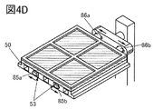
- 4B to 4D are diagrams illustrating a substrate reversing device and a substrate transfer jig.
- 5A to 5C are diagrams for explaining the substrate reversal operation.
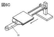
- 6A to 6C are diagrams for explaining the substrate reversal operation.
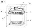
- FIG. 7A is a diagram illustrating a sputtering apparatus.
- FIG. 7A is a diagram illustrating a sputtering apparatus.
- FIG. 7B is a diagram illustrating a dry etching apparatus.
- 8A to 8D are diagrams illustrating a display device.
- 9A and 9B are diagrams illustrating a display device.
- 10A to 10D are diagrams illustrating a method of manufacturing a display device.
- 11A to 11D are views for explaining a method of manufacturing a display device.
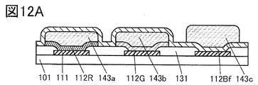
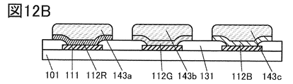
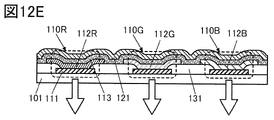
- 12A to 12E are diagrams illustrating a method of manufacturing a display device.
- FIG. 13 is a diagram illustrating a manufacturing apparatus.
- One aspect of the present invention is a manufacturing apparatus mainly used for forming a light emitting element (also referred to as a light emitting device) such as an organic EL element.
- a light emitting element also referred to as a light emitting device
- an organic EL element In order to miniaturize the organic EL element or increase the occupied area in the pixel, it is preferable to use a lithography process. However, if impurities such as water, oxygen, and hydrogen enter the organic EL element, the reliability is impaired, so it is necessary to take measures such as controlling the atmosphere from the manufacturing stage to a low dew point.
- the film forming step, the lithography step, the etching step, and the sealing step for forming the organic EL element can be continuously performed without opening to the atmosphere. Therefore, it is possible to form an organic EL element that is miniaturized and has high brightness and high reliability.
- FIG. 1 is a diagram illustrating a manufacturing apparatus for a light emitting device according to an aspect of the present invention.
- the manufacturing apparatus includes a load / unload unit 10, a vacuum control cluster 20, an atmosphere control cluster 30, and a load lock chamber 40.
- a group of devices for performing the main process under vacuum is referred to as a vacuum control cluster.
- a group of devices for performing the main process under atmosphere control is called an atmosphere control cluster.
- the load / unload unit 10 has a load / unload chamber LU (load / unload chamber LU1, LU2, LU3) and a transfer chamber TF1.
- the transfer chamber TF1 is connected to the load / unload chamber LU. Further, the transfer chamber TF1 is connected to the load lock chamber 40 via the gate valve 41.
- the transfer chamber TF1 is provided with a transfer device 70a, and the substrate installed in the load / unload chamber LU can be transported to the load lock chamber 40. Further, the atmosphere of the load / unload chamber LU may be controlled to an inert gas atmosphere in the same manner as the atmosphere control cluster 30 described later.
- load / unload chamber LU there may be a gate valve between the load / unload chamber LU and the transfer chamber TF1.
- load / unload chamber LU is shown as an example in FIG. 1, the load chamber and the unload chamber may be provided respectively.
- the vacuum control cluster 20 has a transfer chamber TF2 and a vacuum process device VC.
- FIG. 1 shows an example in which there are six vacuum process devices VC (vacuum process devices VC1 to VC6), but one or more may be used according to the purpose.
- a vacuum pump VP is connected to the vacuum process device VC, and a gate valve is provided between the vacuum process device VC and the transfer chamber TF2. Therefore, each vacuum process apparatus VC can perform a vacuum process such as film formation or etching in parallel.
- the vacuum process means processing in an environment controlled by depressurization. Therefore, the vacuum process includes not only the process under high vacuum but also the process of introducing a process gas to control the pressure.
- An independent vacuum pump VP is also provided in the transfer chamber TF2 to prevent cross-contamination in the process performed by the vacuum process apparatus VC.
- it may have a configuration in which a gate valve is not provided between the transfer chamber TF2 and the vacuum process apparatus VC6.
- the transfer chamber TF2 is connected to the load lock chamber 40 via the gate valve 42.
- a transfer device 70b is provided in the transfer chamber TF2, and the substrate installed in the load lock chamber 40 can be transferred to the vacuum process device VC.
- a film forming apparatus such as a vapor deposition apparatus, a sputtering apparatus, a CVD (Chemical Vapor Deposition) apparatus, and an ALD (Atomic Layer Deposition) apparatus can be applied.
- a thermal CVD apparatus using heat a PECVD apparatus using plasma (Plasma Enhanced CVD apparatus), or the like can be used.
- the ALD device a thermal ALD device using heat, a PEALD device using a plasma-excited reactor (Plasma Enhanced ALD device), or the like can be used.
- the etching apparatus a dry etching apparatus or the like can be applied.
- an auxiliary mechanism such as a substrate transfer jig attachment / detachment device and a substrate reversing device may be applied as the vacuum process device VC. It should be noted that these auxiliary mechanisms can be applied to a vacuum process device VC6 or the like in which a gate valve is not provided between the transfer chamber TF2 and the like.
- the atmosphere control cluster has a transfer chamber TF3 and a normal pressure process apparatus AC that mainly performs the process under normal pressure.
- FIG. 1 shows an example in which there are six normal pressure process devices AC (normal pressure process devices AC1 to AC6), one or more may be used depending on the purpose.
- the process is not limited to the process under normal pressure, and negative pressure or positive pressure slightly higher than normal pressure may be used. Further, when a plurality of normal pressure process devices AC are provided, the atmospheric pressure may be different for each.
- a valve for introducing the inert gas (IG) is connected to the transfer chamber TF3 and the atmospheric pressure process apparatus AC, and the atmosphere can be controlled to the inert gas atmosphere.
- the inert gas nitrogen or a noble gas such as argon or helium can be used.
- the inert gas preferably has a low dew point (for example, -50 ° or less).
- FIG. 1 shows an example in which each of the normal pressure process devices AC1 to AC5 is connected to the transfer chamber TF3 via a gate valve.
- a gate valve By providing a gate valve, it is possible to control the atmospheric pressure, control the type of inert gas, prevent cross-contamination, and the like. If these strict controls are not required, the transfer chamber TF3 may be connected to the transfer chamber TF3 without using a gate valve as in the normal pressure process device AC6.
- the transfer chamber TF3 is connected to the load lock chamber 40 via the gate valve 43.
- a transfer device 70c is provided in the transfer chamber TF3, and the substrate installed in the load lock chamber 40 can be transferred to the normal pressure process device AC.
- an apparatus for performing a lithography process can be applied.
- a resin (photoresist) coating device an exposure device, a developing device, a baking device, etc.
- resin UV curable resin, etc.
- a device, a nanoimprint device, or the like may be applied.
- a cleaning device, a wet etching device, a coating device, a resist stripping device, or the like may be applied to the normal pressure process device AC depending on the application.
- the load lock chamber 40 is provided with a vacuum pump VP and a valve for introducing the inert gas. Therefore, the load lock chamber 40 can be controlled to a reduced pressure or an inert gas atmosphere. For example, when the substrate is transferred from the vacuum control cluster 20 to the atmosphere control cluster 30, the substrate is carried in from the vacuum control cluster 20 with the load lock chamber 40 depressurized, the load lock chamber 40 is made into an inert gas atmosphere, and then the atmosphere control cluster. The operation of carrying out the substrate to 30 can be performed.
- the load lock chamber 40 is provided with a substrate rotation mechanism 45 for rotating the conveyed substrate about a Z axis (an axis perpendicular to the center of the upper surface of the substrate).
- a Z axis an axis perpendicular to the center of the upper surface of the substrate.
- the substrate can be easily carried in and out of the transfer chamber TF1 and the transfer chamber TF2 or the transfer chamber TF3 by rotating the substrate by 90 ° about the Z axis.
- the substrate rotation mechanism 45 can be omitted.
- the substrate is carried into the vacuum control cluster 20 from the load / unload chamber, and a film forming process is performed.
- the substrate is transferred from the vacuum control cluster 20 to the atmosphere control cluster 30, and a lithography process is performed.
- the substrate is transferred from the atmosphere control cluster 30 to the vacuum control cluster 20, and an etching process is performed to form a structure (light emitting element such as an organic EL element).
- a film forming step of forming a protective film covering the structure is performed by the vacuum control cluster 20.
- the substrate is carried out from the vacuum control cluster 20 to the load / unload chamber LU.
- the structure can be carried out into the atmosphere in a state of being sealed with a protective film without exposing the structure to the atmosphere. That is, when the organic EL element is formed as a structure, it is possible to suppress the invasion of impurities contained in the atmosphere and improve the reliability.
- ⁇ Board transfer jig> When performing a plurality of steps in the vacuum control cluster, the orientation (face-up or face-down) of the substrate to be installed may differ depending on the vacuum process apparatus VC. Therefore, it may be necessary to invert the substrate between processes.
- the substrate In the face-up method, the substrate can be transported by placing it on the hand portion of the transport device with the surface of the substrate forming the structure as the upper surface. Therefore, it is easy to install it on a stage (electrode or the like) in the vacuum process apparatus VC.
- a stage electrode or the like
- the substrate when the substrate is installed in the vacuum process apparatus VC, it is held near the edge of the substrate. When the substrate is small, these problems can be avoided only by holding near the edge of the substrate, but since the substrate bends in a large substrate, it is difficult to transport and install the substrate alone.
- FIGS. 2A and 2B it is preferable to use a substrate transfer jig as shown in FIGS. 2A and 2B.
- the substrate transfer jig has a jig 51 and a jig 54.
- FIG. 2A is a diagram in which the substrate 60 is mounted on a substrate transfer jig, and in the present specification, the configuration is referred to as a work substrate 50.
- the jig 54 has an opening, and the other portion is a region necessary for holding the substrate 60. Since a product such as a light emitting element is formed in an opening, the size and shape of the opening may be adjusted according to the purpose.
- FIG. 2B is a diagram in which the jig 51, the substrate 60, and the jig 54 are separated into upper and lower parts.
- the jig 51 and the jig 54 are preferably formed of a hard material such as metal, ceramics, or cermet. Alternatively, these may be combined and formed.
- FIG. 2B shows an example in which a magnet 55 is provided on a jig 51 and a substrate 60 is sandwiched between jigs 54 made of magnetic metal.
- the magnetic metal may be provided only on the portion of the jig 54 facing the magnet 55, and the other portion may be formed by ceramics or the like.
- the magnet 55 may be provided on the jig 54 side.
- the magnet 55 may be provided on both the jig 51 and the jig 54.
- the substrate 60 may be sandwiched between the jig 51 and the jig 54 by using a spring or other configuration.
- the jig 51 has a shape corresponding to the shape of the substrate 60, and when the upper surface shape of the substrate 60 is rectangular, the upper surface shape of the jig 51 is also rectangular, and it is preferable that the size is equal to or larger than that of the substrate 60.
- the jig 51 having a rectangular upper surface has a flat plate portion, and has a first end portion perpendicular to the upper surface of the flat plate portion and a second end portion facing the first end portion. Is provided with a convex portion 56.
- the convex portion 56 can be used at the time of face-down installation described later.
- a through hole 52 and a through hole 53 are provided between the third end portion perpendicular to the first end portion and the fourth end portion facing the third end portion.
- FIG. 3B a comparison of the sizes of the through hole 52 and the hand portion 71 of the transport device 70 (conveyor devices 70a to 70c) is shown in FIG. 3B.
- the inner dimension of the cross section perpendicular to the long axis of the through hole 52 is X1 ⁇ Y1
- the outer dimension of the cross section perpendicular to the long axis of the hand portion 71 is X2 ⁇ Y2, X1> X2 and Y1> Y2. Therefore, as shown in FIG. 3A, the hand portion 71 of the transport device 70 can be inserted into the through hole 52.
- the hand portion 71 of the transport device 70 can be inserted into the through hole 52 for transport. Therefore, since the hand portion 71 does not touch the surface of the substrate 60 and the jig 54, it is possible to prevent scratches and contamination on the surface of the substrate 60, and to prevent the film adhering to the jig 54 from peeling off.
- the through hole of the hand portion 71 of the transport device 70 with respect to the fixed work substrate 50. Insertion and extraction to and from 52 can be performed only by the operation of the transport device 70. Therefore, in the vacuum process apparatus VC or the like, the pusher pin for lifting the substrate or the like can be eliminated.
- the number of through holes 52 is 3, but it may be 2 or 4 or more.
- the through hole 53 is a through hole for inserting the hand portions 85a and 85b of the substrate reversing device 80 shown in FIG. 4A.
- the substrate reversing device 80 has a pillar 82 fixed to the gantry 81, a rotation mechanism 83 fixed to the pillar 82, and a rotating portion 84 fixed to the rotation shaft of the rotation mechanism 83.
- the rotating portion 84 has horizontal moving mechanisms 86a and 86b, the hand portion 85a is connected to the horizontal moving mechanism 86a, and the hand portion 85b is connected to the horizontal moving mechanism 86b.
- FIG. 4B shows a cross section perpendicular to the long axis of the hand portion 85b of the substrate reversing device 80 and a cross section perpendicular to the long axis of the through hole 53.
- the cross section of the hand portion 85b perpendicular to the long axis has a partially convex shaped portion 87.
- the cross section perpendicular to the long axis of the through hole 53 has a concave shaped portion 57 in part.
- the hand portions 85a and 85b and the work board 50 can be fixed by moving the hand portion 85b having a line-symmetrical configuration in the same manner.
- the convex shape portion 87 and the concave shape portion 57 may have a shape as long as they are in close contact with each other and may have a curvature.
- the work board 50 is on standby with the hand portion 71 of the transport device 70 inserted into the through hole 52 in advance. Further, it is assumed that the surface of the substrate 60 is the upper surface.
- the hand portion 85a and the hand portion 85b of the substrate reversing device 80 are moved in a direction approaching each other, and the transfer device 70 is operated so that the hand portion 85a and the hand portion 85b are inserted into the through hole 53 (see FIG. 5A). ..
- the hand portion 85a and the hand portion 85b are moved in a direction away from each other, and the work substrate 50 is fixed to the hand portion 85a and the hand portion 85b. Then, the hand portion 71 of the transport device 70 is slightly lowered to a height that does not contact the inner wall of the through hole 52 (see FIG. 5B). Then, the hand portion 71 is pulled out from the through hole 52 (see FIG. 5C).
- the rotating portion 84 is rotated by the rotating mechanism 83 (see FIG. 6A), and after inversion, the hand portion 71 of the transport device is inserted into the through hole 52.
- the hand portion 85a and the hand portion 85b of the substrate reversing device 80 are moved in a direction approaching each other, and the fixing of the hand portion 85a and the hand portion 85b and the work substrate 50 is released.
- the hand portion 71 of the transport device 70 is slightly raised to a height in contact with the inner wall of the through hole 52 (see FIG. 6B).
- the hand portion 71 is retracted, and the work substrate 50 is pulled out from the hand portion 85a and the hand portion 85b of the substrate reversing device 80.
- the above is the reversing operation of the work board 50.
- the same operation may be performed when returning from the state of FIG. 6C to the state of FIG. 5A.
- FIG. 7A is a diagram illustrating a vacuum process device VC in which the work substrate 50 is installed face-down, and here exemplifies a sputtering device 90a.
- the chamber is shown by a broken line and the gate valve is omitted.
- the sputtering apparatus 90a has a pair of rails 91 fixed to the chamber between the cathode 92 (target) and the anode 93. By installing the work substrate 50 so that the side surface of the convex portion 56 of the work substrate 50 rests on the rail 91, the work substrate 50 can be installed face-down in the chamber of the sputtering apparatus 90a.
- a vertical mechanism for raising and lowering the anode 93 may be provided.
- the anode 93 can be brought into contact with the work substrate 50 by the vertical mechanism, and bias application to the work substrate 50 and / or heating by a heater provided on the anode 93 can be efficiently performed.
- the thin-film deposition apparatus for installing the work substrate 50 face-down can also be configured to install the work substrate 50 on the rail 91 in the same manner as the sputtering apparatus 90a shown in FIG. 7A.
- FIG. 7B is a diagram illustrating a vacuum process apparatus VC in which the work substrate 50 is installed face-up, and here exemplifies a dry etching apparatus 90b.
- the chamber is shown by a broken line and the gate valve is omitted.
- the dry etching apparatus 90b has a parallel plate type cathode 95 (stage) and an anode 96.
- a CVD device, an ALD device, or the like on which the work board 50 is installed face-up can also be configured to install the work board 50 on the stage in the same manner as the dry etching device 90b shown in FIG. 7B.
- the film forming step, the lithography step, the etching step, and the sealing step can be continuously performed without opening to the atmosphere. Therefore, it is possible to form an organic EL element that is miniaturized and has high brightness and high reliability.
- a metal mask or a device manufactured by using an FMM may be referred to as a device having an MM (metal mask) structure.
- a device manufactured without using a metal mask or FMM may be referred to as a device having an MML (metal maskless) structure.
- SBS Side
- a light emitting device capable of emitting white light may be referred to as a white light emitting device.
- the white light emitting device can be combined with a colored layer (for example, a color filter) to form a full color display light emitting device.
- the light emitting device can be roughly classified into a single structure and a tandem structure.
- a device having a single structure preferably has one light emitting unit between a pair of electrodes, and the light emitting unit is preferably configured to include one or more light emitting layers.
- a light emitting layer may be selected so that the light emission of each of the two or more light emitting layers has a complementary color relationship. For example, by making the emission color of the first light emitting layer and the emission color of the second light emitting layer have a complementary color relationship, it is possible to obtain a configuration in which the entire light emitting device emits white light. The same applies to a light emitting device having three or more light emitting layers.
- the device having a tandem structure preferably has two or more light emitting units between a pair of electrodes, and each light emitting unit is preferably configured to include one or more light emitting layers.
- each light emitting unit is preferably configured to include one or more light emitting layers.
- the light emitted from the light emitting layers of a plurality of light emitting units may be combined to obtain white light emission.
- the configuration for obtaining white light emission is the same as the configuration for a single structure.
- the SBS structure light emitting device can have lower power consumption than the white light emitting device.
- the white light emitting device is suitable because the manufacturing process is simpler than that of the light emitting device having an SBS structure, so that the manufacturing cost can be lowered or the manufacturing yield can be increased.
- the device having a tandem structure may have a configuration (BB, GG, RR, etc.) having a light emitting layer that emits light of the same color.
- the tandem structure in which light emission is obtained from a plurality of layers requires a high voltage for light emission, but the current value for obtaining the same light emission intensity as that in the single structure is small. Therefore, in the tandem structure, the current stress per light emitting unit can be reduced, and the device life can be extended.
- FIG. 8A shows a schematic top view of the display device 100 according to one aspect of the present invention.
- the display device 100 has a plurality of light emitting elements 110R exhibiting red, a light emitting element 110G exhibiting green, and a plurality of light emitting elements 110B exhibiting blue.
- R, G, and B are designated in the light emitting region of each light emitting element in order to easily distinguish each light emitting element.
- the light emitting element 110R, the light emitting element 110G, and the light emitting element 110B are arranged in a matrix.
- FIG. 8A shows a so-called stripe arrangement in which light emitting elements of the same color are arranged in one direction.
- the arrangement method of the light emitting elements is not limited to this, and an arrangement method such as a delta arrangement or a zigzag arrangement may be applied, or a pentile arrangement may be used.
- an EL element such as an OLED (Organic Light Emitting Diode) or a QLED (Quantum-dot Light Emitting Diode).
- the light emitting substances possessed by the EL element include substances that emit fluorescence (fluorescent material), substances that emit phosphorescence (phosphorescent material), inorganic compounds (quantum dot material, etc.), and substances that exhibit thermal activated delayed fluorescence (thermally activated delayed fluorescence). (Themally activated delayed fluorescence (TADF) material) and the like.
- FIG. 8B is a schematic cross-sectional view corresponding to the alternate long and short dash line A1-A2 in FIG. 8A
- FIG. 8C is a schematic cross-sectional view corresponding to the alternate long and short dash line B1-B2.
- FIG. 8A shows a cross section of the light emitting element 110R, the light emitting element 110G, and the light emitting element 110B.
- the light emitting element 110R, the light emitting element 110G, and the light emitting element 110B are each provided on the substrate 101 and have a pixel electrode 111 and a common electrode 113.
- the light emitting element 110R has an EL layer 112R between the pixel electrode 111 and the common electrode 113.
- the EL layer 112R has a luminescent organic compound that emits light having a peak in at least the red wavelength region.
- the EL layer 112G included in the light emitting device 110G has a luminescent organic compound that emits light having a peak in at least a green wavelength region.
- the EL layer 112B included in the light emitting device 110B has a luminescent organic compound that emits light having a peak in at least a blue wavelength region.
- the EL layer 112R, the EL layer 112G, and the EL layer 112B are composed of an electron injection layer, an electron transport layer, a hole injection layer, and a hole transport layer, in addition to a layer (light emitting layer) containing a luminescent organic compound, respectively. Of these, one or more may be possessed.
- the pixel electrode 111 is provided for each light emitting element. Further, the common electrode 113 is provided as a continuous layer common to each light emitting element. A conductive film having transparency to visible light is used for either the pixel electrode 111 or the common electrode 113, and a conductive film having reflection to visible light is used for the other.
- a bottom injection type (bottom emission type) display device By making the pixel electrode 111 translucent and the common electrode 113 reflective, it is possible to make a bottom injection type (bottom emission type) display device.
- a top-emission type (top emission type) display device can be obtained.
- By making both the pixel electrode 111 and the common electrode 113 translucent it is possible to make a double-sided injection type (dual emission type) display device. In this embodiment, an example of manufacturing a top injection type (top emission type) display device and a bottom injection type (bottom emission type) display device will be described.
- An insulating layer 131 is provided so as to cover the end portion of the pixel electrode 111.
- the end portion of the insulating layer 131 preferably has a tapered shape.
- the EL layer 112R, the EL layer 112G, and the EL layer 112B each have a region in contact with the upper surface of the pixel electrode 111 and a region in contact with the surface of the insulating layer 131. Further, the ends of the EL layer 112R, the EL layer 112G, and the EL layer 112B are located on the insulating layer 131.
- a gap is provided between the two EL layers between the light emitting elements of different colors.
- the EL layer 112R, the EL layer 112G, and the EL layer 112B are provided so as not to be in contact with each other. As a result, it is possible to suitably prevent unintended light emission due to current flowing through the two EL layers adjacent to each other. Therefore, the contrast can be enhanced, and a display device with high display quality can be realized.
- FIG. 8C shows an example in which the EL layer 112G is processed into an island shape.
- the EL layer 112G may be processed into a strip shape so that the EL layer 112G is continuous in the column direction.
- the space required for dividing the EL layer 112G or the like is not required, and the area of the non-light emitting region between the light emitting elements can be reduced, so that the aperture ratio can be increased.
- the cross section of the light emitting element 110G is shown as an example in FIGS. 8C and 8D, the light emitting element 110R and the light emitting element 110B can have the same shape.
- a protective layer 121 is provided so as to cover the light emitting element 110R, the light emitting element 110G, and the light emitting element 110B.
- the protective layer 121 has a function of preventing impurities from diffusing into each light emitting element from above.
- the protective layer 121 may have, for example, a single-layer structure or a laminated structure including at least an inorganic insulating film.
- the inorganic insulating film include an oxide film such as a silicon oxide film, a silicon nitride film, a silicon nitride film, a silicon nitride film, an aluminum oxide film, an aluminum nitride film, and a hafnium oxide film, or a nitride film. ..
- a semiconductor material such as indium gallium oxide or indium gallium zinc oxide may be used as the protective layer 121.
- FIGS. 8A to 8D illustrate, but are not limited to, configurations in which the light emitting layers of the light emitting elements of R, G, and B are different from each other.
- an EL layer 112W that emits white light is provided, and colored layers 114R (red), 114G (green), and 114B are provided so as to be superimposed on the EL layer 112W to provide a light emitting element 110R.
- a method of forming 110G and 110B and colorizing them may be used.
- FIG. 9A is an example of a top emission type display device
- FIG. 9B is an example of a bottom emission display device.
- the EL layer 112W can have, for example, a tandem structure in which the EL layers that emit light of each of R, G, and B are connected in series. Alternatively, a structure in which light emitting layers that emit light of each of R, G, and B are connected in series may be used.
- the colored layers 114R, 114G, and 114B for example, red, green, and blue color filters can be used.
- the thin film (insulating film, semiconductor film, conductive film, etc.) constituting the display device is formed by using a sputtering method, a chemical vapor deposition (CVD) method, a vacuum vapor deposition method, an atomic layer deposition (ALD) method, or the like. be able to.
- the CVD method include a plasma chemical vapor deposition (PECVD: Plasma Enhanced CVD) method and a thermal CVD method.
- PECVD plasma chemical vapor deposition
- thermal CVD there is an organometallic chemical vapor deposition (MOCVD: Metalorganic CVD) method.
- MOCVD Metalorganic CVD
- spin coating, dip, spray coating, inkjet, dispense, screen printing, offset printing, etc. are used to form thin films (insulating films, semiconductor films, conductive films, etc.) that make up display devices and to apply resins and the like used in lithography processes.
- a method such as a doctor knife method, a slit coat, a roll coat, a curtain coat, or a knife coat can be used.
- an apparatus for forming a thin film by the above method can be used.
- an apparatus for applying the resin by the above method can be used.
- the thin film when processing the thin film constituting the display device, a photolithography method or the like can be used.
- the thin film may be processed by using the nanoimprint method.
- a method of directly forming an island-shaped thin film by a film forming method using a shielding mask may be used in combination.
- a thin film processing method using a photolithography method there are typically the following two methods.
- One is a method of forming a resist mask on a thin film to be processed, processing the thin film by etching or the like, and removing the resist mask.
- the other is a method in which a photosensitive thin film is formed, and then exposed and developed to process the thin film into a desired shape.
- the light used for exposure for example, i-line (wavelength 365 nm), g-line (wavelength 436 nm), h-line (wavelength 405 nm), or a mixture thereof can be used.
- ultraviolet rays, KrF laser light, ArF laser light, or the like can also be used.
- the exposure may be performed by the immersion exposure technique.
- extreme ultraviolet (EUV: Extreme Ultra-violet) light or X-rays may be used.
- an electron beam can be used instead of the light used for exposure. It is preferable to use extreme ultraviolet light, X-rays or an electron beam because extremely fine processing is possible.
- extreme ultraviolet light, X-rays or an electron beam because extremely fine processing is possible.
- a dry etching method, a wet etching method, or the like can be used for etching the thin film.
- an apparatus for processing a thin film by the above method can be used.
- a substrate having at least enough heat resistance to withstand the subsequent heat treatment can be used.
- a glass substrate, a quartz substrate, a sapphire substrate, a ceramic substrate, an organic resin substrate, or the like can be used.
- a single crystal semiconductor substrate made of silicon, silicon carbide or the like, a polycrystalline semiconductor substrate, a compound semiconductor substrate such as silicon germanium, or a semiconductor substrate such as an SOI substrate can be used.
- the substrate 101 it is preferable to use a substrate in which a semiconductor circuit including a semiconductor element such as a transistor is formed on the semiconductor substrate or an insulating substrate.
- the semiconductor circuit preferably comprises, for example, a pixel circuit, a gate line drive circuit (gate driver), a source line drive circuit (source driver), or the like.
- gate driver gate line drive circuit
- source driver source driver
- an arithmetic circuit, a storage circuit, or the like may be configured.
- a plurality of pixel electrodes 111 are formed on the substrate 101.
- a conductive film to be a pixel electrode 111 is formed, a resist mask is formed by a photolithography method, and an unnecessary portion of the conductive film is removed by etching. After that, the pixel electrode 111 can be formed by removing the resist mask.
- a material for example, silver or aluminum
- the pixel electrode 111 made of the material can be said to be an electrode having light reflectivity.
- the pixel electrode 111 is made of one or more materials having the highest possible transmittance in the entire wavelength range of visible light (for example, indium tin oxide, or indium, gallium, zinc, etc.). It is preferable to apply (including oxides, etc.). Further, the surface of the pixel electrode 111 may have a thin metal film (for example, an alloy of silver and magnesium) that transmits light emitted from the light emitting layer.
- the pixel electrode 111 made of the material can be said to be an electrode having light transmittance. As a result, not only the light extraction efficiency of the light emitting element can be improved, but also the color reproducibility can be improved.
- the end portion of the pixel electrode 111 is covered to form the insulating layer 131 (see FIG. 10A).
- the insulating layer 131 an organic insulating film or an inorganic insulating film can be used.
- the insulating layer 131 preferably has a tapered end portion in order to improve the step covering property of the later EL film.
- it is preferable to use a photosensitive material because it is easy to control the shape of the end portion depending on the exposure and development conditions.
- the EL film 112Rf has a film containing at least a red-emitting organic compound.
- the electron injection layer, the electron transport layer, the charge generation layer, the hole transport layer, and the hole injection layer may be laminated.
- the EL film 112Rf can be formed by, for example, a vapor deposition method, a sputtering method, or the like. Not limited to this, the above-mentioned film forming method can be appropriately used.
- a resist mask 143a is formed on the pixel electrode 111 corresponding to the light emitting element 110R (see FIG. 10C).
- the resist mask 143a can be formed by a lithography process.
- the EL film 112Rf is etched using the resist mask 143a as a mask to form the EL layer 112R in an island shape (see FIG. 10D).
- a dry etching method or a wet etching method can be used for the etching step.
- an EL film 112Gf which will later become an EL layer 112G, is formed on the exposed pixel electrodes 111 and the insulating layer 131, and on the resist mask 143a (see FIG. 11A).
- the EL film 112Gf has a film containing at least a green luminescent organic compound.
- the electron injection layer, the electron transport layer, the charge generation layer, the hole transport layer, and the hole injection layer may be laminated.
- a resist mask 143b is formed on the pixel electrode 111 corresponding to the light emitting element 110G (see FIG. 11B).
- the resist mask 143b can be formed by a lithography process.
- the EL film 112Gf is etched using the resist mask 143b as a mask to form the EL layer 112G in an island shape (see FIG. 11C).
- a dry etching method or a wet etching method can be used for the etching step.
- an EL film 112Bf which will later become the EL layer 112B, is formed on the exposed pixel electrodes 111 and the insulating layer 131, and on the resist mask 143a and the resist mask 143b (see FIG. 11D).
- the EL film 112Bf has a film containing at least a blue light emitting organic compound.
- the electron injection layer, the electron transport layer, the charge generation layer, the hole transport layer, and the hole injection layer may be laminated.
- a resist mask 143c is formed on the pixel electrode 111 corresponding to the light emitting element 110B (see FIG. 12A).
- the resist mask 143b can be formed by a lithography process.
- the EL film 112Bf is etched using the resist mask 143c as a mask to form the EL layer 112B in an island shape (see FIG. 12B).
- a dry etching method or a wet etching method can be used for the etching step.
- ⁇ Resist mask removal> Subsequently, the resist mask 143a, the resist mask 143b, and the resist mask 143c are removed (see FIG. 12C).
- a peeling method using an organic solvent can be used.
- ashing using a dry etching apparatus may be used.
- a conductive film serving as a common electrode 113 of the organic EL element is formed on the EL layer 112R, the EL layer 112G, the EL layer 112B, and the insulating layer 131 exposed in the previous step.
- a thin-film deposition device and / or a sputtering device can be used in the step of forming the conductive film to be the common electrode 113.
- the common electrode 113 When manufacturing a top-emission type display device, the common electrode 113 includes a thin metal film (for example, an alloy of silver and magnesium) that transmits light emitted from a light emitting layer, a translucent conductive film (for example, indium tin oxide, etc.). Alternatively, any single film (such as an oxide containing one or more of indium, gallium, and zinc) or a laminated film of both can be used. The common electrode 113 made of such a film can be said to be an electrode having light transmittance.
- a thin metal film for example, an alloy of silver and magnesium
- a translucent conductive film for example, indium tin oxide, etc.
- any single film such as an oxide containing one or more of indium, gallium, and zinc
- the common electrode 113 made of such a film can be said to be an electrode having light transmittance.
- the electrode having light reflectivity as the pixel electrode 111 and having the electrode having light transmission as the common electrode 113 the light emitted from the light emitting layer can be emitted to the outside through the common electrode 113. That is, a top emission type light emitting element is formed.
- the common electrode 113 When manufacturing a bottom emission type display device, it is preferable to use a material (for example, silver or aluminum) having as high a reflectance as possible in the entire wavelength range of visible light as the common electrode 113.
- the common electrode 113 formed of the material can be said to be an electrode having light reflectivity.
- the electrode having light transmittance as the pixel electrode 111 and having the electrode having light reflection property as the common electrode 113 the light emitted from the light emitting layer can be emitted to the outside through the pixel electrode 111. That is, a bottom emission type light emitting element is formed.
- the protective layer 121 is formed on the common electrode 113 (see FIGS. 12D and 12E).
- a sputtering device, a CVD device, an ALD device, or the like can be used in the step of forming the protective layer.
- FIG. 12D shows a top emission type display device
- FIG. 12E shows a bottom emission type display device.
- FIG. 13 shows an example of a manufacturing apparatus that can be used in the manufacturing process from the formation of the EL film 112Rf to the formation of the protective layer 121 described above.
- the basic configuration of the manufacturing apparatus shown in FIG. 13 is the same as that of the manufacturing apparatus shown in FIG. An example of embodying the device is shown.
- FIG. 13 is a perspective view schematically showing the entire manufacturing apparatus, and the utility, the gate valve, and the like are not shown. Further, the transfer chambers TF1, TF2, TF3, TF4, and the load lock chamber 40 are shown as a visualization of the inside for clarification.
- the vacuum control cluster 20 has a block having a transfer chamber TF2 and vacuum process devices VC1 to VC11, and a block having a transfer chamber TF4 and vacuum process devices VC12 to VC14.
- the transfer chamber TF2 and the vacuum process devices VC1 to VC14 may be formed as one block without dividing the vacuum control cluster into two blocks.
- the transfer chamber TF2 has a transfer device 70b.
- the transfer chamber TF4 has a transfer device 70d.
- the transport device 70b is self-propelled and can move on the rail 75.
- the vacuum process devices VC1 to VC5 are vapor deposition devices for forming the EL film 112Rf, the EL film 112Gf, and the EL film 112Bf.
- each of the vacuum process devices VC2, VC3, and VC4 can be used as a forming device for the light emitting layer (R), the light emitting layer (G), and the light emitting layer (B).
- the vacuum process devices VC1 and VC5 can be assigned to forming devices such as an electron injection layer, an electron transport layer, a charge generation layer, a hole transport layer, and a hole injection layer, which are common layers.
- the vacuum process device VC6 can be a board transfer jig attachment / detachment device described with reference to FIGS. 2A and 2B.
- the transfer device 70b can also transfer a single substrate, and can carry the substrate into the vacuum process device VC6 and attach the substrate transfer jig. Further, the substrate transfer jig can be removed by the vacuum process device VC6, and the substrate alone can be carried out.
- the vacuum process apparatus VC7 can be the substrate reversing apparatus described with reference to FIGS. 4A to 4C.
- the work substrate 50 can be inverted as needed by the vacuum process apparatus VC7.
- the vacuum process devices VC8 and VC9 can be a film forming device that forms the common electrode 113.
- the vacuum process apparatus VC8 can be a vapor deposition apparatus used for forming a metal film that transmits visible light.
- the vacuum process apparatus VC9 can be a sputtering apparatus used for forming a translucent conductive film.
- the vacuum process device VC10 can be a film forming device that forms the protective layer 121.
- the vacuum process device VC10 can be a sputtering device. Alternatively, it may be a CVD device, an ALD device, or the like. Alternatively, a plurality of these film forming devices may be provided as another vacuum process device VC, and the protective layer 121 may be formed of a laminated film.
- the vacuum process apparatus VC11 can be a dry etching apparatus that forms the EL layer 112R, the EL layer 112G, and the EL layer 112B, and removes the resist mask.
- an ashing device may be provided as another vacuum process device VC.
- One or more of the vacuum process devices VC12, VC13, and VC14 can be vacuum bake devices. Since the reliability of an organic EL element deteriorates due to the intrusion of impurities such as water, vacuum baking (heat treatment under reduced pressure) is performed as a step before forming the EL film 112Rf, EL film 112Gf, and EL film 112Bf, and the work is performed. It is preferable to remove impurities such as water adhering to the substrate 50.
- vacuum process devices VC12, VC13, and VC14 can all be vacuum bake devices.
- the atmosphere control cluster 30 has a transfer chamber TF3 and atmospheric pressure process devices AC1 to AC8.
- the transfer chamber TF3 has a transfer device 70c.
- the transport device 70c is self-propelled and can move on the rail 75.
- ⁇ AC1, AC2, AC3> Any one or more of a cleaning device, a wet etching device, a resist stripping device, and the like can be assigned to the normal pressure process devices AC1 to AC3. It may be appropriately selected according to the process.
- the normal pressure process devices AC1 to AC9 can be devices used in the lithography process.
- the normal pressure process device AC1 can be used as a resin (photoresist) coating device
- the normal pressure process device AC2 can be used as an exposure device
- the normal pressure process device AC3 can be used as a developing device.
- the normal pressure process device AC1 can be used as a resin (UV curable resin or the like) coating device
- the normal pressure process device AC2 can be used as a nanoimprint device
- the normal pressure process device AC3 can be used as a developing device. If the developing device is not used, another device may be assigned to the normal pressure process device AC3.
- the normal pressure process devices AC7 to AC9 can be bake devices.
- the baking device can pre-bake, post-bake, or post-wash the photoresist.
- Tables 1 and 2 summarize the processes and processing devices using the manufacturing apparatus shown in FIG. 13, the front and back surfaces of the substrate (up: face-up method, down: face-down method), and the elements corresponding to the above-mentioned manufacturing method.
- the description of the loading and unloading of the substrate into the load lock chamber 40 and each device is omitted.
- Table 1 shows a step after forming the pixel electrode 111 and before forming one kind of EL layer. Since the EL layer is formed by performing the relevant steps for each of R, G, and B, No. 1 in Table 1 is formed. 1 to No. The steps up to 16 will be performed three times.
- step No. The replacement of the substrate transfer jig of 55 is performed in step No. It may be replaced with a jig 54 having an opening larger than the opening of the jig 54 worn in 50. This makes it possible to provide a protective layer that covers the ends of the common electrodes.
- the manufacturing apparatus has the step No. 1 shown in Table 1. Step Nos. 1 to 2 shown in Table 2. It has a function to automatically perform up to 59.
- AC normal pressure process equipment
- AC1 normal pressure process equipment
- AC2 normal pressure process equipment
- AC3 normal pressure process equipment
- AC5 normal pressure process equipment
- AC6 normal pressure process equipment
- AC7 normal pressure process equipment
- AC8 Normal pressure process device
- AC9 Normal pressure process device
- LU Load unload chamber
- LU1 Load unload chamber
- LU2 Load unload chamber
- LU3 Load unload chamber
- TF1 Transfer chamber
- TF2 Transfer chamber
- TF3 Transfer chamber
- TF4 Transfer chamber
- VC Vacuum process equipment
- VC1 Vacuum process equipment
- VC2 Vacuum process equipment
- VC3 Vacuum process equipment
- VC4 Vacuum process equipment
- VC5 Vacuum process equipment
- VC6 Vacuum Process equipment
- VC7 Vacuum process equipment
- VC8 Vacuum process equipment
- VC9 Vacuum process equipment
- VC10 Vacuum process equipment
Landscapes
- Chemical & Material Sciences (AREA)
- Engineering & Computer Science (AREA)
- Physics & Mathematics (AREA)
- Manufacturing & Machinery (AREA)
- General Physics & Mathematics (AREA)
- Materials Engineering (AREA)
- Chemical Kinetics & Catalysis (AREA)
- Mechanical Engineering (AREA)
- Metallurgy (AREA)
- Organic Chemistry (AREA)
- Optics & Photonics (AREA)
- Inorganic Chemistry (AREA)
- General Chemical & Material Sciences (AREA)
- Electroluminescent Light Sources (AREA)
Priority Applications (2)
| Application Number | Priority Date | Filing Date | Title |
|---|---|---|---|
| US18/037,373 US20230422592A1 (en) | 2020-12-07 | 2021-11-25 | Manufacturing equipment of light-emitting device |
| JP2022567711A JPWO2022123381A1 (https=) | 2020-12-07 | 2021-11-25 |
Applications Claiming Priority (4)
| Application Number | Priority Date | Filing Date | Title |
|---|---|---|---|
| JP2020202402 | 2020-12-07 | ||
| JP2020-202402 | 2020-12-07 | ||
| JP2020-202401 | 2020-12-07 | ||
| JP2020202401 | 2020-12-07 |
Publications (1)
| Publication Number | Publication Date |
|---|---|
| WO2022123381A1 true WO2022123381A1 (ja) | 2022-06-16 |
Family
ID=81974212
Family Applications (1)
| Application Number | Title | Priority Date | Filing Date |
|---|---|---|---|
| PCT/IB2021/060951 Ceased WO2022123381A1 (ja) | 2020-12-07 | 2021-11-25 | 発光デバイスの製造装置 |
Country Status (3)
| Country | Link |
|---|---|
| US (1) | US20230422592A1 (https=) |
| JP (1) | JPWO2022123381A1 (https=) |
| WO (1) | WO2022123381A1 (https=) |
Families Citing this family (1)
| Publication number | Priority date | Publication date | Assignee | Title |
|---|---|---|---|---|
| WO2022137022A1 (ja) * | 2020-12-25 | 2022-06-30 | 株式会社半導体エネルギー研究所 | 表示装置の製造装置 |
Citations (6)
| Publication number | Priority date | Publication date | Assignee | Title |
|---|---|---|---|---|
| JPH09293589A (ja) * | 1996-04-26 | 1997-11-11 | Pioneer Electron Corp | 有機elディスプレイの製造方法 |
| JP2003264071A (ja) * | 2002-03-08 | 2003-09-19 | Ulvac Japan Ltd | 有機el素子の製造方法及びその装置 |
| JP2009170336A (ja) * | 2008-01-18 | 2009-07-30 | Sony Corp | 表示装置の製造方法 |
| JP2009170282A (ja) * | 2008-01-17 | 2009-07-30 | Seiko Epson Corp | 基板処理装置および有機エレクトロルミネッセンス装置の製造方法 |
| JP2011518252A (ja) * | 2008-03-05 | 2011-06-23 | アプライド マテリアルズ インコーポレイテッド | 回転モジュールを備えたコーティング装置 |
| JP2013065830A (ja) * | 2011-09-02 | 2013-04-11 | Canon Inc | 有機el装置 |
Family Cites Families (17)
| Publication number | Priority date | Publication date | Assignee | Title |
|---|---|---|---|---|
| TW318258B (https=) * | 1995-12-12 | 1997-10-21 | Tokyo Electron Co Ltd | |
| US5817366A (en) * | 1996-07-29 | 1998-10-06 | Tdk Corporation | Method for manufacturing organic electroluminescent element and apparatus therefor |
| JP3762255B2 (ja) * | 2001-06-05 | 2006-04-05 | 大日本印刷株式会社 | エレクトロルミネッセント素子の製造方法 |
| TWI258317B (en) * | 2002-01-25 | 2006-07-11 | Semiconductor Energy Lab | A display device and method for manufacturing thereof |
| JP4252317B2 (ja) * | 2003-01-10 | 2009-04-08 | 株式会社半導体エネルギー研究所 | 蒸着装置および蒸着方法 |
| JP4426190B2 (ja) * | 2003-01-24 | 2010-03-03 | 大日本印刷株式会社 | エレクトロルミネッセント素子の製造方法 |
| US7002292B2 (en) * | 2003-07-22 | 2006-02-21 | E. I. Du Pont De Nemours And Company | Organic electronic device |
| EP2098608A1 (en) * | 2008-03-05 | 2009-09-09 | Applied Materials, Inc. | Coating apparatus with rotation module |
| JP5361002B2 (ja) * | 2010-09-01 | 2013-12-04 | 独立行政法人産業技術総合研究所 | デバイス製造装置および方法 |
| JP6232655B2 (ja) * | 2011-09-02 | 2017-11-22 | 株式会社Joled | 有機el表示パネルおよびその製造方法 |
| TWI501861B (zh) * | 2011-12-06 | 2015-10-01 | 私立中原大學 | 滾輪式壓印系統 |
| WO2014116681A2 (en) * | 2013-01-22 | 2014-07-31 | Brooks Automation, Inc. | Substrate transport |
| CN105705997B (zh) * | 2013-11-08 | 2020-01-17 | Asml荷兰有限公司 | 生成用于定向自组装的引导模板的方法 |
| KR20150112348A (ko) * | 2014-03-27 | 2015-10-07 | 엘지디스플레이 주식회사 | 복사열 반사부를 가지는 진공 챔버 및 이를 이용한 유기 발광 표시 장치의 제조 방법 |
| US9536759B2 (en) * | 2015-05-29 | 2017-01-03 | Taiwan Semiconductor Manufacturing Co., Ltd | Baking apparatus and method |
| WO2017130440A1 (ja) * | 2016-01-26 | 2017-08-03 | 鴻海精密工業股▲ふん▼有限公司 | 蒸着マスク、その製造方法及びその蒸着マスクを使った有機発光ダイオードの製造方法 |
| US20200381276A1 (en) * | 2019-05-31 | 2020-12-03 | Applied Materials, Inc. | Multisubstrate process system |
-
2021
- 2021-11-25 WO PCT/IB2021/060951 patent/WO2022123381A1/ja not_active Ceased
- 2021-11-25 US US18/037,373 patent/US20230422592A1/en active Pending
- 2021-11-25 JP JP2022567711A patent/JPWO2022123381A1/ja not_active Withdrawn
Patent Citations (6)
| Publication number | Priority date | Publication date | Assignee | Title |
|---|---|---|---|---|
| JPH09293589A (ja) * | 1996-04-26 | 1997-11-11 | Pioneer Electron Corp | 有機elディスプレイの製造方法 |
| JP2003264071A (ja) * | 2002-03-08 | 2003-09-19 | Ulvac Japan Ltd | 有機el素子の製造方法及びその装置 |
| JP2009170282A (ja) * | 2008-01-17 | 2009-07-30 | Seiko Epson Corp | 基板処理装置および有機エレクトロルミネッセンス装置の製造方法 |
| JP2009170336A (ja) * | 2008-01-18 | 2009-07-30 | Sony Corp | 表示装置の製造方法 |
| JP2011518252A (ja) * | 2008-03-05 | 2011-06-23 | アプライド マテリアルズ インコーポレイテッド | 回転モジュールを備えたコーティング装置 |
| JP2013065830A (ja) * | 2011-09-02 | 2013-04-11 | Canon Inc | 有機el装置 |
Also Published As
| Publication number | Publication date |
|---|---|
| US20230422592A1 (en) | 2023-12-28 |
| JPWO2022123381A1 (https=) | 2022-06-16 |
Similar Documents
| Publication | Publication Date | Title |
|---|---|---|
| CN100517792C (zh) | 高效率的有机发光装置及其制造方法 | |
| KR102093628B1 (ko) | 유기전계 발광소자 및 이의 제조 방법 | |
| JP5171773B2 (ja) | 電子ブック | |
| JP4378186B2 (ja) | 有機el素子アレイ | |
| US6744195B2 (en) | Flat luminescence lamp | |
| JP2026010007A (ja) | 発光デバイスの製造装置 | |
| WO2022123381A1 (ja) | 発光デバイスの製造装置 | |
| US6113449A (en) | Method of fabricating a front plate for a plasma display panel | |
| JP2001023773A (ja) | 有機el素子の製造方法と装置 | |
| JP7756109B2 (ja) | 表示装置の製造装置 | |
| JP2023021074A (ja) | 発光デバイスおよび受光デバイスの製造装置 | |
| WO2022153151A1 (ja) | 発光デバイスの製造装置 | |
| US20240186160A1 (en) | Manufacturing equipment for light-emitting device | |
| JP4857368B2 (ja) | 有機el素子アレイ | |
| KR20060023497A (ko) | 새도우 마스크 패턴닝에 의한 적층형 유기 el디스플레이 제작법 | |
| US12601045B2 (en) | Manufacturing equipment for light-emitting device | |
| CN1289140A (zh) | 高对比等离子平面显示器及其制造方法 | |
| WO2023285913A1 (ja) | 発光デバイスの製造装置 | |
| CN100448053C (zh) | 含有屏蔽掩膜支撑体的有机电致发光器件及其制备方法 | |
| CN117016044A (zh) | 发光器件的制造装置 | |
| JP3109955U (ja) | カラーフィルタを具えた有機発光ディスプレイ | |
| JP2005203345A (ja) | 有機elパネル用基板、有機elパネル及びその製造方法 | |
| JP2001126865A (ja) | 有機エレクトロルミネッセンスディスプレイパネルの製造方法 | |
| JP2003086382A (ja) | 発光素子、及び、それを用いた表示装置 |
Legal Events
| Date | Code | Title | Description |
|---|---|---|---|
| 121 | Ep: the epo has been informed by wipo that ep was designated in this application |
Ref document number: 21902807 Country of ref document: EP Kind code of ref document: A1 |
|
| WWE | Wipo information: entry into national phase |
Ref document number: 18037373 Country of ref document: US |
|
| ENP | Entry into the national phase |
Ref document number: 2022567711 Country of ref document: JP Kind code of ref document: A |
|
| NENP | Non-entry into the national phase |
Ref country code: DE |
|
| 122 | Ep: pct application non-entry in european phase |
Ref document number: 21902807 Country of ref document: EP Kind code of ref document: A1 |