WO2022118366A1 - 量子回路、量子コンピュータ及び量子回路の製造方法 - Google Patents
量子回路、量子コンピュータ及び量子回路の製造方法 Download PDFInfo
- Publication number
- WO2022118366A1 WO2022118366A1 PCT/JP2020/044622 JP2020044622W WO2022118366A1 WO 2022118366 A1 WO2022118366 A1 WO 2022118366A1 JP 2020044622 W JP2020044622 W JP 2020044622W WO 2022118366 A1 WO2022118366 A1 WO 2022118366A1
- Authority
- WO
- WIPO (PCT)
- Prior art keywords
- region
- color center
- main surface
- quantum circuit
- femtosecond laser
- Prior art date
- Legal status (The legal status is an assumption and is not a legal conclusion. Google has not performed a legal analysis and makes no representation as to the accuracy of the status listed.)
- Ceased
Links
Images


Classifications
-
- G—PHYSICS
- G02—OPTICS
- G02B—OPTICAL ELEMENTS, SYSTEMS OR APPARATUS
- G02B6/00—Light guides; Structural details of arrangements comprising light guides and other optical elements, e.g. couplings
- G02B6/10—Light guides; Structural details of arrangements comprising light guides and other optical elements, e.g. couplings of the optical waveguide type
- G02B6/12—Light guides; Structural details of arrangements comprising light guides and other optical elements, e.g. couplings of the optical waveguide type of the integrated circuit kind
- G02B6/122—Basic optical elements, e.g. light-guiding paths
-
- G—PHYSICS
- G02—OPTICS
- G02B—OPTICAL ELEMENTS, SYSTEMS OR APPARATUS
- G02B6/00—Light guides; Structural details of arrangements comprising light guides and other optical elements, e.g. couplings
- G02B6/10—Light guides; Structural details of arrangements comprising light guides and other optical elements, e.g. couplings of the optical waveguide type
- G02B6/12—Light guides; Structural details of arrangements comprising light guides and other optical elements, e.g. couplings of the optical waveguide type of the integrated circuit kind
- G02B6/13—Integrated optical circuits characterised by the manufacturing method
-
- G—PHYSICS
- G02—OPTICS
- G02B—OPTICAL ELEMENTS, SYSTEMS OR APPARATUS
- G02B6/00—Light guides; Structural details of arrangements comprising light guides and other optical elements, e.g. couplings
- G02B6/10—Light guides; Structural details of arrangements comprising light guides and other optical elements, e.g. couplings of the optical waveguide type
- G02B6/12—Light guides; Structural details of arrangements comprising light guides and other optical elements, e.g. couplings of the optical waveguide type of the integrated circuit kind
- G02B6/12004—Combinations of two or more optical elements
-
- B—PERFORMING OPERATIONS; TRANSPORTING
- B82—NANOTECHNOLOGY
- B82Y—SPECIFIC USES OR APPLICATIONS OF NANOSTRUCTURES; MEASUREMENT OR ANALYSIS OF NANOSTRUCTURES; MANUFACTURE OR TREATMENT OF NANOSTRUCTURES
- B82Y10/00—Nanotechnology for information processing, storage or transmission, e.g. quantum computing or single electron logic
-
- G—PHYSICS
- G02—OPTICS
- G02B—OPTICAL ELEMENTS, SYSTEMS OR APPARATUS
- G02B6/00—Light guides; Structural details of arrangements comprising light guides and other optical elements, e.g. couplings
- G02B6/10—Light guides; Structural details of arrangements comprising light guides and other optical elements, e.g. couplings of the optical waveguide type
- G02B6/12—Light guides; Structural details of arrangements comprising light guides and other optical elements, e.g. couplings of the optical waveguide type of the integrated circuit kind
- G02B2006/12035—Materials
-
- G—PHYSICS
- G02—OPTICS
- G02B—OPTICAL ELEMENTS, SYSTEMS OR APPARATUS
- G02B6/00—Light guides; Structural details of arrangements comprising light guides and other optical elements, e.g. couplings
- G02B6/10—Light guides; Structural details of arrangements comprising light guides and other optical elements, e.g. couplings of the optical waveguide type
- G02B6/12—Light guides; Structural details of arrangements comprising light guides and other optical elements, e.g. couplings of the optical waveguide type of the integrated circuit kind
- G02B2006/12083—Constructional arrangements
- G02B2006/121—Channel; buried or the like
-
- G—PHYSICS
- G02—OPTICS
- G02B—OPTICAL ELEMENTS, SYSTEMS OR APPARATUS
- G02B6/00—Light guides; Structural details of arrangements comprising light guides and other optical elements, e.g. couplings
- G02B6/10—Light guides; Structural details of arrangements comprising light guides and other optical elements, e.g. couplings of the optical waveguide type
- G02B6/12—Light guides; Structural details of arrangements comprising light guides and other optical elements, e.g. couplings of the optical waveguide type of the integrated circuit kind
- G02B6/13—Integrated optical circuits characterised by the manufacturing method
- G02B6/136—Integrated optical circuits characterised by the manufacturing method by etching
Definitions
- This disclosure relates to a quantum circuit, a quantum computer, and a method for manufacturing a quantum circuit.
- a quantum circuit using a color center in the diamond layer is being studied. Also, a technique for forming an optical waveguide in a diamond layer for propagation of light emission in a color center is being studied.
- An object of the present disclosure is to provide a quantum circuit, a quantum computer, and a method for manufacturing a quantum circuit capable of reducing the loss of an optical signal.
- an optical waveguide that has a first main surface and a second main surface and is optically coupled to the color center in a diamond layer including a color center.
- the optical waveguide has a core region including the color center and a light confinement region provided around the core region, and the refractive index of the light confinement region is lower than the refractive index of the core region.
- the steps of forming the optical waveguide include a step of forming an inclined surface away from the color center in the diamond layer, a step of forming a reflective film on the inclined surface, and a femto on a part of the reflective film.
- the refractive index of a part of the diamond layer is lowered.
- the step of forming the first region on the first main surface side of the color center, and the femtosecond laser light reflected by the reflective film by irradiating the other part of the reflective film with the femtosecond laser light is the color.
- a part of the first main surface is irradiated with femtosecond laser light, and the femtosecond laser light is focused on one side of the core region in the first direction parallel to the first main surface to condense the femtosecond laser light to the other of the diamond layer.
- the step of forming a third region on one side of the core region by lowering the refractive index of a part of the above, and irradiating the other part of the first main surface with femtosecond laser light, the first A fourth region is formed on the other side of the core region by condensing femtosecond laser light on the other side of the core region in one direction to reduce the refractive index of the other part of the diamond layer.
- the loss of the optical signal can be reduced.
- FIG. 1 is a diagram (No. 1) showing a method of manufacturing a quantum circuit according to a reference example.
- FIG. 2 is a diagram (No. 2) showing a method of manufacturing a quantum circuit according to a reference example.
- FIG. 3 is a diagram (No. 3) showing a method of manufacturing a quantum circuit according to a reference example.
- FIG. 4 is a diagram (No. 4) showing a method of manufacturing a quantum circuit according to a reference example.
- FIG. 5 is a diagram (No. 5) showing a method of manufacturing a quantum circuit according to a reference example.
- FIG. 6 is a diagram (No. 6) showing a method of manufacturing a quantum circuit according to a reference example.
- FIG. 7 is a diagram (No. 1) showing a method of manufacturing a quantum circuit according to a reference example.
- FIG. 2 is a diagram (No. 2) showing a method of manufacturing a quantum circuit according to a reference example.
- FIG. 3 is a diagram (No.
- FIG. 8 is a diagram (No. 2) showing a method for manufacturing a quantum circuit according to the first embodiment.
- FIG. 9 is a diagram (No. 3) showing a method of manufacturing a quantum circuit according to the first embodiment.
- FIG. 10 is a diagram (No. 4) showing a method for manufacturing a quantum circuit according to the first embodiment.
- FIG. 11 is a diagram (No. 5) showing a method of manufacturing a quantum circuit according to the first embodiment.
- FIG. 12 is a diagram (No. 6) showing a method of manufacturing a quantum circuit according to the first embodiment.
- FIG. 13 is a diagram (No. 7) showing a method of manufacturing a quantum circuit according to the first embodiment.
- FIG. 14 is a diagram (No. 8) showing a method of manufacturing a quantum circuit according to the first embodiment.
- FIG. 15 is a diagram (No. 9) showing a method of manufacturing a quantum circuit according to the first embodiment.
- FIG. 16 is a diagram (No. 10) showing a method of manufacturing a quantum circuit according to the first embodiment.
- FIG. 17 is a diagram (11) showing a method of manufacturing a quantum circuit according to the first embodiment.
- FIG. 18 is a diagram (No. 12) showing a method for manufacturing a quantum circuit according to the first embodiment.
- FIG. 19 is a diagram (No. 13) showing a method of manufacturing a quantum circuit according to the first embodiment.
- FIG. 20 is a diagram (No. 1) showing a method of forming a color center.
- FIG. 21 is a diagram (No. 2) showing a method of forming a color center.
- FIG. 22 is a diagram (No. 1) showing a method for manufacturing a quantum circuit according to a second embodiment.
- FIG. 23 is a diagram (No. 2) showing a method of manufacturing a quantum circuit according to the second embodiment.
- FIG. 24 is a diagram (No. 3) showing a method of manufacturing a quantum circuit according to the second embodiment.
- FIG. 25 is a diagram (No. 1) showing a method for manufacturing a quantum circuit according to a third embodiment.
- FIG. 26 is a diagram (No. 2) showing a method of manufacturing a quantum circuit according to a third embodiment.
- FIG. 27 is a diagram (No. 3) showing a method of manufacturing a quantum circuit according to a third embodiment.
- FIG. 28 is a diagram (No. 4) showing a method of manufacturing a quantum circuit according to a third embodiment.
- FIG. 29 is a diagram (No. 5) showing a method of manufacturing a quantum circuit according to a third embodiment.
- FIG. 30 is a diagram (No. 6) showing a method for manufacturing a quantum circuit according to a third embodiment.
- FIG. 31 is a diagram (No. 1) showing a method for manufacturing a quantum circuit according to a fourth embodiment.
- FIG. 32 is a diagram (No. 2) showing a method of manufacturing a quantum circuit according to a fourth embodiment.
- FIG. 33 is a diagram (No. 3) showing a method of manufacturing a quantum circuit according to a fourth embodiment.
- FIG. 34 is a diagram (No. 4) showing a method of manufacturing a quantum circuit according to a third embodiment.
- FIG. 35 is a diagram (No. 5) showing a method of manufacturing a quantum circuit according to a fourth embodiment.
- FIG. 36 is a diagram (No. 6) showing a method of manufacturing a quantum circuit according to a fourth embodiment.
- FIG. 37 is a diagram (No. 1) showing a method for manufacturing a quantum circuit according to a fifth embodiment.
- FIG. 38 is a diagram (No. 2) showing a method for manufacturing a quantum circuit according to a fifth embodiment.
- FIG. 39 is a diagram (No. 3) showing a method for manufacturing a quantum circuit according to a fifth embodiment.
- FIG. 40 is a diagram (No. 4) showing a method for manufacturing a quantum circuit according to a fifth embodiment.
- FIG. 41 is a diagram showing a quantum computer.
- 1 to 6 are diagrams showing a method of manufacturing a quantum circuit according to a reference example.
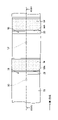
- a diamond layer 10 formed on a base material 20 is prepared.
- the diamond layer 10 has a second main surface 12 on the base material 20 side and a first main surface 11 on the side opposite to the second main surface 12, and includes a color center 930.
- a part of the first main surface 11 is irradiated with the femtosecond laser beam L, and the femtosecond laser beam L is focused on one side of the color center 930 in the first direction parallel to the first main surface 11.
- the portion of the diamond layer 10 focused by the femtosecond laser beam L is altered, and the altered region 933 is formed. With the alteration, the refractive index of the altered region 933 becomes lower than the refractive index of the surroundings.
- the other part of the first main surface 11 is irradiated with the femtosecond laser beam L, and the femtosecond laser beam L is focused on the other side of the color center 930 in the first direction.
- the portion of the diamond layer 10 focused by the femtosecond laser beam L is altered, and the altered region 934 is formed.
- the refractive index of the altered region 934 becomes lower than the refractive index of the surroundings.
- the irradiation of the femtosecond laser beam L is performed, for example, while scanning in a line shape. Therefore, as shown in FIG. 3, the altered regions 933 and 934 are formed in a line shape so as to sandwich the color center 930 between them, for example.
- the refractive index of the region between the altered regions 933 and 934 is higher than the refractive index of the altered regions 933 and 934. Therefore, the altered regions 933 and 934 exert a light confinement effect on the region between the altered regions 933 and 934. That is, an optical waveguide 937 having a core region 936 between the alteration regions 933 and 934 and a light confinement region 935 including the alteration regions 933 and 934 is formed.
- FIG. 2 corresponds to a cross-sectional view taken along line II-II in FIG.
- the optical waveguide 937 formed by this reference example although it is possible to confine light in the first direction, the light confinement effect cannot be obtained in the second direction perpendicular to the first main surface 11.
- FIG. 4 corresponds to a cross-sectional view taken along line IV-IV in FIG.
- the altered regions 931 and 932 have a shape in which the second direction, which is the irradiation direction, is the longitudinal direction in the cross-sectional view from the direction in which the optical waveguide 937 extends, and the dimensions of the altered regions 931 and 932 in the first direction are set. It is difficult to make it large. Therefore, a sufficient light confinement effect cannot be obtained in the second direction.
- the inventor of the present application came up with the following embodiment as a result of diligent studies based on such a reference example.
- the first embodiment relates to a method for manufacturing a quantum circuit.
- 7 to 19 are diagrams showing a method of manufacturing a quantum circuit according to the first embodiment. 7, FIG. 9, FIG. 11, FIG. 13, FIG. 15, FIG. 17 and FIG. 19 are cross-sectional views, and FIGS. 8, 10, 12, 14, 14, 16 and 18 are top views.
- an optical waveguide optically coupled to the color center is formed in the diamond layer including the color center.
- a diamond layer 10 formed on the base material 20 is prepared.
- the base material 20 is composed of, for example, Si or SiO 2 .
- the diamond layer 10 is composed of, for example, a single crystal diamond.
- the diamond layer 10 has a second main surface 12 on the base material 20 side and a first main surface 11 on the side opposite to the second main surface 12, and includes a color center 30.
- the color center 30 is, for example, a nitrogen-vacancy center (NV center) composed of nitrogen and vacancies.
- the color center 30 is composed of a silicon-vacancy center (SiV center) composed of silicon and pores, a germanium-pore center (GeV center) composed of germanium and pores, and tin and pores. Tin-Vacancy Center (SnV Center), Lead-Vacancy Center (PbV Center) composed of lead and vacancies, or Boron-Vacancy Center (BV Center) composed of boron and vacancies May be.
- a groove 38 separated from the color center 30 is formed in the diamond layer 10.
- the groove 38 is formed along the optical waveguide to be formed.
- the groove 38 has, for example, a side surface 38A inclined with respect to the first main surface 11 and a side surface 38B perpendicular to the first main surface 11.
- the side surface 38B is positioned between the color center 30 and the side surface 38A.
- the side surface 38A can be visually recognized from the side of the first main surface 11, and is formed so as to be inclined by, for example, 40 degrees to 50 degrees, preferably 45 degrees with respect to the first main surface 11.
- the side surface 38A is an example of an inclined surface.
- FIG. 9 corresponds to a cross-sectional view taken along the line IX-IX in FIG.
- a reflective film 39 that reflects the femtosecond laser beam is formed on the side surface 38A.
- the reflective film 39 is formed on a part of the side surface 38A.
- the reflective film 39 is formed along the optical waveguide to be formed.
- the reflective film 39 is a film made of a metal such as Au or Al.
- the thickness of the reflective film 39 is not particularly limited, but is, for example, about 0.1 ⁇ m to 1.0 ⁇ m.
- the reflective film 39 can be formed, for example, by a lift-off method.
- FIG. 11 corresponds to a cross-sectional view taken along the line XI-XI in FIG.
- a part of the reflective film 39 is irradiated with the femtosecond laser beam L, and the femtosecond laser beam L reflected by the reflective film 39 is applied to the first main surface of the color center 30. Focus on the 11 side.
- the portion of the diamond layer 10 focused by the femtosecond laser beam L is altered, and the altered region 31 is formed.
- Modifications of the diamond layer 10 include, for example, amorphization, carbonization and ablation. With the alteration, the refractive index of the altered region 31 becomes lower than the refractive index of the surroundings.
- FIG. 13 corresponds to a cross-sectional view taken along line XIII-XIII in FIG.
- the other part of the reflective film 39 is irradiated with the femtosecond laser beam L, and the femtosecond laser beam L reflected by the reflective film 39 is used as the second main component of the color center 30. Focus on the surface 12 side. As a result, the portion of the diamond layer 10 focused by the femtosecond laser beam L is altered, and the altered region 32 is formed. With the alteration, the refractive index of the altered region 32 becomes lower than the refractive index of the surroundings. Irradiation of the femtosecond laser beam L is performed while scanning along the optical waveguide to be formed, and the alteration region 32 is formed along the optical waveguide to be formed.
- the altered region 32 has a shape in which the first direction, which is the irradiation direction, is the longitudinal direction in a cross-sectional view.
- the altered region 32 is an example of the second region.
- FIG. 15 corresponds to a cross-sectional view taken along the line XV-XV in FIG.
- a part of the first main surface 11 is irradiated with the femtosecond laser beam L, and the femtosecond laser beam L is focused on one side of the color center 30 in the first direction. ..
- the portion of the diamond layer 10 focused by the femtosecond laser beam L is altered, and the altered region 33 is formed.
- the refractive index of the altered region 33 becomes lower than the refractive index of the surroundings. Irradiation of the femtosecond laser beam L is performed while scanning along the optical waveguide to be formed, and the alteration region 33 is formed along the optical waveguide to be formed.
- the altered region 33 has a shape in which the second direction, which is the irradiation direction, is the longitudinal direction in a cross-sectional view.
- the altered region 33 is an example of a third region.
- FIG. 17 corresponds to a cross-sectional view taken along line XVII-XVII in FIG.
- the other part of the first main surface 11 is irradiated with the femtosecond laser beam L, and the femtosecond laser beam L is applied to the other side of the color center 30 in the first direction. Condensate.
- the portion of the diamond layer 10 focused by the femtosecond laser beam L is altered, and the altered region 34 is formed.
- the refractive index of the altered region 34 becomes lower than the refractive index of the surroundings. Irradiation of the femtosecond laser beam L is performed while scanning along the optical waveguide to be formed, and the alteration region 34 is formed along the optical waveguide to be formed.
- the altered region 34 has a shape in which the second direction, which is the irradiation direction, is the longitudinal direction in a cross-sectional view.
- the altered region 34 is an example of the fourth region.
- FIG. 19 corresponds to a cross-sectional view taken along the XIX-XIX line in FIG.
- An example of the irradiation conditions of the femtosecond laser beam L when forming the altered regions 31 to 34 is as follows. That is, the wavelength is 800 nm, the pulse width is 50 fs to 100 fs, the pulse energy is 50 nJ to 1000 nJ, and the repetition frequency is 250 kHz to 500 kHz.
- the altered regions 31 to 34 are formed in a line shape so as to surround the color center 30 in a cross-sectional view, for example.
- the refractive index of the region surrounded by the altered regions 31 to 34 is higher than the refractive index of the altered regions 31 to 34. Therefore, the altered regions 31 to 34 exert a light confinement effect on the region surrounded by the altered regions 31 to 34. That is, an optical waveguide 37 having a core region 36 surrounded by alteration regions 31 to 34 and a light confinement region 35 having alteration regions 31 to 34 is formed.
- the quantum circuit 1 provided with the optical waveguide 37 optically coupled to the color center 30 can be manufactured.
- the order of formation of the altered regions 31 to 34 is not particularly limited.
- the alteration regions 31 and 32 may be formed after the alteration regions 33 and 34 are formed.
- the altered regions 31 and 32 have a shape in which the first direction is the longitudinal direction in the cross-sectional view
- the altered regions 33 and 34 have a shape in which the second direction is the longitudinal direction in the cross-sectional view. That is, the dimensions of the altered regions 31 and 32 in the first direction are larger than the dimensions of the second direction, and the dimensions of the altered regions 33 and 34 in the second direction are larger than the dimensions of the first direction. Therefore, the alteration regions 31 and 32 can confine the light in the core region 36 in the second direction, and the alteration regions 33 and 34 can confine the light in the core region 36 in the first direction. Therefore, the light emitted from the color center 30 can be efficiently coupled to the optical waveguide 37, and the loss of the optical signal propagating through the optical waveguide 37 can be reduced.
- the reflective film 39 is formed at a desired position from the first direction via the reflective film 39.
- the femtosecond laser beam L can be focused.
- the color center 30 may be intentionally formed.
- 20 to 21 are diagrams showing a method of forming the color center 30. 20 and 21 are cross-sectional views. As shown in FIG. 20, the pore 30X is formed by condensing a single femtosecond laser beam L on the diamond layer 10. Next, annealing is performed in a nitrogen atmosphere, and as shown in FIG. 21, an NV center in which a pore 30X and a nitrogen atom are paired is formed as a color center 30.
- An example of annealing conditions is as follows. That is, the temperature is 1000 ° C. and the time is 3 hours.
- the second embodiment differs from the first embodiment mainly in the arrangement of the reflective film.
- 22 to 24 are diagrams showing a method of manufacturing a quantum circuit according to a second embodiment. 22 is a top view, and FIGS. 23 and 24 are cross-sectional views.
- the process up to the formation of the groove 38 is performed in the same manner as in the first embodiment (see FIGS. 8 and 9).
- the reflective film 39 is placed on the side surface 38A, on the surface of the base material 20 exposed to the bottom of the groove 38, and on the first main surface 11 connected to the side surface 38A. To form.
- the altered regions 31 to 34 are formed in the same manner as in the first embodiment.
- the quantum circuit 2 provided with the optical waveguide 37 optically coupled to the color center 30 can be manufactured.
- the reflective film 39 is also formed on the surface of the base material 20 exposed to the bottom of the groove 38 and on the first main surface 11 connected to the side surface 38A, it is formed in the thickness direction of the diamond layer 10. The range in which the alteration regions 31 and 32 can be formed can be expanded.
- the third embodiment differs from the first embodiment mainly in the number of color centers and optical waveguides.
- 25 to 30 are diagrams showing a method of manufacturing a quantum circuit according to a third embodiment.
- 25, 27, 29 and 30 are cross-sectional views, and 26 and 28 are top views.
- two optical waveguides individually optical-coupled to the color centers are formed in the diamond layer containing the two color centers.
- the diamond layer 10 including the color centers 30 and 40 formed on the base material 20 and formed apart in the first direction is prepared.
- the color center 40 is, for example, an NV center, a SiV center, a GeV center, a SnV center, a PbV center, or a BV center, similarly to the color center 30.
- a groove 38 away from the color center 30 and a groove 48 away from the color center 40 are formed in the diamond layer 10.
- the grooves 38 and 48 are formed along the optical waveguide to be formed.
- the grooves 38 and 48 are formed between the color center 30 and the color center 40 in the first direction
- the groove 38 is formed on the color center 30 side of the groove 48
- the groove 48 is formed on the color center 30 side of the groove 38. It is formed on the 40 side.
- the groove 48 has, for example, a side surface 48A inclined with respect to the first main surface 11 and a side surface 48B perpendicular to the first main surface 11.
- the side surface 48B is positioned between the color center 40 and the side surface 48A.
- the side surface 48A can be visually recognized from the first main surface 11 side, and is formed so as to be inclined by, for example, 40 degrees to 50 degrees, preferably 45 degrees with respect to the first main surface 11.
- the side surface 48A is an example of an inclined surface.
- FIG. 27 corresponds to a cross-sectional view taken along the line XXVII-XXVII in FIG.
- the reflective film 49 that reflects the femtosecond laser beam on the side surface 38A, the side surface 48A, and the first main surface 11 connected to the side surface 38A and the side surface 48A.
- the reflective film 49 is formed along the optical waveguide to be formed.
- the reflective film 49 is a film made of a metal such as Au or Al.
- the thickness of the reflective film 49 is not particularly limited, but is, for example, about 0.1 ⁇ m to 1.0 ⁇ m.
- the reflective film 49 can be formed by, for example, a lift-off method.
- FIG. 29 corresponds to a cross-sectional view taken along the line XXIX-XXIX in FIG. 28.
- the altered regions 31 to 34 are formed in the same manner as in the first embodiment. Further, the altered regions 41 to 44 are formed in the same manner as the formation of the altered regions 31 to 34, respectively.
- the altered regions 41 to 44 are formed in a line shape, for example, so as to surround the color center 40 in a cross-sectional view.
- the refractive index of the region surrounded by the altered regions 41 to 44 is higher than the refractive index of the altered regions 41 to 44. Therefore, the altered regions 41 to 44 exert a light confinement effect on the region surrounded by the altered regions 41 to 44. That is, an optical waveguide 47 having a core region 46 surrounded by alteration regions 41 to 44 and a light confinement region 45 including alteration regions 41 to 44 is formed.
- the quantum circuit 3 including the optical waveguide 37 optically coupled to the color center 30 and the optical waveguide 47 optically coupled to the color center 40 can be manufactured.
- the order of formation of the altered regions 31 to 34 and 41 to 44 is not particularly limited.
- the same effect as that of the first embodiment can be obtained by the third embodiment.
- the loss of the optical signal propagating through the optical waveguide 47 can be reduced. Further, it is easy to increase the number of qubits included in the quantum circuit 3.
- the groove 38 and the groove 48 can be formed at the same time.
- the reflective film may be individually formed on the side surfaces 38A and 48A, and even in this case, the reflective film can be formed on the side surface 38A and the side surface 48A at the same time.
- the fourth embodiment differs from the third embodiment mainly in the arrangement of the groove and the reflective film.
- 31 to 36 are diagrams showing a method of manufacturing a quantum circuit according to a fourth embodiment.
- 31, FIG. 33, FIG. 35 and FIG. 36 are cross-sectional views, and FIGS. 32 and 34 are top views.
- two optical waveguides individually optical-coupled to the color center are formed in the diamond layer including the two color centers.
- a diamond layer 10 including color centers 30 and 50 formed on the base material 20 and formed apart in the first direction is prepared. Similar to the color center 30, the color center 50 is, for example, an NV center, a SiV center, a GeV center, a SnV center, a PbV center, or a BV center.
- a groove 38 away from the color center 30 and a groove 58 away from the color center 50 are formed in the diamond layer 10.
- the grooves 38 and 58 are formed along the optical waveguide to be formed.
- the groove 38 is formed between the color center 30 and the color center 50 in the first direction, and the groove 58 is formed so as to be farther from the groove 38 than the color center 50.
- the groove 58 has, for example, a side surface 58A inclined with respect to the first main surface 11 and a side surface 58B perpendicular to the first main surface 11.
- the side surface 58B is positioned between the color center 50 and the side surface 58A.
- the side surface 58A can be visually recognized from the side of the first main surface 11, and is formed so as to be inclined by, for example, 40 degrees to 50 degrees, preferably 45 degrees with respect to the first main surface 11.
- the side surface 58A is an example of an inclined surface.
- FIG. 33 corresponds to a cross-sectional view taken along the line XXXIII-XXXIII in FIG.
- a reflective film 39 that reflects the femtosecond laser beam is formed on the side surface 38A, and a reflective film 59 that reflects the femtosecond laser beam is formed on the side surface 58A.
- the reflective film 39 is formed on a part of the side surface 38A, and the reflective film 59 is formed on a part of the side surface 58A.
- the reflective films 39 and 59 are formed along the optical waveguide to be formed.
- the reflective film 59 is a film made of a metal such as Au or Al.
- the thickness of the reflective film 59 is not particularly limited, but is, for example, about 0.1 ⁇ m to 1.0 ⁇ m.
- the reflective film 59 can be formed, for example, by a lift-off method.
- the reflective films 39 and 59 can be formed at the same time.
- FIG. 35 corresponds to a cross-sectional view taken along the line XXXV-XXXV in FIG.
- the altered regions 31 to 34 are formed in the same manner as in the first embodiment.
- the altered regions 51 to 54 are formed in the same manner as the formation of the altered regions 31 to 34, respectively.
- the altered regions 51 to 54 are formed in a line shape, for example, so as to surround the color center 50 in a cross-sectional view.
- the refractive index of the region surrounded by the altered regions 51 to 54 is higher than the refractive index of the altered regions 51 to 54. Therefore, the altered regions 51 to 54 exert a light confinement effect on the region surrounded by the altered regions 51 to 54. That is, an optical waveguide 57 having a core region 56 surrounded by alteration regions 51 to 54 and a light confinement region 55 including alteration regions 51 to 54 is formed.
- the quantum circuit 4 including the optical waveguide 37 optically coupled to the color center 30 and the optical waveguide 57 optically coupled to the color center 50 can be manufactured.
- the order of formation of the altered regions 31 to 34 and 51 to 54 is not particularly limited.
- the fourth embodiment The same effect as that of the first embodiment can be obtained by the fourth embodiment.
- the loss of the optical signal propagating through the optical waveguide 57 can be reduced. Further, it is easy to increase the number of qubits included in the quantum circuit 4.
- the groove 38 and the groove 58 can be formed at the same time, and the reflective film 39 and the reflective film 59 can be formed at the same time.
- the fifth embodiment differs from the first embodiment mainly in the number of color centers and optical waveguides.
- 37 to 40 are diagrams showing a method of manufacturing a quantum circuit according to a fifth embodiment.
- 37 to 40 are cross-sectional views. It is a figure which shows the manufacturing method of the quantum circuit which concerns on 5th Embodiment.
- four optical waveguides individually optical-coupled to the color centers are formed in the diamond layer containing the four color centers.
- a diamond layer 10 including color centers 30, 60, 70 and 80 formed on the substrate 20 and formed apart in the first direction is prepared.
- the color centers 60, 70 and 80 are, for example, NV centers, SiV centers, GeV centers, SnV centers, PbV centers or BV centers.
- the color center 30 and the color center 60 are located close to each other in the first direction, and the color center 70 and the color center 80 are located close to each other.
- a groove 68 away from the color centers 30 and 60 and a groove 78 away from the color centers 70 and 80 are formed in the diamond layer 10.
- the grooves 68 and 78 are formed along the optical waveguide to be formed.
- the groove 68 is formed between the color centers 30 and 60 and the color centers 70 and 80 in the first direction
- the groove 78 is formed so as to be farther from the groove 68 than the color centers 70 and 80.
- the groove 68 has, for example, a side surface 68A inclined with respect to the first main surface 11 and a side surface 68B perpendicular to the first main surface 11.
- the side surface 68B is located between the color centers 30 and 60 and the side surface 68A.
- the side surface 68A can be visually recognized from the first main surface 11 side, and is formed so as to be inclined by, for example, 40 degrees to 50 degrees, preferably 45 degrees with respect to the first main surface 11.
- the groove 78 has, for example, a side surface 78A inclined with respect to the first main surface 11 and a side surface 78B perpendicular to the first main surface 11.
- the side surface 78B is located between the color centers 70 and 80 and the side surface 78A.
- the side surface 78A can be visually recognized from the side of the first main surface 11, and is formed so as to be inclined by, for example, 40 to 50 degrees, preferably 45 degrees with respect to the first main surface 11.
- the sides 68A and 78A are examples of inclined surfaces.
- a reflective film 69 that reflects the femtosecond laser beam is formed on the side surface 68A, and a reflective film 79 that reflects the femtosecond laser beam is formed on the side surface 78A.
- the reflective film 69 is formed on a part of the side surface 68A
- the reflective film 79 is formed on a part of the side surface 78A.
- the reflective films 69 and 79 are formed along the optical waveguide to be formed.
- the reflective films 69 and 79 are films made of a metal such as Au or Al.
- the thicknesses of the reflective films 69 and 79 are not particularly limited, but are, for example, about 0.1 ⁇ m to 1.0 ⁇ m.
- the reflective films 69 and 79 can be formed, for example, by the lift-off method. Reflective films 69 and 79 can be formed at the same time.
- the altered regions 31 to 34 are formed in the same manner as in the first embodiment. Further, the altered regions 61 to 64, the altered regions 71 to 74, and the altered regions 81 to 84 are formed in the same manner as in the formation of the altered regions 31 to 34, respectively.
- the altered regions 61 to 64 are formed in a line shape, for example, so as to surround the color center 60 in a cross-sectional view.
- the altered regions 71 to 74 are formed in a line shape, for example, so as to surround the color center 70 in a cross-sectional view.
- the altered regions 81 to 84 are formed in a line shape, for example, so as to surround the color center 80 in a cross-sectional view.
- the refractive index of the region surrounded by the altered regions 61 to 64 is higher than the refractive index of the altered regions 61 to 64. Therefore, the altered regions 61 to 64 exert a light confinement effect on the regions surrounded by the altered regions 61 to 64. That is, an optical waveguide 67 having a core region 66 surrounded by alteration regions 61 to 64 and a light confinement region 65 including alteration regions 61 to 64 is formed.
- the refractive index of the region surrounded by the altered regions 71 to 74 is higher than the refractive index of the altered regions 71 to 74. Therefore, the altered regions 71 to 74 exert a light confinement effect on the region surrounded by the altered regions 71 to 74. That is, an optical waveguide 77 having a core region 76 surrounded by alteration regions 71 to 74 and a light confinement region 75 including alteration regions 71 to 74 is formed.
- the refractive index of the region surrounded by the altered regions 81 to 84 is higher than the refractive index of the altered regions 81 to 84. Therefore, the altered regions 81 to 84 exert a light confinement effect on the regions surrounded by the altered regions 81 to 84. That is, an optical waveguide 87 having a core region 86 surrounded by alteration regions 81 to 84 and a light confinement region 85 including alteration regions 81 to 84 is formed.
- the optical waveguide 37 optically coupled to the color center 30, the optical waveguide 67 optically coupled to the color center 60, the optical waveguide 77 optically coupled to the color center 70, and the optical waveguide 80 optically coupled to the color center 80. It is possible to manufacture a quantum circuit 5 provided with an optical waveguide 87 to be formed.
- the order of formation of the altered regions 61 to 64, 71 to 74 and 81 to 84 is not particularly limited.
- the same effect as that of the first embodiment can be obtained by the fifth embodiment. Further, the loss of the optical signal propagating through the optical waveguides 67, 77, 87 can also be reduced. Further, it is easy to increase the number of qubits included in the quantum circuit 5.
- the color centers 40, 50, 60, 70 and 80 may be formed at desired positions by the methods shown in FIGS. 20 to 21.
- the reflective film can be used as a marker to align the photodetector coupled to the optical waveguide.
- the reflective film can be used as a marker to align the photodetector coupled to the optical waveguide.
- the number of color centers and optical waveguides included in the quantum circuit of the present disclosure is not limited.
- the quantum circuits 1, 2, 3, 4, and 5 according to these embodiments can be used as a quantum circuit 101, for example, by being incorporated in the quantum computer 100.
- Quantum circuit 10 Diamond layer 11: First main surface 12: Second main surface 20: Base material 30, 40, 50, 60, 70, 80: Color centers 31 to 34, 41-44, 51-54, 61-64, 71-74, 81-84: Altered region 35, 45, 55, 65, 75, 85: Optical confinement region 36, 46, 56, 66, 76, 86: Core Region 37, 47, 57, 67, 77, 87: Optical Waveguide 38, 48, 58, 68, 78: Groove 38A, 48A, 58A, 68A, 78A: Side 39, 49, 59, 69, 79: Reflective film 100 : Quantum computer
Landscapes
- Physics & Mathematics (AREA)
- Engineering & Computer Science (AREA)
- Microelectronics & Electronic Packaging (AREA)
- General Physics & Mathematics (AREA)
- Optics & Photonics (AREA)
- Optical Integrated Circuits (AREA)
Priority Applications (5)
| Application Number | Priority Date | Filing Date | Title |
|---|---|---|---|
| PCT/JP2020/044622 WO2022118366A1 (ja) | 2020-12-01 | 2020-12-01 | 量子回路、量子コンピュータ及び量子回路の製造方法 |
| JP2022566521A JP7540506B2 (ja) | 2020-12-01 | 2020-12-01 | 量子回路の製造方法 |
| CN202080105873.2A CN116235091A (zh) | 2020-12-01 | 2020-12-01 | 量子电路、量子计算机和量子电路的制造方法 |
| EP20964220.6A EP4258029A4 (en) | 2020-12-01 | 2020-12-01 | QUANTUM CIRCUIT, QUANTUM COMPUTER AND METHOD FOR PRODUCING QUANTUM CIRCUIT |
| US18/189,729 US12461305B2 (en) | 2020-12-01 | 2023-03-24 | Quantum circuit, quantum computer, and method of manufacturing quantum circuit |
Applications Claiming Priority (1)
| Application Number | Priority Date | Filing Date | Title |
|---|---|---|---|
| PCT/JP2020/044622 WO2022118366A1 (ja) | 2020-12-01 | 2020-12-01 | 量子回路、量子コンピュータ及び量子回路の製造方法 |
Related Child Applications (1)
| Application Number | Title | Priority Date | Filing Date |
|---|---|---|---|
| US18/189,729 Continuation US12461305B2 (en) | 2020-12-01 | 2023-03-24 | Quantum circuit, quantum computer, and method of manufacturing quantum circuit |
Publications (1)
| Publication Number | Publication Date |
|---|---|
| WO2022118366A1 true WO2022118366A1 (ja) | 2022-06-09 |
Family
ID=81852995
Family Applications (1)
| Application Number | Title | Priority Date | Filing Date |
|---|---|---|---|
| PCT/JP2020/044622 Ceased WO2022118366A1 (ja) | 2020-12-01 | 2020-12-01 | 量子回路、量子コンピュータ及び量子回路の製造方法 |
Country Status (5)
| Country | Link |
|---|---|
| US (1) | US12461305B2 (https=) |
| EP (1) | EP4258029A4 (https=) |
| JP (1) | JP7540506B2 (https=) |
| CN (1) | CN116235091A (https=) |
| WO (1) | WO2022118366A1 (https=) |
Cited By (1)
| Publication number | Priority date | Publication date | Assignee | Title |
|---|---|---|---|---|
| WO2024042602A1 (ja) * | 2022-08-23 | 2024-02-29 | 富士通株式会社 | 量子デバイス及び量子デバイスの製造方法 |
Families Citing this family (1)
| Publication number | Priority date | Publication date | Assignee | Title |
|---|---|---|---|---|
| CN120469014B (zh) * | 2025-04-27 | 2026-03-24 | 武汉大学 | 光电共封装器件及其制备方法 |
Citations (4)
| Publication number | Priority date | Publication date | Assignee | Title |
|---|---|---|---|---|
| JP2003506731A (ja) * | 1999-07-29 | 2003-02-18 | コーニング インコーポレイテッド | フェムト秒パルスレーザを用いるシリカベースガラスへの光デバイスの直接書込 |
| JP2005538392A (ja) * | 2002-08-02 | 2005-12-15 | フェムトニックス・コーポレーション | フェムト秒光パルスを有する光導波路デバイスのミクロ構造化 |
| JP2013544441A (ja) | 2010-12-03 | 2013-12-12 | アデレイド リサーチ アンド イノヴェイション プロプライエタリー リミテッド | 光の増幅のための素子及びその製造方法 |
| US9157859B2 (en) | 2011-06-13 | 2015-10-13 | President And Fellows Of Harvard College | Efficient fluorescence detection in solid state spin systems |
Family Cites Families (4)
| Publication number | Priority date | Publication date | Assignee | Title |
|---|---|---|---|---|
| JP2013076618A (ja) * | 2011-09-30 | 2013-04-25 | Sony Corp | 光伝導素子、レンズ、テラヘルツ放射顕微鏡及びデバイスの製造方法 |
| CN103743390B (zh) * | 2013-12-31 | 2016-08-17 | 北京航空航天大学 | 基于nv-色心金刚石—mems混合结构的陀螺仪及制作方法 |
| RU2655026C1 (ru) * | 2017-04-24 | 2018-05-23 | Федеральное государственное бюджетное научное учреждение "Федеральный исследовательский центр Институт прикладной физики Российской академии наук" (ИПФ РАН) | Способ получения фотолюминесценции отдельных центров окраски в осажденном из газовой фазы алмазе |
| WO2021222097A1 (en) * | 2020-04-28 | 2021-11-04 | Board Of Trustees Of Michigan State University | Laser activated luminescence system |
-
2020
- 2020-12-01 EP EP20964220.6A patent/EP4258029A4/en active Pending
- 2020-12-01 JP JP2022566521A patent/JP7540506B2/ja active Active
- 2020-12-01 CN CN202080105873.2A patent/CN116235091A/zh active Pending
- 2020-12-01 WO PCT/JP2020/044622 patent/WO2022118366A1/ja not_active Ceased
-
2023
- 2023-03-24 US US18/189,729 patent/US12461305B2/en active Active
Patent Citations (5)
| Publication number | Priority date | Publication date | Assignee | Title |
|---|---|---|---|---|
| JP2003506731A (ja) * | 1999-07-29 | 2003-02-18 | コーニング インコーポレイテッド | フェムト秒パルスレーザを用いるシリカベースガラスへの光デバイスの直接書込 |
| JP2005538392A (ja) * | 2002-08-02 | 2005-12-15 | フェムトニックス・コーポレーション | フェムト秒光パルスを有する光導波路デバイスのミクロ構造化 |
| JP2013544441A (ja) | 2010-12-03 | 2013-12-12 | アデレイド リサーチ アンド イノヴェイション プロプライエタリー リミテッド | 光の増幅のための素子及びその製造方法 |
| US8837534B2 (en) | 2010-12-03 | 2014-09-16 | Adelaide Research & Innovation Pty Ltd. | Element for the amplification of a light and method of making the same |
| US9157859B2 (en) | 2011-06-13 | 2015-10-13 | President And Fellows Of Harvard College | Efficient fluorescence detection in solid state spin systems |
Non-Patent Citations (7)
| Title |
|---|
| "Diamond photonics platform enabled by femtosecond laser writing", SCIENTIFIC REPORTS, vol. 6, 2016, pages 35566 |
| "Integrated waveguides and deterministically positioned nitrogen vacancy centers in diamond created by femtosecond laser writing", OPTICS LETTERS, vol. 43, no. 15, 2018, pages 3586 - 3589 |
| BOOTH MARTIN J; SALTER PATRICK S: "Dynamic optical laser fabrication for engineering of quantum photonic devices", QUANTUM SENSING AND NANO ELECTRONICS AND PHOTONICS XVI, vol. 10926, 1 February 2019 (2019-02-01), pages 10926Y - 1-10926Y-6, XP060119528 * |
| HADDEN J. P., BHARADWAJ V., SOTILLO B., RAMPINI S., OSELLAME R., WITMER J. D., JAYAKUMAR H., FERNANDEZ T. T., CHIAPPINI A., ARMELL: "Integrated waveguides and deterministically positioned nitrogen vacancy centers in diamond created by femtosecond laser writing", OPTICS LETTERS, vol. 43, no. 15, 1 August 2018 (2018-08-01), pages 3586 - 3589, XP081149571 * |
| HANAFI HAISSAM, KROESEN SEBASTIAN, LEWES-MALANDRAKIS GEORGIA, NEBEL CHRISTOPH, PERNICE WOLFRAM H. P., DENZ CORNELIA: "Polycrystalline diamond photonic waveguides realized by femtosecond laser lithography", OPTICAL MATERIALS EXPRESS, vol. 9, no. 7, 24 June 2019 (2019-06-24), pages 3109 - 3114, XP055942211 * |
| See also references of EP4258029A4 |
| SOTILLO BELÉN, BHARADWAJ VIBHAV, HADDEN J. P., SAKAKURA MASAAKI, CHIAPPINI ANDREA, FERNANDEZ TONEY TEDDY, LONGHI STEFANO, JEDRKIEW: "Diamond photonics platform enabled by femtosecond laser writing", SCIENTIFIC REPORTS, vol. 6, no. 35566, 17 October 2016 (2016-10-17), pages 1 - 9, XP055942206 * |
Cited By (1)
| Publication number | Priority date | Publication date | Assignee | Title |
|---|---|---|---|---|
| WO2024042602A1 (ja) * | 2022-08-23 | 2024-02-29 | 富士通株式会社 | 量子デバイス及び量子デバイスの製造方法 |
Also Published As
| Publication number | Publication date |
|---|---|
| EP4258029A1 (en) | 2023-10-11 |
| US12461305B2 (en) | 2025-11-04 |
| CN116235091A (zh) | 2023-06-06 |
| EP4258029A4 (en) | 2024-01-17 |
| JP7540506B2 (ja) | 2024-08-27 |
| US20230280528A1 (en) | 2023-09-07 |
| JPWO2022118366A1 (https=) | 2022-06-09 |
Similar Documents
| Publication | Publication Date | Title |
|---|---|---|
| US6393180B1 (en) | Providing a refractive index change in an ion diffused material | |
| EP1522882A1 (en) | Optical waveguide having mirror surface formed by laser beam machining | |
| JP2019532004A (ja) | 非軸対称ビームスポットを用いて透明被加工物をレーザ加工するための装置及び方法 | |
| US20060213880A1 (en) | Laser surface treatment | |
| US12461305B2 (en) | Quantum circuit, quantum computer, and method of manufacturing quantum circuit | |
| JPH10128563A (ja) | マイクロレンズに対するレーザ加工方法 | |
| US20080264910A1 (en) | Process for Fabricating Optical Waveguides | |
| CN111902754A (zh) | 组件、光学连接器和将光纤结合到基板的方法 | |
| EP3164745B1 (en) | High power visible laser with a laser-fabricated nonlinear waveguide | |
| US6897433B2 (en) | Method for rewriting data in three-dimensional optical memory device fabricated in glass by ultra-short light pulse | |
| JP3917033B2 (ja) | 光通信用ファイバアレイおよびその製造方法 | |
| WO2021009961A1 (ja) | 複合材の分断方法 | |
| US20120268939A1 (en) | Method of laser processing | |
| JP3917034B2 (ja) | 光コネクタおよびその製造方法 | |
| CN209327609U (zh) | 一种多层光纤以及实现双激光输出的激光器系统 | |
| JP3925209B2 (ja) | 導波路の製造方法 | |
| JP7561089B2 (ja) | 複合材の分断方法 | |
| JPWO2022118366A5 (https=) | ||
| Bado et al. | Dramatic improvements in waveguide manufacturing with femtosecond lasers | |
| JP3921987B2 (ja) | フォトニック結晶導波路及びその製造方法 | |
| CN114502520B (zh) | Yag陶瓷接合体及其制造方法 | |
| JP2007108261A (ja) | 偏波保持光導波路およびその製造方法 | |
| Arai et al. | Fiber chirped pulse amplification system for micromachining | |
| JP2005241813A (ja) | 光路変換光導波路とその製造方法 | |
| JPWO2021157135A5 (https=) |
Legal Events
| Date | Code | Title | Description |
|---|---|---|---|
| 121 | Ep: the epo has been informed by wipo that ep was designated in this application |
Ref document number: 20964220 Country of ref document: EP Kind code of ref document: A1 |
|
| ENP | Entry into the national phase |
Ref document number: 2022566521 Country of ref document: JP Kind code of ref document: A |
|
| NENP | Non-entry into the national phase |
Ref country code: DE |
|
| ENP | Entry into the national phase |
Ref document number: 2020964220 Country of ref document: EP Effective date: 20230703 |