WO2022113733A1 - 受光素子、測距システム、および、電子機器 - Google Patents
受光素子、測距システム、および、電子機器 Download PDFInfo
- Publication number
- WO2022113733A1 WO2022113733A1 PCT/JP2021/041270 JP2021041270W WO2022113733A1 WO 2022113733 A1 WO2022113733 A1 WO 2022113733A1 JP 2021041270 W JP2021041270 W JP 2021041270W WO 2022113733 A1 WO2022113733 A1 WO 2022113733A1
- Authority
- WO
- WIPO (PCT)
- Prior art keywords
- semiconductor region
- pixel
- region
- concentration
- light receiving
- Prior art date
- Legal status (The legal status is an assumption and is not a legal conclusion. Google has not performed a legal analysis and makes no representation as to the accuracy of the status listed.)
- Ceased
Links
Images









Classifications
-
- H—ELECTRICITY
- H10—SEMICONDUCTOR DEVICES; ELECTRIC SOLID-STATE DEVICES NOT OTHERWISE PROVIDED FOR
- H10F—INORGANIC SEMICONDUCTOR DEVICES SENSITIVE TO INFRARED RADIATION, LIGHT, ELECTROMAGNETIC RADIATION OF SHORTER WAVELENGTH OR CORPUSCULAR RADIATION
- H10F77/00—Constructional details of devices covered by this subclass
- H10F77/10—Semiconductor bodies
- H10F77/14—Shape of semiconductor bodies; Shapes, relative sizes or dispositions of semiconductor regions within semiconductor bodies
- H10F77/147—Shapes of bodies
-
- G—PHYSICS
- G01—MEASURING; TESTING
- G01C—MEASURING DISTANCES, LEVELS OR BEARINGS; SURVEYING; NAVIGATION; GYROSCOPIC INSTRUMENTS; PHOTOGRAMMETRY OR VIDEOGRAMMETRY
- G01C3/00—Measuring distances in line of sight; Optical rangefinders
- G01C3/02—Details
- G01C3/06—Use of electric means to obtain final indication
-
- G—PHYSICS
- G01—MEASURING; TESTING
- G01S—RADIO DIRECTION-FINDING; RADIO NAVIGATION; DETERMINING DISTANCE OR VELOCITY BY USE OF RADIO WAVES; LOCATING OR PRESENCE-DETECTING BY USE OF THE REFLECTION OR RERADIATION OF RADIO WAVES; ANALOGOUS ARRANGEMENTS USING OTHER WAVES
- G01S17/00—Systems using the reflection or reradiation of electromagnetic waves other than radio waves, e.g. lidar systems
- G01S17/02—Systems using the reflection of electromagnetic waves other than radio waves
- G01S17/06—Systems determining position data of a target
- G01S17/08—Systems determining position data of a target for measuring distance only
-
- G—PHYSICS
- G01—MEASURING; TESTING
- G01S—RADIO DIRECTION-FINDING; RADIO NAVIGATION; DETERMINING DISTANCE OR VELOCITY BY USE OF RADIO WAVES; LOCATING OR PRESENCE-DETECTING BY USE OF THE REFLECTION OR RERADIATION OF RADIO WAVES; ANALOGOUS ARRANGEMENTS USING OTHER WAVES
- G01S17/00—Systems using the reflection or reradiation of electromagnetic waves other than radio waves, e.g. lidar systems
- G01S17/88—Lidar systems specially adapted for specific applications
- G01S17/89—Lidar systems specially adapted for specific applications for mapping or imaging
- G01S17/894—Three-dimensional [3D] imaging with simultaneous measurement of time-of-flight at a two-dimensional [2D] array of receiver pixels, e.g. time-of-flight cameras or flash lidar
-
- G—PHYSICS
- G01—MEASURING; TESTING
- G01S—RADIO DIRECTION-FINDING; RADIO NAVIGATION; DETERMINING DISTANCE OR VELOCITY BY USE OF RADIO WAVES; LOCATING OR PRESENCE-DETECTING BY USE OF THE REFLECTION OR RERADIATION OF RADIO WAVES; ANALOGOUS ARRANGEMENTS USING OTHER WAVES
- G01S17/00—Systems using the reflection or reradiation of electromagnetic waves other than radio waves, e.g. lidar systems
- G01S17/88—Lidar systems specially adapted for specific applications
- G01S17/93—Lidar systems specially adapted for specific applications for anti-collision purposes
- G01S17/931—Lidar systems specially adapted for specific applications for anti-collision purposes of land vehicles
-
- H—ELECTRICITY
- H10—SEMICONDUCTOR DEVICES; ELECTRIC SOLID-STATE DEVICES NOT OTHERWISE PROVIDED FOR
- H10F—INORGANIC SEMICONDUCTOR DEVICES SENSITIVE TO INFRARED RADIATION, LIGHT, ELECTROMAGNETIC RADIATION OF SHORTER WAVELENGTH OR CORPUSCULAR RADIATION
- H10F30/00—Individual radiation-sensitive semiconductor devices in which radiation controls the flow of current through the devices, e.g. photodetectors
- H10F30/20—Individual radiation-sensitive semiconductor devices in which radiation controls the flow of current through the devices, e.g. photodetectors the devices having potential barriers, e.g. phototransistors
- H10F30/21—Individual radiation-sensitive semiconductor devices in which radiation controls the flow of current through the devices, e.g. photodetectors the devices having potential barriers, e.g. phototransistors the devices being sensitive to infrared, visible or ultraviolet radiation
- H10F30/22—Individual radiation-sensitive semiconductor devices in which radiation controls the flow of current through the devices, e.g. photodetectors the devices having potential barriers, e.g. phototransistors the devices being sensitive to infrared, visible or ultraviolet radiation the devices having only one potential barrier, e.g. photodiodes
- H10F30/225—Individual radiation-sensitive semiconductor devices in which radiation controls the flow of current through the devices, e.g. photodetectors the devices having potential barriers, e.g. phototransistors the devices being sensitive to infrared, visible or ultraviolet radiation the devices having only one potential barrier, e.g. photodiodes the potential barrier working in avalanche mode, e.g. avalanche photodiodes
-
- H—ELECTRICITY
- H10—SEMICONDUCTOR DEVICES; ELECTRIC SOLID-STATE DEVICES NOT OTHERWISE PROVIDED FOR
- H10F—INORGANIC SEMICONDUCTOR DEVICES SENSITIVE TO INFRARED RADIATION, LIGHT, ELECTROMAGNETIC RADIATION OF SHORTER WAVELENGTH OR CORPUSCULAR RADIATION
- H10F39/00—Integrated devices, or assemblies of multiple devices, comprising at least one element covered by group H10F30/00, e.g. radiation detectors comprising photodiode arrays
- H10F39/80—Constructional details of image sensors
- H10F39/802—Geometry or disposition of elements in pixels, e.g. address-lines or gate electrodes
- H10F39/8027—Geometry of the photosensitive area
-
- H—ELECTRICITY
- H10—SEMICONDUCTOR DEVICES; ELECTRIC SOLID-STATE DEVICES NOT OTHERWISE PROVIDED FOR
- H10F—INORGANIC SEMICONDUCTOR DEVICES SENSITIVE TO INFRARED RADIATION, LIGHT, ELECTROMAGNETIC RADIATION OF SHORTER WAVELENGTH OR CORPUSCULAR RADIATION
- H10F39/00—Integrated devices, or assemblies of multiple devices, comprising at least one element covered by group H10F30/00, e.g. radiation detectors comprising photodiode arrays
- H10F39/80—Constructional details of image sensors
- H10F39/803—Pixels having integrated switching, control, storage or amplification elements
- H10F39/8033—Photosensitive area
-
- H—ELECTRICITY
- H10—SEMICONDUCTOR DEVICES; ELECTRIC SOLID-STATE DEVICES NOT OTHERWISE PROVIDED FOR
- H10F—INORGANIC SEMICONDUCTOR DEVICES SENSITIVE TO INFRARED RADIATION, LIGHT, ELECTROMAGNETIC RADIATION OF SHORTER WAVELENGTH OR CORPUSCULAR RADIATION
- H10F39/00—Integrated devices, or assemblies of multiple devices, comprising at least one element covered by group H10F30/00, e.g. radiation detectors comprising photodiode arrays
- H10F39/80—Constructional details of image sensors
- H10F39/807—Pixel isolation structures
-
- H—ELECTRICITY
- H10—SEMICONDUCTOR DEVICES; ELECTRIC SOLID-STATE DEVICES NOT OTHERWISE PROVIDED FOR
- H10F—INORGANIC SEMICONDUCTOR DEVICES SENSITIVE TO INFRARED RADIATION, LIGHT, ELECTROMAGNETIC RADIATION OF SHORTER WAVELENGTH OR CORPUSCULAR RADIATION
- H10F77/00—Constructional details of devices covered by this subclass
- H10F77/10—Semiconductor bodies
- H10F77/14—Shape of semiconductor bodies; Shapes, relative sizes or dispositions of semiconductor regions within semiconductor bodies
-
- H—ELECTRICITY
- H10—SEMICONDUCTOR DEVICES; ELECTRIC SOLID-STATE DEVICES NOT OTHERWISE PROVIDED FOR
- H10F—INORGANIC SEMICONDUCTOR DEVICES SENSITIVE TO INFRARED RADIATION, LIGHT, ELECTROMAGNETIC RADIATION OF SHORTER WAVELENGTH OR CORPUSCULAR RADIATION
- H10F77/00—Constructional details of devices covered by this subclass
- H10F77/95—Circuit arrangements
- H10F77/953—Circuit arrangements for devices having potential barriers
- H10F77/959—Circuit arrangements for devices having potential barriers for devices working in avalanche mode
-
- G—PHYSICS
- G01—MEASURING; TESTING
- G01S—RADIO DIRECTION-FINDING; RADIO NAVIGATION; DETERMINING DISTANCE OR VELOCITY BY USE OF RADIO WAVES; LOCATING OR PRESENCE-DETECTING BY USE OF THE REFLECTION OR RERADIATION OF RADIO WAVES; ANALOGOUS ARRANGEMENTS USING OTHER WAVES
- G01S7/00—Details of systems according to groups G01S13/00, G01S15/00, G01S17/00
- G01S7/48—Details of systems according to groups G01S13/00, G01S15/00, G01S17/00 of systems according to group G01S17/00
- G01S7/481—Constructional features, e.g. arrangements of optical elements
- G01S7/4816—Constructional features, e.g. arrangements of optical elements of receivers alone
-
- H—ELECTRICITY
- H10—SEMICONDUCTOR DEVICES; ELECTRIC SOLID-STATE DEVICES NOT OTHERWISE PROVIDED FOR
- H10F—INORGANIC SEMICONDUCTOR DEVICES SENSITIVE TO INFRARED RADIATION, LIGHT, ELECTROMAGNETIC RADIATION OF SHORTER WAVELENGTH OR CORPUSCULAR RADIATION
- H10F39/00—Integrated devices, or assemblies of multiple devices, comprising at least one element covered by group H10F30/00, e.g. radiation detectors comprising photodiode arrays
- H10F39/10—Integrated devices
- H10F39/12—Image sensors
- H10F39/18—Complementary metal-oxide-semiconductor [CMOS] image sensors; Photodiode array image sensors
Definitions
- the present technology relates to light receiving elements, ranging systems, and electronic devices, and particularly to light receiving elements, ranging systems, and electronic devices that reduce unintended edge breakdown when pixels are miniaturized. ..
- the distance measuring sensor for example, there is a sensor using SPAD (Single Photon Avalanche Diode) as a pixel for receiving light.
- SPAD Single Photon Avalanche Diode
- avalanche amplification occurs when one photon enters the PN junction region of a high electric field while a voltage larger than the breakdown voltage (hereinafter referred to as ExcessBias) is applied.
- ExcessBias a voltage larger than the breakdown voltage
- Patent Document 1 the applicant comprises an avalanche photodiode connected to a cathode electrode, a separation region for separating adjacent pixels, and a hole storage region for accumulating holes on the side wall of the separation region. Proposes a pixel structure that is electrically connected to the anode electrode.
- This technique was made in view of such a situation, and is intended to reduce unintended edge breakdown when the pixels are miniaturized.
- a first semiconductor region of the first conductive type and a second semiconductor region of the second conductive type opposite to the first conductive type are joined.
- Neither wiring is connected to the outside of the first semiconductor region near the first surface of the substrate on which the PN junction region and the wiring for supplying a predetermined power supply voltage to the first semiconductor region are formed. It includes a pixel having the first conductive type third semiconductor region.
- the distance measuring system on the second side of the present technology includes a light emitting unit that irradiates the irradiation light and a light receiving element that receives the reflected light reflected by the subject, and the light receiving element is the first.
- a PN junction region in which a first semiconductor region of the conductive type and a second semiconductor region of the second conductive type opposite to the first conductive type are joined, and a predetermined region with respect to the first semiconductor region.
- a third semiconductor region of the first conductive type, which is not connected to any of the wirings, is provided outside the first semiconductor region near the first surface of the substrate on which the wiring for supplying the power supply voltage of the above is formed. It has a pixel.
- the first semiconductor region of the first conductive type and the second semiconductor region of the second conductive type opposite to the first conductive type are joined.
- Neither wiring is connected to the outside of the first semiconductor region near the first surface of the substrate on which the PN junction region and the wiring for supplying a predetermined power supply voltage to the first semiconductor region are formed.
- a light receiving element including a pixel having the first conductive type third semiconductor region is provided.
- the first semiconductor region of the first conductive type and the second of the second conductive type opposite to the first conductive type.
- a third semiconductor region of the first conductive type which is not connected to any of the wirings, is provided.
- the light receiving element, the distance measuring system, and the electronic device may be an independent device or a module incorporated in another device.
- the definition of the vertical direction in the following description is merely a definition for convenience of explanation, and does not limit the technical idea of the present disclosure. For example, if the object is rotated 90 ° and observed, the top and bottom are converted to left and right and read, and if the object is rotated 180 ° and observed, the top and bottom are reversed and read.
- Pixel circuit using SPAD> This technique can be applied to, for example, an avalanche photodiode (APD) applicable to a light receiving element such as a distance measuring sensor that measures a distance by a ToF (Time-of-Flight) method.
- the avalanche photodiode (APD) has a Geiger mode that operates with a bias voltage higher than the breakdown voltage (hereinafter referred to as ExcessBias) and a linear mode that operates with a slightly higher bias voltage near the breakdown voltage.
- ExcessBias the breakdown voltage
- Geiger mode avalanche photodiodes are also known as single photon avalanche diodes (SPADs). SPAD can instantaneously detect one photon by multiplying the carriers generated by photoelectric conversion in the PN junction region (multiplier region) of a high electric field.
- FIG. 1 shows a pixel circuit using SPAD.
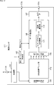
- the pixel 10 in FIG. 1 includes a SPAD 21, a constant current source 22, a transistor 23, and an inverter 24.
- the cathode of the SPAD 21 is connected to the constant current source 22 and also to the input terminal of the inverter 24 and the drain of the transistor 23.
- the anode of the SPAD21 is connected to the power supply voltage VSPAD.
- SPAD21 is a photodiode (single photon avalanche photodiode) that avalanche amplifies the generated electrons and outputs a cathode voltage VS signal when incident light is incident.
- the power supply voltage VSPAD supplied to the anode of the SPAD21 is, for example, a negative bias (negative potential) having the same voltage as the breakdown voltage VBD of the SPAD21.
- the constant current source 22 is composed of, for example, a P-type MOS transistor that operates in a saturation region, and performs passive quenching by acting as a quenching resistance.
- a power supply voltage VE (VE> 0) is supplied to the constant current source 22.
- the constant current source 22 may use a pull-up resistor or the like instead of the P-type MOS transistor.
- the drain of the transistor 23 is connected to the cathode of the SPAD 21, the input terminal of the inverter 24, and the constant current source 22, and the source of the transistor 23 is connected to the ground (GND).
- a gating control signal VG is supplied to the gate of the transistor 23 from a pixel control circuit that drives the pixels.
- a Lo (Low) gating control signal VG is supplied from the pixel control circuit to the gate of the transistor 23.
- a Hi (High) gating control signal VG is supplied from the pixel control circuit to the gate of the transistor 23.
- the inverter 24 outputs a Hi PFout signal when the cathode voltage VS as an input signal is Lo, and outputs a Lo PFout signal when the cathode voltage VS is Hi.
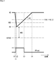
- FIG. 2 is a graph showing a change in the cathode voltage VS of the SPAD 21 and a detection signal PFout according to the incident of a photon.
- the transistor 23 is set to off by the Lo gating control signal VG.
- the power supply voltage VE is supplied to the cathode of the SPAD21 and the power supply voltage VSPAD is supplied to the anode, so that a reverse voltage larger than the breakdown voltage VBD is applied to the SPAD21.
- the cathode voltage VS of SPAD21 becomes lower than 0V, it becomes lower than the breakdown voltage VBD, so the avalanche amplification stops.
- the current generated by the avalanche amplification flows to the constant current source 22 to generate a voltage drop, and the cathode voltage VS becomes lower than the breakdown voltage VBD as the generated voltage drop causes the avalanche.
- the operation of stopping the amplification is the quenching operation.
- the current flowing through the constant current source 22 gradually decreases, and at time t4, the cathode voltage VS returns to the original power supply voltage VE again, and the next new photon is detected. It will be ready (recharge operation).
- a Hi (High) PFout signal is output during the period from time t1 to time t3.
- a Hi gating control signal VG is supplied from the pixel control circuit to the gate of the transistor 23, and the transistor 23 is turned on.
- the cathode voltage VS of the SPAD 21 becomes 0V (GND)
- the voltage between the anode and the cathode of the SPAD 21 becomes equal to or less than the breakdown voltage VBD, so that even if a photon enters the SPAD 21, it does not react.
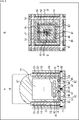
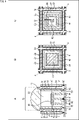
- FIG. 3 is a diagram showing a first configuration example of the pixel 10 using the SPAD 21 described above.
- a in FIG. 3 is a cross-sectional view of the pixel 10 according to the first configuration example
- B in FIG. 3 is a plan view of the pixel 10 according to the first configuration example.
- the cross-sectional view of A in FIG. 3 shows a cross-sectional view taken along the line BB'of B in FIG. 3
- the plan view of B in FIG. 3 shows a plan view taken along the line AA' of FIG. There is.
- the pixel 10 As shown in FIG. 3A, the pixel 10 according to the first configuration example has the on-chip lens 32 on one surface of the semiconductor substrate 31 made of silicon or the like, and the SPAD 21 on the other surface. It has a wiring layer 33 in which wiring for supplying a power supply voltage VE to the cathode and supplying a power supply voltage VSPAD to the anode is formed.
- the surface on which the wiring layer 33 is formed which is the lower side of the semiconductor substrate 31, is the front surface side of the semiconductor substrate 31, and the surface on which the on-chip lens 32 is formed is the back surface side.
- the incident surface on which the reflected light reflected from the object is incident is the back surface side on which the on-chip lens 32 is formed. Therefore, the pixel 10 has a back-illuminated pixel structure that receives incident light on the back surface side of the semiconductor substrate 31.
- the pixel 10 has an n-well 41 below the on-chip lens 32 in the semiconductor substrate 31, and has a high-concentration n-type semiconductor region 42 and a high density in the n-well 41.
- a p-type semiconductor region 43 and a high-concentration n-type semiconductor region 44 are formed.
- the n-well 41 is formed by controlling the impurity concentration of the semiconductor substrate 31 to be a thin n-type (n-), and forms an electric field that transfers electrons generated by the photoelectric conversion in the pixel 10 to the avalanche multiplying region. ..
- a p-well in which the impurity concentration of the semiconductor substrate 31 is controlled to be p-type may be formed.
- the high-concentration n-type semiconductor region 42 is a dense n-type (first conductive type) semiconductor region (first semiconductor region) formed in a predetermined plane region at a predetermined depth from the front surface side of the semiconductor substrate 31. ), And has a substantially T-shaped cross-sectional shape extending in the vertical direction (depth direction) in the central portion of the pixel region, and is formed up to the front surface of the semiconductor substrate 31. Then, at the interface on the front surface side of the semiconductor substrate 31, the high-concentration n-type semiconductor region 42 is connected to the wiring 61 formed in the wiring layer 33. A power supply voltage VE is supplied to the high-concentration n-type semiconductor region 42 via the wiring 61.
- the wiring 61 supplies the power supply voltage VE for forming the avalanche multiplying region to the high-concentration n-type semiconductor region 42 as the cathode electrode.
- the wiring 61 does not exist in the cross section of the AA'line of A in FIG. 3, it is shown in FIG. Wiring 61 is shown in the plan view of B of 3. The illustration of the wiring 61 on the plan view is the same in other drawings described later.
- the power supply voltage VE is supplied to the high-concentration n-type semiconductor region 42 as the cathode electrode by, for example, four wirings 61.
- the number of wirings 61 is not limited to four, and other wirings may be used.
- the high-concentration p-type semiconductor region 43 of FIG. 3A is a dense p-type (second conductive type) semiconductor region (second conductive type) formed by joining to the upper surface of the high-concentration n-type semiconductor region 42 in the semiconductor substrate 31. (Semiconductor domain).
- the avalanche multiplying region is formed by the depletion layer formed in the PN junction region where the high-concentration n-type semiconductor region 42 and the high-concentration p-type semiconductor region 43 are joined.
- the planar shape of the high-concentration n-type semiconductor region 42 is a rectangular shape substantially equivalent to the outer size of the high-concentration n-type semiconductor region 44 in FIG.
- the planar shape of the high-concentration p-type semiconductor region 43 is formed to be slightly smaller than the planar size of the high-concentration n-type semiconductor region 42. This reduces edge breakdown at the ends of the multiplying region.
- the high-concentration n-type semiconductor region 44 (third semiconductor region) is located near the front surface interface of the semiconductor substrate 31 and is separated from the high-concentration n-type semiconductor region 42 as the cathode electrode by a predetermined distance in the plane direction. Is formed in.
- the high-concentration n-type semiconductor region 44 functions as a gettering site, which is a region for capturing and fixing impurities that cause metal contamination.
- the planar shape of the high-concentration n-type semiconductor region 44 is a rectangular shape having a predetermined width, and is an outer periphery of the high-concentration n-type semiconductor region 42 formed in the central portion of the pixel region. It is arranged so as to surround.
- the planar position of the high-concentration n-type semiconductor region 44 is arranged at a position where at least a part of the high-concentration n-type semiconductor region 42 and the high-concentration p-type semiconductor region 43 overlap with the PN junction region.
- the impurity concentration of the high-concentration n-type semiconductor region 44 is, for example, the same as that of the high-concentration n-type semiconductor region 42.
- the high-concentration n-type semiconductor region 44 is not connected to any of the wirings of the wiring layer 33 and is electrically floating.
- the impurity concentration of the n-well 41 is, for example, a low concentration of 1E + 14 / cm 3 or less, and the impurities in the high-concentration n-type semiconductor region 42 and the high-concentration p-type semiconductor region 43 forming the avalanche multiplying region are respectively.
- the concentration is a high concentration of 1E + 16 / cm 3 or more.
- An inter-pixel separation portion 51 that penetrates the semiconductor substrate 31 from the front surface side to the back surface side is formed at the boundary portion between the n-well 41 and the other adjacent pixels 10 in the plane direction.
- the inter-pixel separation portion 51 is formed of, for example, a metal material such as tungsten (W), aluminum (Al), titanium (Ti), titanium nitride (TiN), or a conductive material such as polysilicon, and is adjacent to another pixel. And electrically separate. As shown in FIG. 3B, the inter-pixel separation portion 51 as a whole of the semiconductor substrate 31 is formed in a grid pattern along the pixel boundary.
- An insulating layer 52, a fixed charge film 53, and a hole storage layer 54 are formed in this order on the side wall of the pixel-to-pixel separation portion 51 in the pixel.
- the insulating layer 52 is made of, for example, SiO2.
- the fixed charge film 53 is a negative fixed charge film, and a hole storage region is formed inside the fixed charge film 53 by inducing holes by the fixed charge film 53.
- the hole storage layer 54 is formed in a p-type semiconductor region (p) and stores holes generated by photoelectric conversion. Further, the hole storage layer 54 also has an effect of trapping electrons generated at the interface with the insulating layer 52 and suppressing DCR (dark count rate).
- the hole storage region formed by the fixed charge film 53 and the hole storage layer 54 formed inside the fixed charge film 53 can suppress dark current and suppress DCR.
- PDE Photon Detection Efficiency
- the impurity concentration is particularly controlled to a high concentration (p +), and is regarded as a high concentration p-type semiconductor region 55 (fourth semiconductor region).
- the high-concentration p-type semiconductor region 55 is connected to the wiring 62 formed in the wiring layer 33.
- a power supply voltage VSPAD is applied to the high-concentration p-type semiconductor region 55 via the wiring 62. That is, the wiring 62 supplies the power supply voltage VSPAD to the high-concentration p-type semiconductor region 55 as the anode electrode.
- the hole accumulation layer 54 can be formed by ion implantation or may be formed by solid phase diffusion. In the example of FIG. 3, the hole storage layer 54 is formed only on the side surface of the inter-pixel separation portion 51, but it may also be formed on the interface on the back surface side of the substrate, which is the light incident surface.
- the high-concentration n-type semiconductor region 42 as the cathode electrode is a pixel at the front surface side interface of the semiconductor substrate 31. It is formed with a small planar size only in the center of the region.
- the high-concentration p-type semiconductor region 55 as the anode electrode is formed along the outer peripheral portion of the rectangular pixel region.
- a high-concentration n-type semiconductor region 44 that functions as a gettering site is electrically formed in a floating state between the high-concentration n-type semiconductor region 42 and the high-concentration p-type semiconductor region 55.
- the electric field between the cathode and the anode can be relaxed, and the generation of electrons as a dark current component can be prevented. Further, it is possible to reduce an unintended edge breakdown that occurs when the distance between the cathode and the anode is narrowed when the pixel 10 is miniaturized.
- the impurity concentration of the high-concentration n-type semiconductor region 44 that functions as a gettering site is set to the same concentration as that of the high-concentration n-type semiconductor region 42, but it does not necessarily have to be the same, and it is set to a different concentration. May be good.
- planar shape of the high-concentration n-type semiconductor region 44 that functions as a gettering site is rectangular, it may be a shape that can be arranged between the high-concentration n-type semiconductor region 42 and the high-concentration p-type semiconductor region 55. It may be a polygonal shape or an annular shape, for example. Further, the polygonal shape may have rounded corners.
- the first configuration example shown in FIG. 3 is an example of a structure that reads out electrons as a signal charge (carrier), but it can also be a structure that reads out holes.
- the high-concentration n-type semiconductor region 42 is changed to the high-concentration p-type semiconductor region, and the high-concentration p-type semiconductor region 43 is changed to the high-concentration n-type semiconductor region. Further, the high-concentration p-type semiconductor region 55 is changed to the high-concentration n-type semiconductor region.
- a power supply voltage VSPAD is applied from the wiring 61 to the contact portion changed from the high-concentration n-type semiconductor region 42 to the high-concentration p-type semiconductor region, and the high-concentration p-type semiconductor region 55 is changed to the high-concentration n-type semiconductor region.
- a power supply voltage VE is applied to the modified contact portion from the wiring 62.
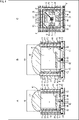
- FIG. 4 is a diagram showing a second configuration example of the pixel 10 using the above-mentioned SPAD 21.
- a in FIG. 4 is a cross-sectional view of the pixel 10 according to the second configuration example
- B in FIG. 4 is a plan view of the pixel 10 according to the second configuration example.
- the cross-sectional view of A in FIG. 4 shows the cross-sectional view taken along the line B-B'of B of FIG. 4, and the plan view of B of FIG. 4 shows the plan view of the line A-A' of FIG. There is.
- the second configuration example of FIG. 4 differs from the first configuration example of FIG. 3 in that the embedded insulating films 81 and 82 are newly provided, and is common to the first configuration example of FIG. 3 in other respects. do.
- the embedded insulating films 81 and 82 are so-called STIs (Shallow Trench Isolation).
- the embedded insulating film 81 is formed inside between the high-concentration n-type semiconductor region 42 which is a cathode electrode and the high-concentration n-type semiconductor region 44 which is a gettering site.
- the high-concentration n-type semiconductor region 42 is arranged in a rectangular shape surrounding the high-concentration n-type semiconductor region 42 with a predetermined width.
- the embedded insulating film 82 has a high inner height between the high-concentration n-type semiconductor region 44, which is a gettering site, and the high-concentration p-type semiconductor region 55, which is an anode electrode.
- the density n-type semiconductor region 44 is arranged in a rectangular shape surrounding the region 44 with a predetermined width.
- the high-concentration n-type semiconductor region 42 as the cathode electrode is formed only in the central portion of the pixel region in a small plane size, and the anode.
- the high-concentration p-type semiconductor region 55 as an electrode is formed along the outer peripheral portion of a rectangular pixel region.
- a high-concentration n-type semiconductor region 44 that functions as a gettering site is electrically formed in a floating state between the high-concentration n-type semiconductor region 42 and the high-concentration p-type semiconductor region 55.
- the electric field between the cathode and the anode can be relaxed, and the generation of electrons as a dark current component can be prevented. Further, it is possible to reduce an unintended edge breakdown that occurs when the distance between the cathode and the anode is narrowed when the pixel 10 is miniaturized.
- the pixel 10 according to the second configuration example is provided with an embedded insulating film 81 between the high-concentration n-type semiconductor region 42 as a cathode electrode and the high-concentration n-type semiconductor region 44 as a gettering site, and is provided with a gettering site.
- An embedded insulating film 82 is provided between the high-concentration n-type semiconductor region 44 and the high-concentration p-type semiconductor region 55, which is an anode electrode.
- the physically inserted embedded insulating films 81 and 82 can further relax the electric field between the cathode and the anode, further reducing the unintended edge breakdown caused by the narrowing of the distance between the cathode and anode electrodes. It can be reduced.
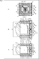
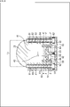
- FIG. 5 is a diagram showing a third configuration example of the pixel 10 using the SPAD 21 described above.
- a and B in FIG. 5 are cross-sectional views of the pixel 10 according to the third configuration example
- C in FIG. 5 is a plan view of the pixel 10 according to the third configuration example.
- the cross-sectional view of A in FIG. 5 shows a cross-sectional view taken along the line AA'of C of FIG. 5, and the cross-sectional view of B of FIG. 5 shows a cross-sectional view taken along the line B-B' of FIG.
- the plan view of C in FIG. 5 shows a plan view of A'A'line of FIG. 5 and B-B'line of B of FIG.
- the formation position of the high-concentration p-type semiconductor region 55 as the anode electrode is different from that of the first configuration example shown in FIG. That is, the high-concentration p-type semiconductor region 55 was formed on the entire outer peripheral portion of the rectangular pixel region as shown in FIG. 3B in the first configuration example, but in the third configuration example of FIG. 5, it is rectangular. It is formed in a triangular shape at each corner of the four corners of the pixel area of.
- the high-concentration n-type semiconductor region 44 that functions as a gettering site has a rectangular shape in which each corner of the four corners is cut off diagonally in a plan view. As a result, the distance between the high-concentration p-type semiconductor region 55 arranged at the corners of the four corners and the high-concentration n-type semiconductor region 44 is maintained by a certain amount.
- a wide distance DX between the anode and the cathode is secured, and a region of the high-concentration n-type semiconductor region 44 as a gettering site is secured. Can be done. Then, the high-concentration n-type semiconductor region 44 is electrically formed in a floating state, the electric field between the cathode and the anode can be relaxed, and the generation of electrons as a dark current component can be prevented. Further, it is possible to reduce an unintended edge breakdown that occurs when the distance between the cathode and the anode is narrowed when the pixel 10 is miniaturized.
- the high-concentration p-type semiconductor region 55 which is the anode electrode, is arranged in a triangular shape at each corner of the four corners of the rectangular pixel region, so that the high-concentration n-type semiconductor region 42, which is the cathode electrode, is formed.
- the distance can be secured wider.
- the high-concentration p-type semiconductor region 55 as the anode electrode does not exist in the central portion of the outer peripheral portion of the rectangular pixel region, the region of the high-concentration n-type semiconductor region 44 as the gettering site is expanded to the outer peripheral portion. And can expand the area of the gettering site.
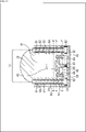
- FIG. 6 is a diagram showing a fourth configuration example of the pixel 10 using the SPAD 21 described above.
- a and B in FIG. 6 are cross-sectional views of the pixel 10 according to the fourth configuration example
- C in FIG. 6 is a plan view of the pixel 10 according to the fourth configuration example.
- the cross-sectional view of A in FIG. 6 shows the cross-sectional view taken along the line AA'of C of FIG. 6, and the cross-sectional view of B of FIG. 6 shows the cross-sectional view taken along the line B-B' of FIG.
- the plan view of C in FIG. 6 shows a plan view in the AA'line of A in FIG. 6 and the B-B'line of B in FIG.
- the formation position of the high-concentration n-type semiconductor region 44 as a gettering site is different from that of the third configuration example shown in FIG. That is, in the third configuration example, as shown in FIG. 5B, the high-concentration n-type semiconductor region 44 includes the high-concentration n-type semiconductor region 42 as a cathode electrode formed in the central portion of the rectangular pixel region. Although it was formed as one surrounding region, in the fourth configuration example of FIG. 6, as shown in C of FIG. 6, the outside of the high-concentration n-type semiconductor region 42 in the central portion of the pixel region in the vertical and horizontal directions. It is divided into four regions. It is the same as the third configuration example shown in FIG. 5, except for the formation position of the high-concentration n-type semiconductor region 44.
- the high-concentration n-type semiconductor region 44 as a gettering site is arranged so as to surround the entire outer periphery of the high-concentration n-type semiconductor region 42 as a cathode electrode formed in the central portion of the pixel region.
- the high-concentration n-type semiconductor region 44 is arranged outside the high-concentration n-type semiconductor region 42 in the central portion of the pixel region in the vertical and horizontal directions, but is in the diagonal direction of the rectangular pixel region. It may be arranged outside in the diagonal direction upward to the right and diagonally upward to the left.
- the distance DX between the anode and the cathode is secured wider, and the region of the high-concentration n-type semiconductor region 44 as a gettering site is secured. be able to.
- the high-concentration n-type semiconductor region 44 formed so as to be electrically in a floating state functions as a gettering site, so that the electric field between the cathode and the anode can be relaxed and the electrons serving as dark current components can be relaxed. Can be prevented. Further, it is possible to reduce an unintended edge breakdown that occurs when the distance between the cathode and the anode is narrowed when the pixel 10 is miniaturized.
- the region of the high-concentration n-type semiconductor region 44 as the gettering site is surrounded by the outer periphery. It can be expanded to the department, and the area of the gettering site can be expanded.
- FIG. 7 is a diagram showing a fifth configuration example of the pixel 10 using the above-mentioned SPAD 21.
- a and B in FIG. 7 are cross-sectional views of the pixel 10 according to the fifth configuration example
- C in FIG. 7 is a plan view of the pixel 10 according to the fifth configuration example.
- the cross-sectional view of A in FIG. 7 shows a cross-sectional view taken along the line AA'of C of FIG. 7
- the cross-sectional view of B of FIG. 7 shows a cross-sectional view taken along the line B-B'of C of FIG.
- the plan view of C in FIG. 7 shows a plan view taken along the line A-A'of A in FIG. 7 and the line B-B'of B in FIG.
- the fifth configuration example of FIG. 7 has a configuration in which the embedded insulating films 81 and 82 similar to the second configuration example of FIG. 4 are newly added to the third configuration example shown in FIG.
- the second configuration example of FIG. 4 is a configuration in which the high-concentration p-type semiconductor region 55 as an anode electrode is arranged on the entire outer peripheral portion of the rectangular pixel region
- the fifth configuration example of FIG. 7 is a configuration.
- the high-concentration p-type semiconductor region 55 as the anode electrode is arranged in a triangular shape at each corner of the four corners of the rectangular pixel region. Therefore, the embedded insulating film 82 is formed not in the entire outer periphery of the high-concentration n-type semiconductor region 44 but only in the diagonal direction in which the high-concentration p-type semiconductor region 55 is formed.
- the embedded insulating film 81 has a predetermined inner high-concentration n-type semiconductor region 42 between the high-concentration n-type semiconductor region 42 as the cathode electrode and the high-concentration n-type semiconductor region 44 as the gettering site. It is arranged in a rectangular shape surrounded by a width.
- the embedded insulating film 82 is divided into four regions in the diagonal direction of the pixel region between the high-concentration n-type semiconductor region 44 as a gettering site and the high-concentration p-type semiconductor region 55 as an anode electrode. Have been placed.
- the distance DX between the anode and the cathode is secured wider, and the region of the high-concentration n-type semiconductor region 44 as a gettering site is secured. be able to.
- the high-concentration n-type semiconductor region 44 formed so as to be electrically in a floating state functions as a gettering site, so that the electric field between the cathode and the anode can be relaxed and the electrons serving as dark current components can be relaxed. Can be prevented. Further, it is possible to reduce an unintended edge breakdown that occurs when the distance between the cathode and the anode is narrowed when the pixel 10 is miniaturized.
- the region of the high-concentration n-type semiconductor region 44 which is a gettering site, is surrounded by the outer periphery. It can be expanded to the department, and the area of the gettering site can be expanded.
- an embedded insulating film 81 is provided between the high-concentration n-type semiconductor region 42 as the cathode electrode and the high-concentration n-type semiconductor region 44 as the gettering site, and the high-concentration n-type semiconductor region 44 as the gettering site is provided.
- FIG. 8 is a diagram showing a sixth configuration example of the pixel 10 using the SPAD 21 described above.
- a in FIG. 8 is a cross-sectional view of the pixel 10 according to the sixth configuration example
- B and C in FIG. 8 are plan views of the pixel 10 according to the sixth configuration example.
- the cross-sectional view of A in FIG. 8 shows a cross-sectional view taken along the line AA'of B and C of FIG. 8, and the plan view of B of FIG. Shown, the plan view of C in FIG. 8 shows the plan view of A in FIG. 8 on the YY'line.
- the positions of the high-concentration n-type semiconductor region 42 and the high-concentration p-type semiconductor region 43 forming the avalanche multiplying region in the substrate depth direction are shown in FIG. It is formed at a deeper position in the substrate as compared with one configuration example. Further, with the change in the substrate depth position of the PN junction region, the high-concentration n-type semiconductor region 44 as a gettering site is also formed from the substrate front surface to a deeper position in the substrate.
- the substrate depth position of the PN junction region of the high-concentration n-type semiconductor region 42 and the high-concentration p-type semiconductor region 43 is, for example, about 1/4 to 1/2 of the substrate thickness from the front surface of the semiconductor substrate 31. It can be a corresponding position.
- Other configurations of the pixel 10 according to the sixth configuration example are the same as those of the first configuration example shown in FIG.
- the high-concentration n-type semiconductor region 42 and the high-concentration p-type semiconductor region 43 that form the avalanche multiplier region are formed at a deep position on the semiconductor substrate 31, the high-concentration n-type that functions as a gettering site. Since the semiconductor region 44 can also be formed deep in the depth direction of the substrate, the gettering site can be formed not only on the surface of the substrate but also in the depth direction.
- the distance DX between the anode and the cathode can be secured wider, and the region of the high-concentration n-type semiconductor region 44 as a gettering site can be secured. Then, the high-concentration n-type semiconductor region 44 formed so as to be electrically in a floating state functions as a gettering site, so that the electric field between the cathode and the anode can be relaxed and the electrons serving as dark current components can be relaxed. Can be prevented. Further, it is possible to reduce an unintended edge breakdown that occurs when the distance between the cathode and the anode is narrowed when the pixel 10 is miniaturized.
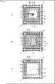
- Pixel 7th configuration example> 9 and 10 are views showing a seventh configuration example of the pixel 10 using the SPAD 21 described above.
- FIG. 9 is a cross-sectional view of the pixel 10 according to the seventh configuration example
- FIG. 10 is a plan view of the pixel 10 according to the seventh configuration example.
- the cross-sectional view of FIG. 9 shows the cross-sectional view taken along the line AA'of FIG. 10, the plan view of A of FIG. 10 shows the plan view of the line X-X'of FIG.
- the figure shows the plan view in the YY'line of FIG. 9, and the plan view of C in FIG. 10 shows the plan view in the ZZ'line of FIG.
- the seventh configuration example of FIG. 9 is common to the sixth configuration example of FIG. 8 in that the high-concentration n-type semiconductor region 44 functioning as a gettering site is deeply formed in the substrate depth direction. As a result, gettering sites can be formed not only on the surface of the substrate but also in the depth direction.
- the high-concentration n-type semiconductor region 44 as a gettering site is a PN junction between the high-concentration n-type semiconductor region 42 forming the avalanche multiplication region and the high-concentration p-type semiconductor region 43.
- the sixth configuration example of FIG. 8 is formed to a position deeper than the depth position of the PN junction region. It differs from the configuration example.
- the high-concentration n-type semiconductor region 44 of the sixth configuration example in FIG. 8 was arranged at a position where at least a part overlaps with the PN junction region in a plan view.
- the high-concentration n-type semiconductor region 44 of the seventh configuration example is arranged outside the PN junction region in a plan view as shown in FIG. 10B.
- the distance DX between the anode and the cathode can be secured wider, and the region of the high-concentration n-type semiconductor region 44 as a gettering site can be secured. Then, the high-concentration n-type semiconductor region 44 formed so as to be electrically in a floating state functions as a gettering site, so that the electric field between the cathode and the anode can be relaxed and the electrons serving as dark current components can be relaxed. Can be prevented. Further, it is possible to reduce an unintended edge breakdown that occurs when the distance between the cathode and the anode is narrowed when the pixel 10 is miniaturized.
- Pixel 8th configuration example> 11 and 12 are views showing an eighth configuration example of the pixel 10 using the SPAD 21 described above.
- FIG. 11 is a cross-sectional view of the pixel 10 according to the eighth configuration example
- FIG. 12 is a plan view of the pixel 10 according to the eighth configuration example.
- the cross-sectional view of FIG. 11 shows the cross-sectional view taken along the line AA'of FIG. 12, the plan view of A of FIG. 12 shows the plan view of the line X-X'of FIG.
- the figure shows the plan view in the YY'line of FIG. 11, and the plan view of C in FIG. 12 shows the plan view in the ZZ'line of FIG.
- the eighth configuration example of FIG. 11 is common to the seventh configuration example of FIG. 9 in that the high-concentration n-type semiconductor region 44 that functions as a gettering site is deeply formed in the substrate depth direction. As a result, gettering sites can be formed not only on the surface of the substrate but also in the depth direction.
- the difference between the 8th configuration example of FIG. 11 and the 7th configuration example shown in FIG. 9 is that the high-concentration n-type semiconductor region 44 of the 7th configuration example shown in FIG. 9 is located deeper than the PN junction region.
- the depth is the same as that of the PN junction region. It should be noted that the depth of the PN junction region does not have to be exactly the same, but may be substantially the same.
- the position of the high-concentration n-type semiconductor region 44 in the substrate depth direction is formed deeper than that of the high-concentration p-type semiconductor region 43 in the seventh configuration example shown in FIG.
- the position is set so as not to exceed the depth of the high-concentration p-type semiconductor region 43 constituting the PN junction region.
- the distance DX between the anode and the cathode can be secured wider, and the region of the high-concentration n-type semiconductor region 44 as a gettering site can be secured. Then, the high-concentration n-type semiconductor region 44 formed so as to be electrically in a floating state functions as a gettering site, so that the electric field between the cathode and the anode can be relaxed and the electrons serving as dark current components can be relaxed. Can be prevented. Further, it is possible to reduce an unintended edge breakdown that occurs when the distance between the cathode and the anode is narrowed when the pixel 10 is miniaturized.
- Ninth configuration example of pixel> 13 and 14 are views showing a ninth configuration example of the pixel 10 using the SPAD 21 described above.
- FIG. 13 is a cross-sectional view of the pixel 10 according to the ninth configuration example
- FIG. 14 is a plan view of the pixel 10 according to the ninth configuration example.
- the cross-sectional view of FIG. 13 shows the cross-sectional view taken along the line AA'of FIG. 14, the plan view of A of FIG. 14 shows the plan view of the line XX'of FIG.
- the figure shows the plan view in the YY'line of FIG. 13, and the plan view of C in FIG. 14 shows the plan view in the ZZ'line of FIG.
- both the high-concentration n-type semiconductor region 44 of the first configuration example shown in FIG. 3 and the high-concentration n-type semiconductor region 44 of the eighth configuration example shown in FIG. 11 are shown. It has a configuration including.
- the high-concentration n-type semiconductor region 44A in the ninth configuration example is the high-concentration n-type semiconductor region 42 and the high-concentration p that form the avalanche multiplication region in a plan view, as in the first configuration example shown in FIG. It is arranged at a position where at least a part of the PN junction region of the type semiconductor region 43 overlaps.
- the high-concentration n-type semiconductor region 44B in the ninth configuration example is the high-concentration n-type semiconductor region 42 and the high-concentration p that form the avalanche multiplication region in a plan view, as in the eighth configuration example shown in FIG. It is arranged outside the PN junction region of the type semiconductor region 43, and is formed to substantially the same depth as the PN junction region in a cross-sectional view.
- the position in the depth direction may be formed deeper than the PN junction region as in the seventh configuration example shown in FIG. That is, the position of the high-concentration n-type semiconductor region 44B in the depth direction may be at least substantially the same depth as the PN junction region.
- the distance DX between the anode and the cathode can be secured wider, and the region of the high-concentration n-type semiconductor region 44 as a gettering site can be secured. Then, the high-concentration n-type semiconductor region 44 formed so as to be electrically in a floating state functions as a gettering site, so that the electric field between the cathode and the anode can be relaxed and the electrons serving as dark current components can be relaxed. Can be prevented. Further, it is possible to reduce an unintended edge breakdown that occurs when the distance between the cathode and the anode is narrowed when the pixel 10 is miniaturized.
- the high-concentration n-type semiconductor region 44A arranged on the outer periphery of the high-concentration n-type semiconductor region 42 in the region near the front surface of the substrate and the outer periphery of the avalanche multiplying region have a height of substantially the same depth as the avalanche multiplying region.
- FIG. 15 is a diagram showing a tenth configuration example of the pixel 10 using the SPAD 21 described above.
- a in FIG. 15 is a cross-sectional view of the pixel 10 according to the tenth configuration example
- B in FIG. 15 is a plan view of the pixel 10 according to the tenth configuration example.
- the cross-sectional view of A in FIG. 15 shows a cross-sectional view taken along the line B-B'of B of FIG. 15, and the plan view of B of FIG. 15 shows the plan view of the line A-A' of FIG. There is.
- a color filter 91 that transmits a wavelength corresponding to a predetermined color such as R (Red), G (Green), (Blue) is formed on the back surface side of the semiconductor substrate 31, and a color is formed. It differs from the first configuration example of FIG. 3 in that the on-chip lens 32 is formed on the filter 91, and is common to the first configuration example of FIG. 3 in other respects.
- the color arrangement of the color filter 91 is, for example, arranged in a so-called bayer arrangement, but the arrangement format is not limited to the bayer arrangement. Further, the type of color is not limited to R, G, and B, and may be other colors such as C (Cyan), M (Magenta), and Y (Yellow).
- the color filter 91 transmits both visible light and infrared light of a predetermined color.
- the number of photons transmitted through the color filters 91 such as R, G, B and received is counted in a predetermined exposure period, and the count value is output as a luminance value. Therefore, it can also be used as an image sensor that outputs data for viewing. Further, since the color filter 91 also transmits infrared light, it is possible to output distance measurement data as a distance measurement sensor.
- the distance DX between the anode and the cathode can be secured wider, and the region of the high-concentration n-type semiconductor region 44 as a gettering site can be secured. Then, the high-concentration n-type semiconductor region 44 formed so as to be electrically in a floating state functions as a gettering site, so that the electric field between the cathode and the anode can be relaxed and the electrons serving as dark current components can be relaxed. Can be prevented. Further, it is possible to reduce an unintended edge breakdown that occurs when the distance between the cathode and the anode is narrowed when the pixel 10 is miniaturized.
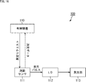
- FIG. 16 is a block diagram showing a configuration example of a distance measuring system using the pixels 10 according to the first to tenth configuration examples described above.
- the distance measuring system 100 of FIG. 16 includes a control device 110, a distance measuring sensor 111, an LD 112, and a light emitting unit 113.
- the control device 110 is a device that controls the distance measuring sensor 111.
- the control device 110 supplies, for example, a measurement request requesting execution of measurement to the distance measuring sensor 111 based on a command from a higher-level host device. Then, the control device 110 acquires the measurement data, which is the result of the measurement data executed by the distance measuring sensor 111 in response to the measurement request, from the distance measuring sensor 111.
- the distance measuring sensor 111 executes measurement of the distance to the subject by, for example, the ToF method in response to the measurement request from the control device 110, and outputs the measurement data as a result to the control device 110.
- the distance measuring sensor 111 is a light receiving element including the pixel 10 having any of the configurations of the first to tenth configurations described above.
- the distance measuring sensor 111 controls the light emitting unit 113 as necessary to emit the irradiation light at the time of measurement.
- the ranging sensor 111 supplies a predetermined emission pulse to the LD 112.
- the LD 112 is a laser driver that drives the light emitting unit 113, drives the light emitting unit 113 based on the light emitting pulse from the ranging sensor 111, and outputs the irradiation light from the light emitting unit 113.
- the light emitting unit 113 is composed of, for example, a VCSEL LED (Vertical Cavity Surface Emitting LASER LED) or the like, and emits irradiation light by driving the LD 112.
- the irradiation light for example, infrared light (IR light) having a wavelength in the range of about 850 nm to 940 nm is used.
- FIG. 17 is a block diagram showing a first configuration example of the distance measuring sensor 111.
- the first configuration example shown in FIG. 17 is a configuration in which the distance measuring sensor 111 has any of the above-mentioned first to ninth configuration examples as the pixel 10.
- the distance measuring sensor 111 includes a control unit 141, a light emitting timing control unit 142, a SPAD pixel array unit 143, a SPAD control circuit 144, a read circuit 145, a data processing unit 146, an output IF 147, and input / output terminals 151a to 151c.
- the control unit 141 controls the entire operation of the distance measuring sensor 111.
- the control unit 141 performs predetermined communication such as reception of a measurement request and transmission of measurement data with the control device 110.
- the distance measuring sensor 111 can operate all the pixels 10 in the SPAD pixel array unit 143 (active pixels), or can operate only a part of the pixels 10 such as a plurality of lines.
- the control unit 141 supplies an active control signal for controlling which pixel 10 in the SPAD pixel array unit 143 is operated to the SPAD control circuit 144.
- the light emission timing control unit 142 generates a light emission pulse that controls the light emission timing of the irradiation light based on the control from the control unit 141, and outputs the light emission pulse to the LD 112 via the input / output terminal 151b. Further, the light emission timing control unit 142 also supplies the generated light emission pulse to the data processing unit 146.
- the SPAD pixel array unit 143 has a plurality of pixels 10 arranged two-dimensionally in a matrix, and supplies a pixel signal corresponding to the reflected light detected in each pixel 10 to the readout circuit 145.
- the configuration of the pixel 10 any one of the first to ninth configuration examples described above is adopted.
- the SPAD control circuit 144 switches between active pixels and inactive pixels for each pixel 10 of the SPAD pixel array unit 143 based on the active control signal supplied from the control unit 141.
- An active pixel is a pixel that detects the incident of a photon
- an inactive pixel is a pixel that does not detect the incident of a photon. Therefore, the SPAD control circuit 144 controls the on / off of the light receiving operation of each pixel 10 of the SPAD pixel array unit 143.
- the SPAD control circuit 144 at least a part of the plurality of pixels 10 of the SPAD pixel array unit 143 is set as active pixels and the remaining pixels 10 are non-active pixels at a predetermined timing according to the light emission pulse from the light emission timing control unit 142. Controls the active pixel.
- all the pixels 10 of the SPAD pixel array unit 143 may be used as active pixels.
- the readout circuit 145 supplies the pixel signal supplied from each pixel 10 of the SPAD pixel array unit 143 to the data processing unit 146.
- the data processing unit 146 has a histogram generation circuit 171 and a distance calculation unit 172.
- the histogram generation circuit 171 is based on the emission of the irradiation light repeatedly executed a predetermined number of times (for example, several times to several hundred times) and the reception of the reflected light, and the flight time (count) until the reflected light is received. Value) histogram is created for each pixel. Data about the created histogram (hereinafter referred to as histogram data) is supplied to the distance calculation unit 172.
- the distance calculation unit 172 performs noise removal, histogram peak detection, and the like on the histogram data supplied from the histogram generation circuit 171.
- the distance calculation unit 172 calculates the flight time until the light emitted from the light emitting unit 113 is reflected by the subject and returns based on the peak value of the detected histogram, and the flight time is calculated from the calculated flight time.
- the distance to the subject is calculated for each pixel.
- the calculated distance data is supplied to the output IF 147.
- the output IF 147 stores the data of the distance to the subject calculated for each pixel in a predetermined data format, and outputs it as measurement data to the control device 110 via the input / output terminal 151c.
- the distance measuring sensor 111 of FIG. 17 has the above configuration, and outputs the result of measuring the distance to the subject in response to the measurement request from the control device 110 to the control device 110 as measurement data.
- FIG. 18 is a block diagram showing a second configuration example of the distance measuring sensor 111.
- the second configuration example shown in FIG. 18 is a configuration in which the distance measuring sensor 111 has the above-mentioned tenth configuration example as the pixel 10.
- the distance measuring sensor 111 according to the second configuration example of FIG. 18 has a different configuration of the data processing unit 146, and the others are the same.
- the data processing unit 146 is composed of a photon count circuit 181 and an image data processing unit 182.
- the photon counting circuit 181 counts the number of times the SPAD of each pixel 10 in the SPAD pixel array unit 143 reacts within a predetermined period, that is, the number of times the photon is incident, for each pixel. Then, the photon count circuit 181 supplies the count result to the image data processing unit 182.
- the image data processing unit 182 generates image data (viewing data) in which the photon count result measured in each pixel 10 is used as a pixel value (brightness value) according to the amount of received light, and supplies the image data (viewing data) to the output IF 147.
- the output IF 147 stores the viewing data calculated for each pixel in a predetermined data format, and outputs the measurement data to the control device 110 via the input / output terminal 151c.
- the distance measuring sensor 111 of FIG. 18 has the above configuration, and in response to a measurement request from the control device 110, the control device uses image data having a pixel value (brightness value) according to the amount of light received as measurement data. Output to 110.
- the distance measuring sensor 111 of FIGS. 17 and 18 includes any of the pixels 10 according to the first to tenth configuration examples as pixels two-dimensionally arranged in a matrix in the SPAD pixel array unit 143.
- the electric field between the cathode and the anode can be relaxed, and the generation of electrons as a dark current component can be prevented.
- the data processing unit 146 of the distance measuring sensor 111 may be configured to include a histogram generation circuit 171 and a distance calculation unit 172, and a photon count circuit 181 and an image data processing unit 182. In this case, as the measurement data, the distance measurement data and the viewing data can be executed and output in a time-division manner.
- the ranging system 100 of FIG. 16 can be mounted on electronic devices such as smartphones, tablet terminals, mobile phones, personal computers, game machines, television receivers, wearable terminals, digital still cameras, and digital video cameras. ..
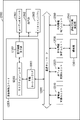
- FIG. 19 is a block diagram showing a configuration example of a smartphone equipped with the distance measuring system 100 of FIG. 16 as a distance measuring module.
- the smartphone 601 has a distance measuring module 602, an image pickup device 603, a display 604, a speaker 605, a microphone 606, a communication module 607, a sensor unit 608, a touch panel 609, and a control unit 610 via a bus 611. Connected and configured. Further, the control unit 610 has functions as an application processing unit 621 and an operation system processing unit 622 by executing a program by the CPU.
- the distance measuring system 100 of FIG. 16 is applied to the distance measuring module 602.
- the distance measurement module 602 is arranged in front of the smartphone 601 and performs distance measurement for the user of the smartphone 601 to measure the depth value of the surface shape of the user's face, hand, finger, etc. as the distance measurement result. Can be output as.
- the image pickup device 603 is arranged in front of the smartphone 601 and takes an image of the user of the smartphone 601 as a subject to acquire an image of the user. Although not shown, the image pickup device 603 may be arranged on the back surface of the smartphone 601.
- the display 604 displays an operation screen for processing by the application processing unit 621 and the operation system processing unit 622, an image captured by the image pickup device 603, and the like.
- the communication module 607 communicates via the communication network.
- the sensor unit 608 senses speed, acceleration, proximity, etc., and the touch panel 609 acquires a touch operation by the user on the operation screen displayed on the display 604.
- the application processing unit 621 performs processing for providing various services by the smartphone 601. For example, the application processing unit 621 can create a face by computer graphics that virtually reproduces the user's facial expression based on the depth supplied from the distance measuring module 602, and can perform a process of displaying the face on the display 604. Further, the application processing unit 621 can perform a process of creating, for example, three-dimensional shape data of an arbitrary three-dimensional object based on the depth supplied from the distance measuring module 602.
- the operation system processing unit 622 performs processing for realizing the basic functions and operations of the smartphone 601. For example, the operation system processing unit 622 can perform a process of authenticating the user's face and unlocking the smartphone 601 based on the depth value supplied from the distance measuring module 602. Further, the operation system processing unit 622 performs a process of recognizing a user's gesture based on the depth value supplied from the distance measuring module 602, and performs a process of inputting various operations according to the gesture. Can be done.
- the smartphone 601 configured in this way, by applying the above-mentioned distance measuring system 100 as the distance measuring module, for example, the distance to a predetermined object as a subject is measured and output as distance measuring data. be able to. Also, in the viewing mode, viewing data can be output.
- the technique according to the present disclosure can be applied to various products.
- the technology according to the present disclosure is realized as a device mounted on a moving body of any kind such as an automobile, an electric vehicle, a hybrid electric vehicle, a motorcycle, a bicycle, a personal mobility, an airplane, a drone, a ship, and a robot. You may.
- FIG. 20 is a block diagram showing a schematic configuration example of a vehicle control system, which is an example of a mobile control system to which the technique according to the present disclosure can be applied.
- the vehicle control system 12000 includes a plurality of electronic control units connected via the communication network 12001.
- the vehicle control system 12000 includes a drive system control unit 12010, a body system control unit 12020, an outside information detection unit 12030, an in-vehicle information detection unit 12040, and an integrated control unit 12050.
- a microcomputer 12051, an audio image output unit 12052, and an in-vehicle network I / F (interface) 12053 are shown as a functional configuration of the integrated control unit 12050.
- the drive system control unit 12010 controls the operation of the device related to the drive system of the vehicle according to various programs.
- the drive system control unit 12010 has a driving force generator for generating a driving force of a vehicle such as an internal combustion engine or a driving motor, a driving force transmission mechanism for transmitting the driving force to the wheels, and a steering angle of the vehicle. It functions as a control device such as a steering mechanism for adjusting and a braking device for generating braking force of the vehicle.
- the body system control unit 12020 controls the operation of various devices mounted on the vehicle body according to various programs.
- the body system control unit 12020 functions as a keyless entry system, a smart key system, a power window device, or a control device for various lamps such as headlamps, back lamps, brake lamps, turn signals or fog lamps.
- the body system control unit 12020 may be input with radio waves transmitted from a portable device that substitutes for the key or signals of various switches.
- the body system control unit 12020 receives inputs of these radio waves or signals and controls a vehicle door lock device, a power window device, a lamp, and the like.
- the vehicle outside information detection unit 12030 detects information outside the vehicle equipped with the vehicle control system 12000.
- the image pickup unit 12031 is connected to the vehicle outside information detection unit 12030.
- the vehicle outside information detection unit 12030 causes the image pickup unit 12031 to capture an image of the outside of the vehicle and receives the captured image.
- the vehicle outside information detection unit 12030 may perform object detection processing or distance detection processing such as a person, a vehicle, an obstacle, a sign, or a character on the road surface based on the received image.
- the image pickup unit 12031 is an optical sensor that receives light and outputs an electric signal according to the amount of the light received.
- the image pickup unit 12031 can output an electric signal as an image or can output it as distance measurement information. Further, the light received by the image pickup unit 12031 may be visible light or invisible light such as infrared light.
- the in-vehicle information detection unit 12040 detects the in-vehicle information.
- a driver state detection unit 12041 that detects a driver's state is connected to the vehicle interior information detection unit 12040.
- the driver state detection unit 12041 includes, for example, a camera that images the driver, and the in-vehicle information detection unit 12040 determines the degree of fatigue or concentration of the driver based on the detection information input from the driver state detection unit 12041. It may be calculated, or it may be determined whether or not the driver has fallen asleep.
- the microcomputer 12051 calculates the control target value of the driving force generator, the steering mechanism, or the braking device based on the information inside and outside the vehicle acquired by the vehicle exterior information detection unit 12030 or the vehicle interior information detection unit 12040, and the drive system control unit.
- a control command can be output to 12010.
- the microcomputer 12051 realizes ADAS (Advanced Driver Assistance System) functions including vehicle collision avoidance or impact mitigation, follow-up driving based on inter-vehicle distance, vehicle speed maintenance driving, vehicle collision warning, vehicle lane deviation warning, and the like. It is possible to perform cooperative control for the purpose of.
- ADAS Advanced Driver Assistance System
- the microcomputer 12051 controls the driving force generating device, the steering mechanism, the braking device, and the like based on the information around the vehicle acquired by the vehicle exterior information detection unit 12030 or the vehicle interior information detection unit 12040. It is possible to perform coordinated control for the purpose of automatic driving that runs autonomously without depending on the operation.
- the microcomputer 12051 can output a control command to the body system control unit 12020 based on the information outside the vehicle acquired by the vehicle outside information detection unit 12030.
- the microcomputer 12051 controls the headlamps according to the position of the preceding vehicle or the oncoming vehicle detected by the outside information detection unit 12030, and performs cooperative control for the purpose of anti-glare such as switching the high beam to the low beam. It can be carried out.
- the audio image output unit 12052 transmits an output signal of at least one of audio and an image to an output device capable of visually or audibly notifying information to the passenger or the outside of the vehicle.
- an audio speaker 12061, a display unit 12062, and an instrument panel 12063 are exemplified as output devices.
- the display unit 12062 may include, for example, at least one of an onboard display and a head-up display.
- FIG. 21 is a diagram showing an example of the installation position of the imaging unit 12031.
- the vehicle 12100 has image pickup units 12101, 12102, 12103, 12104, 12105 as image pickup units 12031.
- the image pickup units 12101, 12102, 12103, 12104, 12105 are provided, for example, at positions such as the front nose, side mirrors, rear bumpers, back doors, and the upper part of the windshield in the vehicle interior of the vehicle 12100.
- the image pickup unit 12101 provided on the front nose and the image pickup section 12105 provided on the upper part of the windshield in the vehicle interior mainly acquire an image in front of the vehicle 12100.
- the image pickup units 12102 and 12103 provided in the side mirror mainly acquire images of the side of the vehicle 12100.
- the image pickup unit 12104 provided in the rear bumper or the back door mainly acquires an image of the rear of the vehicle 12100.
- the images in front acquired by the image pickup units 12101 and 12105 are mainly used for detecting a preceding vehicle, a pedestrian, an obstacle, a traffic light, a traffic sign, a lane, or the like.
- FIG. 21 shows an example of the shooting range of the imaging units 12101 to 12104.
- the imaging range 12111 indicates the imaging range of the imaging unit 12101 provided on the front nose
- the imaging ranges 12112 and 12113 indicate the imaging range of the imaging units 12102 and 12103 provided on the side mirrors, respectively
- the imaging range 12114 indicates the imaging range.
- the imaging range of the imaging unit 12104 provided on the rear bumper or the back door is shown. For example, by superimposing the image data captured by the imaging units 12101 to 12104, a bird's-eye view image of the vehicle 12100 can be obtained.
- At least one of the image pickup units 12101 to 12104 may have a function of acquiring distance information.
- at least one of the image pickup units 12101 to 12104 may be a stereo camera including a plurality of image pickup elements, or may be an image pickup element having pixels for phase difference detection.
- the microcomputer 12051 has a distance to each three-dimensional object in the image pickup range 12111 to 12114 based on the distance information obtained from the image pickup unit 12101 to 12104, and a temporal change of this distance (relative speed with respect to the vehicle 12100). By obtaining can. Further, the microcomputer 12051 can set an inter-vehicle distance to be secured in advance in front of the preceding vehicle, and can perform automatic braking control (including follow-up stop control), automatic acceleration control (including follow-up start control), and the like. In this way, it is possible to perform coordinated control for the purpose of automatic driving or the like that autonomously travels without relying on the driver's operation.
- automatic braking control including follow-up stop control
- automatic acceleration control including follow-up start control
- the microcomputer 12051 converts three-dimensional object data related to a three-dimensional object into two-wheeled vehicles, ordinary vehicles, large vehicles, pedestrians, electric poles, and other three-dimensional objects based on the distance information obtained from the image pickup units 12101 to 12104. It can be classified and extracted and used for automatic avoidance of obstacles. For example, the microcomputer 12051 distinguishes obstacles around the vehicle 12100 into obstacles that are visible to the driver of the vehicle 12100 and obstacles that are difficult to see. Then, the microcomputer 12051 determines the collision risk indicating the risk of collision with each obstacle, and when the collision risk is equal to or higher than the set value and there is a possibility of collision, the microcomputer 12051 via the audio speaker 12061 or the display unit 12062. By outputting an alarm to the driver and performing forced deceleration and avoidance steering via the drive system control unit 12010, driving support for collision avoidance can be provided.
- At least one of the image pickup units 12101 to 12104 may be an infrared camera that detects infrared rays.
- the microcomputer 12051 can recognize a pedestrian by determining whether or not a pedestrian is present in the captured image of the imaging unit 12101 to 12104.
- recognition of a pedestrian is, for example, a procedure for extracting feature points in an image captured by an image pickup unit 12101 to 12104 as an infrared camera, and pattern matching processing is performed on a series of feature points indicating the outline of an object to determine whether or not the pedestrian is a pedestrian. It is done by the procedure to determine.
- the audio image output unit 12052 determines the square contour line for emphasizing the recognized pedestrian.
- the display unit 12062 is controlled so as to superimpose and display. Further, the audio image output unit 12052 may control the display unit 12062 so as to display an icon or the like indicating a pedestrian at a desired position.
- the above is an example of a vehicle control system to which the technique according to the present disclosure can be applied.
- the technique according to the present disclosure can be applied to the imaging unit 12031 among the configurations described above.
- the ranging system 100 of FIG. 16 can be applied as the image pickup unit 12031.
- any of the present techniques can be used in combination.
- some or all of the techniques described in any of the embodiments may be combined with some or all of the techniques described in other embodiments.
- a part or all of any of the above-mentioned techniques may be carried out in combination with other techniques not described above.
- the configuration described as one device (or processing unit) may be divided and configured as a plurality of devices (or processing units).
- the configurations described above as a plurality of devices (or processing units) may be collectively configured as one device (or processing unit).
- a configuration other than the above may be added to the configuration of each device (or each processing unit).
- a part of the configuration of one device (or processing unit) may be included in the configuration of another device (or other processing unit). ..
- the system means a set of a plurality of components (devices, modules (parts), etc.), and it does not matter whether all the components are in the same housing. Therefore, a plurality of devices housed in separate housings and connected via a network, and a device in which a plurality of modules are housed in one housing are both systems. ..
- the present technology can have the following configurations.
- a PN junction region in which the first semiconductor region of the first conductive type and the second semiconductor region of the second conductive type opposite to the first conductive type are joined.
- the first conductivity that is not connected to any of the wirings on the outside of the first semiconductor region near the first surface of the substrate on which the wiring for supplying a predetermined power supply voltage to the first semiconductor region is formed.
- a light receiving element comprising a pixel having a third semiconductor region of the mold.
- the light receiving element according to (2), wherein the third semiconductor region has a rectangular shape having a predetermined width surrounding the outer periphery of the first semiconductor region.
- the third semiconductor region is arranged at a position where at least a part of the third semiconductor region overlaps with the PN junction region in a plan view.
- the pixel is The second conductive type fourth semiconductor region arranged on the outer peripheral portion of the pixel region near the first surface of the substrate, and the fourth semiconductor region.
- a first embedded insulating film arranged between the first semiconductor region and the third semiconductor region The light receiving element according to any one of (1) to (5) above, further comprising a second embedded insulating film arranged between the third semiconductor region and the fourth semiconductor region.
- the pixel is The light receiving element according to (1), further comprising a fourth semiconductor region of the second conductive type arranged at each corner of a rectangular pixel region near the first surface of the substrate.
- the pixel is The second conductive type fourth semiconductor region arranged at each corner of the four corners of the rectangular pixel region near the first surface of the substrate, and A first embedded insulating film arranged between the first semiconductor region and the third semiconductor region, The light receiving element according to (1), further comprising a second embedded insulating film arranged between the third semiconductor region and the fourth semiconductor region.
- the third semiconductor region is arranged outside the PN junction region in a plan view, and is formed from the first surface of the substrate to a position deeper than the PN junction region in a cross-sectional view (1). The light receiving element described.
- the third semiconductor region is arranged outside the PN junction region in a plan view, and is formed from the first surface of the substrate to a position substantially the same as the PN junction region in a cross-sectional view (1).
- the third semiconductor region is A first region arranged at a position where at least a part of the PN junction region overlaps in a plan view,
- the second region is arranged outside the PN junction region in a plan view and has a second region formed from the first surface of the substrate to at least the same position as the PN junction region in a cross-sectional view.
- Light receiving element is arranged outside the PN junction region in a plan view, and is formed from the first surface of the substrate to a position substantially the same as the PN junction region in a cross-sectional view.
- the pixel is The light receiving element according to any one of (1) to (12) above, further comprising a color filter and an on-chip lens on a second surface opposite to the first surface of the substrate.
- the light emitting part that irradiates the irradiation light and It is provided with a light receiving element that receives the reflected light reflected by the subject.
- the light receiving element is A PN junction region in which the first semiconductor region of the first conductive type and the second semiconductor region of the second conductive type opposite to the first conductive type are joined.
- the first conductivity that is not connected to any of the wirings on the outside of the first semiconductor region near the first surface of the substrate on which the wiring for supplying a predetermined power supply voltage to the first semiconductor region is formed.
- a ranging system comprising a pixel with a third semiconductor region of the mold.
- a PN junction region in which the first semiconductor region of the first conductive type and the second semiconductor region of the second conductive type opposite to the first conductive type are joined.
- the first conductivity that is not connected to any of the wirings on the outside of the first semiconductor region near the first surface of the substrate on which the wiring for supplying a predetermined power supply voltage to the first semiconductor region is formed.
- An electronic device comprising a light receiving element having a pixel with a third semiconductor region of the mold.
Landscapes
- Physics & Mathematics (AREA)
- Engineering & Computer Science (AREA)
- Electromagnetism (AREA)
- General Physics & Mathematics (AREA)
- Radar, Positioning & Navigation (AREA)
- Remote Sensing (AREA)
- Computer Networks & Wireless Communication (AREA)
- Light Receiving Elements (AREA)
- Solid State Image Pick-Up Elements (AREA)
- Measurement Of Optical Distance (AREA)
Abstract
本技術は、画素を微細化した場合に、意図しないエッジブレイクダウンを低減させることができるようにする受光素子、測距システム、および、電子機器に関する。 受光素子は、第1の導電型の第1の半導体領域と、第1の導電型とは反対の第2の導電型の第2の半導体領域とが接合したPN接合領域と、第1の半導体領域に対して所定の電源電圧を供給する配線が形成された基板の第1の面近傍の第1の半導体領域の外側に、いずれの配線とも接続されない第1の導電型の第3の半導体領域とを有する画素を備える。本技術は、例えば、反射光を受光して距離を測定する測距センサ等に適用できる。
Description
本技術は、受光素子、測距システム、および、電子機器に関し、特に、画素を微細化した場合に、意図しないエッジブレイクダウンを低減させるようにした受光素子、測距システム、および、電子機器に関する。
近年、ToF(Time-of-Flight)法により距離計測を行う測距センサが注目されている。測距センサには、例えば、受光用の画素に、SPAD(Single Photon Avalanche Diode)を用いたものがある。SPADでは、ブレイクダウン電圧よりも大きい電圧(以下、過剰バイアス(ExcessBias)と称する。)を印加した状態で、高電界のPN接合領域へ1個の光子が入ると、アバランシェ増幅が発生する。その際の瞬間的に電流が流れたタイミングを検出することで、高精度に距離を計測することができる。
本出願人は、特許文献1において、カソード電極に接続されたアバランシェフォトダイオードと、隣接する画素を分離する分離領域と、分離領域の側壁にホールを蓄積するホール蓄積領域とを備え、ホール蓄積領域がアノード電極と電気的に接続された画素構造を提案している。
しかしながら、画素の微細化に伴い、カソード電極とアノード電極との距離が狭まると、意図しないエッジブレイクダウンが起こり得る。
本技術は、このような状況に鑑みてなされたものであり、画素を微細化した場合に、意図しないエッジブレイクダウンを低減させるようにするものである。
本技術の第1の側面の受光素子は、第1の導電型の第1の半導体領域と、前記第1の導電型とは反対の第2の導電型の第2の半導体領域とが接合したPN接合領域と、前記第1の半導体領域に対して所定の電源電圧を供給する配線が形成された基板の第1の面近傍の前記第1の半導体領域の外側に、いずれの配線とも接続されない前記第1の導電型の第3の半導体領域とを有する画素を備える。
本技術の第2の側面の測距システムは、照射光を照射する発光部と、前記照射光が被写体により反射された反射光を受光する受光素子とを備え、前記受光素子は、第1の導電型の第1の半導体領域と、前記第1の導電型とは反対の第2の導電型の第2の半導体領域とが接合したPN接合領域と、前記第1の半導体領域に対して所定の電源電圧を供給する配線が形成された基板の第1の面近傍の前記第1の半導体領域の外側に、いずれの配線とも接続されない前記第1の導電型の第3の半導体領域とを有する画素を備える。
本技術の第3の側面の電子機器は、第1の導電型の第1の半導体領域と、前記第1の導電型とは反対の第2の導電型の第2の半導体領域とが接合したPN接合領域と、前記第1の半導体領域に対して所定の電源電圧を供給する配線が形成された基板の第1の面近傍の前記第1の半導体領域の外側に、いずれの配線とも接続されない前記第1の導電型の第3の半導体領域とを有する画素を備える受光素子を備える。
本技術の第1ないし第3の側面においては、受光素子の画素において、第1の導電型の第1の半導体領域と、前記第1の導電型とは反対の第2の導電型の第2の半導体領域とが接合したPN接合領域と、前記第1の半導体領域に対して所定の電源電圧を供給する配線が形成された基板の第1の面近傍の前記第1の半導体領域の外側に、いずれの配線とも接続されない前記第1の導電型の第3の半導体領域とが設けられる。
受光素子、測距システム、及び、電子機器は、独立した装置であっても良いし、他の装置に組み込まれるモジュールであっても良い。
以下、本技術を実施するための形態(以下、実施の形態という)について説明する。説明は以下の順序で行う。
1.SPADを用いた画素回路
2.画素の第1構成例
3.画素の第2構成例
4.画素の第3構成例
5.画素の第4構成例
6.画素の第5構成例
7.画素の第6構成例
8.画素の第7構成例
9.画素の第8構成例
10.画素の第9構成例
11.画素の第10構成例
12.測距システムの構成例
13.電子機器への構成例
14.移動体への応用例
1.SPADを用いた画素回路
2.画素の第1構成例
3.画素の第2構成例
4.画素の第3構成例
5.画素の第4構成例
6.画素の第5構成例
7.画素の第6構成例
8.画素の第7構成例
9.画素の第8構成例
10.画素の第9構成例
11.画素の第10構成例
12.測距システムの構成例
13.電子機器への構成例
14.移動体への応用例
なお、以下の説明で参照する図面において、同一又は類似の部分には同一又は類似の符号を付している。ただし、図面は模式的なものであり、厚みと平面寸法との関係、各層の厚みの比率等は実際のものとは異なる。また、図面相互間においても、互いの寸法の関係や比率が異なる部分が含まれている場合がある。
また、以下の説明における上下等の方向の定義は、単に説明の便宜上の定義であって、本開示の技術的思想を限定するものではない。例えば、対象を90°回転して観察すれば上下は左右に変換して読まれ、180°回転して観察すれば上下は反転して読まれる。
<1.SPADを用いた画素回路>
本技術は、例えば、ToF(Time-of-Flight)法により距離計測を行う測距センサ等の受光素子に適用可能なアバランシェフォトダイオード(APD)に適用し得る。アバランシェフォトダイオード(APD)には、ブレイクダウン電圧よりも高いバイアス電圧(以下、過剰バイアス(ExcessBias)と称する。)で動作させるガイガーモードと、ブレイクダウン電圧近傍の少し高いバイアス電圧で動作させるリニアモードとがある。ガイガーモードのアバランシェフォトダイオードは、シングルフォトンアバランシェダイオード(SPAD)とも呼ばれている。SPADは、光電変換により発生したキャリアを高電界のPN接合領域(増倍領域)で増倍させることで、1個のフォトンを瞬間的に検出することができる。
本技術は、例えば、ToF(Time-of-Flight)法により距離計測を行う測距センサ等の受光素子に適用可能なアバランシェフォトダイオード(APD)に適用し得る。アバランシェフォトダイオード(APD)には、ブレイクダウン電圧よりも高いバイアス電圧(以下、過剰バイアス(ExcessBias)と称する。)で動作させるガイガーモードと、ブレイクダウン電圧近傍の少し高いバイアス電圧で動作させるリニアモードとがある。ガイガーモードのアバランシェフォトダイオードは、シングルフォトンアバランシェダイオード(SPAD)とも呼ばれている。SPADは、光電変換により発生したキャリアを高電界のPN接合領域(増倍領域)で増倍させることで、1個のフォトンを瞬間的に検出することができる。
以下では、本技術をSPADに適用した場合を例に説明する。
図1は、SPADを用いた画素回路を示している。
図1の画素10は、SPAD21、定電流源22、トランジスタ23、及び、インバータ24を備える。
SPAD21のカソードは、定電流源22に接続されるとともに、インバータ24の入力端子、及び、トランジスタ23のドレインに接続されている。SPAD21のアノードは、電源電圧VSPADに接続されている。
SPAD21は、入射光が入射されたとき、発生する電子をアバランシェ増幅させてカソード電圧VSの信号を出力するフォトダイオード(単一光子アバランシェフォトダイオード)である。SPAD21のアノードに供給される電源電圧VSPADは、例えば、SPAD21のブレイクダウン電圧VBDと同じ電圧の負バイアス(負の電位)とされる。
定電流源22は、例えば、飽和領域で動作するP型のMOSトランジスタで構成され、クエンチング抵抗として働くことにより、パッシブクエンチを行う。定電流源22には、電源電圧VE(VE>0)が供給されている。なお、定電流源22は、P型のMOSトランジスタの代わりに、プルアップ抵抗などを用いることもできる。
SPAD21には、十分な効率で光(フォトン)を検出するため、SPAD21のブレイクダウン電圧VBDよりも大きな過剰バイアスが印加される。
トランジスタ23のドレインは、SPAD21のカソード、インバータ24の入力端子、および、定電流源22に接続され、トランジスタ23のソースは、グランド(GND)に接続されている。トランジスタ23のゲートには、ゲーティング制御信号VGが、画素を駆動する画素制御回路から供給される。
画素10がアクティブ画素とされる場合には、Lo(Low)のゲーティング制御信号VGが、画素制御回路からトランジスタ23のゲートに供給される。一方、画素10が非アクティブ画素とされる場合には、Hi(High)のゲーティング制御信号VGが、画素制御回路からトランジスタ23のゲートに供給される。
インバータ24は、入力信号としてのカソード電圧VSがLoのとき、HiのPFout信号を出力し、カソード電圧VSがHiのとき、LoのPFout信号を出力する。
次に、図2を参照して、画素10がアクティブ画素とされた場合の動作について説明する。図2は、光子の入射に応じたSPAD21のカソード電圧VSの変化と検出信号PFoutを示すグラフである。
まず、画素10がアクティブ画素である場合、トランジスタ23は、Loのゲーティング制御信号VGにより、オフに設定される。
図2の時刻t0より前の時刻では、SPAD21のカソードには電源電圧VEが供給され、アノードには電源電圧VSPADが供給されることから、SPAD21にブレイクダウン電圧VBDより大きい逆電圧が印加されることにより、SPAD21がガイガーモードに設定される。この状態では、SPAD21のカソード電圧VSは、電源電圧VEと同じである。
ガイガーモードに設定されたSPAD21に光子が入射すると、アバランシェ増倍が発生し、SPAD21に電流が流れる。
時刻t0において、アバランシェ増倍が発生し、SPAD21に電流が流れたとすると、時刻t0以降、SPAD21に電流が流れることにより、定電流源22としてのP型のMOSトランジスタにも電流が流れ、MOSトランジスタの抵抗成分により電圧降下が発生する。
時刻t2において、SPAD21のカソード電圧VSが0Vよりも低くなると、ブレイクダウン電圧VBDよりも低い状態となるので、アバランシェ増幅が停止する。ここで、アバランシェ増幅により発生する電流が定電流源22に流れることで電圧降下を発生させ、発生した電圧降下に伴って、カソード電圧VSがブレイクダウン電圧VBDよりも低い状態となることで、アバランシェ増幅を停止させる動作がクエンチ動作である。
アバランシェ増幅が停止すると定電流源22(P型のMOSトランジスタ)に流れる電流が徐々に減少して、時刻t4において、カソード電圧VSが再び元の電源電圧VEまで戻り、次の新たなフォトンを検出できる状態となる(リチャージ動作)。
インバータ24は、入力電圧であるカソード電圧VSが所定の閾値電圧Vth(=VE/2)以上のとき、Lo(Low)のPFout信号を出力し、カソード電圧VSが所定の閾値電圧Vth未満のとき、HiのPFout信号を出力する。図2の例では、時刻t1から時刻t3の期間、Hi(High)のPFout信号が出力される。
なお、画素10が非アクティブ画素とされる場合には、Hiのゲーティング制御信号VGが、画素制御回路からトランジスタ23のゲートに供給され、トランジスタ23がオンされる。これにより、SPAD21のカソード電圧VSが0V(GND)となり、SPAD21のアノード・カソード間電圧がブレイクダウン電圧VBD以下となるので、SPAD21に光子が入ってきても反応しない。
<2.画素の第1構成例>
図3は、上述したSPAD21を用いた画素10の第1構成例を示す図である。
図3は、上述したSPAD21を用いた画素10の第1構成例を示す図である。
図3のAは、第1構成例に係る画素10の断面図であり、図3のBは、第1の構成例に係る画素10の平面図である。図3のAの断面図は、図3のBのB-B’線における断面図を示し、図3のBの平面図は、図3のAのA-A’線における平面図を示している。
第1構成例に係る画素10は、図3のAに示されるように、シリコン等で構成される半導体基板31の一方の面に、オンチップレンズ32を有し、他方の面に、SPAD21のカソードに電源電圧VEを供給したり、アノードに電源電圧VSPADを供給するための配線が形成された配線層33を有する。図3のAにおいて半導体基板31の下側となる、配線層33が形成された面が半導体基板31のおもて面側であり、オンチップレンズ32が形成された面が裏面側となる。物体から反射されてきた反射光が入射される入射面は、オンチップレンズ32が形成された裏面側である。したがって、画素10は、半導体基板31の裏面側で入射光を受光する裏面照射型の画素構造を有する。
画素10は、図3のAに示されるように、半導体基板31内のオンチップレンズ32の下方に、nウェル41を有し、nウェル41内に、高濃度n型半導体領域42、高濃度p型半導体領域43、および、高濃度n型半導体領域44が形成されている。
nウェル41は、半導体基板31の不純物濃度が薄いn型(n--)に制御されることにより形成され、画素10における光電変換により発生する電子をアバランシェ増倍領域へ転送する電界を形成する。なお、nウェル41に代えて、半導体基板31の不純物濃度をp型に制御したpウェルを形成してもよい。
高濃度n型半導体領域42は、半導体基板31のおもて面側から所定の深さに所定の平面領域で形成された濃いn型(第1導電型)の半導体領域(第1の半導体領域)であり、画素領域の中央部において縦方向(深さ方向)に延びた略T字状の断面形状を有し、半導体基板31のおもて面まで形成されている。そして、半導体基板31のおもて面側界面において、高濃度n型半導体領域42が、配線層33に形成された配線61と接続されている。高濃度n型半導体領域42には、配線61を介して、電源電圧VEが供給される。すなわち、配線61は、アバランシェ増倍領域を形成するための電源電圧VEを、カソード電極としての高濃度n型半導体領域42に供給する。なお、図3のAのA-A’線の断面には配線61が存在しないが、基板おもて面界面の配線61と高濃度n型半導体領域42とのコンタクト部を説明するため、図3のBの平面図に配線61を示している。配線61の平面図への図示については、後述する他の図においても同様である。図3のBに示されるように、カソード電極としての高濃度n型半導体領域42に、例えば、4本の配線61によって電源電圧VEが供給される。ただし、配線61の本数は4本に限られず、他の本数でもよい。
図3のAの高濃度p型半導体領域43は、半導体基板31内の高濃度n型半導体領域42の上面に接合して形成された濃いp型(第2導電型)の半導体領域(第2の半導体領域)である。高濃度n型半導体領域42と高濃度p型半導体領域43とが接合するPN接合領域に形成される空乏層によって、アバランシェ増倍領域が形成される。高濃度n型半導体領域42の平面形状は、図3のBの高濃度n型半導体領域44の外形サイズと略同等の矩形形状である。高濃度p型半導体領域43の平面形状は、高濃度n型半導体領域42の平面サイズより少し小さく形成される。これにより、増倍領域の端部でエッジブレイクダウンを低減している。
高濃度n型半導体領域44(第3の半導体領域)は、半導体基板31のおもて面界面近傍であって、カソード電極としての高濃度n型半導体領域42から平面方向に所定距離離れた位置に形成されている。この高濃度n型半導体領域44は、金属汚染を引き起こす不純物を捕獲、固着させる領域であるゲッタリングサイトとして機能する。高濃度n型半導体領域44の平面形状は、図3のBに示されるように、所定の幅を有する矩形形状であり、画素領域の中央部に形成された高濃度n型半導体領域42の外周を囲むように配置されている。高濃度n型半導体領域44の平面位置は、高濃度n型半導体領域42と高濃度p型半導体領域43とのPN接合領域と少なくとも一部が重なる位置に配置されている。高濃度n型半導体領域44の不純物濃度は、例えば、高濃度n型半導体領域42と同一濃度とされる。高濃度n型半導体領域44には、配線層33のいずれの配線とも接続されておらず、電気的にフローティングとなっている。
ここで、nウェル41の不純物濃度は、例えば、1E+14/cm3以下の低濃度とされ、アバランシェ増倍領域を形成する高濃度n型半導体領域42と高濃度p型半導体領域43のそれぞれの不純物濃度は、1E+16/cm3以上の高濃度とされる。
nウェル41の平面方向外側であり、隣接する他の画素10との境界部には、半導体基板31をおもて面側から裏面側まで貫通する画素間分離部51が形成されている。画素間分離部51は、例えば、タングステン(W)、アルミニウム(Al)、チタン(Ti)、窒化チタン(TiN)等の金属材料や、ポリシリコンなどの導電材料で形成され、隣接する他の画素と電気的に分離する。画素間分離部51は、半導体基板31の全体としては、図3のBに示されるように、画素境界に沿って格子状に形成されている。
画素間分離部51の画素内の側壁には、絶縁層52、固定電荷膜53、および、ホール蓄積層54が、その順番で形成されている。絶縁層52は、例えば、SiO2で構成される。固定電荷膜53は、負の固定電荷膜とされ、固定電荷膜53によるホール(Hole)の誘起により、ホール蓄積領域が固定電荷膜53の内側に形成される。
ホール蓄積層54は、p型の半導体領域(p)で形成され、光電変換により発生したホールを蓄積する。また、ホール蓄積層54は、絶縁層52との界面で発生した電子をトラップし、DCR(ダークカウントレート)を抑制する効果も奏する。固定電荷膜53により形成されるホール蓄積領域と、その内側に形成されたホール蓄積層54とにより、暗電流を抑制し、DCRを抑制することができる。また、クロストークの低減、横方向電界の形成により高電界領域にキャリアを集めやすくすることができ、PDE(Photon Detection Efficiency)を向上させることができる。
ホール蓄積層54の基板おもて面側の近傍領域は、特に不純物濃度が高濃度(p+)に制御され、高濃度p型半導体領域55(第4の半導体領域)とされている。高濃度p型半導体領域55は、配線層33に形成された配線62と接続されている。この配線62を介して、電源電圧VSPADが高濃度p型半導体領域55に印加される。すなわち、配線62は、アノード電極としての高濃度p型半導体領域55に電源電圧VSPADを供給する。ホール蓄積層54は、イオン注入により形成することができ、あるいはまた固相拡散により形成してもよい。図3の例では、ホール蓄積層54が、画素間分離部51の側面にのみ形成されているが、光入射面である基板裏面側の界面にも形成してもよい。
以上の第1構成例に係る画素10では、図3のBの平面図で示されるように、カソード電極としての高濃度n型半導体領域42が、半導体基板31のおもて面側界面において画素領域の中央部にのみ小さい平面サイズで形成される。一方、アノード電極としての高濃度p型半導体領域55は、矩形の画素領域の外周部に沿って形成される。これにより、アノード-カソード間の距離DXを広く確保するとともに、ゲッタリングサイトである高濃度n型半導体領域44の領域を確保することができる。そして、高濃度n型半導体領域42と、高濃度p型半導体領域55との間に、ゲッタリングサイトとして機能する高濃度n型半導体領域44が、電気的にフローティング状態で形成される。これにより、カソード-アノード間の電界を緩和することができるとともに、暗電流成分となる電子の発生を防ぐことができる。また、画素10を微細化したときにカソード-アノード間の距離が狭まることにより発生する、意図しないエッジブレイクダウンを低減させることができる。
なお、上述した例では、ゲッタリングサイトとして機能する高濃度n型半導体領域44の不純物濃度を、高濃度n型半導体領域42と同じ濃度としたが、必ずしも同じである必要はなく、異なる濃度としてもよい。
また、ゲッタリングサイトとして機能する高濃度n型半導体領域44の平面形状を矩形形状としたが、高濃度n型半導体領域42と高濃度p型半導体領域55との間に配置可能な形状であればよく、例えば、多角形状や環状でもよい。また、多角形状の角部が丸みをもつ形状でもよい。
図3に示した第1構成例は、信号電荷(キャリア)として電子を読み出す構造の例であるが、ホールを読み出す構造とすることもできる。この場合には、高濃度n型半導体領域42が高濃度p型半導体領域に変更され、高濃度p型半導体領域43が高濃度n型半導体領域に変更される。また、高濃度p型半導体領域55は高濃度n型半導体領域に変更される。さらに、高濃度n型半導体領域42から高濃度p型半導体領域に変更されたコンタクト部には、配線61から電源電圧VSPADが印加され、高濃度p型半導体領域55から高濃度n型半導体領域に変更されたコンタクト部には、配線62から電源電圧VEが印加される。
<3.画素の第2構成例>
図4は、上述したSPAD21を用いた画素10の第2構成例を示す図である。
図4は、上述したSPAD21を用いた画素10の第2構成例を示す図である。
なお、図4以降に示す第2構成例ないし第10構成例において、図3に示した第1構成例と対応する部分については同一の符号を付すこととし、その部分の説明は適宜省略する。
図4のAは、第2構成例に係る画素10の断面図であり、図4のBは、第2構成例に係る画素10の平面図である。図4のAの断面図は、図4のBのB-B’線における断面図を示し、図4のBの平面図は、図4のAのA-A’線における平面図を示している。
図4の第2構成例は、埋め込み絶縁膜81および82が新たに設けられている点で、図3の第1構成例と相違し、その他の点で、図3の第1構成例と共通する。埋め込み絶縁膜81および82は、いわゆるSTI(Shallow Trench Isolation)である。
埋め込み絶縁膜81は、図4のAおよびBに示されるように、カソード電極である高濃度n型半導体領域42と、ゲッタリングサイトである高濃度n型半導体領域44との間に、内側の高濃度n型半導体領域42を所定の幅で囲む矩形形状で配置されている。
埋め込み絶縁膜82は、図4のAおよびBに示されるように、ゲッタリングサイトである高濃度n型半導体領域44と、アノード電極である高濃度p型半導体領域55の間に、内側の高濃度n型半導体領域44を所定の幅で囲む矩形形状で配置されている。
以上の第2構成例に係る画素10によれば、第1構成例と同様に、カソード電極としての高濃度n型半導体領域42が、画素領域の中央部にのみ小さい平面サイズで形成され、アノード電極としての高濃度p型半導体領域55は、矩形の画素領域の外周部に沿って形成される。これにより、アノード-カソード間の距離DXを広く確保するとともに、ゲッタリングサイトである高濃度n型半導体領域44の領域を確保することができる。そして、高濃度n型半導体領域42と、高濃度p型半導体領域55との間に、ゲッタリングサイトとして機能する高濃度n型半導体領域44が、電気的にフローティング状態で形成される。これにより、カソード-アノード間の電界を緩和することができるとともに、暗電流成分となる電子の発生を防ぐことができる。また、画素10を微細化したときにカソード-アノード間の距離が狭まることにより発生する、意図しないエッジブレイクダウンを低減させることができる。
さらに、第2構成例に係る画素10は、カソード電極である高濃度n型半導体領域42とゲッタリングサイトとしての高濃度n型半導体領域44との間に埋め込み絶縁膜81を備え、ゲッタリングサイトとしての高濃度n型半導体領域44とアノード電極である高濃度p型半導体領域55の間に埋め込み絶縁膜82を備える。物理的に挿入された埋め込み絶縁膜81および82により、カソード-アノード間の電界をさらに緩和することができ、カソード電極とアノード電極との距離が狭まることにより発生する、意図しないエッジブレイクダウンをさらに低減させることができる。
<4.画素の第3構成例>
図5は、上述したSPAD21を用いた画素10の第3構成例を示す図である。
図5は、上述したSPAD21を用いた画素10の第3構成例を示す図である。
図5のAおよびBは、第3構成例に係る画素10の断面図であり、図5のCは、第3構成例に係る画素10の平面図である。図5のAの断面図は、図5のCのA-A’線における断面図を示し、図5のBの断面図は、図5のCのB-B’線における断面図を示し、図5のCの平面図は、図5のAのA-A’線および図5のBのB-B’線における平面図を示している。
図5の第3構成例は、アノード電極としての高濃度p型半導体領域55の形成位置が、図3に示した第1構成例と異なる。すなわち、高濃度p型半導体領域55は、第1構成例では図3のBに示したように矩形の画素領域の外周部全体に形成されていたが、図5の第3構成例では、矩形の画素領域の四隅の各角部に三角形状で形成されている。
ゲッタリングサイトとして機能する高濃度n型半導体領域44は、平面視において、四隅の各角部が斜めに切り取られた矩形形状とされている。これにより、四隅の角部に配置された高濃度p型半導体領域55と、高濃度n型半導体領域44との距離が一定量保たれている。
上述した高濃度p型半導体領域55および高濃度n型半導体領域44以外の構成は、図3に示した第1構成例と同様である。
第3構成例に係る画素10においても、第1構成例と同様に、アノード-カソード間の距離DXを広く確保するとともに、ゲッタリングサイトとしての高濃度n型半導体領域44の領域を確保することができる。そして、高濃度n型半導体領域44が電気的にフローティング状態で形成され、カソード-アノード間の電界を緩和することができるとともに、暗電流成分となる電子の発生を防ぐことができる。また、画素10を微細化したときにカソード-アノード間の距離が狭まることにより発生する、意図しないエッジブレイクダウンを低減させることができる。
第3構成例では、アノード電極である高濃度p型半導体領域55を、矩形の画素領域の四隅の各角部に三角形状で配置したことにより、カソード電極である高濃度n型半導体領域42との距離を、より広く確保することができる。また、矩形の画素領域外周部の辺中央部にはアノード電極としての高濃度p型半導体領域55が存在しないので、ゲッタリングサイトとしての高濃度n型半導体領域44の領域を外周部へ広げることができ、ゲッタリングサイトの領域を拡大することができる。
<5.画素の第4構成例>
図6は、上述したSPAD21を用いた画素10の第4構成例を示す図である。
図6は、上述したSPAD21を用いた画素10の第4構成例を示す図である。
図6のAおよびBは、第4構成例に係る画素10の断面図であり、図6のCは、第4構成例に係る画素10の平面図である。図6のAの断面図は、図6のCのA-A’線における断面図を示し、図6のBの断面図は、図6のCのB-B’線における断面図を示し、図6のCの平面図は、図6のAのA-A’線および図6のBのB-B’線における平面図を示している。
図6の第4構成例は、ゲッタリングサイトとしての高濃度n型半導体領域44の形成位置が、図5に示した第3構成例と異なる。すなわち、第3構成例では、図5のBに示したように、高濃度n型半導体領域44は、矩形の画素領域の中央部に形成されたカソード電極としての高濃度n型半導体領域42を囲む一つの領域として形成されていたが、図6の第4構成例では、図6のCに示されるように、画素領域中央部の高濃度n型半導体領域42の縦方向および横方向の外側に、四つの領域に分割して形成されている。高濃度n型半導体領域44の形成位置以外は、図5に示した第3構成例と同様である。
図6の第4構成例のように、ゲッタリングサイトとしての高濃度n型半導体領域44は、画素領域中央部に形成されたカソード電極としての高濃度n型半導体領域42の外周全体を囲む配置に限られない。図6の例では、高濃度n型半導体領域44を、画素領域中央部の高濃度n型半導体領域42の垂直方向および水平方向の外側に配置したが、矩形の画素領域の対角方向となる右上がり斜め方向および左上がり斜め方向の外側に配置してもよい。
第4構成例に係る画素10においても、第3構成例と同様に、アノード-カソード間の距離DXをより広く確保するとともに、ゲッタリングサイトとしての高濃度n型半導体領域44の領域を確保することができる。そして、電気的にフローティング状態となるように形成した高濃度n型半導体領域44がゲッタリングサイトとして機能することにより、カソード-アノード間の電界を緩和することができるとともに、暗電流成分となる電子の発生を防ぐことができる。また、画素10を微細化したときにカソード-アノード間の距離が狭まることにより発生する、意図しないエッジブレイクダウンを低減させることができる。
また、アノード電極としての高濃度p型半導体領域55を、矩形の画素領域の四隅の各角部に三角形状で配置したことにより、ゲッタリングサイトとしての高濃度n型半導体領域44の領域を外周部へ広げることができ、ゲッタリングサイトの領域を拡大することができる。
<6.画素の第5構成例>
図7は、上述したSPAD21を用いた画素10の第5構成例を示す図である。
図7は、上述したSPAD21を用いた画素10の第5構成例を示す図である。
図7のAおよびBは、第5構成例に係る画素10の断面図であり、図7のCは、第5構成例に係る画素10の平面図である。図7のAの断面図は、図7のCのA-A’線における断面図を示し、図7のBの断面図は、図7のCのB-B’線における断面図を示し、図7のCの平面図は、図7のAのA-A’線および図7のBのB-B’線における平面図を示している。
図7の第5構成例は、図5に示した第3構成例に対して、図4の第2構成例と同様の埋め込み絶縁膜81および82を新たに追加した構成を有している。ただし、図4の第2構成例は、アノード電極としての高濃度p型半導体領域55を矩形の画素領域の外周部全体に配置した構成であるのに対して、図7の第5構成例は、アノード電極としての高濃度p型半導体領域55を矩形の画素領域の四隅の各角部に三角形状で配置した構成である。そのため、埋め込み絶縁膜82は、高濃度n型半導体領域44の外周全体ではなく、高濃度p型半導体領域55が形成された対角方向のみに形成されている。
すなわち、埋め込み絶縁膜81は、カソード電極としての高濃度n型半導体領域42と、ゲッタリングサイトとしての高濃度n型半導体領域44との間に、内側の高濃度n型半導体領域42を所定の幅で囲む矩形形状で配置されている。
埋め込み絶縁膜82は、ゲッタリングサイトとしての高濃度n型半導体領域44と、アノード電極としての高濃度p型半導体領域55との間の画素領域の対角方向に、四つの領域に分割して配置されている。
第5構成例に係る画素10においても、第4構成例と同様に、アノード-カソード間の距離DXをより広く確保するとともに、ゲッタリングサイトとしての高濃度n型半導体領域44の領域を確保することができる。そして、電気的にフローティング状態となるように形成した高濃度n型半導体領域44がゲッタリングサイトとして機能することにより、カソード-アノード間の電界を緩和することができるとともに、暗電流成分となる電子の発生を防ぐことができる。また、画素10を微細化したときにカソード-アノード間の距離が狭まることにより発生する、意図しないエッジブレイクダウンを低減させることができる。
また、アノード電極である高濃度p型半導体領域55を、矩形の画素領域の四隅の各角部に三角形状で配置したことにより、ゲッタリングサイトである高濃度n型半導体領域44の領域を外周部へ広げることができ、ゲッタリングサイトの領域を拡大することができる。
さらに、カソード電極としての高濃度n型半導体領域42とゲッタリングサイトとしての高濃度n型半導体領域44との間に埋め込み絶縁膜81を備え、ゲッタリングサイトとしての高濃度n型半導体領域44とアノード電極としての高濃度p型半導体領域55の間に埋め込み絶縁膜82を備えることにより、カソード-アノード間の電界をさらに緩和することができるので、意図しないエッジブレイクダウンをさらに低減させることができる。
<7.画素の第6構成例>
図8は、上述したSPAD21を用いた画素10の第6構成例を示す図である。
図8は、上述したSPAD21を用いた画素10の第6構成例を示す図である。
図8のAは、第6構成例に係る画素10の断面図であり、図8のBおよびCは、第6構成例に係る画素10の平面図である。図8のAの断面図は、図8のBおよびCのA-A’線における断面図を示し、図8のBの平面図は、図8のAのX-X’線における平面図を示し、図8のCの平面図は、図8のAのY-Y’線における平面図を示している。
図8の第6構成例では、アバランシェ増倍領域を形成する高濃度n型半導体領域42と高濃度p型半導体領域43のPN接合領域の基板深さ方向の位置が、図3に示した第1構成例と比較して、基板内のより深い位置に形成されている。また、PN接合領域の基板深さ位置の変更に伴い、ゲッタリングサイトとしての高濃度n型半導体領域44も、基板おもて面から、基板内のより深い位置まで形成されている。高濃度n型半導体領域42と高濃度p型半導体領域43のPN接合領域の基板深さ位置は、例えば、半導体基板31のおもて面から、基板厚の1/4ないし1/2程度に相当する位置とすることができる。第6構成例に係る画素10のその他の構成は、図3に示した第1構成例と同様である。
アバランシェ増倍領域を形成する高濃度n型半導体領域42と高濃度p型半導体領域43のPN接合領域を、半導体基板31の深い位置に形成することにより、ゲッタリングサイトとして機能する高濃度n型半導体領域44も基板深さ方向に深く形成することができるので、基板表面のみでなく、深さ方向にもゲッタリングサイトを形成することができる。
第6構成例においても、アノード-カソード間の距離DXをより広く確保するとともに、ゲッタリングサイトとしての高濃度n型半導体領域44の領域を確保することができる。そして、電気的にフローティング状態となるように形成した高濃度n型半導体領域44がゲッタリングサイトとして機能することにより、カソード-アノード間の電界を緩和することができるとともに、暗電流成分となる電子の発生を防ぐことができる。また、画素10を微細化したときにカソード-アノード間の距離が狭まることにより発生する、意図しないエッジブレイクダウンを低減させることができる。
<8.画素の第7構成例>
図9および図10は、上述したSPAD21を用いた画素10の第7構成例を示す図である。
図9および図10は、上述したSPAD21を用いた画素10の第7構成例を示す図である。
図9は、第7構成例に係る画素10の断面図であり、図10は、第7構成例に係る画素10の平面図である。図9の断面図は、図10のA-A’線における断面図を示し、図10のAの平面図は、図9のX-X’線における平面図を示し、図10のBの平面図は、図9のY-Y’線における平面図を示し、図10のCの平面図は、図9のZ-Z’線における平面図を示している。
図9の第7構成例は、ゲッタリングサイトとして機能する高濃度n型半導体領域44が基板深さ方向に深く形成されている点で、図8の第6構成例と共通する。これにより、基板表面のみでなく、深さ方向にもゲッタリングサイトを形成することができる。
一方、図8の第6構成例では、ゲッタリングサイトとしての高濃度n型半導体領域44が、アバランシェ増倍領域を形成する高濃度n型半導体領域42と高濃度p型半導体領域43のPN接合領域の深さ位置よりも浅い位置であったのに対して、図9の第7構成例では、PN接合領域の深さ位置よりも深い位置まで形成されている点で、図8の第6構成例と相違する。
また、図8の第6構成例の高濃度n型半導体領域44は、平面視でPN接合領域と少なくとも一部が重なる位置に配置されていた。これに対して、第7構成例の高濃度n型半導体領域44は、図10のBに示されるように、平面視でPN接合領域よりも外側に配置されている。
第7構成例に係る画素10のその他の構成は、図8の第6構成例と同様である。
第7構成例においても、アノード-カソード間の距離DXをより広く確保するとともに、ゲッタリングサイトとしての高濃度n型半導体領域44の領域を確保することができる。そして、電気的にフローティング状態となるように形成した高濃度n型半導体領域44がゲッタリングサイトとして機能することにより、カソード-アノード間の電界を緩和することができるとともに、暗電流成分となる電子の発生を防ぐことができる。また、画素10を微細化したときにカソード-アノード間の距離が狭まることにより発生する、意図しないエッジブレイクダウンを低減させることができる。
<9.画素の第8構成例>
図11および図12は、上述したSPAD21を用いた画素10の第8構成例を示す図である。
図11および図12は、上述したSPAD21を用いた画素10の第8構成例を示す図である。
図11は、第8構成例に係る画素10の断面図であり、図12は、第8構成例に係る画素10の平面図である。図11の断面図は、図12のA-A’線における断面図を示し、図12のAの平面図は、図11のX-X’線における平面図を示し、図12のBの平面図は、図11のY-Y’線における平面図を示し、図12のCの平面図は、図11のZ-Z’線における平面図を示している。
図11の第8構成例は、ゲッタリングサイトとして機能する高濃度n型半導体領域44が基板深さ方向に深く形成されている点で、図9の第7構成例と共通する。これにより、基板表面のみでなく、深さ方向にもゲッタリングサイトを形成することができる。
一方、図11の第8構成例と図9に示した第7構成例との違いは、図9に示した第7構成例の高濃度n型半導体領域44が、PN接合領域よりも深い位置まで形成されていたのに対して、図11の第8構成例では、PN接合領域と同じ深さとなっている。なお、PN接合領域の深さと完全に同一である必要はなく、略同一であればよい。
換言すれば、高濃度n型半導体領域44の基板深さ方向の位置が、図9に示した第7構成例では高濃度p型半導体領域43よりも深く形成されているのに対して、図11の第8構成例では、PN接合領域を構成する高濃度p型半導体領域43の深さを超えない位置とされている。
第8構成例に係る画素10のその他の構成は、第7構成例と同様である。
第8構成例においても、アノード-カソード間の距離DXをより広く確保するとともに、ゲッタリングサイトとしての高濃度n型半導体領域44の領域を確保することができる。そして、電気的にフローティング状態となるように形成した高濃度n型半導体領域44がゲッタリングサイトとして機能することにより、カソード-アノード間の電界を緩和することができるとともに、暗電流成分となる電子の発生を防ぐことができる。また、画素10を微細化したときにカソード-アノード間の距離が狭まることにより発生する、意図しないエッジブレイクダウンを低減させることができる。
<10.画素の第9構成例>
図13および図14は、上述したSPAD21を用いた画素10の第9構成例を示す図である。
図13および図14は、上述したSPAD21を用いた画素10の第9構成例を示す図である。
図13は、第9構成例に係る画素10の断面図であり、図14は、第9構成例に係る画素10の平面図である。図13の断面図は、図14のA-A’線における断面図を示し、図14のAの平面図は、図13のX-X’線における平面図を示し、図14のBの平面図は、図13のY-Y’線における平面図を示し、図14のCの平面図は、図13のZ-Z’線における平面図を示している。
図13および図14の第9構成例は、図3に示した第1構成例の高濃度n型半導体領域44と、図11に示した第8構成例の高濃度n型半導体領域44の両方を備えた構成を有する。
すなわち、第9構成例における高濃度n型半導体領域44Aは、図3に示した第1構成例と同様に、平面視でアバランシェ増倍領域を形成する高濃度n型半導体領域42と高濃度p型半導体領域43のPN接合領域と少なくとも一部が重なる位置に配置されている。
一方、第9構成例における高濃度n型半導体領域44Bは、図11に示した第8構成例と同様に、平面視でアバランシェ増倍領域を形成する高濃度n型半導体領域42と高濃度p型半導体領域43のPN接合領域の外側に配置され、断面視でPN接合領域と略同じ深さまで形成されている。なお、深さ方向の位置については、図9に示した第7構成例のように、PN接合領域よりも深く形成してもよい。すなわち、高濃度n型半導体領域44Bの深さ方向の位置は、少なくともPN接合領域と略同じ深さであればよい。
第9構成例に係る画素10のその他の構成は、図11および図12に示した第8構成例と同様である。
第9構成例においても、アノード-カソード間の距離DXをより広く確保するとともに、ゲッタリングサイトとしての高濃度n型半導体領域44の領域を確保することができる。そして、電気的にフローティング状態となるように形成した高濃度n型半導体領域44がゲッタリングサイトとして機能することにより、カソード-アノード間の電界を緩和することができるとともに、暗電流成分となる電子の発生を防ぐことができる。また、画素10を微細化したときにカソード-アノード間の距離が狭まることにより発生する、意図しないエッジブレイクダウンを低減させることができる。
さらに、基板おもて面近傍領域の高濃度n型半導体領域42の外周に配置した高濃度n型半導体領域44Aと、アバランシェ増倍領域の外周に、アバランシェ増倍領域と略同じ深さの高濃度n型半導体領域44Bとを形成することにより、ゲッタリングサイトの領域を増大し、よりゲッタリング効果を得ることができる。
<11.画素の第10構成例>
図15は、上述したSPAD21を用いた画素10の第10構成例を示す図である。
図15は、上述したSPAD21を用いた画素10の第10構成例を示す図である。
図15のAは、第10構成例に係る画素10の断面図であり、図15のBは、第10構成例に係る画素10の平面図である。図15のAの断面図は、図15のBのB-B’線における断面図を示し、図15のBの平面図は、図15のAのA-A’線における平面図を示している。
図15の第10構成例は、半導体基板31の裏面側に、R(Red),G(Green),(Blue)等の所定の色に対応した波長を透過させるカラーフィルタ91が形成され、カラーフィルタ91の上に、オンチップレンズ32が形成されている点で、図3の第1構成例と相違し、その他の点で、図3の第1構成例と共通する。カラーフィルタ91の色の配列は、例えば、いわゆるベイヤ配列で配置されていることとするが、配列形式は、ベイヤ配列に限られない。また、色の種類も、R,G,Bに限らず、C(Cyan),M(Magenta), Y(Yellow)等のその他の色であってもよい。カラーフィルタ91は、所定の色の可視光と、赤外光の両方を透過させる。
第10構成例に係る画素10のその他の構成は、図3の第1構成例と同様である。
第10構成例に係る画素10によれば、所定の露光期間に、R,G,B等のカラーフィルタ91を透過して受光したフォトン数をカウントし、そのカウント値を輝度値として出力することにより、ビューイング用のデータを出力するイメージセンサとしても使用することができる。また、カラーフィルタ91は、赤外光も透過させるので、測距センサとして、測距データを出力することもできる。
第10構成例においても、アノード-カソード間の距離DXをより広く確保するとともに、ゲッタリングサイトとしての高濃度n型半導体領域44の領域を確保することができる。そして、電気的にフローティング状態となるように形成した高濃度n型半導体領域44がゲッタリングサイトとして機能することにより、カソード-アノード間の電界を緩和することができるとともに、暗電流成分となる電子の発生を防ぐことができる。また、画素10を微細化したときにカソード-アノード間の距離が狭まることにより発生する、意図しないエッジブレイクダウンを低減させることができる。
<12.測距システムの構成例>
次に、上述した第1ないし第10構成例に係る画素10を採用した測距センサおよび測距システムについて説明する。
次に、上述した第1ないし第10構成例に係る画素10を採用した測距センサおよび測距システムについて説明する。
図16は、上述した第1ないし第10構成例に係る画素10を採用した測距システムの構成例を示すブロック図である。
図16の測距システム100は、制御装置110、測距センサ111、LD112、および、発光部113を備える。
制御装置110は、測距センサ111を制御する装置である。制御装置110は、例えば、上位のホスト装置からの指令に基づいて、測定の実行を要求する測定リクエストを、測距センサ111に供給する。そして、制御装置110は、測定リクエストに応じて測距センサ111が実行した結果である測定データを、測距センサ111から取得する。
測距センサ111は、制御装置110からの測定リクエストに応じて、例えばToF法による被写体までの距離の測定を実行し、その結果である測定データを制御装置110に出力する。測距センサ111は、上述した第1ないし第10構成例のいずれかの構成を有する画素10を備える受光素子である。
測距センサ111は、測定に際して、必要に応じて発光部113を制御して照射光を発光させる。照射光を発光させる場合、測距センサ111は、所定の発光パルスをLD112へ供給する。LD112は、発光部113を駆動するレーザドライバであり、測距センサ111からの発光パルスに基づいて発光部113を駆動し、発光部113から照射光を出力させる。発光部113は、例えば、VCSEL LED(Vertical Cavity Surface Emitting LASER LED)などで構成され、LD112の駆動により照射光を発光する。照射光には、例えば、波長が約850nmから940nmの範囲の赤外光(IR光)が用いられる。
図17は、測距センサ111の第1構成例を示すブロック図である。
図17に示される第1構成例は、測距センサ111が、画素10として、上述した第1ないし第9構成例のいずれかを有する場合の構成である。
測距センサ111は、制御部141、発光タイミング制御部142、SPAD画素アレイ部143、SPAD制御回路144、読み出し回路145、データ処理部146、出力IF147、および、入出力端子151aないし151cを有する。
制御部141は、測距センサ111の動作全体を制御する。例えば、制御部141は、測定リクエストの受信や、測定データの送信などの所定の通信を、制御装置110との間で行う。測距センサ111は、SPAD画素アレイ部143内の全ての画素10を動作させる(アクティブ画素)こともできるし、複数ライン等の一部の画素10のみを動作させることもできる。制御部141は、SPAD画素アレイ部143内のどの画素10を動作させるかを制御するアクティブ制御信号をSPAD制御回路144に供給する。
発光タイミング制御部142は、制御部141からの制御に基づき、照射光の発光タイミングを制御する発光パルスを生成し、入出力端子151bを介して、LD112へ出力する。また、発光タイミング制御部142は、生成した発光パルスをデータ処理部146にも供給する。
SPAD画素アレイ部143は、行列状に2次元配置された複数の画素10を有し、各画素10で検出された反射光に応じた画素信号を読み出し回路145に供給する。この画素10の構成として、上述した第1ないし第9構成例のいずれかが採用される。
SPAD制御回路144は、制御部141から供給されるアクティブ制御信号に基づいて、SPAD画素アレイ部143の各画素10に対し、アクティブ画素または非アクティブ画素の切り替えを行う。アクティブ画素は、光子の入射を検出する画素であり、非アクティブ画素は、光子の入射を検出しない画素である。したがって、SPAD制御回路144は、SPAD画素アレイ部143の各画素10の受光動作のオンオフを制御する。例えば、SPAD制御回路144は、発光タイミング制御部142からの発光パルスに合わせた所定のタイミングで、SPAD画素アレイ部143の複数の画素10の少なくとも一部をアクティブ画素とし、残りの画素10を非アクティブ画素とする制御を行う。勿論、SPAD画素アレイ部143の全ての画素10をアクティブ画素としてもよい。
読み出し回路145は、SPAD画素アレイ部143の各画素10から供給される画素信号を、データ処理部146に供給する。
データ処理部146は、ヒストグラム生成回路171と距離算出部172とを有する。
ヒストグラム生成回路171は、所定の回数(例えば、数回ないし数百回)繰り返し実行される照射光の発光と、その反射光の受光とに基づいて、反射光を受光するまでの飛行時間(カウント値)のヒストグラムを画素ごとに作成する。作成したヒストグラムについてのデータ(以下、ヒストグラムデータと称する。)が、距離算出部172に供給される。距離算出部172は、ヒストグラム生成回路171から供給されるヒストグラムデータに対して、ノイズ除去やヒストグラムのピーク検出などを行う。そして、距離算出部172は、検出されたヒストグラムのピーク値に基づいて、発光部113から照射された光が被写体で反射して戻ってくるまでの飛行時間を算出し、算出した飛行時間から、被写体までの距離を画素毎に算出する。算出された距離のデータは、出力IF147に供給される。
出力IF147は、画素毎に算出された被写体までの距離のデータを、所定のデータフォーマットに格納し、測定データとして、入出力端子151cを介して制御装置110に出力する。
図17の測距センサ111は、以上の構成を有し、制御装置110からの測定リクエストに対して、被写体までの距離を測定した結果を、測定データとして、制御装置110に出力する。
図18は、測距センサ111の第2構成例を示すブロック図である。
図18に示される第2構成例は、測距センサ111が、画素10として、上述した第10構成例を有する場合の構成である。
図18の第2構成例に係る測距センサ111は、図17に示した第1構成例に係る測距センサ111と比較すると、データ処理部146の構成が異なり、その他は同一である。
図18の第2構成例において、データ処理部146は、フォトンカウント回路181と、画像データ処理部182とで構成される。
フォトンカウント回路181は、SPAD画素アレイ部143内の各画素10のSPADが所定期間内に反応した回数、すなわち、フォトンが入射した回数を画素毎にカウントする。そして、フォトンカウント回路181は、カウント結果を、画像データ処理部182に供給する。画像データ処理部182は、各画素10で計測されたフォトンのカウント結果を、受光量に応じた画素値(輝度値)とする画像データ(ビューイングデータ)を生成し、出力IF147に供給する。
出力IF147は、画素毎に算出されたビューイングデータを、所定のデータフォーマットに格納し、測定データとして、入出力端子151cを介して制御装置110に出力する。
図18の測距センサ111は、以上の構成を有し、制御装置110からの測定リクエストに対して、受光量に応じた画素値(輝度値)を有する画像データを、測定データとして、制御装置110に出力する。
図17および図18の測距センサ111は、SPAD画素アレイ部143内に行列状に2次元配置された画素として、第1ないし第10構成例に係る画素10のいずれかを備える。これにより、カソード-アノード間の電界を緩和することができるとともに、暗電流成分となる電子の発生を防ぐことができる。また、画素10を微細化したときにカソード-アノード間の距離が狭まることにより発生する、意図しないエッジブレイクダウンを低減させることができる。したがって、ノイズを抑制した高精度な測定データを測定結果として出力することができる。
なお、図示は省略するが、測距センサ111のデータ処理部146を、ヒストグラム生成回路171および距離算出部172と、フォトンカウント回路181および画像データ処理部182とを備える構成としてもよい。この場合、測定データとして、測距データと、ビューイングデータとを時分割で実行して出力することができる。
<13.電子機器の構成例>
図16の測距システム100は、例えば、スマートフォン、タブレット型端末、携帯電話機、パーソナルコンピュータ、ゲーム機、テレビ受像機、ウェアラブル端末、デジタルスチルカメラ、デジタルビデオカメラなどの電子機器に搭載することができる。
図16の測距システム100は、例えば、スマートフォン、タブレット型端末、携帯電話機、パーソナルコンピュータ、ゲーム機、テレビ受像機、ウェアラブル端末、デジタルスチルカメラ、デジタルビデオカメラなどの電子機器に搭載することができる。
図19は、図16の測距システム100を測距モジュールとして搭載したスマートフォンの構成例を示すブロック図である。
図19に示すように、スマートフォン601は、測距モジュール602、撮像装置603、ディスプレイ604、スピーカ605、マイクロフォン606、通信モジュール607、センサユニット608、タッチパネル609、および制御ユニット610が、バス611を介して接続されて構成される。また、制御ユニット610では、CPUがプログラムを実行することによって、アプリケーション処理部621およびオペレーションシステム処理部622としての機能を備える。
測距モジュール602には、図16の測距システム100が適用される。例えば、測距モジュール602は、スマートフォン601の前面に配置され、スマートフォン601のユーザを対象とした測距を行うことにより、そのユーザの顔や手、指などの表面形状のデプス値を測距結果として出力することができる。
撮像装置603は、スマートフォン601の前面に配置され、スマートフォン601のユーザを被写体とした撮像を行うことにより、そのユーザが写された画像を取得する。なお、図示しないが、スマートフォン601の背面にも撮像装置603が配置された構成としてもよい。
ディスプレイ604は、アプリケーション処理部621およびオペレーションシステム処理部622による処理を行うための操作画面や、撮像装置603が撮像した画像などを表示する。スピーカ605およびマイクロフォン606は、例えば、スマートフォン601により通話を行う際に、相手側の音声の出力、および、ユーザの音声の収音を行う。
通信モジュール607は、通信ネットワークを介した通信を行う。センサユニット608は、速度や加速度、近接などをセンシングし、タッチパネル609は、ディスプレイ604に表示されている操作画面に対するユーザによるタッチ操作を取得する。
アプリケーション処理部621は、スマートフォン601によって様々なサービスを提供給するための処理を行う。例えば、アプリケーション処理部621は、測距モジュール602から供給されるデプスに基づいて、ユーザの表情をバーチャルに再現したコンピュータグラフィックスによる顔を作成し、ディスプレイ604に表示する処理を行うことができる。また、アプリケーション処理部621は、測距モジュール602から供給されるデプスに基づいて、例えば、任意の立体的な物体の三次元形状データを作成する処理を行うことができる。
オペレーションシステム処理部622は、スマートフォン601の基本的な機能および動作を実現するための処理を行う。例えば、オペレーションシステム処理部622は、測距モジュール602から供給されるデプス値に基づいて、ユーザの顔を認証し、スマートフォン601のロックを解除する処理を行うことができる。また、オペレーションシステム処理部622は、測距モジュール602から供給されるデプス値に基づいて、例えば、ユーザのジェスチャを認識する処理を行い、そのジェスチャに従った各種の操作を入力する処理を行うことができる。
このように構成されているスマートフォン601では、測距モジュールとして、上述した測距システム100を適用することで、例えば、被写体としての所定の物体までの距離を測定して、測距データとして出力することができる。また、ビューイングモードでは、ビューイングデータを出力することもできる。
<14.移動体への応用例>
本開示に係る技術(本技術)は、様々な製品へ応用することができる。例えば、本開示に係る技術は、自動車、電気自動車、ハイブリッド電気自動車、自動二輪車、自転車、パーソナルモビリティ、飛行機、ドローン、船舶、ロボット等のいずれかの種類の移動体に搭載される装置として実現されてもよい。
本開示に係る技術(本技術)は、様々な製品へ応用することができる。例えば、本開示に係る技術は、自動車、電気自動車、ハイブリッド電気自動車、自動二輪車、自転車、パーソナルモビリティ、飛行機、ドローン、船舶、ロボット等のいずれかの種類の移動体に搭載される装置として実現されてもよい。
図20は、本開示に係る技術が適用され得る移動体制御システムの一例である車両制御システムの概略的な構成例を示すブロック図である。
車両制御システム12000は、通信ネットワーク12001を介して接続された複数の電子制御ユニットを備える。図20に示した例では、車両制御システム12000は、駆動系制御ユニット12010、ボディ系制御ユニット12020、車外情報検出ユニット12030、車内情報検出ユニット12040、及び統合制御ユニット12050を備える。また、統合制御ユニット12050の機能構成として、マイクロコンピュータ12051、音声画像出力部12052、及び車載ネットワークI/F(interface)12053が図示されている。
駆動系制御ユニット12010は、各種プログラムにしたがって車両の駆動系に関連する装置の動作を制御する。例えば、駆動系制御ユニット12010は、内燃機関又は駆動用モータ等の車両の駆動力を発生させるための駆動力発生装置、駆動力を車輪に伝達するための駆動力伝達機構、車両の舵角を調節するステアリング機構、及び、車両の制動力を発生させる制動装置等の制御装置として機能する。
ボディ系制御ユニット12020は、各種プログラムにしたがって車体に装備された各種装置の動作を制御する。例えば、ボディ系制御ユニット12020は、キーレスエントリシステム、スマートキーシステム、パワーウィンドウ装置、あるいは、ヘッドランプ、バックランプ、ブレーキランプ、ウィンカー又はフォグランプ等の各種ランプの制御装置として機能する。この場合、ボディ系制御ユニット12020には、鍵を代替する携帯機から発信される電波又は各種スイッチの信号が入力され得る。ボディ系制御ユニット12020は、これらの電波又は信号の入力を受け付け、車両のドアロック装置、パワーウィンドウ装置、ランプ等を制御する。
車外情報検出ユニット12030は、車両制御システム12000を搭載した車両の外部の情報を検出する。例えば、車外情報検出ユニット12030には、撮像部12031が接続される。車外情報検出ユニット12030は、撮像部12031に車外の画像を撮像させるとともに、撮像された画像を受信する。車外情報検出ユニット12030は、受信した画像に基づいて、人、車、障害物、標識又は路面上の文字等の物体検出処理又は距離検出処理を行ってもよい。
撮像部12031は、光を受光し、その光の受光量に応じた電気信号を出力する光センサである。撮像部12031は、電気信号を画像として出力することもできるし、測距の情報として出力することもできる。また、撮像部12031が受光する光は、可視光であっても良いし、赤外線等の非可視光であっても良い。
車内情報検出ユニット12040は、車内の情報を検出する。車内情報検出ユニット12040には、例えば、運転者の状態を検出する運転者状態検出部12041が接続される。運転者状態検出部12041は、例えば運転者を撮像するカメラを含み、車内情報検出ユニット12040は、運転者状態検出部12041から入力される検出情報に基づいて、運転者の疲労度合い又は集中度合いを算出してもよいし、運転者が居眠りをしていないかを判別してもよい。
マイクロコンピュータ12051は、車外情報検出ユニット12030又は車内情報検出ユニット12040で取得される車内外の情報に基づいて、駆動力発生装置、ステアリング機構又は制動装置の制御目標値を演算し、駆動系制御ユニット12010に対して制御指令を出力することができる。例えば、マイクロコンピュータ12051は、車両の衝突回避あるいは衝撃緩和、車間距離に基づく追従走行、車速維持走行、車両の衝突警告、又は車両のレーン逸脱警告等を含むADAS(Advanced Driver Assistance System)の機能実現を目的とした協調制御を行うことができる。
また、マイクロコンピュータ12051は、車外情報検出ユニット12030又は車内情報検出ユニット12040で取得される車両の周囲の情報に基づいて駆動力発生装置、ステアリング機構又は制動装置等を制御することにより、運転者の操作に拠らずに自律的に走行する自動運転等を目的とした協調制御を行うことができる。
また、マイクロコンピュータ12051は、車外情報検出ユニット12030で取得される車外の情報に基づいて、ボディ系制御ユニット12020に対して制御指令を出力することができる。例えば、マイクロコンピュータ12051は、車外情報検出ユニット12030で検知した先行車又は対向車の位置に応じてヘッドランプを制御し、ハイビームをロービームに切り替える等の防眩を図ることを目的とした協調制御を行うことができる。
音声画像出力部12052は、車両の搭乗者又は車外に対して、視覚的又は聴覚的に情報を通知することが可能な出力装置へ音声及び画像のうちの少なくとも一方の出力信号を送信する。図20の例では、出力装置として、オーディオスピーカ12061、表示部12062及びインストルメントパネル12063が例示されている。表示部12062は、例えば、オンボードディスプレイ及びヘッドアップディスプレイの少なくとも一つを含んでいてもよい。
図21は、撮像部12031の設置位置の例を示す図である。
図21では、車両12100は、撮像部12031として、撮像部12101,12102,12103,12104,12105を有する。
撮像部12101,12102,12103,12104,12105は、例えば、車両12100のフロントノーズ、サイドミラー、リアバンパ、バックドア及び車室内のフロントガラスの上部等の位置に設けられる。フロントノーズに備えられる撮像部12101及び車室内のフロントガラスの上部に備えられる撮像部12105は、主として車両12100の前方の画像を取得する。サイドミラーに備えられる撮像部12102,12103は、主として車両12100の側方の画像を取得する。リアバンパ又はバックドアに備えられる撮像部12104は、主として車両12100の後方の画像を取得する。撮像部12101及び12105で取得される前方の画像は、主として先行車両又は、歩行者、障害物、信号機、交通標識又は車線等の検出に用いられる。
なお、図21には、撮像部12101ないし12104の撮影範囲の一例が示されている。撮像範囲12111は、フロントノーズに設けられた撮像部12101の撮像範囲を示し、撮像範囲12112,12113は、それぞれサイドミラーに設けられた撮像部12102,12103の撮像範囲を示し、撮像範囲12114は、リアバンパ又はバックドアに設けられた撮像部12104の撮像範囲を示す。例えば、撮像部12101ないし12104で撮像された画像データが重ね合わせられることにより、車両12100を上方から見た俯瞰画像が得られる。
撮像部12101ないし12104の少なくとも1つは、距離情報を取得する機能を有していてもよい。例えば、撮像部12101ないし12104の少なくとも1つは、複数の撮像素子からなるステレオカメラであってもよいし、位相差検出用の画素を有する撮像素子であってもよい。
例えば、マイクロコンピュータ12051は、撮像部12101ないし12104から得られた距離情報を基に、撮像範囲12111ないし12114内における各立体物までの距離と、この距離の時間的変化(車両12100に対する相対速度)を求めることにより、特に車両12100の進行路上にある最も近い立体物で、車両12100と略同じ方向に所定の速度(例えば、0km/h以上)で走行する立体物を先行車として抽出することができる。さらに、マイクロコンピュータ12051は、先行車の手前に予め確保すべき車間距離を設定し、自動ブレーキ制御(追従停止制御も含む)や自動加速制御(追従発進制御も含む)等を行うことができる。このように運転者の操作に拠らずに自律的に走行する自動運転等を目的とした協調制御を行うことができる。
例えば、マイクロコンピュータ12051は、撮像部12101ないし12104から得られた距離情報を元に、立体物に関する立体物データを、2輪車、普通車両、大型車両、歩行者、電柱等その他の立体物に分類して抽出し、障害物の自動回避に用いることができる。例えば、マイクロコンピュータ12051は、車両12100の周辺の障害物を、車両12100のドライバが視認可能な障害物と視認困難な障害物とに識別する。そして、マイクロコンピュータ12051は、各障害物との衝突の危険度を示す衝突リスクを判断し、衝突リスクが設定値以上で衝突可能性がある状況であるときには、オーディオスピーカ12061や表示部12062を介してドライバに警報を出力することや、駆動系制御ユニット12010を介して強制減速や回避操舵を行うことで、衝突回避のための運転支援を行うことができる。
撮像部12101ないし12104の少なくとも1つは、赤外線を検出する赤外線カメラであってもよい。例えば、マイクロコンピュータ12051は、撮像部12101ないし12104の撮像画像中に歩行者が存在するか否かを判定することで歩行者を認識することができる。かかる歩行者の認識は、例えば赤外線カメラとしての撮像部12101ないし12104の撮像画像における特徴点を抽出する手順と、物体の輪郭を示す一連の特徴点にパターンマッチング処理を行って歩行者か否かを判別する手順によって行われる。マイクロコンピュータ12051が、撮像部12101ないし12104の撮像画像中に歩行者が存在すると判定し、歩行者を認識すると、音声画像出力部12052は、当該認識された歩行者に強調のための方形輪郭線を重畳表示するように、表示部12062を制御する。また、音声画像出力部12052は、歩行者を示すアイコン等を所望の位置に表示するように表示部12062を制御してもよい。
以上、本開示に係る技術が適用され得る車両制御システムの一例について説明した。本開示に係る技術は、以上説明した構成のうち、撮像部12031に適用され得る。具体的には、撮像部12031として、図16の測距システム100を適用することができる。撮像部12031に本開示に係る技術を適用することにより、ToF方式による距離情報を取得することができる。また、得られた撮影画像や距離情報を用いて、ドライバの疲労を軽減したり、ドライバや車両の安全度を高めることが可能になる。
本技術の実施の形態は、上述した実施の形態に限定されるものではなく、本技術の要旨を逸脱しない範囲において種々の変更が可能である。
本明細書において複数説明した本技術は、矛盾が生じない限り、それぞれ独立に単体で実施することができる。もちろん、任意の複数の本技術を併用して実施することもできる。例えば、いずれかの実施の形態において説明した本技術の一部または全部を、他の実施の形態において説明した本技術の一部または全部と組み合わせて実施することもできる。また、上述した任意の本技術の一部または全部を、上述していない他の技術と併用して実施することもできる。
また、例えば、1つの装置(または処理部)として説明した構成を分割し、複数の装置(または処理部)として構成するようにしてもよい。逆に、以上において複数の装置(または処理部)として説明した構成をまとめて1つの装置(または処理部)として構成されるようにしてもよい。また、各装置(または各処理部)の構成に上述した以外の構成を付加してももちろんよい。さらに、システム全体としての構成や動作が実質的に同じであれば、ある装置(または処理部)の構成の一部を他の装置(または他の処理部)の構成に含めるようにしてもよい。
さらに、本明細書において、システムとは、複数の構成要素(装置、モジュール(部品)等)の集合を意味し、すべての構成要素が同一筐体中にあるか否かは問わない。したがって、別個の筐体に収納され、ネットワークを介して接続されている複数の装置、及び、1つの筐体の中に複数のモジュールが収納されている1つの装置は、いずれも、システムである。
本技術の実施の形態は、上述した実施の形態に限定されるものではなく、本技術の要旨を逸脱しない範囲において種々の変更が可能である。
なお、本明細書に記載された効果はあくまで例示であって限定されるものではなく、本明細書に記載されたもの以外の効果があってもよい。
なお、本技術は、以下の構成を取ることができる。
(1)
第1の導電型の第1の半導体領域と、前記第1の導電型とは反対の第2の導電型の第2の半導体領域とが接合したPN接合領域と、
前記第1の半導体領域に対して所定の電源電圧を供給する配線が形成された基板の第1の面近傍の前記第1の半導体領域の外側に、いずれの配線とも接続されない前記第1の導電型の第3の半導体領域と
を有する画素
を備える受光素子。
(2)
前記第3の半導体領域は、前記基板の第1の面近傍において、前記第1の半導体領域の外周を囲むように配置されている
前記(1)に記載の受光素子。
(3)
前記第3の半導体領域は、前記第1の半導体領域の外周を囲む所定の幅の矩形形状である
前記(2)に記載の受光素子。
(4)
前記第3の半導体領域は、平面視で前記PN接合領域と少なくとも一部が重なる位置に配置されている
前記(2)または(3)に記載の受光素子。
(5)
前記第3の半導体領域の不純物濃度は、前記第1の半導体領域と同一濃度である
前記(1)ないし(4)のいずれかに記載の受光素子。
(6)
前記画素は、
前記基板の第1面近傍の画素領域の外周部に配置された前記第2の導電型の第4の半導体領域と、
前記第1の半導体領域と前記第3の半導体領域との間に配置された第1の埋め込み絶縁膜と、
前記第3の半導体領域と前記第4の半導体領域との間に配置された第2の埋め込み絶縁膜と
をさらに有する
前記(1)ないし(5)のいずれかに記載の受光素子。
(7)
前記画素は、
前記基板の第1面近傍の矩形の画素領域の四隅の各角部に配置された前記第2の導電型の第4の半導体領域をさらに備える
前記(1)に記載の受光素子。
(8)
前記第3の半導体領域は、前記基板の第1の面近傍の前記第1の半導体領域の外側に複数の領域で配置されている
前記(1)に記載の受光素子。
(9)
前記画素は、
前記基板の第1面近傍の矩形の画素領域の四隅の各角部に配置された前記第2の導電型の第4の半導体領域と、
前記第1の半導体領域と前記第3の半導体領域との間に配置された第1の埋め込み絶縁膜と、
前記前記第3の半導体領域と前記第4の半導体領域との間に配置された第2の埋め込み絶縁膜と
をさらに有する
前記(1)に記載の受光素子。
(10)
前記第3の半導体領域は、平面視で前記PN接合領域よりも外側に配置され、断面視で前記基板の第1の面から前記PN接合領域より深い位置まで形成されている
前記(1)に記載の受光素子。
(11)
前記第3の半導体領域は、平面視で前記PN接合領域よりも外側に配置され、断面視で前記基板の第1の面から前記PN接合領域と略同じ位置まで形成されている
前記(1)に記載の受光素子。
(12)
前記第3の半導体領域は、
平面視で前記PN接合領域と少なくとも一部が重なる位置に配置された第1の領域と、
平面視で前記PN接合領域よりも外側に配置され、断面視で前記基板の第1の面から少なくとも前記PN接合領域と同じ位置まで形成された第2の領域と
を有する
前記(1)に記載の受光素子。
(13)
前記画素は、
前記基板の第1の面と反対側の第2の面上に、カラーフィルタとオンチップレンズとをさらに有する
前記(1)ないし(12)のいずれかに記載の受光素子。
(14)
照射光を照射する発光部と、
前記照射光が被写体により反射された反射光を受光する受光素子と
を備え、
前記受光素子は、
第1の導電型の第1の半導体領域と、前記第1の導電型とは反対の第2の導電型の第2の半導体領域とが接合したPN接合領域と、
前記第1の半導体領域に対して所定の電源電圧を供給する配線が形成された基板の第1の面近傍の前記第1の半導体領域の外側に、いずれの配線とも接続されない前記第1の導電型の第3の半導体領域と
を有する画素を備える
測距システム。
(15)
第1の導電型の第1の半導体領域と、前記第1の導電型とは反対の第2の導電型の第2の半導体領域とが接合したPN接合領域と、
前記第1の半導体領域に対して所定の電源電圧を供給する配線が形成された基板の第1の面近傍の前記第1の半導体領域の外側に、いずれの配線とも接続されない前記第1の導電型の第3の半導体領域と
を有する画素
を備える受光素子
を備える電子機器。
(1)
第1の導電型の第1の半導体領域と、前記第1の導電型とは反対の第2の導電型の第2の半導体領域とが接合したPN接合領域と、
前記第1の半導体領域に対して所定の電源電圧を供給する配線が形成された基板の第1の面近傍の前記第1の半導体領域の外側に、いずれの配線とも接続されない前記第1の導電型の第3の半導体領域と
を有する画素
を備える受光素子。
(2)
前記第3の半導体領域は、前記基板の第1の面近傍において、前記第1の半導体領域の外周を囲むように配置されている
前記(1)に記載の受光素子。
(3)
前記第3の半導体領域は、前記第1の半導体領域の外周を囲む所定の幅の矩形形状である
前記(2)に記載の受光素子。
(4)
前記第3の半導体領域は、平面視で前記PN接合領域と少なくとも一部が重なる位置に配置されている
前記(2)または(3)に記載の受光素子。
(5)
前記第3の半導体領域の不純物濃度は、前記第1の半導体領域と同一濃度である
前記(1)ないし(4)のいずれかに記載の受光素子。
(6)
前記画素は、
前記基板の第1面近傍の画素領域の外周部に配置された前記第2の導電型の第4の半導体領域と、
前記第1の半導体領域と前記第3の半導体領域との間に配置された第1の埋め込み絶縁膜と、
前記第3の半導体領域と前記第4の半導体領域との間に配置された第2の埋め込み絶縁膜と
をさらに有する
前記(1)ないし(5)のいずれかに記載の受光素子。
(7)
前記画素は、
前記基板の第1面近傍の矩形の画素領域の四隅の各角部に配置された前記第2の導電型の第4の半導体領域をさらに備える
前記(1)に記載の受光素子。
(8)
前記第3の半導体領域は、前記基板の第1の面近傍の前記第1の半導体領域の外側に複数の領域で配置されている
前記(1)に記載の受光素子。
(9)
前記画素は、
前記基板の第1面近傍の矩形の画素領域の四隅の各角部に配置された前記第2の導電型の第4の半導体領域と、
前記第1の半導体領域と前記第3の半導体領域との間に配置された第1の埋め込み絶縁膜と、
前記前記第3の半導体領域と前記第4の半導体領域との間に配置された第2の埋め込み絶縁膜と
をさらに有する
前記(1)に記載の受光素子。
(10)
前記第3の半導体領域は、平面視で前記PN接合領域よりも外側に配置され、断面視で前記基板の第1の面から前記PN接合領域より深い位置まで形成されている
前記(1)に記載の受光素子。
(11)
前記第3の半導体領域は、平面視で前記PN接合領域よりも外側に配置され、断面視で前記基板の第1の面から前記PN接合領域と略同じ位置まで形成されている
前記(1)に記載の受光素子。
(12)
前記第3の半導体領域は、
平面視で前記PN接合領域と少なくとも一部が重なる位置に配置された第1の領域と、
平面視で前記PN接合領域よりも外側に配置され、断面視で前記基板の第1の面から少なくとも前記PN接合領域と同じ位置まで形成された第2の領域と
を有する
前記(1)に記載の受光素子。
(13)
前記画素は、
前記基板の第1の面と反対側の第2の面上に、カラーフィルタとオンチップレンズとをさらに有する
前記(1)ないし(12)のいずれかに記載の受光素子。
(14)
照射光を照射する発光部と、
前記照射光が被写体により反射された反射光を受光する受光素子と
を備え、
前記受光素子は、
第1の導電型の第1の半導体領域と、前記第1の導電型とは反対の第2の導電型の第2の半導体領域とが接合したPN接合領域と、
前記第1の半導体領域に対して所定の電源電圧を供給する配線が形成された基板の第1の面近傍の前記第1の半導体領域の外側に、いずれの配線とも接続されない前記第1の導電型の第3の半導体領域と
を有する画素を備える
測距システム。
(15)
第1の導電型の第1の半導体領域と、前記第1の導電型とは反対の第2の導電型の第2の半導体領域とが接合したPN接合領域と、
前記第1の半導体領域に対して所定の電源電圧を供給する配線が形成された基板の第1の面近傍の前記第1の半導体領域の外側に、いずれの配線とも接続されない前記第1の導電型の第3の半導体領域と
を有する画素
を備える受光素子
を備える電子機器。
21 SPAD, 10 画素, 41 nウェル, 42 高濃度n型半導体領域, 43 高濃度p型半導体領域, 44,44A、44B 高濃度n型半導体領域, 51 画素間分離部, 52 絶縁層, 53 固定電荷膜, 54 ホール蓄積層, 55 高濃度p型半導体領域, 61,62 配線, 81,82 埋め込み絶縁膜, 91 カラーフィルタ, 100 測距システム, 110 制御装置, 111 測距センサ, 601 スマートフォン, 602 測距モジュール
Claims (15)
- 第1の導電型の第1の半導体領域と、前記第1の導電型とは反対の第2の導電型の第2の半導体領域とが接合したPN接合領域と、
前記第1の半導体領域に対して所定の電源電圧を供給する配線が形成された基板の第1の面近傍の前記第1の半導体領域の外側に、いずれの配線とも接続されない前記第1の導電型の第3の半導体領域と
を有する画素
を備える受光素子。 - 前記第3の半導体領域は、前記基板の第1の面近傍において、前記第1の半導体領域の外周を囲むように配置されている
請求項1に記載の受光素子。 - 前記第3の半導体領域は、前記第1の半導体領域の外周を囲む所定の幅の矩形形状である
請求項2に記載の受光素子。 - 前記第3の半導体領域は、平面視で前記PN接合領域と少なくとも一部が重なる位置に配置されている
請求項2に記載の受光素子。 - 前記第3の半導体領域の不純物濃度は、前記第1の半導体領域と同一濃度である
請求項1に記載の受光素子。 - 前記画素は、
前記基板の第1面近傍の画素領域の外周部に配置された前記第2の導電型の第4の半導体領域と、
前記第1の半導体領域と前記第3の半導体領域との間に配置された第1の埋め込み絶縁膜と、
前記第3の半導体領域と前記第4の半導体領域との間に配置された第2の埋め込み絶縁膜と
をさらに有する
請求項1に記載の受光素子。 - 前記画素は、
前記基板の第1面近傍の矩形の画素領域の四隅の各角部に配置された前記第2の導電型の第4の半導体領域をさらに備える
請求項1に記載の受光素子。 - 前記第3の半導体領域は、前記基板の第1の面近傍の前記第1の半導体領域の外側に複数の領域で配置されている
請求項1に記載の受光素子。 - 前記画素は、
前記基板の第1面近傍の矩形の画素領域の四隅の各角部に配置された前記第2の導電型の第4の半導体領域と、
前記第1の半導体領域と前記第3の半導体領域との間に配置された第1の埋め込み絶縁膜と、
前記前記第3の半導体領域と前記第4の半導体領域との間に配置された第2の埋め込み絶縁膜と
をさらに有する
請求項1に記載の受光素子。 - 前記第3の半導体領域は、平面視で前記PN接合領域よりも外側に配置され、断面視で前記基板の第1の面から前記PN接合領域より深い位置まで形成されている
請求項1に記載の受光素子。 - 前記第3の半導体領域は、平面視で前記PN接合領域よりも外側に配置され、断面視で前記基板の第1の面から前記PN接合領域と略同じ位置まで形成されている
請求項1に記載の受光素子。 - 前記第3の半導体領域は、
平面視で前記PN接合領域と少なくとも一部が重なる位置に配置された第1の領域と、
平面視で前記PN接合領域よりも外側に配置され、断面視で前記基板の第1の面から少なくとも前記PN接合領域と同じ位置まで形成された第2の領域と
を有する
請求項1に記載の受光素子。 - 前記画素は、
前記基板の第1の面と反対側の第2の面上に、カラーフィルタとオンチップレンズとをさらに有する
請求項1に記載の受光素子。 - 照射光を照射する発光部と、
前記照射光が被写体により反射された反射光を受光する受光素子と
を備え、
前記受光素子は、
第1の導電型の第1の半導体領域と、前記第1の導電型とは反対の第2の導電型の第2の半導体領域とが接合したPN接合領域と、
前記第1の半導体領域に対して所定の電源電圧を供給する配線が形成された基板の第1の面近傍の前記第1の半導体領域の外側に、いずれの配線とも接続されない前記第1の導電型の第3の半導体領域と
を有する画素を備える
測距システム。 - 第1の導電型の第1の半導体領域と、前記第1の導電型とは反対の第2の導電型の第2の半導体領域とが接合したPN接合領域と、
前記第1の半導体領域に対して所定の電源電圧を供給する配線が形成された基板の第1の面近傍の前記第1の半導体領域の外側に、いずれの配線とも接続されない前記第1の導電型の第3の半導体領域と
を有する画素
を備える受光素子
を備える電子機器。
Priority Applications (1)
| Application Number | Priority Date | Filing Date | Title |
|---|---|---|---|
| US18/253,172 US20240038913A1 (en) | 2020-11-24 | 2021-11-10 | Light receiving element, distance measuring system, and electronic device |
Applications Claiming Priority (2)
| Application Number | Priority Date | Filing Date | Title |
|---|---|---|---|
| JP2020194034A JP2022082882A (ja) | 2020-11-24 | 2020-11-24 | 受光素子、測距システム、および、電子機器 |
| JP2020-194034 | 2020-11-24 |
Publications (1)
| Publication Number | Publication Date |
|---|---|
| WO2022113733A1 true WO2022113733A1 (ja) | 2022-06-02 |
Family
ID=81755886
Family Applications (1)
| Application Number | Title | Priority Date | Filing Date |
|---|---|---|---|
| PCT/JP2021/041270 Ceased WO2022113733A1 (ja) | 2020-11-24 | 2021-11-10 | 受光素子、測距システム、および、電子機器 |
Country Status (3)
| Country | Link |
|---|---|
| US (1) | US20240038913A1 (ja) |
| JP (1) | JP2022082882A (ja) |
| WO (1) | WO2022113733A1 (ja) |
Cited By (3)
| Publication number | Priority date | Publication date | Assignee | Title |
|---|---|---|---|---|
| WO2024004222A1 (ja) * | 2022-07-01 | 2024-01-04 | ソニーセミコンダクタソリューションズ株式会社 | 光検出装置およびその製造方法 |
| EP4665117A3 (en) * | 2024-06-12 | 2026-02-11 | Samsung Electronics Co., Ltd. | Single photon avalanche diode device and method of manufacturing the same |
| WO2026058559A1 (ja) * | 2024-09-11 | 2026-03-19 | ソニーセミコンダクタソリューションズ株式会社 | 光検出装置 |
Families Citing this family (1)
| Publication number | Priority date | Publication date | Assignee | Title |
|---|---|---|---|---|
| JP7799488B2 (ja) * | 2022-01-01 | 2026-01-15 | キヤノン株式会社 | 光電変換装置、光電変換システム、および機器 |
Citations (4)
| Publication number | Priority date | Publication date | Assignee | Title |
|---|---|---|---|---|
| WO2018174090A1 (ja) * | 2017-03-22 | 2018-09-27 | ソニーセミコンダクタソリューションズ株式会社 | 撮像装置及び信号処理装置 |
| JP2018201005A (ja) * | 2016-10-18 | 2018-12-20 | ソニーセミコンダクタソリューションズ株式会社 | 光検出器 |
| JP2019140132A (ja) * | 2018-02-06 | 2019-08-22 | ソニーセミコンダクタソリューションズ株式会社 | 画素構造、撮像素子、撮像装置、および電子機器 |
| JP2020057651A (ja) * | 2018-09-28 | 2020-04-09 | キヤノン株式会社 | 光検出装置、光検出システム |
-
2020
- 2020-11-24 JP JP2020194034A patent/JP2022082882A/ja active Pending
-
2021
- 2021-11-10 WO PCT/JP2021/041270 patent/WO2022113733A1/ja not_active Ceased
- 2021-11-10 US US18/253,172 patent/US20240038913A1/en active Pending
Patent Citations (4)
| Publication number | Priority date | Publication date | Assignee | Title |
|---|---|---|---|---|
| JP2018201005A (ja) * | 2016-10-18 | 2018-12-20 | ソニーセミコンダクタソリューションズ株式会社 | 光検出器 |
| WO2018174090A1 (ja) * | 2017-03-22 | 2018-09-27 | ソニーセミコンダクタソリューションズ株式会社 | 撮像装置及び信号処理装置 |
| JP2019140132A (ja) * | 2018-02-06 | 2019-08-22 | ソニーセミコンダクタソリューションズ株式会社 | 画素構造、撮像素子、撮像装置、および電子機器 |
| JP2020057651A (ja) * | 2018-09-28 | 2020-04-09 | キヤノン株式会社 | 光検出装置、光検出システム |
Cited By (3)
| Publication number | Priority date | Publication date | Assignee | Title |
|---|---|---|---|---|
| WO2024004222A1 (ja) * | 2022-07-01 | 2024-01-04 | ソニーセミコンダクタソリューションズ株式会社 | 光検出装置およびその製造方法 |
| EP4665117A3 (en) * | 2024-06-12 | 2026-02-11 | Samsung Electronics Co., Ltd. | Single photon avalanche diode device and method of manufacturing the same |
| WO2026058559A1 (ja) * | 2024-09-11 | 2026-03-19 | ソニーセミコンダクタソリューションズ株式会社 | 光検出装置 |
Also Published As
| Publication number | Publication date |
|---|---|
| US20240038913A1 (en) | 2024-02-01 |
| JP2022082882A (ja) | 2022-06-03 |
Similar Documents
| Publication | Publication Date | Title |
|---|---|---|
| TWI872166B (zh) | 受光元件及測距系統 | |
| WO2021060017A1 (en) | Light-receiving element, distance measurement module, and electronic apparatus | |
| CN111739899B (zh) | 受光装置以及测距系统 | |
| WO2022113733A1 (ja) | 受光素子、測距システム、および、電子機器 | |
| US20230261029A1 (en) | Light-receiving element and manufacturing method thereof, and electronic device | |
| CN110036491B (zh) | 雪崩光电二极管传感器 | |
| JP2018198272A (ja) | 固体撮像素子および電子機器 | |
| US20230307473A1 (en) | Light receiving element, manufacturing method for same, and electronic device | |
| CN111052404B (zh) | 雪崩光电二极管传感器和电子装置 | |
| EP4053520A1 (en) | Light receiving element, ranging module, and electronic instrument | |
| JP2022113371A (ja) | 光検出装置 | |
| KR20240089072A (ko) | 광 검출 장치 및 전자기기 | |
| US20230352512A1 (en) | Imaging element, imaging device, electronic equipment | |
| US20220384493A1 (en) | Solid-state imaging apparatus and distance measurement system | |
| US12283603B2 (en) | Imaging element and distance measurement module | |
| WO2025089293A1 (ja) | 受光素子、測距システム | |
| TWI816935B (zh) | 受光元件及電子機器 | |
| WO2024004222A1 (ja) | 光検出装置およびその製造方法 | |
| US20230417920A1 (en) | Ranging sensor, ranging system, and electronic device | |
| CN118891732A (zh) | 光检测装置和测距装置 | |
| JP7835696B2 (ja) | 光検出装置および測距装置 | |
| WO2026018407A1 (ja) | 光検出装置 | |
| WO2023090277A1 (ja) | 半導体装置及び光検出装置 | |
| JP2025135117A (ja) | 光検出装置および電子機器 |
Legal Events
| Date | Code | Title | Description |
|---|---|---|---|
| 121 | Ep: the epo has been informed by wipo that ep was designated in this application |
Ref document number: 21897707 Country of ref document: EP Kind code of ref document: A1 |
|
| WWE | Wipo information: entry into national phase |
Ref document number: 18253172 Country of ref document: US |
|
| NENP | Non-entry into the national phase |
Ref country code: DE |
|
| 122 | Ep: pct application non-entry in european phase |
Ref document number: 21897707 Country of ref document: EP Kind code of ref document: A1 |