WO2022107679A1 - 表示装置および電子機器 - Google Patents
表示装置および電子機器 Download PDFInfo
- Publication number
- WO2022107679A1 WO2022107679A1 PCT/JP2021/041563 JP2021041563W WO2022107679A1 WO 2022107679 A1 WO2022107679 A1 WO 2022107679A1 JP 2021041563 W JP2021041563 W JP 2021041563W WO 2022107679 A1 WO2022107679 A1 WO 2022107679A1
- Authority
- WO
- WIPO (PCT)
- Prior art keywords
- layer
- display device
- electrode
- insulating layer
- localized portion
- Prior art date
- Legal status (The legal status is an assumption and is not a legal conclusion. Google has not performed a legal analysis and makes no representation as to the accuracy of the status listed.)
- Ceased
Links
Images




Classifications
-
- H—ELECTRICITY
- H10—SEMICONDUCTOR DEVICES; ELECTRIC SOLID-STATE DEVICES NOT OTHERWISE PROVIDED FOR
- H10K—ORGANIC ELECTRIC SOLID-STATE DEVICES
- H10K59/00—Integrated devices, or assemblies of multiple devices, comprising at least one organic light-emitting element covered by group H10K50/00
- H10K59/10—OLED displays
- H10K59/12—Active-matrix OLED [AMOLED] displays
- H10K59/122—Pixel-defining structures or layers, e.g. banks
-
- H—ELECTRICITY
- H05—ELECTRIC TECHNIQUES NOT OTHERWISE PROVIDED FOR
- H05B—ELECTRIC HEATING; ELECTRIC LIGHT SOURCES NOT OTHERWISE PROVIDED FOR; CIRCUIT ARRANGEMENTS FOR ELECTRIC LIGHT SOURCES, IN GENERAL
- H05B33/00—Electroluminescent light sources
- H05B33/02—Details
- H05B33/06—Electrode terminals
-
- H—ELECTRICITY
- H05—ELECTRIC TECHNIQUES NOT OTHERWISE PROVIDED FOR
- H05B—ELECTRIC HEATING; ELECTRIC LIGHT SOURCES NOT OTHERWISE PROVIDED FOR; CIRCUIT ARRANGEMENTS FOR ELECTRIC LIGHT SOURCES, IN GENERAL
- H05B33/00—Electroluminescent light sources
- H05B33/12—Light sources with substantially two-dimensional [2D] radiating surfaces
-
- H—ELECTRICITY
- H05—ELECTRIC TECHNIQUES NOT OTHERWISE PROVIDED FOR
- H05B—ELECTRIC HEATING; ELECTRIC LIGHT SOURCES NOT OTHERWISE PROVIDED FOR; CIRCUIT ARRANGEMENTS FOR ELECTRIC LIGHT SOURCES, IN GENERAL
- H05B33/00—Electroluminescent light sources
- H05B33/12—Light sources with substantially two-dimensional [2D] radiating surfaces
- H05B33/22—Light sources with substantially two-dimensional [2D] radiating surfaces characterised by the chemical or physical composition or the arrangement of auxiliary dielectric or reflective layers
-
- H—ELECTRICITY
- H10—SEMICONDUCTOR DEVICES; ELECTRIC SOLID-STATE DEVICES NOT OTHERWISE PROVIDED FOR
- H10K—ORGANIC ELECTRIC SOLID-STATE DEVICES
- H10K59/00—Integrated devices, or assemblies of multiple devices, comprising at least one organic light-emitting element covered by group H10K50/00
- H10K59/80—Constructional details
- H10K59/805—Electrodes
- H10K59/8051—Anodes
-
- H—ELECTRICITY
- H10—SEMICONDUCTOR DEVICES; ELECTRIC SOLID-STATE DEVICES NOT OTHERWISE PROVIDED FOR
- H10K—ORGANIC ELECTRIC SOLID-STATE DEVICES
- H10K59/00—Integrated devices, or assemblies of multiple devices, comprising at least one organic light-emitting element covered by group H10K50/00
- H10K59/80—Constructional details
- H10K59/805—Electrodes
- H10K59/8052—Cathodes
-
- H—ELECTRICITY
- H10—SEMICONDUCTOR DEVICES; ELECTRIC SOLID-STATE DEVICES NOT OTHERWISE PROVIDED FOR
- H10K—ORGANIC ELECTRIC SOLID-STATE DEVICES
- H10K59/00—Integrated devices, or assemblies of multiple devices, comprising at least one organic light-emitting element covered by group H10K50/00
- H10K59/80—Constructional details
- H10K59/805—Electrodes
- H10K59/8051—Anodes
- H10K59/80518—Reflective anodes, e.g. ITO combined with thick metallic layers
-
- H—ELECTRICITY
- H10—SEMICONDUCTOR DEVICES; ELECTRIC SOLID-STATE DEVICES NOT OTHERWISE PROVIDED FOR
- H10K—ORGANIC ELECTRIC SOLID-STATE DEVICES
- H10K59/00—Integrated devices, or assemblies of multiple devices, comprising at least one organic light-emitting element covered by group H10K50/00
- H10K59/80—Constructional details
- H10K59/805—Electrodes
- H10K59/8052—Cathodes
- H10K59/80524—Transparent cathodes, e.g. comprising thin metal layers
Definitions
- This disclosure relates to a display device and an electronic device equipped with the display device.
- organic EL (Electroluminescence) display devices (hereinafter simply referred to as “display devices”) have become widespread.
- a first electrode layer and a second electrode layer are arranged so as to face each other with an organic electroluminescence layer sandwiched between them, and the first electrode layer is composed of a plurality of electrodes separated by an insulating layer.
- Patent Document 1 Has been proposed (see, for example, Patent Document 1).
- the display device having the above configuration has a problem that the emission brightness fluctuates.
- An object of the present disclosure is to provide a display device capable of suppressing fluctuations in emission brightness and an electronic device provided with the display device.
- the first disclosure is A first electrode layer having a plurality of electrodes arranged two-dimensionally, A second electrode layer provided so as to face the first electrode layer, and An electroluminescence layer provided between the first electrode layer and the second electrode layer, With an insulating layer provided between adjacent electrodes, The insulating layer has a plurality of openings, each of which is provided corresponding to each electrode. The insulating layer comprises a plurality of localizations, each of which is localized around each opening. The insulating layer is a display device that forms a potential barrier between the electroluminescence layer and the localized portion.
- the second disclosure is an electronic device provided with the display device of the first disclosure.
- FIG. 1 is a schematic view showing an example of the overall configuration of the display device according to the embodiment of the present disclosure.
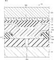
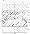
- FIG. 2 is a cross-sectional view showing an example of the configuration of the display device according to the embodiment of the present disclosure.
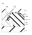
- FIG. 3 is an enlarged cross-sectional view of the region R of FIG.
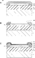
- FIG. 4 is an energy diagram of each layer included in the cross section along the IV-IV line of FIG. 5A, 5B, and 5C are cross-sectional views for explaining an example of a method for manufacturing a display device according to an embodiment of the present disclosure, respectively.
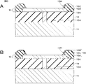
- 6A and 6B are cross-sectional views for explaining an example of a method for manufacturing a display device according to an embodiment of the present disclosure, respectively.
- FIG. 1 is a schematic view showing an example of the overall configuration of the display device according to the embodiment of the present disclosure.
- FIG. 2 is a cross-sectional view showing an example of the configuration of the display device according to the embodiment of the present disclosure.
- FIG. 3 is an
- FIG. 7 is a cross-sectional view showing the configuration of the display device according to Comparative Example 1.
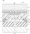
- FIG. 8 is a cross-sectional view showing the configuration of the display device according to Comparative Example 2.
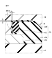
- FIG. 9 is a cross-sectional view showing an example of the configuration of the display device according to the first modification of the embodiment of the present disclosure.
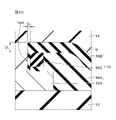
- FIG. 10 is a cross-sectional view showing an example of the configuration of the display device according to the first modification of the embodiment of the present disclosure.
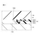
- FIG. 11 is a cross-sectional view showing an example of the configuration of the display device according to the second modification of the embodiment of the present disclosure.
- FIG. 12 is a plan view showing an example of the schematic configuration of the module.
- FIG. 13A is a front view showing an example of the appearance of a digital still camera.
- FIG. 13B is a rear view showing an example of the appearance of the digital still camera.
- FIG. 14 is a perspective view showing an example of the appearance of the head-mounted display.
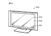
- FIG. 15
- FIG. 1 is a schematic view showing an example of the overall configuration of the display device 10 according to the embodiment of the present disclosure.
- the display device 10 has a display area 110A and a peripheral area 110B provided on the peripheral edge of the display area 110A.
- a plurality of sub-pixels 100R, 100G, and 100B are two-dimensionally arranged in a predetermined arrangement pattern such as a matrix.
- the sub-pixel 100R displays red
- the sub-pixel 100G displays green
- the sub-pixel 100B displays blue.
- the sub-pixels 100R, 100G, and 100B are not particularly distinguished, they are referred to as sub-pixel 100.
- a combination of adjacent sub-pixels 100R, 100G, and 100B constitutes one pixel.
- FIG. 1 shows an example in which a combination of three sub-pixels 100R, 100G, and 100B arranged in the row direction (horizontal direction) constitutes one pixel.
- the peripheral region 110B is provided with a signal line drive circuit 111 and a scanning line drive circuit 112, which are drivers for displaying images.
- the signal line drive circuit 111 supplies the signal voltage of the video signal corresponding to the luminance information supplied from the signal supply source (not shown) to the sub-pixel 100 selected via the signal line 111A.
- the scanning line drive circuit 112 is configured by a shift register or the like that sequentially shifts (transfers) the start pulse in synchronization with the input clock pulse.
- the scanning line drive circuit 112 scans the video signals in line units when writing the video signals to the sub-pixels 100, and sequentially supplies the scanning signals to the scanning lines 112A.
- the display device 10 may be a micro display.
- the display device 10 may be provided in a VR (Virtual Reality) device, an MR (Mixed Reality) device, an AR (Augmented Reality) device, an electronic viewfinder (EVF), a small projector, or the like.
- VR Virtual Reality
- MR Magnetic Reality
- AR Augmented Reality
- EVF electronic viewfinder
- FIG. 2 is a cross-sectional view showing an example of the configuration of the display device 10 according to the embodiment of the present disclosure.
- the display device 10 is between the drive substrate 11, the interlayer insulating layer 12, the first electrode layer 13, the organic electroluminescence layer 14 (hereinafter referred to as “EL layer 14”), the second electrode layer 15, and the elements.
- the insulating layer 16, the protective layer 17, the color filter 18, the filled resin layer 19, and the facing substrate 20 are provided.
- the display device 10 is an example of a light emitting device.
- the display device 10 is a top emission type display device.
- the opposite board 20 side of the display device 10 is the top side, and the drive board 11 side of the display device 10 is the bottom side.
- the surface on the top side of the display device 10 is referred to as a first surface, and the surface on the bottom side of the display device 10 is referred to as a second surface.
- the display device 10 includes a plurality of light emitting elements 10A.
- the plurality of light emitting elements 10A are composed of a first electrode layer 13, an EL layer 14, and a second electrode layer 15.
- the light emitting element 10A is a white light emitting element such as a white OLED or a white Micro-OLED (MODEL).
- a colorization method in the display device 10 a method using a white light emitting element and a color filter 18 is used.
- the colorization method is not limited to this, and a method of extracting three-color light (red light, green light, and blue light) by the resonator structure may be used.
- the color purity may be increased by using the color filter 18 and the resonator structure in combination.
- the drive board 11 is a so-called backplane and drives a plurality of light emitting elements 10A.
- a drive circuit for driving a plurality of light emitting elements 10A, a power supply circuit for supplying electric power to the plurality of light emitting elements 10A, and the like are provided.
- the substrate body of the drive substrate 11 may be made of, for example, glass or resin having low permeability of water and oxygen, or may be made of a semiconductor such as a transistor which can be easily formed.
- the substrate body may be a glass substrate, a semiconductor substrate, a resin substrate, or the like.
- the glass substrate includes, for example, high strain point glass, soda glass, borosilicate glass, forsterite, lead glass, quartz glass and the like.
- the semiconductor substrate includes, for example, amorphous silicon, polycrystalline silicon, single crystal silicon, and the like.
- the resin substrate contains, for example, at least one selected from the group consisting of polymethylmethacrylate, polyvinyl alcohol, polyvinylphenol, polyethersulfone, polyimide, polycarbonate, polyethylene terephthalate, polyethylene naphthalate and the like.
- the interlayer insulating layer 12 (hereinafter, simply referred to as “insulating layer 12”) is provided on the first surface of the drive substrate 11 and covers the drive circuit, the power supply circuit, and the like.
- the insulating layer 12 includes a plurality of contact plugs 12A. Each contact plug 12A connects the light emitting element 10A and the drive circuit.
- the insulating layer 12 may further include a plurality of wirings (not shown).
- the insulating layer 12 may have a single-layer structure or a laminated structure.
- the insulating layer 12 may be an organic insulating layer, an inorganic insulating layer, or a laminate thereof.
- the organic insulating layer contains, for example, at least one selected from the group consisting of polyimide-based resin, acrylic-based resin, novolak-based resin and the like.
- the inorganic insulating layer contains, for example, at least one selected from the group consisting of silicon oxide (SiO x ), silicon nitride (SiN x ), silicon oxynitride (SiO x N y ) and the like.
- the first electrode layer 13 is provided on the first surface of the insulating layer 12.
- the first electrode layer 13 is an anode.
- holes are injected from the first electrode layer 13 into the EL layer 14.
- the first electrode layer 13 also functions as a reflective layer, and it is preferable that the first electrode layer 13 is made of a material having as high a reflectance as possible and a large work function in order to increase the luminous efficiency.
- the first electrode layer 13 has a plurality of electrodes 13A.
- the plurality of electrodes 13A are electrically separated from each other between adjacent light emitting elements 10A.
- the plurality of electrodes 13A share the EL layer 14.
- the plurality of electrodes 13A are two-dimensionally arranged in a predetermined arrangement pattern such as a matrix. Each of the plurality of electrodes 13A is connected to each contact plug 12A provided in the insulating layer 12. The first electrode layer 13 is connected to a drive circuit or wiring via the contact plug 12A.
- the electrode 13A is composed of at least one of a metal layer and a metal oxide layer. More specifically, the electrode 13A is composed of a single-layer film of a metal layer or a metal oxide layer, or a laminated film of a metal layer and a metal oxide layer. When the electrode 13A is composed of a laminated film, the metal oxide layer may be provided on the EL layer 14 side, or the metal layer may be provided on the EL layer 14 side, but it has a high work function. From the viewpoint of placing the layer adjacent to the EL layer 14, it is preferable that the metal oxide layer is provided on the EL layer 14 side.
- the metal layer is, for example, chromium (Cr), gold (Au), platinum (Pt), nickel (Ni), copper (Cu), molybdenum (Mo), titanium (Ti), tantalum (Ta), aluminum (Al). , Magnesium (Mg), Iron (Fe), Tungsten (W) and Silver (Ag).
- the metal layer may contain at least one of the above metal elements as a constituent element of the alloy.
- alloys include aluminum alloys and silver alloys.
- Specific examples of the aluminum alloy include, for example, AlNd or AlCu.
- the metal oxide layer contains, for example, a transparent conductive oxide (TCO: Transparent Conductive Oxide).
- TCO Transparent Conductive Oxide
- the transparent conductive oxide is, for example, a transparent conductive oxide containing indium (hereinafter referred to as "indium-based transparent conductive oxide”) and a transparent conductive oxide containing tin (hereinafter referred to as “tin-based transparent conductive oxide”). ”) And a transparent conductive oxide containing zinc (hereinafter referred to as“ zinc-based transparent conductive oxide ”).
- the indium-based transparent conductive oxide includes, for example, indium tin oxide (ITO), indium zinc oxide (IZO), indium gallium oxide (IGO) or indium gallium zinc oxide (IGZO) fluorine-doped indium oxide (IFO).
- ITO indium tin oxide
- ITO indium tin oxide
- Tin-based transparent conductive oxides include, for example, tin oxide, antimony-doped tin oxide (ATO) or fluorine-doped tin oxide (FTO).
- Zinc-based transparent conductive oxides include, for example, zinc oxide, aluminum-doped zinc oxide (AZO), boron-doped zinc oxide or gallium-doped zinc oxide (GZO).
- the second electrode layer 15 is provided so as to face the first electrode layer 13.
- the second electrode layer 15 is provided as an electrode common to all sub-pixels 100 in the display area 110A.
- the second electrode layer 15 is a cathode.
- the second electrode layer 15 is a transparent electrode having transparency to the light generated by the EL layer 14.
- the transparent electrode also includes a translucent reflective layer.
- the second electrode layer 15 is made of a material having as high a transparency as possible and a small work function in order to increase the luminous efficiency.
- the second electrode layer 15 is composed of, for example, at least one of a metal layer and a metal oxide layer. More specifically, the second electrode layer 15 is composed of a single layer film of a metal layer or a metal oxide layer, or a laminated film of a metal layer and a metal oxide layer. When the second electrode layer 15 is composed of a laminated film, the metal layer may be provided on the EL layer 14 side or the metal oxide layer may be provided on the EL layer 14 side, but the work is low. From the viewpoint of making the layer having a function adjacent to the EL layer 14, it is preferable that the metal layer is provided on the EL layer 14 side.
- the metal layer contains, for example, at least one metal element selected from the group consisting of magnesium (Mg), aluminum (Al), silver (Ag), calcium (Ca) and sodium (Na).
- the metal layer may contain at least one of the above metal elements as a constituent element of the alloy. Specific examples of the alloy include MgAg alloy, MgAl alloy, AlLi alloy and the like.
- the metal oxide layer contains a transparent conductive oxide. As the transparent conductive oxide, the same material as the transparent conductive oxide of the above-mentioned electrode 13A can be exemplified.
- the EL layer 14 is provided between the first electrode layer 13 and the second electrode layer 15.
- the EL layer 14 is continuously provided over all the electrodes 13A in the display area 110A, and is shared by all the electrodes 13A in the display area 110A.
- the EL layer 14 is provided as an organic layer common to all sub-pixels 100 in the display area 110A.
- the EL layer 14 is configured to be capable of emitting white light.
- the EL layer 14 may be an organic EL layer having a 1-stack structure, an organic EL layer having a 2-stack structure, or an organic EL layer other than these.
- the organic EL layer having a 1-stack structure is, for example, from the first electrode layer 13 to the second electrode layer 15, a hole injection layer, a hole transport layer, a red light emitting layer, a light emitting separation layer, a blue light emitting layer, and green.
- the light emitting layer, the electron transport layer, and the electron injection layer are laminated in this order.
- the organic EL layer having a 2-stack structure includes, for example, a hole injection layer, a hole transport layer, a blue light emitting layer, an electron transport layer, a charge generation layer, and a positive electrode layer from the first electrode layer 13 to the second electrode layer 15. It has a structure in which a hole transport layer, a yellow light emitting layer, an electron transport layer, and an electron injection layer are laminated in this order.
- the hole injection layer is for increasing the hole injection efficiency into each light emitting layer and suppressing leakage.
- the hole transport layer is for increasing the hole transport efficiency to each light emitting layer.
- the electron injection layer is for increasing the electron injection efficiency into each light emitting layer.
- the electron transport layer is for increasing the electron transport efficiency to each light emitting layer.
- the light emitting separation layer is a layer for adjusting the injection of carriers into each light emitting layer, and the light emitting balance of each color is adjusted by injecting electrons or holes into each light emitting layer through the light emitting separating layer.
- the charge generation layer supplies electrons and holes to the two light emitting layers sandwiching the charge generation layer, respectively.
- FIG. 3 is an enlarged cross-sectional view of the region R of FIG.
- FIG. 4 is an energy diagram of each layer included in the cross section along the IV-IV line of FIG.
- the inter-element insulating layer 16 (hereinafter, simply referred to as “insulating layer 16”) is provided on the first surface of the insulating layer 12 and between the adjacent first electrode layers 13, and is provided on the adjacent electrodes 13A. Electrically separate between.
- the insulating layer 16 has a plurality of openings 16H. Each of the plurality of openings 16H is provided corresponding to each sub-pixel 100. Each of the plurality of openings 16H is provided on the first surface of each electrode 13A (that is, the surface facing the second electrode layer 15) to expose the first surface of each electrode 13A. The first electrode layer 13 and the EL layer 14 come into contact with each other through the opening 16H.
- the peripheral surface of the opening 16H may be a slope inclined with respect to the first surface of the electrode 13A.
- One opening 16H may be provided for one electrode 13A, or two or more openings 16H may be provided for one electrode 13A.
- the insulating layer 16 covers from the peripheral edge of the first surface of the electrode 13A to the side surface (end surface) of the electrode 13A.
- the peripheral edge portion of the first surface means a region having a predetermined width from the peripheral edge of the first surface toward the inside.
- the insulating layer 16 includes an insulating layer main body 16A, a barrier layer 16B, and a plurality of localized portions 16C.
- the insulating layer 16 forms a potential barrier between the EL layer 14 and the localized portion 16C.
- the carrier is an electron
- the potential barrier formed between the EL layer 14 and the localized portion 16C carriers are localized from the EL layer 14 when a voltage is applied between the first electrode layer 13 and the second electrode layer 15.
- the portion 16C is configured to be tunnelable.
- the insulating layer 16 preferably has a potential barrier formed around the localized portion 16C. That is, it is preferable that the localized portion 16C forms a well-shaped potential in the insulating layer 16. In this case, it is possible to prevent the carrier trapped in the localized portion 16C from being detrapped from the localized portion 16C to surrounding members such as the EL layer 14 and the electrode 13A.
- the barrier layer 16B is provided between the insulating layer main body 16A and the EL layer 14, and between the localized portion 16C and the EL layer 14.
- the barrier layer 16B forms a potential barrier between the EL layer 14 and the localized portion 16C.
- the lower limit of the height of the potential barrier with respect to the localized portion 16C (that is, the energy barrier difference between the localized portion 16C and the barrier layer 16B) is preferably 1 eV or more.
- the upper limit of the height of the potential barrier with respect to the localized portion 16C (that is, the energy barrier difference between the localized portion 16C and the barrier layer 16B) is, for example, 5 eV or less.
- the height of the potential barrier with respect to the EL layer 14 (that is, the energy barrier difference between the EL layer 14 and the barrier layer 16B) is preferably 1 eV or less.
- the height of the potential barrier with respect to the localized portion 16C is 1 eV or more, it is possible to suppress the carriers trapped in the localized portion 16C from being detrapped from the localized portion 16C to the EL layer 14.
- the height of the potential barrier with respect to the EL layer 14 is 1 eV or less, it is possible to suppress a decrease in the number of carriers trapped from the EL layer 14 to the localized portion 16C via the potential barrier.
- the height of the potential barrier with respect to the localized portion 16C and the height of the potential barrier with respect to the EL layer 14 are obtained as follows. It can be obtained by using photoelectron spectroscopy or back-photoelectron spectroscopy for a laminated structure composed of an EL layer 14, an insulating layer main body 16A, a barrier layer 16B, a localized portion 16C, and the like.
- the barrier layer 16B may be made of the same material as the insulating layer main body 16A, or may be made of a material different from that of the insulating layer main body 16A.
- the barrier layer 16B contains, for example, silicon oxide (SiO x ).
- the average thickness of the barrier layer 16B (that is, the average distance between the EL layer 14 and the localized portion 16C) is preferably 2 nm or more and 5 nm or less.
- the average thickness of the barrier layer 16B is 2 nm or more, it is possible to prevent the carriers trapped in the localized portion 16C from being detrapped from the localized portion 16C to the EL layer 14.
- the average thickness of the barrier layer 16B is 5 nm or less, it is possible to suppress a decrease in the number of carriers trapped from the EL layer 14 to the localized portion 16C via the potential barrier.
- the average thickness of the barrier layer 16B (that is, the average distance between the EL layer 14 and the localized portion 16C) is obtained as follows. First, a cross section of the display device 10 (a cross section parallel to the thickness direction of the display device 10) is cut out by cryoFIB (Focused Ion Beam) processing or the like to produce flakes. Subsequently, the prepared flakes are observed by TEM (Transmission Electron Microscope), and one cross-sectional TEM image is acquired. At this time, the acceleration voltage is set to 80 kV. Next, in the acquired one cross-sectional TEM image, the thickness D (see FIG. 3) of the portion of the barrier layer 16B located between the EL layer 14 and the localized portion 16C is measured at 10 points or more.
- cryoFIB Fluorous Ion Beam
- each measurement position is randomly selected from the portion of the barrier layer 16B located between the EL layer 14 and the localized portion 16C.
- the thickness of the barrier layer 16B measured at 10 points or more is simply averaged (arithmetic mean) to obtain the average thickness of the barrier layer 16B.
- the insulating layer main body 16A preferably forms a potential barrier between the localized portion 16C and the electrode 13A. Since a potential barrier is formed between the localized portion 16C and the electrode 13A, it is possible to prevent carriers from being detrapped from the localized portion 16C to the electrode 13A.
- the lower limit of the height of the potential barrier with respect to the localized portion 16C is preferably 1 eV or more. When the height of the potential barrier is 1 eV or more, it is possible to prevent the carriers trapped in the localized portion 16C from being detrapped from the localized portion 16C to the electrode 13A or the like.
- the upper limit of the height of the potential barrier is not particularly limited, but is, for example, 5 eV or less.
- the barrier layer 16B contains, for example, silicon oxide (SiO x ).
- the energy barrier difference between the localized portion 16C and the insulating layer main body 16A can be obtained in the same manner as the energy barrier difference between the localized portion 16C and the barrier layer 16B.
- the localized portion 16C has a plurality of trap orders for trapping carriers in the forbidden band (band gap).
- the localization unit 16C traps carriers reached from the EL layer 14 via the barrier layer 16B in a plurality of trap orders.
- the LUMO (Lowest Unoccupied Molecular Orbital) of the localized portion 16C may be higher than the LUMO of the EL layer 14.
- Each of the plurality of localized portions 16C is provided on the first surface of each electrode 13A (that is, the surface facing the second electrode layer 15).
- Each of the plurality of localization portions 16C is localized around each opening 16H of the insulating layer 16. Since carrier traps are likely to occur in the portion around the opening 16H of the insulating layer 16, the leakage current can be reduced by providing the localized portion 16C around the opening 16H of the insulating layer 16.
- the localized portion 16C is preferably provided adjacent to the barrier layer 16B.
- the localized portion 16C may have a closed loop shape surrounding the opening 16H of the insulating layer 16, or may be provided discretely and discontinuously so as to surround the opening 16H of the insulating layer 16.
- the localized portion 16C is preferably surrounded by an insulating material (for example, silicon oxide (SiO x )) contained in the insulating layer 16. More specifically, it is preferable that the localized portion 16C is adjacent to the peripheral surface of the opening 16H of the insulating layer 16 via the barrier layer 16B.
- the localized portion 16C is preferably separated from the first surface of the electrode 13A. As a result, it is possible to prevent the carriers trapped in the localized portion 16C from being detrapped from the localized portion 16C to the electrode 13A.
- the shortest distance between the first electrode layer 13 and the localized portion 16C may be equal to or greater than the average thickness of the barrier layer 16B from the viewpoint of suppressing carrier detrap from the localized portion 16C to the electrode 13A. preferable.
- the localized portion 16C contains an insulating material different from that of the barrier layer 16B.
- the localized portion 16C is selected from the group consisting of, for example, silicon nitride (SiN x ), silicon nitride (SiO x N y ), hafnium oxide (HfO x ), aluminum oxide (AlO x ) and tantalum oxide (TaO x ). Includes at least one species.
- the protective layer 17 is provided on the first surface of the second electrode layer 15 and covers a plurality of light emitting elements 10A.
- the protective layer 17 blocks the light emitting element 10A from the outside air and suppresses the infiltration of moisture from the external environment into the light emitting element 10A.
- the protective layer 17 may have a function of suppressing oxidation of the metal layer.
- the protective layer 17 is made of, for example, an inorganic material having low hygroscopicity.
- the inorganic material contains, for example, at least one of silicon oxide (SiO), silicon nitride (SiN), silicon oxide nitride (SiNO), titanium oxide (TIO) and aluminum oxide (AlO).
- the protective layer 17 may have a single-layer structure, but may have a multi-layer structure when the thickness of the protective layer 17 is increased. This is to relieve the internal stress in the protective layer 17.
- the protective layer 17 may be made of a polymer resin.
- the polymer resin contains at least one selected from the group consisting of thermosetting resins, ultraviolet curable resins and the like.
- the color filter 18 is provided on the first surface of the protective layer 17.
- the color filter 18 is, for example, an on-chip color filter (OCCF).
- the color filter 18 includes, for example, a red filter, a green filter, and a blue filter.
- the red filter, the green filter, and the blue filter are each provided facing the light emitting element 10A.
- the red filter and the light emitting element 10A form a sub-pixel 100R
- the green filter and the light emitting element 10A form a sub pixel 100G
- the blue filter and the light emitting element 10A form a sub pixel 100B.
- the white light emitted from each of the light emitting elements 10A in the subpixels 100R, 100G, and 100B passes through the red filter, the green filter, and the blue filter, respectively, so that the red light, the green light, and the blue light are displayed on the display surface, respectively. Is emitted from. Further, a light-shielding layer (not shown) may be provided between the color filters of each color, that is, between the sub-pixels.
- the color filter 18 is not limited to the on-chip color filter, and may be provided on one main surface of the facing substrate 20.
- the filling resin layer 19 is provided between the color filter 18 and the facing substrate 20.
- the filled resin layer 19 has a function as an adhesive layer for adhering the color filter 18 and the facing substrate 20.
- the packed resin layer 19 contains at least one selected from the group consisting of, for example, a thermosetting resin and an ultraviolet curable resin.
- the facing board 20 is provided facing the drive board 11. More specifically, the opposed substrate 20 is provided so that the second surface of the opposed substrate 20 and the first surface of the drive substrate 11 face each other.
- the facing substrate 20 and the filled resin layer 19 seal the light emitting element 10A, the color filter 18, and the like.
- the facing substrate 20 is made of a material such as glass that is transparent to each color light emitted from the color filter 18.
- a drive circuit, a power supply circuit, and the like are formed on the first surface of the substrate body by using, for example, a thin film forming technique, a photolithography technique, and an etching technique. As a result, the drive board 11 is obtained.
- the insulating layer 12 is formed on the first surface of the drive substrate 11 so as to cover the drive circuit, the power supply circuit, and the like. At this time, a plurality of contact plugs 12A, a plurality of wirings, and the like are formed on the insulating layer 12.
- the metal layer and the metal oxide layer are sequentially formed on the first surface of the insulating layer 12 by, for example, a sputtering method, and then the metal layer and the metal oxide layer are patterned by using, for example, photolithography and etching techniques. do. As a result, the first electrode layer 13 having the plurality of electrodes 13A is formed.
- the insulating layer 16D is formed on the first surface of the insulating layer 12 so as to cover the plurality of electrodes 13A.
- recesses 16F are formed in portions of the insulating layer 16D located on the first surface of each electrode 13A, as shown in FIG. 5B. At this time, the formation position of each recess 16F is adjusted so that the recess 16F is located inside the peripheral edge of the first surface of the electrode 13A.
- the insulating layer 16E is formed on the first surface of the insulating layer 16D so as to follow each recess 16F.
- the insulating layer 16E is formed on the first surface of the insulating layer 16D so as to follow each recess 16F.
- an opening 16H is formed on each of the first surfaces of the plurality of electrodes 13A.
- a part of the insulating layer 16E remains on the peripheral surface (slope) of the opening 16H, and the localized portion 16C is formed by this residue.
- the insulating layer 16D and the localized portion 16C are surface-treated to form the barrier layer 16B. As a result, the insulating layer 16 is obtained.
- the hole injection layer, the hole transport layer, the red light emitting layer, the light emitting separation layer, the blue light emitting layer, the green light emitting layer, the electron transport layer, and the electron injection layer are formed on the first surface of the electrode 13A and the electron injection layer.
- the EL layer 14 is formed by laminating in this order on the first surface of the insulating layer 16.
- the second electrode layer 15 is formed on the first surface of the EL layer 14 by, for example, a thin film deposition method or a sputtering method. As a result, a plurality of light emitting elements 10A are formed on the first surface of the insulating layer 12.
- the color filter 18 is formed on the first surface of the protective layer 17 by, for example, photolithography. Form.
- the flattening layer may be formed on both the upper, lower or upper and lower sides of the color filter 18.
- ODF One Drop Fill
- the drive substrate 11 and the facing substrate 20 are formed via the filled resin layer 19. Are pasted together. As a result, the display device 10 is sealed. As a result, the display device 10 shown in FIG. 2 is obtained.
- a plurality of sub-pixels 100 share the EL layer 14.
- the interlayer insulating layer 416 known as the interlayer insulating layer
- carriers flow from the electrode 13A to the interface between the EL layer 14 and the interlayer insulating layer 516 and leak.
- the carrier leaks in this way, abnormal light emission occurs around the opening 16H of the interlayer insulating layer 416.
- Comparative Example 2 In order to suppress the occurrence of the above-mentioned abnormal light emission, as shown in FIG. 8, the present inventors have described Comparative Example 2 in which the interlayer insulating layer 516 having a large trap level (defect order) is provided as the interlayer insulating layer.
- the display device 510 is under consideration.
- As the interlayer insulating layer 516 for example, silicon nitride (SiN x ) formed by plasma CVD or the like is used. By providing the interlayer insulating layer 516 having many trap levels, the interfacial conductivity between the EL layer 14 and the interlayer insulating layer 516 is lowered, and carrier leakage is suppressed.
- the insulating layer 16 includes a localized portion 16C localized around the opening 16H of the insulating layer 16, an EL layer 14, and a station.
- a barrier layer 16B provided between the existing portions 16C is provided.
- the barrier layer 16B forms a potential barrier for carriers between the EL layer 14 and the localized portion 16C.
- the peripheral surface of the opening 16H of the insulating layer 16 is the first electrode 13A. It may be a vertical plane substantially perpendicular to the plane.
- the localized portion 16C may be adjacent to both the peripheral surface of the opening 16H of the insulating layer 16 and the first surface (upper surface) of the insulating layer 16 with the barrier layer 16B interposed therebetween.
- the first surface of the insulating layer 16 is the surface on the top side of the display device 10 as described above, and is also the surface facing the second electrode layer 15.
- the thickness D 1 of the barrier layer 16B on the first surface (upper surface) of the insulating layer 16 and the thickness D 2 of the barrier layer 16B on the peripheral surface of the opening 16H of the insulating layer 16 are substantially the same. It may be constant, or as shown in FIG. 10, the thickness D1 of the barrier layer 16B on the first surface (upper surface) of the insulating layer 16 is the barrier layer 16B on the peripheral surface of the opening 16H of the insulating layer 16. It may be thicker than the thickness D2 of. When the thickness D 1 is thicker than the thickness D 2 , the carriers trapped in the localized portion 16C are transferred from the first surface (upper surface) of the insulating layer 16 to the second electrode layer 15. It is possible to suppress the emission in the direction (upward in FIG. 10).
- the thickness D 1 and the thickness D 2 may be substantially the same, or the thickness D 1 may be thicker than the thickness D 2 .
- the insulating layer 16 covers the peripheral edge of the first surface of the electrode 13A as shown in FIG. 3 has been described, but as shown in FIG. 11, the insulating layer 16 is the electrode. It is not necessary to cover the peripheral edge of the first surface of 13A. That is, the entire first surface of the electrode 13A may be exposed from the insulating layer 16 through the opening 16H.
- the localized portion 16C may face the side surface of the electrode 13A.
- the localized portion 16C may be adjacent to the first surface of the insulating layer 16 with the barrier layer 16B interposed therebetween.
- the first surface (upper surface) of the electrode 13A and the first surface (upper surface) of the barrier layer 16B may be substantially the same height.
- the localized portion 16C is preferably provided within a range of 10 nm from the side surface of the electrode 13A.
- the entire localized portion 16C may be provided in the above range, or a part of the localized portion 16C may be provided in the above range.
- Modification 3 In one embodiment described above, an example in which the insulating layer 16 includes the insulating layer main body 16A and the barrier layer 16B has been described. However, the insulating layer main body 16A and the barrier layer 16B are integrated, and the insulating layer main body 16A and the barrier are integrated. An interface may not be provided between the layer 16B and the layer 16.
- the insulating layer 16 includes a localized portion 16C that traps electrons as a carrier
- the insulating layer 16 traps holes as a carrier instead of the localized portion 16C. It may be provided with a localized portion.
- the insulating layer 16 may include a localized portion that traps holes as a carrier together with the localized portion 16C. In this case, the localized portion 16C may be provided around the opening 16H of the insulating layer 16.
- the localization part that traps holes has a plurality of trap orders for trapping holes.
- the display device 10 can be used for various electronic devices.
- the display device 10 is incorporated in various electronic devices, for example, as a module as shown in FIG. In particular, it is suitable for those that require high resolution such as an electronic viewfinder of a video camera or a single-lens reflex camera or a head-mounted display and are used by enlarging them near the eyes.
- This module has a region 210 exposed on one short side of the drive board 11 without being covered by the facing board 20 or the like, and the wiring of the signal line drive circuit 111 and the scanning line drive circuit 112 is connected to this region 210.
- An external connection terminal (not shown) is formed by extending it.
- a flexible printed circuit board (FPC) 220 for signal input / output may be connected to the external connection terminal.
- FPC flexible printed circuit board
- 13A and 13B show an example of the appearance of the digital still camera 310.
- This digital still camera 310 is a single-lens reflex type with interchangeable lenses, and has an interchangeable shooting lens unit (interchangeable lens) 312 in the center of the front of the camera body (camera body) 311 and on the left side of the front. It has a grip portion 313 for the photographer to grip.
- interchangeable shooting lens unit interchangeable lens
- a monitor 314 is provided at a position shifted to the left from the center of the back of the camera body 311.
- An electronic viewfinder (eyepiece window) 315 is provided on the upper part of the monitor 314. By looking into the electronic viewfinder 315, the photographer can visually recognize the optical image of the subject guided from the photographing lens unit 312 and determine the composition.
- the display device 10 can be used as the electronic viewfinder 315.
- FIG. 14 shows an example of the appearance of the head-mounted display 320.
- the head-mounted display 320 has, for example, ear hooks 322 for being worn on the user's head on both sides of the eyeglass-shaped display unit 321.
- a display device 10 can be used as the display unit 321.
- FIG. 15 shows an example of the appearance of the television device 330.
- the television device 330 has, for example, a video display screen unit 331 including a front panel 332 and a filter glass 333, and the video display screen unit 331 is composed of a display device 10.
- the present disclosure is not limited to the above-mentioned one embodiment and its variants, and various types based on the technical idea of the present disclosure. Can be transformed.
- the insulating layer has a plurality of openings, each of which is provided corresponding to each of the electrodes.
- the insulating layer comprises a plurality of localizations, each of which is localized around each of the openings.
- the insulating layer is a display device that forms a potential barrier between the electroluminescence layer and the localized portion.
- the insulating layer contains an insulating material and contains an insulating material.
- the display device according to (1) wherein the localized portion is surrounded by the insulating material.
- the localized portion contains at least one selected from the group consisting of silicon nitride, silicon oxynitride, hafnium oxide, aluminum oxide and tantalum oxide.
- the insulating layer is Insulation layer body and A barrier layer provided between the insulating layer main body and the electroluminescence layer is provided.
- the localized portion is provided adjacent to the barrier layer and is provided.
- the electrode has a facing surface facing the second electrode layer and has a facing surface.
- the display device according to any one of (5), wherein the localized portion is provided on the facing surface.
- the insulating layer has a facing surface facing the second electrode layer, and the thickness of the barrier layer on the facing surface is thicker than the thickness of the barrier layer on the peripheral surface of the opening (6). ).
- the display device according to any one of (1) to (5), wherein the localized portion faces the side surface of the electrode. (9)
- the height of the potential barrier with respect to the localized portion is 1 eV or more and 5 eV or less.
- the display device according to any one of (1) to (8), wherein the height of the potential barrier with respect to the electroluminescence layer is 1 eV or less. (10) The display device according to any one of (1) to (9), wherein the average distance between the electroluminescence layer and the localized portion is 2 nm or more and 5 nm or less. (11) The display device according to any one of (1) to (10), wherein the electroluminescence layer is continuously provided over the plurality of electrodes. (12) The display device according to any one of (1) to (11), wherein the localized portion has a trap order for trapping carriers. (13) The display device according to (12), wherein the carrier is an electron. (14) An electronic device provided with the display device according to any one of (1) to (13).
- Display device 10 Light emitting element 11 Drive board 12 Interlayer insulation layer 13 First electrode layer 13A Electrode 14 Organic electroluminescence layer 15 Second electrode layer 16, 416, 516 Inter-element insulation layer 16A Insulation layer body 16B Barrier layer 16C Localization part 16D, 16E Insulation layer 16F Recess 16H Opening 17 Protective layer 18 Color filter 19 Filling resin layer 20 Opposing substrate 100R, 100G, 100B Sub-pixel 110A Display area 110B Peripheral area 111 Signal line drive circuit 111A Signal line 112 Scanning line drive circuit 112A Scanning line 310 Digital still camera (electronic equipment) 320 Head-mounted display (electronic device) 330 Television equipment (electronic equipment)
Landscapes
- Engineering & Computer Science (AREA)
- Microelectronics & Electronic Packaging (AREA)
- Electroluminescent Light Sources (AREA)
Abstract
Description
2次元配置された複数の電極を有する第1の電極層と、
第1の電極層に対向して設けられた第2の電極層と、
第1の電極層と第2の電極層の間に設けられたエレクトロルミネッセンス層と、
隣接する電極の間に設けられた絶縁層と
を備え、
絶縁層は、複数の開口を有し、複数の開口はそれぞれ、各電極に対応して設けられ、
絶縁層は、複数の局在部を備え、複数の局在部はそれぞれ、各開口の周りに局在し、
絶縁層は、ポテンシャルバリアをエレクトロルミネッセンス層と局在部の間に形成する表示装置である。
1 一実施形態(表示装置の例)
2 変形例(表示装置の変形例)
3 応用例(電子機器の例)
[表示装置の構成]
図1は、本開示の一実施形態に係る表示装置10の全体構成の一例を示す概略図である。表示装置10は、表示領域110Aと、表示領域110Aの周縁に設けられた周辺領域110Bとを有している。表示領域110A内には、複数のサブ画素100R、100G、100Bがマトリクス状等の規定の配置パターンで2次元配置されている。
駆動基板11は、いわゆるバックプレーンであり、複数の発光素子10Aを駆動する。駆動基板11の第1の面上には、複数の発光素子10Aを駆動する駆動回路、および複数の発光素子10Aに電力を供給する電源回路等(いずれも図示せず)が設けられている。
層間絶縁層12(以下、単に「絶縁層12」という。)は、駆動基板11の第1の面上に設けられ、駆動回路および電源回路等を覆っている。絶縁層12は、複数のコンタクトプラグ12Aを備える。各コンタクトプラグ12Aは、発光素子10Aと駆動回路とを接続する。絶縁層12は、複数の配線(図示せず)をさらに備えていてもよい。
第1の電極層13は、絶縁層12の第1の面上に設けられている。第1の電極層13は、アノードである。第1の電極層13と第2の電極層15の間に電圧が加えられると、第1の電極層13からEL層14にホールが注入される。第1の電極層13は、反射層としての機能も兼ねており、できるだけ反射率が高く、かつ仕事関数が大きい材料によって構成されることが、発光効率を高める上で好ましい。第1の電極層13は、複数の電極13Aを有する。複数の電極13Aは、隣接する発光素子10A間で電気的に分離されている。複数の電極13Aは、EL層14を共有している。複数の電極13Aは、マトリクス状等の規定の配置パターンで2次元配置されている。複数の電極13Aはそれぞれ、絶縁層12に備えられた各コンタクトプラグ12Aに接続されている。このコンタクトプラグ12Aを介して第1の電極層13は駆動回路または配線に接続されている。
第2の電極層15は、第1の電極層13と対向して設けられている。第2の電極層15は、表示領域110A内においてすべてのサブ画素100に共通の電極として設けられている。第2の電極層15は、カソードである。第1の電極層13と第2の電極層15の間に電圧が加えられると、第2の電極層15からEL層14に電子が注入される。第2の電極層15は、EL層14で発生した光に対して透過性を有する透明電極である。ここで、透明電極には、半透過性反射層も含まれるものとする。第2の電極層15は、できるだけ透過性が高く、かつ仕事関数が小さい材料によって構成されることが、発光効率を高める上で好ましい。
EL層14は、第1の電極層13と第2の電極層15の間に設けられている。EL層14は、表示領域110A内においてすべての電極13Aに亘って連続して設けられ、表示領域110A内においてすべての電極13Aに共用されている。EL層14は、表示領域110A内においてすべてのサブ画素100に共通の有機層として設けられている。EL層14は、白色光を発光可能に構成されている。
図3は、図2の領域Rの拡大断面図である。図4は、図3のIV-IV線に沿った断面に含まれる各層のエネルギーダイアグラムである。素子間絶縁層16(以下、単に「絶縁層16」という。)は、絶縁層12の第1の面上、かつ、隣接する第1の電極層13の間に設けられ、隣接する電極13Aの間を電気的に分離する。
バリア層16Bは、絶縁層本体16AとEL層14の間、および局在部16CとEL層14の間に設けられている。バリア層16Bは、EL層14と局在部16Cとの間にポテンシャルバリアを形成する。局在部16Cに対するポテンシャルバリアの高さ(すなわち局在部16Cとバリア層16Bとのエネルギー障壁差)の下限値は、好ましくは1eV以上である。局在部16Cに対するポテンシャルバリアの高さ(すなわち局在部16Cとバリア層16Bとのエネルギー障壁差)の上限値は、例えば5eV以下である。EL層14に対するポテンシャルバリアの高さ(すなわちEL層14とバリア層16Bとのエネルギー障壁差)は、好ましくは1eV以下である。局在部16Cに対するポテンシャルバリアの高さが1eV以上であると、局在部16Cにトラップされたキャリアが、局在部16CからEL層14にデトラップされることを抑制することができる。EL層14に対するポテンシャルバリアの高さが1eV以下であると、ポテンシャルバリアを介してEL層14から局在部16Cにトラップされるキャリア数の低下を抑制することができる。
絶縁層本体16Aは、局在部16Cと電極13Aとの間にポテンシャルバリアを形成することが好ましい。局在部16Cと電極13Aとの間にポテンシャルバリアが形成されていることで、局在部16Cから電極13Aにキャリアがデトラップされることを抑制することができる。局在部16Cに対するポテンシャルバリアの高さ(すなわち局在部16Cと絶縁層本体16Aとのエネルギー障壁差)の下限値は、好ましくは1eV以上である。ポテンシャルバリアの高さが1eV以上であると、局在部16Cにトラップされたキャリアが、局在部16Cから電極13A等にデトラップされることを抑制することができる。ポテンシャルバリアの高さの上限値は、特に限定されるものではないが、例えば5eV以下である。バリア層16Bは、例えば、酸化ケイ素(SiOx)を含む。局在部16Cと絶縁層本体16Aとのエネルギー障壁差は、局在部16Cとバリア層16Bとのエネルギー障壁差と同様にして求めることができる。
局在部16Cは、禁止帯(バンドギャップ)中に、キャリアをトラップする複数のトラップ順位を有する。局在部16Cは、EL層14からバリア層16Bを介して到達したキャリアを複数のトラップ順位にトラップする。局在部16CのLUMO(Lowest Unoccupied Molecular Orbital)は、EL層14のLUMOよりも高くてもよい。
保護層17は、第2の電極層15の第1の面上に設けられ、複数の発光素子10Aを覆う。保護層17は、発光素子10Aを外気と遮断し、外部環境から発光素子10A内部への水分浸入を抑制する。また、第2の電極層15が金属層により構成されている場合には、保護層17は、この金属層の酸化を抑制する機能を有していてもよい。
カラーフィルタ18は、保護層17の第1の面上に設けられている。カラーフィルタ18は、例えば、オンチップカラーフィルタ(On Chip Color Filter:OCCF)である。カラーフィルタ18は、例えば、赤色フィルタ、緑色フィルタおよび青色フィルタを備える。赤色フィルタ、緑色フィルタ、青色フィルタはそれぞれ、発光素子10Aに対向して設けられている。赤色フィルタと発光素子10Aとによりサブ画素100Rが構成され、緑色フィルタと発光素子10Aとによりサブ画素100Gが構成され、青色フィルタと発光素子10Aとによりサブ画素100Bが構成されている。
充填樹脂層19は、カラーフィルタ18と対向基板20の間に設けられている。充填樹脂層19は、カラーフィルタ18と対向基板20とを接着する接着層としての機能を有している。充填樹脂層19は、例えば、熱硬化型樹脂および紫外線硬化型樹脂等からなる群より選ばれた少なくとも1種を含む。
対向基板20は、駆動基板11に対向して設けられている。より具体的には、対向基板20は、対向基板20の第2の面と駆動基板11の第1の面とが対向するように設けられている。対向基板20および充填樹脂層19は、発光素子10Aおよびカラーフィルタ18等を封止する。対向基板20は、カラーフィルタ18から出射される各色光に対して透明なガラス等の材料により構成される。
以下、図5A~図5C、図6A、図6Bを参照して、本開示の一実施形態に係る表示装置10の製造方法の一例について説明する。
一実施形態に係る表示装置10の作用効果の理解を容易とするために、比較例1、2に係る表示装置410、510の構成と一実施形態に係る表示装置10の構成を比較して、表示装置10の作用効果について説明する。
(変形例1)
上述の一実施形態では、絶縁層16の開口16Hの周面が斜面である例について説明したが、絶縁層16の開口16Hの周面が、図9に示すように、電極13Aの第1の面に対してほぼ垂直な垂直面であっていてもよい。この場合、局在部16Cは、絶縁層16の開口16Hの周面および絶縁層16の第1の面(上面)の両方にバリア層16Bを挟んで隣接していてもよい。絶縁層16の第1の面は、上述のように表示装置10のトップ側となる面であり、第2の電極層15に対向する対向面でもある。
上述の一実施形態では、図3に示すように、絶縁層16が電極13Aの第1の面の周縁部を覆っている例について説明したが、図11に示すように、絶縁層16が電極13Aの第1の面の周縁部を覆っていなくてもよい。すなわち、電極13Aの第1の面の全体が開口16Hを介して絶縁層16から露出していてもよい。局在部16Cは、電極13Aの側面に対向していてもよい。局在部16Cは、絶縁層16の第1の面にバリア層16Bを挟んで隣接していてもよい。電極13Aの第1の面(上面)とバリア層16Bの第1の面(上面)とは、略同一高さであってもよい。局在部16Cは、局在部16Cにトラップされるキャリア数の低下を抑制する観点からすると、電極13Aの側面から10nm以内の範囲に設けられていることが好ましい。この場合、局在部16Cの全体が上記範囲に設けられていてもよいし、局在部16Cの一部が上記範囲に設けられていてもよい。
上述の一実施形態では、絶縁層16が絶縁層本体16Aとバリア層16Bとを備える例について説明したが、絶縁層本体16Aとバリア層16Bとが一体になっており、絶縁層本体16Aとバリア層16Bとの間に界面が設けられていなくてもよい。
上述の一実施形態では、絶縁層16が、キャリアとして電子をトラップする局在部16Cを備える例について説明したが、絶縁層16が、局在部16Cに代えて、キャリアとして正孔をトラップする局在部を備えるようにしてもよい。あるいは、絶縁層16が、局在部16Cと共に、キャリアとして正孔をトラップする局在部を備えるようにしてもよい。この場合、局在部16Cは、絶縁層16の開口16Hの周りに設けられていてもよい。正孔をトラップする局在部は、正孔をトラップする複数のトラップ順位を有する。
上述の一実施形態では、局在部16Cが、絶縁材料を含む例について説明したが、局在部16Cが、金属等の導電材料を含んでいてもよい。
(電子機器)
上述の一実施形態およびその変形例に係る表示装置10は、各種の電子機器に用いることが可能である。表示装置10は、例えば、図12に示したようなモジュールとして、種々の電子機器に組み込まれる。特にビデオカメラや一眼レフカメラの電子ビューファインダまたはヘッドマウント型ディスプレイ等の高解像度が要求され、目の近くで拡大して使用されるものに適する。このモジュールは、駆動基板11の一方の短辺側に、対向基板20等により覆われず露出した領域210を有し、この領域210に、信号線駆動回路111および走査線駆動回路112の配線を延長して外部接続端子(図示せず)が形成されている。この外部接続端子には、信号の入出力のためのフレキシブルプリント配線基板(Flexible Printed Circuit:FPC)220が接続されていてもよい。
図13A、図13Bは、デジタルスチルカメラ310の外観の一例を示す。このデジタルスチルカメラ310は、レンズ交換式一眼レフレックスタイプのものであり、カメラ本体部(カメラボディ)311の正面略中央に交換式の撮影レンズユニット(交換レンズ)312を有し、正面左側に撮影者が把持するためのグリップ部313を有している。
図14は、ヘッドマウントディスプレイ320の外観の一例を示す。ヘッドマウントディスプレイ320は、例えば、眼鏡形の表示部321の両側に、使用者の頭部に装着するための耳掛け部322を有している。表示部321としては、表示装置10を用いることができる。
図15は、テレビジョン装置330の外観の一例を示す。このテレビジョン装置330は、例えば、フロントパネル332およびフィルターガラス333を含む映像表示画面部331を有しており、この映像表示画面部331は、表示装置10により構成されている。
(1)
2次元配置された複数の電極を有する第1の電極層と、
前記第1の電極層に対向して設けられた第2の電極層と、
前記第1の電極層と前記第2の電極層の間に設けられたエレクトロルミネッセンス層と、
隣接する前記電極の間に設けられた絶縁層と
を備え、
前記絶縁層は、複数の開口を有し、前記複数の開口はそれぞれ、各前記電極に対応して設けられ、
前記絶縁層は、複数の局在部を備え、前記複数の局在部はそれぞれ、各前記開口の周りに局在し、
前記絶縁層は、ポテンシャルバリアを前記エレクトロルミネッセンス層と前記局在部の間に形成する表示装置。
(2)
前記絶縁層は、絶縁材料を含み、
前記局在部は、前記絶縁材料に囲まれている(1)に記載の表示装置。
(3)
前記絶縁層は、前記ポテンシャルバリアを前記局在部の周りに形成する(2)に記載の表示装置。
(4)
前記局在部は、窒化ケイ素、酸窒化ケイ素、酸化ハフニウム、酸化アルミニウムおよび酸化タンタルからなる群より選ばれた少なくとも1種を含み、
前記絶縁材料は、酸化ケイ素を含む(2)または(3)に記載の表示装置。
(5)
前記絶縁層は、
絶縁層本体と、
前記絶縁層本体と前記エレクトロルミネッセンス層の間に設けられたバリア層と
を備え、
前記局在部は、前記バリア層に隣接して設けられ、
前記バリア層が、前記ポテンシャルバリアを形成する(1)から(4)のいずれかに記載の表示装置。
(6)
前記電極は、前記第2の電極層と対向する対向面を有し、
前記局在部は、前記対向面上に設けられている(5)のいずれかに記載の表示装置。
(7)
前記絶縁層は、前記第2の電極層に対向する対向面を有し、該対向面における前記バリア層の厚さは、前記開口の周面における前記バリア層の厚さに比べて厚い(6)に記載の表示装置。
(8)
前記局在部は、前記電極の側面に対向する(1)から(5)のいずれかに記載の表示装置。
(9)
前記局在部に対する前記ポテンシャルバリアの高さは、1eV以上5eV以下であり、
前記エレクトロルミネッセンス層に対する前記ポテンシャルバリアの高さは、1eV以下である(1)から(8)のいずれかに記載の表示装置。
(10)
前記エレクトロルミネッセンス層と前記局在部の間の平均距離は、2nm以上5nm以下である(1)から(9)のいずれかに記載の表示装置。
(11)
前記エレクトロルミネッセンス層は、前記複数の電極に亘って連続して設けられている(1)から(10)のいずれかに記載の表示装置。
(12)
前記局在部は、キャリアをトラップするトラップ順位を有する(1)から(11)のいずれかに記載の表示装置。
(13)
前記キャリアは、電子である(12)に記載の表示装置。
(14)
(1)から(13)のいずれかに記載の表示装置を備える電子機器。
10A 発光素子
11 駆動基板
12 層間絶縁層
13 第1の電極層
13A 電極
14 有機エレクトロルミネッセンス層
15 第2の電極層
16、416、516 素子間絶縁層
16A 絶縁層本体
16B バリア層
16C 局在部
16D、16E 絶縁層
16F 凹部
16H 開口
17 保護層
18 カラーフィルタ
19 充填樹脂層
20 対向基板
100R、100G、100B サブ画素
110A 表示領域
110B 周辺領域
111 信号線駆動回路
111A 信号線
112 走査線駆動回路
112A 走査線
310 デジタルスチルカメラ(電子機器)
320 ヘッドマウントディスプレイ(電子機器)
330 テレビジョン装置(電子機器)
Claims (14)
- 2次元配置された複数の電極を有する第1の電極層と、
前記第1の電極層に対向して設けられた第2の電極層と、
前記第1の電極層と前記第2の電極層の間に設けられたエレクトロルミネッセンス層と、
隣接する前記電極の間に設けられた絶縁層と
を備え、
前記絶縁層は、複数の開口を有し、前記複数の開口はそれぞれ、各前記電極に対応して設けられ、
前記絶縁層は、複数の局在部を備え、前記複数の局在部はそれぞれ、各前記開口の周りに局在し、
前記絶縁層は、ポテンシャルバリアを前記エレクトロルミネッセンス層と前記局在部の間に形成する表示装置。 - 前記絶縁層は、絶縁材料を含み、
前記局在部は、前記絶縁材料に囲まれている請求項1に記載の表示装置。 - 前記絶縁層は、前記ポテンシャルバリアを前記局在部の周りに形成する請求項2に記載の表示装置。
- 前記局在部は、窒化ケイ素、酸窒化ケイ素、酸化ハフニウム、酸化アルミニウムおよび酸化タンタルからなる群より選ばれた少なくとも1種を含み、
前記絶縁材料は、酸化ケイ素を含む請求項2に記載の表示装置。 - 前記絶縁層は、
絶縁層本体と、
前記絶縁層本体と前記エレクトロルミネッセンス層の間に設けられたバリア層と
を備え、
前記局在部は、前記バリア層に隣接して設けられ、
前記バリア層が、前記ポテンシャルバリアを形成する請求項1に記載の表示装置。 - 前記電極は、前記第2の電極層と対向する対向面を有し、
前記局在部は、前記対向面上に設けられている請求項5に記載の表示装置。 - 前記絶縁層は、前記第2の電極層に対向する対向面を有し、該対向面における前記バリア層の厚さは、前記開口の周面における前記バリア層の厚さに比べて厚い請求項6に記載の表示装置。
- 前記局在部は、前記電極の側面に対向する請求項1に記載の表示装置。
- 前記局在部に対する前記ポテンシャルバリアの高さは、1eV以上5eV以下であり、
前記エレクトロルミネッセンス層に対する前記ポテンシャルバリアの高さは、1eV以下である請求項1に記載の表示装置。 - 前記エレクトロルミネッセンス層と前記局在部の間の平均距離は、2nm以上5nm以下である請求項1に記載の表示装置。
- 前記エレクトロルミネッセンス層は、前記複数の電極に亘って連続して設けられている請求項1に記載の表示装置。
- 前記局在部は、キャリアをトラップするトラップ順位を有する請求項1に記載の表示装置。
- 前記キャリアは、電子である請求項12に記載の表示装置。
- 請求項1に記載の表示装置を備える電子機器。
Priority Applications (5)
| Application Number | Priority Date | Filing Date | Title |
|---|---|---|---|
| DE112021006031.7T DE112021006031T5 (de) | 2020-11-17 | 2021-11-11 | Anzeigevorrichtung und elektronische vorrichtung |
| US18/036,299 US12557480B2 (en) | 2020-11-17 | 2021-11-11 | Display device and electronic device |
| KR1020237014373A KR20230104609A (ko) | 2020-11-17 | 2021-11-11 | 표시 장치 및 전자 기기 |
| CN202180076033.2A CN116438591A (zh) | 2020-11-17 | 2021-11-11 | 显示装置和电子装置 |
| JP2022563715A JP7713469B2 (ja) | 2020-11-17 | 2021-11-11 | 表示装置および電子機器 |
Applications Claiming Priority (2)
| Application Number | Priority Date | Filing Date | Title |
|---|---|---|---|
| JP2020191270 | 2020-11-17 | ||
| JP2020-191270 | 2020-11-17 |
Publications (1)
| Publication Number | Publication Date |
|---|---|
| WO2022107679A1 true WO2022107679A1 (ja) | 2022-05-27 |
Family
ID=81708067
Family Applications (1)
| Application Number | Title | Priority Date | Filing Date |
|---|---|---|---|
| PCT/JP2021/041563 Ceased WO2022107679A1 (ja) | 2020-11-17 | 2021-11-11 | 表示装置および電子機器 |
Country Status (7)
| Country | Link |
|---|---|
| US (1) | US12557480B2 (ja) |
| JP (1) | JP7713469B2 (ja) |
| KR (1) | KR20230104609A (ja) |
| CN (1) | CN116438591A (ja) |
| DE (1) | DE112021006031T5 (ja) |
| TW (1) | TWI905309B (ja) |
| WO (1) | WO2022107679A1 (ja) |
Citations (5)
| Publication number | Priority date | Publication date | Assignee | Title |
|---|---|---|---|---|
| JP2003187970A (ja) * | 2001-12-18 | 2003-07-04 | Seiko Epson Corp | 表示装置の製造方法、電子機器の製造方法、表示装置および電子機器 |
| JP2003249376A (ja) * | 2001-12-18 | 2003-09-05 | Seiko Epson Corp | 表示装置及び電子機器 |
| JP2015015194A (ja) * | 2013-07-05 | 2015-01-22 | ソニー株式会社 | 表示装置 |
| WO2018147048A1 (ja) * | 2017-02-13 | 2018-08-16 | ソニー株式会社 | 表示装置、電子機器、および表示装置の製造方法 |
| WO2020111202A1 (ja) * | 2018-11-28 | 2020-06-04 | ソニー株式会社 | 表示装置および電子機器 |
Family Cites Families (9)
| Publication number | Priority date | Publication date | Assignee | Title |
|---|---|---|---|---|
| TWI297226B (en) * | 2006-03-08 | 2008-05-21 | Au Optronics Corp | Organic electroluminescence display and manufacturing method thereof |
| JP5574456B2 (ja) * | 2010-08-06 | 2014-08-20 | パナソニック株式会社 | 発光素子とその製造方法、および発光装置 |
| TWI440172B (zh) * | 2010-09-17 | 2014-06-01 | E Ink Holdings Inc | 有機發光顯示裝置及其製造方法 |
| KR20140127688A (ko) * | 2013-04-25 | 2014-11-04 | 삼성디스플레이 주식회사 | 유기 발광 표시 장치 및 이의 제조 방법 |
| JP6136578B2 (ja) | 2013-05-29 | 2017-05-31 | ソニー株式会社 | 表示装置および表示装置の製造方法ならびに電子機器 |
| JP6242121B2 (ja) * | 2013-09-02 | 2017-12-06 | 株式会社ジャパンディスプレイ | 発光素子表示装置及び発光素子表示装置の製造方法 |
| KR20160066650A (ko) * | 2014-12-02 | 2016-06-13 | 삼성디스플레이 주식회사 | 표시 장치의 제조 방법 및 표시 장치 |
| WO2018147050A1 (ja) | 2017-02-13 | 2018-08-16 | ソニー株式会社 | 表示装置、および電子機器 |
| CN107527939B (zh) * | 2017-08-17 | 2020-07-07 | 京东方科技集团股份有限公司 | 像素界定层及其制造方法、显示基板、显示面板 |
-
2021
- 2021-11-10 TW TW110141756A patent/TWI905309B/zh active
- 2021-11-11 CN CN202180076033.2A patent/CN116438591A/zh active Pending
- 2021-11-11 JP JP2022563715A patent/JP7713469B2/ja active Active
- 2021-11-11 WO PCT/JP2021/041563 patent/WO2022107679A1/ja not_active Ceased
- 2021-11-11 US US18/036,299 patent/US12557480B2/en active Active
- 2021-11-11 DE DE112021006031.7T patent/DE112021006031T5/de active Pending
- 2021-11-11 KR KR1020237014373A patent/KR20230104609A/ko active Pending
Patent Citations (5)
| Publication number | Priority date | Publication date | Assignee | Title |
|---|---|---|---|---|
| JP2003187970A (ja) * | 2001-12-18 | 2003-07-04 | Seiko Epson Corp | 表示装置の製造方法、電子機器の製造方法、表示装置および電子機器 |
| JP2003249376A (ja) * | 2001-12-18 | 2003-09-05 | Seiko Epson Corp | 表示装置及び電子機器 |
| JP2015015194A (ja) * | 2013-07-05 | 2015-01-22 | ソニー株式会社 | 表示装置 |
| WO2018147048A1 (ja) * | 2017-02-13 | 2018-08-16 | ソニー株式会社 | 表示装置、電子機器、および表示装置の製造方法 |
| WO2020111202A1 (ja) * | 2018-11-28 | 2020-06-04 | ソニー株式会社 | 表示装置および電子機器 |
Also Published As
| Publication number | Publication date |
|---|---|
| US20230413609A1 (en) | 2023-12-21 |
| CN116438591A (zh) | 2023-07-14 |
| JPWO2022107679A1 (ja) | 2022-05-27 |
| JP7713469B2 (ja) | 2025-07-25 |
| TWI905309B (zh) | 2025-11-21 |
| TW202223862A (zh) | 2022-06-16 |
| US12557480B2 (en) | 2026-02-17 |
| KR20230104609A (ko) | 2023-07-10 |
| DE112021006031T5 (de) | 2023-09-07 |
Similar Documents
| Publication | Publication Date | Title |
|---|---|---|
| CN108269833B (zh) | 有机发光显示装置 | |
| US20210399264A1 (en) | Display device | |
| TWI651703B (zh) | 有機發光顯示裝置 | |
| WO2022034862A1 (ja) | 表示装置、表示装置の製造方法、並びに、表示装置を用いた電子機器 | |
| KR20210086334A (ko) | 유기 발광 표시 장치 | |
| WO2023095663A1 (ja) | 表示装置および電子機器 | |
| JP7597110B2 (ja) | 表示装置および電子機器 | |
| JP7773999B2 (ja) | 表示装置および電子機器 | |
| JP7750626B2 (ja) | 表示装置、発光装置および電子機器 | |
| JP7713469B2 (ja) | 表示装置および電子機器 | |
| JP7825570B2 (ja) | 表示装置および電子機器 | |
| US12598678B2 (en) | Display device and electronic apparatus | |
| US20230155080A1 (en) | Display device, light-emitting device and electronic apparatus | |
| JP7740808B2 (ja) | 表示装置、発光装置および電子機器 | |
| WO2021246127A1 (ja) | 表示装置および電子機器 | |
| CN114946274A (zh) | 显示装置和显示装置的制造方法以及电子设备 | |
| JP7847154B2 (ja) | 表示装置およびその製造方法、ならびに電子機器 | |
| US20250241134A1 (en) | Display Device and Head-Mounted Display Apparatus | |
| US20260047302A1 (en) | Light emitting device and electronic apparatus | |
| JP7744092B2 (ja) | 表示装置および電子機器 | |
| US20240040844A1 (en) | Display device and electronic device | |
| JP2025536882A (ja) | 表示装置およびその製造方法 |
Legal Events
| Date | Code | Title | Description |
|---|---|---|---|
| 121 | Ep: the epo has been informed by wipo that ep was designated in this application |
Ref document number: 21894553 Country of ref document: EP Kind code of ref document: A1 |
|
| ENP | Entry into the national phase |
Ref document number: 2022563715 Country of ref document: JP Kind code of ref document: A |
|
| WWE | Wipo information: entry into national phase |
Ref document number: 112021006031 Country of ref document: DE |
|
| 122 | Ep: pct application non-entry in european phase |
Ref document number: 21894553 Country of ref document: EP Kind code of ref document: A1 |