WO2022107454A1 - 半導体装置 - Google Patents
半導体装置 Download PDFInfo
- Publication number
- WO2022107454A1 WO2022107454A1 PCT/JP2021/035810 JP2021035810W WO2022107454A1 WO 2022107454 A1 WO2022107454 A1 WO 2022107454A1 JP 2021035810 W JP2021035810 W JP 2021035810W WO 2022107454 A1 WO2022107454 A1 WO 2022107454A1
- Authority
- WO
- WIPO (PCT)
- Prior art keywords
- wiring
- opening
- light emitting
- semiconductor device
- substrate
- Prior art date
- Legal status (The legal status is an assumption and is not a legal conclusion. Google has not performed a legal analysis and makes no representation as to the accuracy of the status listed.)
- Ceased
Links
Images





Classifications
-
- H—ELECTRICITY
- H01—ELECTRIC ELEMENTS
- H01S—DEVICES USING THE PROCESS OF LIGHT AMPLIFICATION BY STIMULATED EMISSION OF RADIATION [LASER] TO AMPLIFY OR GENERATE LIGHT; DEVICES USING STIMULATED EMISSION OF ELECTROMAGNETIC RADIATION IN WAVE RANGES OTHER THAN OPTICAL
- H01S5/00—Semiconductor lasers
- H01S5/40—Arrangement of two or more semiconductor lasers, not provided for in groups H01S5/02 - H01S5/30
- H01S5/42—Arrays of surface emitting lasers
- H01S5/423—Arrays of surface emitting lasers having a vertical cavity
-
- G—PHYSICS
- G01—MEASURING; TESTING
- G01S—RADIO DIRECTION-FINDING; RADIO NAVIGATION; DETERMINING DISTANCE OR VELOCITY BY USE OF RADIO WAVES; LOCATING OR PRESENCE-DETECTING BY USE OF THE REFLECTION OR RERADIATION OF RADIO WAVES; ANALOGOUS ARRANGEMENTS USING OTHER WAVES
- G01S17/00—Systems using the reflection or reradiation of electromagnetic waves other than radio waves, e.g. lidar systems
- G01S17/88—Lidar systems specially adapted for specific applications
- G01S17/89—Lidar systems specially adapted for specific applications for mapping or imaging
- G01S17/894—Three-dimensional [3D] imaging with simultaneous measurement of time-of-flight at a two-dimensional [2D] array of receiver pixels, e.g. time-of-flight cameras or flash lidar
-
- G—PHYSICS
- G01—MEASURING; TESTING
- G01S—RADIO DIRECTION-FINDING; RADIO NAVIGATION; DETERMINING DISTANCE OR VELOCITY BY USE OF RADIO WAVES; LOCATING OR PRESENCE-DETECTING BY USE OF THE REFLECTION OR RERADIATION OF RADIO WAVES; ANALOGOUS ARRANGEMENTS USING OTHER WAVES
- G01S7/00—Details of systems according to groups G01S13/00, G01S15/00, G01S17/00
- G01S7/48—Details of systems according to groups G01S13/00, G01S15/00, G01S17/00 of systems according to group G01S17/00
- G01S7/481—Constructional features, e.g. arrangements of optical elements
- G01S7/4814—Constructional features, e.g. arrangements of optical elements of transmitters alone
- G01S7/4815—Constructional features, e.g. arrangements of optical elements of transmitters alone using multiple transmitters
-
- G—PHYSICS
- G01—MEASURING; TESTING
- G01S—RADIO DIRECTION-FINDING; RADIO NAVIGATION; DETERMINING DISTANCE OR VELOCITY BY USE OF RADIO WAVES; LOCATING OR PRESENCE-DETECTING BY USE OF THE REFLECTION OR RERADIATION OF RADIO WAVES; ANALOGOUS ARRANGEMENTS USING OTHER WAVES
- G01S7/00—Details of systems according to groups G01S13/00, G01S15/00, G01S17/00
- G01S7/48—Details of systems according to groups G01S13/00, G01S15/00, G01S17/00 of systems according to group G01S17/00
- G01S7/483—Details of pulse systems
- G01S7/484—Transmitters
-
- H—ELECTRICITY
- H01—ELECTRIC ELEMENTS
- H01S—DEVICES USING THE PROCESS OF LIGHT AMPLIFICATION BY STIMULATED EMISSION OF RADIATION [LASER] TO AMPLIFY OR GENERATE LIGHT; DEVICES USING STIMULATED EMISSION OF ELECTROMAGNETIC RADIATION IN WAVE RANGES OTHER THAN OPTICAL
- H01S5/00—Semiconductor lasers
- H01S5/02—Structural details or components not essential to laser action
- H01S5/022—Mountings; Housings
- H01S5/023—Mount members, e.g. sub-mount members
- H01S5/02315—Support members, e.g. bases or carriers
-
- H—ELECTRICITY
- H01—ELECTRIC ELEMENTS
- H01S—DEVICES USING THE PROCESS OF LIGHT AMPLIFICATION BY STIMULATED EMISSION OF RADIATION [LASER] TO AMPLIFY OR GENERATE LIGHT; DEVICES USING STIMULATED EMISSION OF ELECTROMAGNETIC RADIATION IN WAVE RANGES OTHER THAN OPTICAL
- H01S5/00—Semiconductor lasers
- H01S5/02—Structural details or components not essential to laser action
- H01S5/022—Mountings; Housings
- H01S5/0233—Mounting configuration of laser chips
- H01S5/0234—Up-side down mountings, e.g. Flip-chip, epi-side down mountings or junction down mountings
-
- H—ELECTRICITY
- H01—ELECTRIC ELEMENTS
- H01S—DEVICES USING THE PROCESS OF LIGHT AMPLIFICATION BY STIMULATED EMISSION OF RADIATION [LASER] TO AMPLIFY OR GENERATE LIGHT; DEVICES USING STIMULATED EMISSION OF ELECTROMAGNETIC RADIATION IN WAVE RANGES OTHER THAN OPTICAL
- H01S5/00—Semiconductor lasers
- H01S5/02—Structural details or components not essential to laser action
- H01S5/022—Mountings; Housings
- H01S5/0239—Combinations of electrical or optical elements
-
- H—ELECTRICITY
- H01—ELECTRIC ELEMENTS
- H01S—DEVICES USING THE PROCESS OF LIGHT AMPLIFICATION BY STIMULATED EMISSION OF RADIATION [LASER] TO AMPLIFY OR GENERATE LIGHT; DEVICES USING STIMULATED EMISSION OF ELECTROMAGNETIC RADIATION IN WAVE RANGES OTHER THAN OPTICAL
- H01S5/00—Semiconductor lasers
- H01S5/40—Arrangement of two or more semiconductor lasers, not provided for in groups H01S5/02 - H01S5/30
- H01S5/4018—Lasers electrically in series
-
- H—ELECTRICITY
- H01—ELECTRIC ELEMENTS
- H01S—DEVICES USING THE PROCESS OF LIGHT AMPLIFICATION BY STIMULATED EMISSION OF RADIATION [LASER] TO AMPLIFY OR GENERATE LIGHT; DEVICES USING STIMULATED EMISSION OF ELECTROMAGNETIC RADIATION IN WAVE RANGES OTHER THAN OPTICAL
- H01S5/00—Semiconductor lasers
- H01S5/02—Structural details or components not essential to laser action
- H01S5/0206—Substrates, e.g. growth, shape, material, removal or bonding
- H01S5/021—Silicon based substrates
-
- H—ELECTRICITY
- H01—ELECTRIC ELEMENTS
- H01S—DEVICES USING THE PROCESS OF LIGHT AMPLIFICATION BY STIMULATED EMISSION OF RADIATION [LASER] TO AMPLIFY OR GENERATE LIGHT; DEVICES USING STIMULATED EMISSION OF ELECTROMAGNETIC RADIATION IN WAVE RANGES OTHER THAN OPTICAL
- H01S5/00—Semiconductor lasers
- H01S5/02—Structural details or components not essential to laser action
- H01S5/022—Mountings; Housings
- H01S5/0233—Mounting configuration of laser chips
- H01S5/02345—Wire-bonding
-
- H—ELECTRICITY
- H01—ELECTRIC ELEMENTS
- H01S—DEVICES USING THE PROCESS OF LIGHT AMPLIFICATION BY STIMULATED EMISSION OF RADIATION [LASER] TO AMPLIFY OR GENERATE LIGHT; DEVICES USING STIMULATED EMISSION OF ELECTROMAGNETIC RADIATION IN WAVE RANGES OTHER THAN OPTICAL
- H01S5/00—Semiconductor lasers
- H01S5/04—Processes or apparatus for excitation, e.g. pumping, e.g. by electron beams
- H01S5/042—Electrical excitation ; Circuits therefor
-
- H—ELECTRICITY
- H01—ELECTRIC ELEMENTS
- H01S—DEVICES USING THE PROCESS OF LIGHT AMPLIFICATION BY STIMULATED EMISSION OF RADIATION [LASER] TO AMPLIFY OR GENERATE LIGHT; DEVICES USING STIMULATED EMISSION OF ELECTROMAGNETIC RADIATION IN WAVE RANGES OTHER THAN OPTICAL
- H01S5/00—Semiconductor lasers
- H01S5/10—Construction or shape of the optical resonator, e.g. extended or external cavity, coupled cavities, bent-guide, varying width, thickness or composition of the active region
- H01S5/18—Surface-emitting [SE] lasers, e.g. having both horizontal and vertical cavities
- H01S5/183—Surface-emitting [SE] lasers, e.g. having both horizontal and vertical cavities having only vertical cavities, e.g. vertical cavity surface-emitting lasers [VCSEL]
- H01S5/18305—Surface-emitting [SE] lasers, e.g. having both horizontal and vertical cavities having only vertical cavities, e.g. vertical cavity surface-emitting lasers [VCSEL] with emission through the substrate, i.e. bottom emission
Definitions
- This disclosure relates to semiconductor devices.
- a surface emitting laser such as VCSEL (Vertical Cavity Surface Emitting Laser) is known.
- VCSEL Vertical Cavity Surface Emitting Laser
- a plurality of light emitting elements are provided in a two-dimensional array on the front surface or the back surface of a substrate.
- a semiconductor device such as a light emitting device may be provided with a lower wiring, an insulating film, and an upper wiring in order on the substrate.
- a light emitting device can be provided by forming a plurality of light emitting elements on one substrate, forming a lower wiring, an insulating film, and an upper wiring on another substrate in order, and mounting the former substrate on the latter substrate. May be manufactured.
- the present disclosure provides a semiconductor device capable of easily reducing the parasitic capacitance between wirings.
- the semiconductor device on the first side surface of the present disclosure includes a first substrate, a lower wiring provided on the first substrate, a plurality of upper wirings provided on the lower wiring via an insulating film, and the above.
- a second substrate provided on the upper wiring via a plurality of elements is provided, and the upper wiring includes first and second wirings adjacent to each other in the first direction, and the element on the first wiring.
- the elements on the second wiring are connected in series with each other, and the first opening is provided in the lower wiring, or between the lower wirings in a second direction different from the first direction.
- the second opening is provided in the upper wiring, or is provided so as to be sandwiched between the upper wirings in the second direction.
- the elements on the first wiring may be connected in parallel with each other, and the elements on the second wiring may be connected in parallel with each other. This makes it possible, for example, to connect the elements in series between the first wiring and the second wiring, and to connect the elements in parallel on the first wiring and the second wiring.
- the element may be a light emitting element provided on the second substrate. This makes it possible to easily reduce, for example, the parasitic capacitance between the wirings in the light emitting device.
- the light emitted from the light emitting element may pass through the second substrate from the lower surface to the upper surface of the second substrate and be emitted from the second substrate. This makes it possible to easily reduce, for example, the parasitic capacitance between the wirings in the backside emitting type light emitting device.
- the lower wiring may be used so that a current flows in the first direction
- the upper wiring may be used so that a current flows in the opposite direction of the first direction. .. This makes it possible, for example, to cancel out the magnetic field generated around the upper wiring and the magnetic field generated around the lower wiring.
- an opening extending in the first direction may be provided as the first or second opening.
- a plurality of openings extending in the first direction and adjacent to each other in the second direction may be provided.
- the lower wiring or the upper wiring includes a plurality of first portions extending in the first direction and a plurality of second portions extending in the second direction, and the plurality of openings.
- Each of the portions may be provided between the first portions adjacent to each other in the second direction.
- the width of the upper wiring in the second direction may be the same as the width of the lower wiring in the second direction. This makes it possible, for example, to preferably cancel the magnetic field generated around the upper wiring and the magnetic field generated around the lower wiring.
- the width of the upper wiring in the second direction may be wider than the width of the lower wiring in the second direction. This makes it possible to realize a more suitable structure than, for example, when the width of the upper wiring in the second direction is narrower than the width of the lower wiring in the second direction.
- the width of the upper wiring in the second direction may be 90% to 110% of the width of the lower wiring in the second direction. This makes it possible to obtain almost the same effect as when these widths are the same, for example.
- the first opening is provided in the lower wiring or is provided so as to be sandwiched between the lower wirings in the second direction, and the first.
- the two openings may be provided in the upper wiring or may be provided so as to be sandwiched between the upper wirings in the second direction. This makes it possible to increase the degree of freedom in wiring design, as compared with the case where only one of the first opening and the second opening is provided, for example.
- the first opening is provided at a position facing the upper wiring in the vertical direction
- the second opening is provided at a position facing the lower wiring in the vertical direction. It may be provided. This makes it possible to further reduce the parasitic capacitance between wirings, for example.
- a plurality of openings extending in the first direction are provided as the first opening
- the lower wiring includes the plurality of first portions extending in the first direction.
- Each of the plurality of openings may be provided between the first portions adjacent to each other in the second direction, including the plurality of second portions extending in the second direction.
- a plurality of openings extending in the first direction are provided as the second opening, and each of the plurality of openings is adjacent to each other in the second direction. It may be provided between the upper wirings. This makes it possible to realize, for example, a structure in which a current can easily flow in the opposite direction of the first direction to the upper wiring even if a plurality of openings are provided as the second openings.
- the width of the first or second opening in the second direction may be 1/10 or less of the width of the upper wiring in the second direction. This makes it possible to further reduce the parasitic capacitance between wirings, for example.
- the plurality of first portions may include a first portion having different widths in the second direction. This makes it possible to increase the degree of freedom in wiring design, for example, as compared with the case where all the first portions have the same width in the second direction.
- a plurality of openings arranged in a two-dimensional array may be provided as the first or second opening. This makes it possible, for example, to reduce the parasitic capacitance between wirings by means of a large number of openings.
- first or second opening only one opening is provided in the upper wiring or the lower wiring, or the upper wiring is provided in the second direction. Only one opening may be provided so as to be sandwiched between the spaces or between the lower wirings. This makes it possible, for example, to reduce the parasitic capacitance between the wirings by one opening.
- the first substrate may be a semiconductor substrate containing silicon (Si), and the second substrate may be a semiconductor substrate containing gallium (Ga) and arsenic (As).
- Si silicon
- Ga gallium
- As arsenic
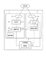
- FIG. 1 is a block diagram showing a configuration of a distance measuring device according to a first embodiment.
- the distance measuring device of FIG. 1 includes a light emitting device 1, an image pickup device 2, and a control device 3.
- the distance measuring device of FIG. 1 irradiates the subject with the light emitted from the light emitting device 1.
- the image pickup apparatus 2 receives the light reflected by the subject and images the subject.
- the control device 3 measures (calculates) the distance to the subject using the image signal output from the image pickup device 2.
- the light emitting device 1 functions as a light source for the image pickup device 2 to take an image of a subject.
- the light emitting device 1 includes a light emitting unit 11, a drive circuit 12, a power supply circuit 13, and a light emitting side optical system 14.
- the image pickup device 2 includes an image sensor 21, an image processing unit 22, and an image pickup side optical system 23.
- the control device 3 includes a ranging unit 31.
- the light emitting unit 11 emits a laser beam for irradiating the subject.
- the light emitting unit 11 of the present embodiment includes a plurality of light emitting elements arranged in a two-dimensional array, and each light emitting element has a VCSEL (Vertical Cavity Surface Emitting Laser) structure. The light emitted from these light emitting elements irradiates the subject.
- the light emitting unit 11 of the present embodiment is provided in a chip called an LD (Laser Diode) chip 41.
- LD Laser Diode
- the drive circuit 12 is an electric circuit that drives the light emitting unit 11.
- the power supply circuit 13 is an electric circuit that generates a power supply voltage of the drive circuit 12. In the distance measuring device of FIG. 1, for example, the power supply circuit 13 generates a power supply voltage from the input voltage supplied from the battery in the distance measuring device, and the drive circuit 12 drives the light emitting unit 11 using this power supply voltage. ..
- the drive circuit 12 of the present embodiment is provided in a substrate called an LDD (Laser Diode Driver) substrate 42.
- LDD Laser Diode Driver
- the light emitting side optical system 14 includes various optical elements, and irradiates the subject with light from the light emitting unit 11 via these optical elements.
- the image pickup side optical system 23 includes various optical elements, and receives light from the subject through these optical elements.
- the image sensor 21 receives light from the subject via the image pickup side optical system 23, and converts this light into an electric signal by photoelectric conversion.
- the image sensor 21 is, for example, a CCD (Charge Coupled Device) sensor or a CMOS (Complementary Metal Oxide Semiconductor) sensor.
- the image sensor 21 of the present embodiment converts the above electronic signal from an analog signal to a digital signal by A / D (Analog to Digital) conversion, and outputs an image signal as a digital signal to the image processing unit 22.
- the image sensor 21 of the present embodiment outputs a frame synchronization signal to the drive circuit 12, and the drive circuit 12 emits light from the light emitting unit 11 at a timing corresponding to the frame cycle of the image sensor 21 based on the frame synchronization signal.
- the image processing unit 22 performs various image processing on the image signal output from the image sensor 21.
- the image processing unit 22 includes, for example, an image processing processor such as a DSP (Digital Signal Processor).
- DSP Digital Signal Processor
- the control device 3 controls various operations of the distance measuring device of FIG. 1, for example, controlling the light emitting operation of the light emitting device 1 and the imaging operation of the image pickup device 2.
- the control device 3 includes, for example, a CPU (Central Processing Unit), a ROM (ReadOnlyMemory), a RAM (RandomAccessMemory), and the like.
- the distance measuring unit 31 measures the distance to the subject based on the image signal output from the image sensor 21 and subjected to image processing by the image processing unit 22.
- the distance measuring unit 31 employs, for example, an STL (Structured Light) method or a ToF (Time of Flight) method as the distance measuring method.
- the distance measuring unit 31 may further measure the distance between the distance measuring device and the subject for each portion of the subject based on the above image signal to specify the three-dimensional shape of the subject.
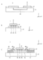
- FIG. 2 is a cross-sectional view showing an example of the structure of the light emitting device 1 of the first embodiment.
- a in FIG. 2 shows a first example of the structure of the light emitting device 1 of the present embodiment.
- the light emitting device 1 of this example includes the above-mentioned LD chip 41 and LDD substrate 42, a mounting substrate 43, and a wiring 44.
- a in FIG. 2 shows an X-axis, a Y-axis, and a Z-axis that are perpendicular to each other.
- the X and Y directions correspond to the horizontal direction (horizontal direction), and the Z direction corresponds to the vertical direction (vertical direction). Further, the + Z direction corresponds to the upward direction, and the ⁇ Z direction corresponds to the downward direction.
- the ⁇ Z direction may or may not exactly coincide with the direction of gravity.
- the X direction is an example of the first direction of the present disclosure
- the Y direction is an example of the second direction of the present disclosure.
- a of FIG. 2 light is emitted from the LD chip 41 in the + Z direction.
- Both the LD chip 41 and the LDD substrate 42 are arranged on the mounting substrate 43.
- the mounting board 43 is, for example, a printed circuit board.
- the image sensor 21 and the image processing unit 22 of FIG. 1 are also arranged on the mounting board 43 of the present embodiment.
- the wiring 44 is provided on the front surface, the back surface, the inside, and the like of the mounting board 43, and electrically connects the LD chip 41 and the LDD board 42.
- the wiring 44 is, for example, a printed wiring provided on the front surface or the back surface of the mounting board 43, or a via wiring penetrating the mounting board 43.
- FIG. 2 shows a second example of the structure of the light emitting device 1 of the present embodiment.
- the light emitting device 1 of this example has the same components as the light emitting device 1 of the first example, but includes a bump 45 instead of the wiring 44.
- the LDD board 42 is arranged on the mounting board 43, and the LD chip 41 is arranged on the LDD board 42.
- the LD chip 41 is arranged on the LDD substrate 42 via the bump 45, and is electrically connected to the LDD substrate 42 by the bump 45.
- the bump 45 is made of, for example, gold (Au).
- FIG. 2 shows a third example of the structure of the light emitting device 1 of the present embodiment.
- the light emitting device 1 of this example includes a circuit board 46, an insulating board 47, a capacitor 48, and a bonding wire 49 in addition to the same components as the light emitting device 1 of the second example.
- the circuit board 46 and the insulating board 47 are arranged on the mounting board 43, the LD chip 41 is arranged on the circuit board 46, and the LDD board 42 and the capacitor 48 are arranged on the insulating board 47. ing. Further, the LD chip 41 is arranged on the circuit board 46 via the bump 45, and is electrically connected to the wiring (not shown) in the circuit board 46 by the bump 45. Further, the LDD substrate 42 and the capacitor 48 are electrically connected to the wiring in the circuit board 46 via the wiring (not shown) in the insulating substrate 47 and the bonding wire 49. Details of the wiring in the circuit board 46 and the wiring in the insulating board 47 will be described later.
- the light emitting device 1 of the present embodiment will be described as having the structure of the third example shown in C of FIG.
- the following description is also applicable to the light emitting device 1 having the structure of the first or second example, except for the description of the structure peculiar to the third example.
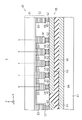
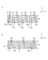
- FIG. 3 is a cross-sectional view showing the structure of the light emitting device 1 of the first embodiment.
- a in FIG. 3 shows an XZ cross section of the light emitting device 1
- B in FIG. 3 shows a YZ cross section of the light emitting device 1.
- FIG. 4 is another cross-sectional view showing the structure of the light emitting device 1 of the first embodiment, and specifically, the XY cross section of FIG. 3A is enlarged and shown.
- the light emitting device 1 is an example of the semiconductor device of the present disclosure.
- the LD chip 41 includes a substrate 51, a laminated film 52, a plurality of light emitting elements 53, a plurality of anode electrodes 54, and a plurality of cathode electrodes 55.
- the circuit board 46 includes a board 61, a plurality of connection pads 62, a plurality of signal wirings 63, a GND (ground) wiring 64, and an insulating film 65.
- the insulating substrate 47 includes a ceramic substrate 71, wiring 72, wiring 73, wiring 74, and wiring 75.
- the substrate 61 and the substrate 51 are examples of the first substrate and the second substrate of the present disclosure, respectively.
- the GND wiring 64 and the signal wiring 63 are examples of the lower wiring and the upper wiring of the present disclosure, respectively.
- the light emitting element 53 is an example of the element of the present disclosure.
- the substrate 51 is a semiconductor substrate such as a GaAs (gallium arsenide) substrate.
- the front surface of the substrate 51 faces the ⁇ Z direction and is the lower surface of the substrate 51
- the back surface of the substrate 51 faces the + Z direction and is the upper surface of the substrate 51.
- the laminated film 52 includes a plurality of layers laminated on the surface (lower surface) of the substrate 51. Examples of these layers are an n-type semiconductor layer, an active layer, a p-type semiconductor layer, a light reflecting layer, an insulating layer provided with a light emission window, and the like.
- the laminated film 52 includes a plurality of mesa portions M protruding in the ⁇ Z direction. A part of these mesas portions M is a plurality of light emitting elements 53.
- the light emitting element 53 is provided on the surface of the substrate 52 as a part of the laminated film 52.
- the light emitting element 53 of the present embodiment has a VCSEL structure and emits light in the + Z direction. As shown in FIG. 4, the light emitted from the light emitting element 53 passes through the inside of the substrate 51 from the front surface (upper surface) of the substrate 51 to the back surface (upper surface), and is emitted from the substrate 51.
- the LD chip 41 of the present embodiment is a back-side emitting type VCSEL chip.
- 3A shows a plurality of light emitting elements 53 included in the light emitting element group D1, a plurality of light emitting elements 53 included in the light emitting element group D2, and a plurality of light emitting elements 53 included in the light emitting element group D3. There is. Details of these light emitting element groups D1 to D3 will be described later.
- the anode electrode 54 is formed on the lower surface of the light emitting element 53.
- the cathode electrode 55 is formed on the lower surface of the mesa portion M other than the light emitting element 53, and extends from the lower surface of the mesa portion M to the lower surface of the laminated film 52 between the mesa portions M.
- Each light emitting element 53 emits light by flowing a current between the corresponding anode electrode 54 and the corresponding cathode electrode 55.
- the substrate 61 is a semiconductor substrate such as a Si (silicon) substrate.
- the front surface of the substrate 61 faces the + Z direction and is the upper surface of the substrate 51
- the back surface of the substrate 61 faces the ⁇ Z direction and is the lower surface of the substrate 51. According to this embodiment, it is possible to provide a circuit on an inexpensive Si substrate (board 61) while providing a light emitting element 53 on a high-performance GaAs substrate (board 51).
- the GND wiring 64, the insulating film 65, the signal wiring 63, and the connection pad 62 are sequentially formed on the substrate 61.
- the GND wiring 64 is formed on the substrate 61 and is used to supply the GND voltage.
- the signal wiring 63 is formed on the GND wiring 64 via the insulating film 65, and is used to supply a signal voltage.
- the GND wiring 64 and the signal wiring 63 are electrically insulated from each other by the insulating film 65.
- the GND wiring 64 and the signal wiring 63 are, for example, Au (gold) wiring.
- the insulating film 65 is, for example, a silicon oxide film.
- the connection pad 62 is formed on the signal wiring 63 and is electrically connected to the signal wiring 63.
- a in FIG. 3 shows an XZ cross section of four signal wirings 63
- B in FIG. 3 shows a YZ cross section of one of these signal wirings 63.
- these signal wirings 63 are adjacent to each other in the X direction.
- the arrow in the signal wiring 63 of FIG. 3A and the reference numeral A1 of B in FIG. 3 indicate the direction of the current flowing in the signal wiring 63.
- the signal wiring 63 of the present embodiment is used so that a current flows in the ⁇ X direction. The details of the shape of the signal wiring 63 will be described later (see B in FIG. 7).
- a in FIG. 3 shows an XZ cross section of one GND wiring 64
- B in FIG. 3 shows a YZ cross section of five parts of the signal wiring 64. As shown in B of FIG. 3, these portions are adjacent to each other in the Y direction.
- the arrow in the GND wiring 64 of FIG. 3A and the reference numeral A2 of B in FIG. 3 indicate the direction of the current flowing in the GND wiring 64.
- the GND wiring 64 of this embodiment is used so that a current flows in the + X direction. The details of the shape of the GND wiring 64 will be described later (see C in FIG. 7).
- the direction of the current flowing in the signal wiring 63 and the direction of the current flowing in the GND wiring 64 are opposite to each other. This makes it possible to cancel the magnetic field generated around the signal wiring 63 and the magnetic field generated around the GND wiring 64.
- the LD chip 41 of this embodiment is mounted on the circuit board 46 via the bump 45.
- the signal wiring 63 is formed on the substrate 61
- the connection pad 62 is formed on the signal wiring 63
- the mesa portion M is arranged on the connection pad 62 via the bump 45.
- the substrate 51 is arranged on the portion M.
- Each mesa portion M is arranged on the bump 45 via the anode electrode 54 or the cathode electrode 55. Therefore, the light emitting element 53 is electrically connected to the signal wiring 63 via the anode electrode 54, the bump 45, and the connection pad 62 (see FIG. 4).
- the insulating substrate 47 includes wirings 72 to 75 on the ceramic substrate 71.
- the LDD board 42 is arranged on the wirings 72 and 73, and is electrically connected to the signal wiring 63 via the wiring 72 and the bonding wire 49, and to the GND wiring 64 via the wiring 73 and the bonding wire 49.
- the capacitor 48 is arranged on the wirings 74 and 75, and is electrically connected to the signal wiring 63 via the wiring 74 and the bonding wire 49, and to the GND wiring 64 via the wiring 75 and the bonding wire 49. There is.
- the LDD substrate 42 of the present embodiment includes a drive circuit 12 that drives the light emitting unit 11.
- the drive circuit 12 in the LDD substrate 42 can drive the light emitting element 53 in the LD chip 41 via the signal wiring 63 or the like.
- FIG. 3A shows a plurality of light emitting elements 53 included in the light emitting element group D1, a plurality of light emitting elements 53 included in the light emitting element group D2, and a plurality of light emitting elements 53 included in the light emitting element group D3.
- these light emitting elements 53 are arranged in a two-dimensional array.
- the light emitting elements 53 of the light emitting element group D1 are provided on the same signal wiring 63, and are connected in parallel between the signal wiring 63 and the signal wiring 63 to the left of the signal wiring 63.
- These signal wirings 63 are examples of the first and second wirings adjacent to each other in the present disclosure. This also applies to the light emitting element groups D2 and D3.
- the light emitting elements 53 of the light emitting element group D2 are provided on one and the same signal wiring 63, and are connected in parallel to each other between the signal wiring 63 and the signal wiring 63 to the left of the signal wiring 63.
- the light emitting elements 53 of the light emitting element group D3 are provided on one and the same signal wiring 63, and are connected in parallel to each other between the signal wiring 63 and the signal wiring 63 to the left of the signal wiring 63.
- the light emitting element 53 of the light emitting element group D1 and the light emitting element 53 of the light emitting element group D2 are connected in series to each other by the signal wiring 63 under the light emitting element group D2.
- the light emitting element 53 of the light emitting element group D2 and the light emitting element 53 of the light emitting element group D3 are connected in series to each other by the signal wiring 63 under the light emitting element group D3.
- the light emitting elements 53 of the same light emitting element group that is, the light emitting elements 53 on the same signal wiring 63 are connected to each other in parallel.
- the light emitting elements 53 of different light emitting element groups that is, the light emitting elements 53 on different signal wirings 63 are connected in series with each other.
- a in FIG. 3 shows the parasitic capacitance C1 generated between the signal wiring 63 and the GND wiring 64 under the light emitting element group D1 and the parasitic capacitance C1 generated between the signal wiring 63 and the GND wiring 64 under the light emitting element group D2.
- the capacitance C2 and the parasitic capacitance C3 generated between the signal wiring 63 and the GND wiring 64 under the light emitting element group D3 are shown.
- FIG. 5 is a cross-sectional view showing the structure of the light emitting device 1 of the first comparative example.
- a in FIG. 5 shows an XZ cross section of the light emitting device 1
- B in FIG. 5 shows a YZ cross section of the light emitting device 1.
- the light emitting device 1 of this comparative example has the same components as the light emitting device 1 of the present embodiment.
- the circuit board 46 of this comparative example includes only one signal wiring 63, and all the mesa portions M of the LD chip 41 of this comparative example are arranged on the signal wiring 63. Therefore, in the light emitting device 1 of this comparative example, all the light emitting elements 53 of the LD chip 41 are connected to each other in parallel.
- the light emitting element 53 of the light emitting element group D1, the light emitting element 53 of the light emitting element group D2, and the light emitting element 53 of the light emitting element group D3 are connected to each other in parallel by the signal wiring 63.
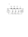
- FIG. 6 is a circuit diagram for explaining the difference between the first embodiment and the first comparative example.
- FIG. 6A shows the circuit configuration of the light emitting device 1 of the first comparative example.
- the light emitting element groups (diodes) D1 to D3 of the LD chip 41 are connected in parallel to each other between the LDD substrate 42 and the capacitor 48.
- FIG. 6B shows the circuit configuration of the light emitting device 1 of the first embodiment.
- the light emitting element groups D1 to D3 of the LD chip 41 are connected in series between the LDD substrate 42 and the capacitor 48.
- the power consumption of the LDD substrate 42 can be reduced as compared with the case where the light emitting element groups D1 to D3 are connected in parallel with each other. It will be possible.
- C in FIG. 6 also shows the circuit configuration of the light emitting device 1 of the first embodiment.
- the parasitic capacitances C1 to C3 as shown in C of FIG. 6 are generated. These parasitic capacitances C1 to C3 delay the signal voltage supplied by the signal wiring 63. This may cause problems such as a decrease in the accuracy of distance measurement by the distance measuring device. Therefore, it is desirable to reduce the parasitic capacitances C1 to C3.
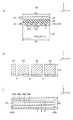
- FIG. 7 is a cross-sectional view and a plan view showing the structure of the circuit board 46 of the first embodiment.
- a in FIG. 7 shows a YZ cross section of the circuit board 46, similar to B in FIG.
- FIG. 7B shows the planar shape of the signal wiring 63.
- FIG. 7C shows the planar shape of the GND wiring 64.
- the circuit board 46 of the present embodiment includes a plurality of signal wirings 63 adjacent to each other in the X direction.
- FIG. 7B shows the width W1 of each signal wiring 63 in the Y direction and a plurality of openings P'provided so as to be sandwiched between the signal wirings 63 in the X direction.
- These openings P' have a linear shape extending in the Y direction, are adjacent to each other in the X direction, and are grooves (slits) sandwiched between the signal wirings 63.
- the circuit board 46 of this embodiment further includes one GND wiring 64 as shown in FIG. 7C.
- FIG. 7C shows the width W2 of the GND wiring 64 in the Y direction and the plurality of openings P provided in the GND wiring 64.
- These openings P have a linear shape extending in the X direction, are adjacent to each other in the Y direction, and are holes that penetrate the GND wiring 64.
- These openings P are examples of the first openings of the present disclosure.
- the GND wiring 64 of the present embodiment includes three or more first portions 64a extending in the X direction and two second portions 64b extending in the Y direction. Each opening P is provided between the first portions 64a adjacent to each other in the Y direction. Further, one second portion 64b is provided at the + X direction end of these first portions 64a, and the other second portion 64b is provided at the ⁇ X direction end of these first portions 64a. ing.
- the opening P in the GND wiring 64 by forming the opening P in the GND wiring 64, it is possible to easily reduce the parasitic capacitances C1 to C3.
- the parasitic capacitances C1 to C3 can be reduced, for example, by forming a cavity in the insulating film 65.
- the step of forming a cavity in the insulating film 65 is difficult to carry out.
- the step of forming the opening P in the GND wiring 64 can be performed by, for example, general photolithography and etching, it can be easily formed. Therefore, according to the present embodiment, it is possible to easily reduce the parasitic capacitances C1 to C3 by forming the opening P in the GND wiring 64.
- the GND wiring 64 of the present embodiment includes the first portion 64a extending in the X direction. Therefore, according to the present embodiment, even if the opening P is formed in the GND wiring 64, a current can flow in the GND wiring 64 in the + X direction.
- the opening P preferably has a shape extending in the X direction, but may not have a shape extending in the X direction as described later.
- a in FIG. 7 shows the width W1 in the Y direction of each signal wiring 63 and the width W2 in the Y direction of the GND wiring 64, similarly to B and C in FIG. A in FIG. 7 further shows the width Wa of each first portion 64a in the Y direction and the width Wb of each opening P in the Y direction.
- the width W1 of each signal wiring is preferably 90% to 110% of the width W2 of the GND wiring (W2 ⁇ 0.9 ⁇ W1 ⁇ W2 ⁇ 1.1). This makes it possible to obtain almost the same effect as when the width W1 and the width W2 are the same.
- the width W1 and the width W2 are different, it is preferable to make the width W1 thicker than the width W2 (W1> W2) rather than making the width W1 thinner than the width W2 (W1 ⁇ W2).
- the width Wa of each first portion 64a and the width Wb of each opening P may be set to arbitrary values.
- the width Wa of all the first portions 64a of the GND wiring 64 is set to the same value
- the width Wb of all the openings P in the GND wiring 64 is set to the same value. ..
- FIG. 8 is a cross-sectional view and a plan view showing the structure of the circuit board 46 of the second comparative example.
- a to C in FIG. 8 correspond to A to C in FIG. 7, respectively.
- the signal wiring 63 of this comparative example has the same shape as the signal wiring 63 of the first embodiment.
- the GND wiring 64 of the first embodiment has the opening P, whereas the GND wiring 64 of this comparative example does not have the opening P. Therefore, in this comparative example, a large parasitic capacitance is generated between the signal wiring 63 and the GND wiring 64.
- d represents the distance between the electrodes
- S represents the area of each electrode
- ⁇ represents the dielectric constant of the material between the electrodes. Therefore, the parasitic capacitance between the signal wiring 63 and the GND wiring 64 can be reduced, for example, by reducing the area of the signal wiring 63 or the area of the GND wiring 64.
- FIG. 9 is a cross-sectional view and a plan view showing the structure of the circuit board 46 of the third comparative example.
- a to C in FIG. 9 correspond to A to C in FIG. 7, respectively.
- the signal wiring 63 and the GND wiring 64 of the present comparative example have substantially the same shape as the signal wiring 63 and the GND wiring 64 of the second comparative example, respectively.
- the width W2 of the GND wiring 64 is narrower than the width W1 of the signal wiring 63.
- the parasitic capacitance of this comparative example is smaller than the parasitic capacitance of the second comparative example. The reason is that the area W2 of the GND wiring 64 becomes narrower, so that the area of the GND wiring 64 becomes smaller.
- FIG. 10 is a circuit diagram for explaining the problem of the third comparative example.
- FIG. 10 shows the circuit configuration of the light emitting device 1 of this comparative example, as in the case of C in FIG.
- the light emitting element groups D1 to D3 of the LD chip 41 are connected in parallel to each other between the LDD substrate 42 and the capacitor 48.
- the parasitic capacitances C1 to C3 can be reduced as compared with the case of the second comparative example.
- the width W2 of the GND wiring 64 is narrowed as in this comparative example, a large parasitic inductance L is generated between the LDD substrate 42 and the light emitting element groups D1 to D3. The reason is that the cancellation between the magnetic field generated around the signal wiring 63 and the magnetic field generated around the GND wiring 64 becomes weak. Such a parasitic inductance L may interfere with the operation of the drive circuit 12 (FIG. 1).
- the width W2 of the GND wiring 64 is set to be the same as the width W1 of the signal wiring 63, and the opening P is provided in the GND wiring 64.
- the parasitic capacitances C1 to C3 of the present embodiment are reduced by reducing the area of the GND wiring 64, as in the case of the second comparative example.
- the parasitic inductance L of the present embodiment is reduced by making the width W2 the same as the width W1 as in the first comparative example. This makes it possible to reduce the parasitic capacitances C1 to C3 and the parasitic inductance L at the same time.
- the circuit board 46 of the present embodiment includes the opening P provided in the GND wiring 64. Therefore, according to the present embodiment, it is possible to easily reduce the parasitic capacitances C1 to C3 between the signal wiring 63 and the GND wiring 64.
- circuit board 46 and the GND wiring 64 of the second to eighth embodiments will be described.
- the second to eighth embodiments are modifications of the first embodiment, and the second to eighth embodiments will be described focusing on the differences from the first embodiment.
- the circuit board 46 and the GND wiring 64 of the second to eighth embodiments are provided in the light emitting device 1 shown in FIG. 3A and the like, similarly to the circuit board 46 and the GND wiring 64 of the first embodiment.
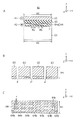
- FIG. 11 is a cross-sectional view and a plan view showing the structure of the circuit board 46 of the second embodiment.
- a to C in FIG. 11 correspond to A to C in FIG. 7, respectively.
- the circuit board 46 of the present embodiment includes a plurality of signal wirings 63 having a shape different from that of the first embodiment, and one GND wiring 64 having the same shape as that of the first embodiment. As shown in B of FIG. 11, these signal wirings 63 are adjacent to each other in the X direction and the Y direction.
- the circuit board 46 of the present embodiment is sandwiched between a plurality of openings P'provided so as to be sandwiched between signal wirings 63 adjacent to each other in the X direction and signal wirings 63 adjacent to each other in the Y direction. It is provided with a plurality of provided openings P.
- the opening P'between the signal wirings 63 extends in the Y direction and is adjacent to each other in the X direction, whereas the opening P between the signal wirings 63 extends in the X direction and extends in the Y direction. Adjacent to each other.
- the opening P between the signal wirings 63 is an example of the second opening of the present disclosure.
- the opening P by forming the opening P between the signal wirings 63, it is possible to easily reduce the parasitic capacitances C1 to C3 as in the case of forming the opening P in the GND wiring 64. It becomes. Further, according to the present embodiment, since the opening P can be formed between the signal wiring 63 and in the GND wiring 64, it is possible to increase the degree of freedom in designing the signal wiring 63 and the GND wiring 64. ..
- each signal wiring 63 of the present embodiment has a shape extending in the X direction
- the GND wiring 64 of the present embodiment has a shape extending in the X direction.
- the opening P preferably has a shape extending in the X direction, but may not have a shape extending in the X direction as described later.
- the opening P in the GND wiring 64 of the present embodiment is provided at a position facing the signal wiring 63 in the Z direction, and is provided between the signal wirings 63 of the present embodiment.
- the opening P is provided at a position facing the GND wiring 64 in the Z direction.
- the openings P in the GND wiring 64 and the openings P between the signal wiring 63 are arranged alternately. This makes it possible to further reduce the parasitic capacitances C1 to C3.
- FIG. 12 is a plan view showing the structures of the signal wiring 63 and the GND wiring 64 of the modified example of the second embodiment.
- a in FIG. 12 shows the signal wiring 63 of the first modification of the present embodiment.
- the opening P is provided in the signal wiring 63.
- each signal wiring 63 of the present modification includes three or more first portions 63a extending in the X direction and two second portions 63b extending in the Y direction, and each opening P. Is provided between the first portions 63a adjacent to each other in the Y direction.
- the opening P in the signal wiring 63 is also an example of the second opening of the present disclosure.
- the signal wiring 63 of this modification may face the GND wiring 64 shown in FIG. 11C, or may face the GND wiring 64 of the second modification described later.
- FIG. 12 shows the GND wiring 64 of the second modification of the present embodiment.
- the opening P is provided in the GND wiring 64 or is provided so as to be sandwiched between the GND wirings 63 in the Y direction.
- Each opening P of the former is surrounded by two first portions 64a and two second portions 64b, and each opening P of the latter has two first portions 64a and one first portion. It is adjacent to the second portion 64b.
- the opening P between the GND wirings 64 is also an example of the first opening of the present disclosure.
- the GND wiring 64 of this modification may face the signal wiring 63 shown in FIG. 11B, or may face the signal wiring 63 of the first modification described above.
- each opening P between the signal wirings 63 shown in FIG. 11B is sandwiched between the two signal wirings 63, and each opening P between the GND wirings 64 shown in FIG. 12B is 1. It is sandwiched between two parts (first part 64a) of the GND wiring 64 of a book. However, each opening P of the former may be sandwiched between two parts of one signal wiring 63, and each opening P of the latter may be sandwiched between two GND wirings 64. May be good.
- the circuit board 46 of the present embodiment includes an opening P provided between the signal wirings 63 in addition to the opening P provided in the GND wiring 64. Therefore, according to the present embodiment, it is possible to further reduce the parasitic capacitances C1 to C3 between the signal wiring 63 and the GND wiring 64, and to increase the degree of design freedom of the signal wiring 63 and the GND wiring 64. ..
- FIG. 13 is a cross-sectional view and a plan view showing the structure of the circuit board 46 of the third embodiment.
- a to C in FIG. 13 correspond to A to C in FIG. 7, respectively.
- the circuit board 46 of the present embodiment includes a plurality of signal wirings 63 having the same shape as that of the first embodiment, and one GND wiring 64 having substantially the same shape as that of the first embodiment.
- the width Wb of the opening P in the GND wiring 64 is set to be 1/10 or less of the width W1 of the signal wiring 63 (Wb ⁇ W1 / 10).
- the width Wb of the present embodiment is set to 1/10 or less of the width W1. This condition may be applied when the opening P is formed between the GND wirings 64, the signal wiring 63, or the signal wiring 63.
- the width W1 of the signal wiring 63 is the same as the width W2 of the GND wiring 64 in this embodiment, it may be different from the width W2 of the GND wiring 64.
- the width W1 may be 90% to 110% of the width W2, or may be thicker than the width W2.
- FIG. 14 is a cross-sectional view and a plan view showing the structure of the circuit board 46 of the fourth embodiment.
- a to C in FIG. 14 correspond to A to C in FIG. 7, respectively.
- the circuit board 46 of the present embodiment includes a plurality of signal wirings 63 having the same shape as that of the first embodiment, and one GND wiring 64 having substantially the same shape as that of the first embodiment.
- the GND wiring 64 of the present embodiment includes the first portion 64a having different widths Wa as the above-mentioned first portion 64a.
- the width Wa of all the first portions 64a does not have to be the same value. This makes it possible to increase the degree of freedom in designing the GND wiring 64 as compared with the case where the width Wa of all the first portions 64a is the same.
- each signal wiring 63 of the second embodiment may also include a first portion 63a having different widths in the Y direction, similarly to the GND wiring 64 of the present embodiment. This makes it possible to increase the degree of freedom in designing each signal wiring 63 as compared with the case where all the first portions 63a have the same width.
- FIG. 15 is a cross-sectional view and a plan view showing the structure of the circuit board 46 of the fifth embodiment.
- a to C in FIG. 15 correspond to A to C in FIG. 7, respectively.
- the circuit board 46 of the present embodiment includes a plurality of signal wirings 63 having a shape different from that of the first embodiment, and one GND wiring 64 having the same shape as that of the first embodiment.
- the GND wiring 64 of the present embodiment includes three or more first portions 64a extending in the X direction and three or more second portions 64b extending in the Y direction. Includes a plurality of openings P arranged in a two-dimensional array. These openings P extend in the X direction and are adjacent to each other in the X and Y directions. According to this embodiment, it is possible to provide a large number of small openings P in the GND wiring 64.
- each signal wiring 63 of the second embodiment may also include a plurality of openings P arranged in a two-dimensional array like the GND wiring 64 of the present embodiment. This makes it possible to provide a large number of small openings P in each signal wiring 63.
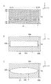
- FIG. 16 is a plan view showing the shape of the GND wiring 64 of the sixth to eighth embodiments.
- the sixth to eighth embodiments correspond to the modified examples of the fifth embodiment.
- a in FIG. 16 shows the shape of the GND wiring 64 of the sixth embodiment.
- the GND wiring 64 of the present embodiment includes a plurality of openings P arranged in a two-dimensional array like the GND wiring 64 of the fifth embodiment.
- each opening P of the present embodiment has a circular planar shape. According to this embodiment, it is possible to provide a large number of small openings P in the GND wiring 64.
- the GND wiring 64 of the present embodiment includes only one opening P.
- the opening P extends in the X direction and has a rectangular planar shape. According to this embodiment, it is possible to provide a large single opening P in the GND wiring 64.
- the GND wiring 64 of the present embodiment also includes only one opening P.
- the opening P extends in the X direction and has an elliptical planar shape. According to this embodiment, it is possible to provide a large single opening P in the GND wiring 64.
- the opening P of the sixth to eighth embodiments may be applied to each signal wiring 63 of the second embodiment. This makes it possible to provide a large number of small openings P in each signal wiring 63 and to provide a single large opening P in each signal wiring 63.
- the light emitting device 1 of the first to eighth embodiments is used as a light source of the distance measuring device, it may be used in other embodiments.
- the light emitting device 1 of these embodiments may be used as a light source of an optical device such as a printer, or may be used as a lighting device.
- the upper wiring includes first and second wiring adjacent to each other in the first direction.
- the element on the first wiring and the element on the second wiring are connected in series with each other.
- the first opening is provided in the lower wiring, or is provided so as to be sandwiched between the lower wirings in a second direction different from the first direction, or the second opening is the said.
- a semiconductor device provided in the upper wiring or sandwiched between the upper wirings in the second direction.
- the lower wiring is used to allow current to flow in the first direction.
- the top wiring is used to allow current to flow in the opposite direction of the first direction.
- the lower wiring or the upper wiring includes a plurality of first portions extending in the first direction and a plurality of second portions extending in the second direction.
- the first opening is provided in the lower wiring, or is provided so as to be sandwiched between the lower wirings in the second direction, and the second opening is in the upper wiring.
- the semiconductor device according to (1) which is provided in the above, or is provided so as to be sandwiched between the upper wirings in the second direction.
- the first opening is provided at a position facing the upper wiring in the vertical direction.
- the second opening is provided at a position facing the lower wiring in the vertical direction.
- the first opening a plurality of openings extending in the first direction are provided.
- the lower wiring includes a plurality of first portions extending in the first direction and a plurality of second portions extending in the second direction.
- each of the plurality of openings is provided between the upper wirings adjacent to each other in the second direction.
- the first substrate is a semiconductor substrate containing silicon (Si), and is a semiconductor substrate.
- the second substrate is a semiconductor substrate containing gallium (Ga) and arsenic (As).
- the light emitting device according to (1) is a semiconductor substrate containing silicon (Si), and is a semiconductor substrate.
- the second substrate is a semiconductor substrate containing gallium (Ga) and arsenic (As).
Landscapes
- Physics & Mathematics (AREA)
- General Physics & Mathematics (AREA)
- Electromagnetism (AREA)
- Condensed Matter Physics & Semiconductors (AREA)
- Optics & Photonics (AREA)
- Engineering & Computer Science (AREA)
- Computer Networks & Wireless Communication (AREA)
- Radar, Positioning & Navigation (AREA)
- Remote Sensing (AREA)
- Semiconductor Lasers (AREA)
- Combinations Of Printed Boards (AREA)
- Internal Circuitry In Semiconductor Integrated Circuit Devices (AREA)
- Semiconductor Integrated Circuits (AREA)
Abstract
Description
図1は、第1実施形態の測距装置の構成を示すブロック図である。
図10は、図6のCと同様に、本比較例の発光装置1の回路構成を示している。本比較例では、LDチップ41の発光素子群D1~D3が、LDD基板42とキャパシタ48との間で互いに並列に接続されている。
図11は、第2実施形態の回路基板46の構造を示す断面図および平面図である。図11のA~Cはそれぞれ、図7のA~Cに対応している。
図13は、第3実施形態の回路基板46の構造を示す断面図および平面図である。図13のA~Cはそれぞれ、図7のA~Cに対応している。
図14は、第4実施形態の回路基板46の構造を示す断面図および平面図である。図14のA~Cはそれぞれ、図7のA~Cに対応している。
図15は、第5実施形態の回路基板46の構造を示す断面図および平面図である。図15のA~Cはそれぞれ、図7のA~Cに対応している。
図16は、第6~第8実施形態のGND配線64の形状を示す平面図である。第6~第8実施形態は、第5実施形態の変形例に相当する。
第1基板と、
前記第1基板上に設けられた下部配線と、
前記下部配線上に絶縁膜を介して設けられた複数の上部配線と、
前記上部配線上に複数の素子を介して設けられた第2基板とを備え、
前記上部配線は、第1方向に互いに隣接する第1および第2配線を含み、
前記第1配線上の前記素子と、前記第2配線上の前記素子は、互いに直列に接続されており、
第1開口部が、前記下部配線内に設けられているか、または前記第1方向と異なる第2方向に前記下部配線間に挟まれるように設けられている、または、第2開口部が、前記上部配線内に設けられているか、または前記第2方向に前記上部配線間に挟まれるように設けられている、半導体装置。
前記第1配線上の前記素子同士は、互いに並列に接続されており、
前記第2配線上の前記素子同士は、互いに並列に接続されている、
(1)に記載の半導体装置。
前記素子は、前記第2基板に設けられた発光素子である、(1)に記載の半導体装置。
前記発光素子から出射された光は、前記第2基板の下面から上面へと前記第2基板内を透過して、前記第2基板から出射される、(3)に記載の発光装置。
前記下部配線は、前記第1方向に電流が流れるように使用され、
前記上部配線は、前記第1方向の逆方向に電流が流れるように使用される、
(1)に記載の半導体装置。
前記第1または第2開口部として、前記第1方向に延びる開口部が設けられている、(1)に記載の半導体装置。
前記第1または第2開口部として、前記第1方向に延び、前記第2方向に互いに隣接する複数の開口部が設けられている、(1)に記載の半導体装置。
前記下部配線または前記上部配線は、前記第1方向に延びる複数の第1部分と、前記第2方向に延びる複数の第2部分とを含み、
前記複数の開口部の各々は、前記第2方向に互いに隣接する前記第1部分間に設けられている、(7)に記載の半導体装置。
前記上部配線の前記第2方向の幅は、前記下部配線の前記第2方向の幅と同じである、(1)に記載の半導体装置。
前記上部配線の前記第2方向の幅は、前記下部配線の前記第2方向の幅より太い、(1)に記載の半導体装置。
前記上部配線の前記第2方向の幅は、前記下部配線の前記第2方向の幅の90%~110%である、(1)に記載の半導体装置。
前記第1開口部が、前記下部配線内に設けられているか、または前記第2方向に前記下部配線間に挟まれるように設けられており、かつ、前記第2開口部が、前記上部配線内に設けられているか、または前記第2方向に前記上部配線間に挟まれるように設けられている、(1)に記載の半導体装置。
前記第1開口部は、前記上部配線と上下方向に対向する位置に設けられており、
前記第2開口部は、前記下部配線と上下方向に対向する位置に設けられている、
(12)に記載の半導体装置。
前記第1開口部として、前記第1方向に延びる複数の開口部が設けられており、
前記下部配線は、前記第1方向に延びる複数の第1部分と、前記第2方向に延びる複数の第2部分とを含み、
前記複数の開口部の各々は、前記第2方向に互いに隣接する前記第1部分間に設けられている、(12)に記載の半導体装置。
前記第2開口部として、前記第1方向に延びる複数の開口部が設けられており、
前記複数の開口部の各々は、前記第2方向に互いに隣接する前記上部配線間に設けられている、(12)に記載の半導体装置。
前記第1または第2開口部の前記第2方向の幅は、前記上部配線の前記第2方向の幅の10分の1以下である、(1)に記載の半導体装置。
前記複数の第1部分は、前記第2方向の幅が互いに異なる第1部分を含む、(8)に記載の半導体装置。
前記第1または第2開口部として、2次元アレイ状に配置された複数の開口部が設けられている、(1)に記載の半導体装置。
前記第1または第2開口部として、前記上部配線内または前記下部配線内に開口部が1つだけ設けられているか、または、前記第2方向に前記上部配線間または前記下部配線間に挟まれるように開口部が1つだけ設けられている、(1)に記載の半導体装置。
前記第1基板は、シリコン(Si)を含む半導体基板であり、
前記第2基板は、ガリウム(Ga)およびヒ素(As)を含む半導体基板である、
(1)に記載の発光装置。
11:発光部、12:駆動回路、13:電源回路、14:発光側光学系、
21:イメージセンサ、22:画像処理部、23:撮像側光学系、31:測距部、
41:LDチップ、42:LDD基板、43:実装基板、
44:配線、45:バンプ、46:回路基板、
47:絶縁基板、48:キャパシタ、49:ボンディングワイヤ、
51:基板、52:積層膜、53:発光素子、
54:アノード電極、55:カソード電極、
61:基板、62:接続パッド、
63:信号配線、63a:第1部分、63b:第2部分、
64:GND配線、64a:第1部分、64b:第2部分、65:絶縁膜、
71:セラミック基板、72:配線、73:配線、74:配線、75:配線
Claims (20)
- 第1基板と、
前記第1基板上に設けられた下部配線と、
前記下部配線上に絶縁膜を介して設けられた複数の上部配線と、
前記上部配線上に複数の素子を介して設けられた第2基板とを備え、
前記上部配線は、第1方向に互いに隣接する第1および第2配線を含み、
前記第1配線上の前記素子と、前記第2配線上の前記素子は、互いに直列に接続されており、
第1開口部が、前記下部配線内に設けられているか、または前記第1方向と異なる第2方向に前記下部配線間に挟まれるように設けられている、または、第2開口部が、前記上部配線内に設けられているか、または前記第2方向に前記上部配線間に挟まれるように設けられている、半導体装置。 - 前記第1配線上の前記素子同士は、互いに並列に接続されており、
前記第2配線上の前記素子同士は、互いに並列に接続されている、
請求項1に記載の半導体装置。 - 前記素子は、前記第2基板に設けられた発光素子である、請求項1に記載の半導体装置。
- 前記発光素子から出射された光は、前記第2基板の下面から上面へと前記第2基板内を透過して、前記第2基板から出射される、請求項3に記載の半導体装置。
- 前記下部配線は、前記第1方向に電流が流れるように使用され、
前記上部配線は、前記第1方向の逆方向に電流が流れるように使用される、
請求項1に記載の半導体装置。 - 前記第1または第2開口部として、前記第1方向に延びる開口部が設けられている、請求項1に記載の半導体装置。
- 前記第1または第2開口部として、前記第1方向に延び、前記第2方向に互いに隣接する複数の開口部が設けられている、請求項1に記載の半導体装置。
- 前記下部配線または前記上部配線は、前記第1方向に延びる複数の第1部分と、前記第2方向に延びる複数の第2部分とを含み、
前記複数の開口部の各々は、前記第2方向に互いに隣接する前記第1部分間に設けられている、請求項7に記載の半導体装置。 - 前記上部配線の前記第2方向の幅は、前記下部配線の前記第2方向の幅と同じである、請求項1に記載の半導体装置。
- 前記上部配線の前記第2方向の幅は、前記下部配線の前記第2方向の幅より太い、請求項1に記載の半導体装置。
- 前記上部配線の前記第2方向の幅は、前記下部配線の前記第2方向の幅の90%~110%である、請求項1に記載の半導体装置。
- 前記第1開口部が、前記下部配線内に設けられているか、または前記第2方向に前記下部配線間に挟まれるように設けられており、かつ、前記第2開口部が、前記上部配線内に設けられているか、または前記第2方向に前記上部配線間に挟まれるように設けられている、請求項1に記載の半導体装置。
- 前記第1開口部は、前記上部配線と上下方向に対向する位置に設けられており、
前記第2開口部は、前記下部配線と上下方向に対向する位置に設けられている、
請求項12に記載の半導体装置。 - 前記第1開口部として、前記第1方向に延びる複数の開口部が設けられており、
前記下部配線は、前記第1方向に延びる複数の第1部分と、前記第2方向に延びる複数の第2部分とを含み、
前記複数の開口部の各々は、前記第2方向に互いに隣接する前記第1部分間に設けられている、請求項12に記載の半導体装置。 - 前記第2開口部として、前記第1方向に延びる複数の開口部が設けられており、
前記複数の開口部の各々は、前記第2方向に互いに隣接する前記上部配線間に設けられている、請求項12に記載の半導体装置。 - 前記第1または第2開口部の前記第2方向の幅は、前記上部配線の前記第2方向の幅の10分の1以下である、請求項1に記載の半導体装置。
- 前記複数の第1部分は、前記第2方向の幅が互いに異なる第1部分を含む、請求項8に記載の半導体装置。
- 前記第1または第2開口部として、2次元アレイ状に配置された複数の開口部が設けられている、請求項1に記載の半導体装置。
- 前記第1または第2開口部として、前記上部配線内または前記下部配線内に開口部が1つだけ設けられているか、または、前記第2方向に前記上部配線間または前記下部配線間に挟まれるように開口部が1つだけ設けられている、請求項1に記載の半導体装置。
- 前記第1基板は、シリコン(Si)を含む半導体基板であり、
前記第2基板は、ガリウム(Ga)およびヒ素(As)を含む半導体基板である、
請求項1に記載の半導体装置。
Priority Applications (3)
| Application Number | Priority Date | Filing Date | Title |
|---|---|---|---|
| DE112021006033.3T DE112021006033T5 (de) | 2020-11-19 | 2021-09-29 | Halbleitervorrichtung |
| CN202180076645.1A CN116508149A (zh) | 2020-11-19 | 2021-09-29 | 半导体装置 |
| US18/030,631 US20230369830A1 (en) | 2020-11-19 | 2021-09-29 | Semiconductor device |
Applications Claiming Priority (2)
| Application Number | Priority Date | Filing Date | Title |
|---|---|---|---|
| JP2020192546A JP2024004500A (ja) | 2020-11-19 | 2020-11-19 | 半導体装置 |
| JP2020-192546 | 2020-11-19 |
Publications (1)
| Publication Number | Publication Date |
|---|---|
| WO2022107454A1 true WO2022107454A1 (ja) | 2022-05-27 |
Family
ID=81708880
Family Applications (1)
| Application Number | Title | Priority Date | Filing Date |
|---|---|---|---|
| PCT/JP2021/035810 Ceased WO2022107454A1 (ja) | 2020-11-19 | 2021-09-29 | 半導体装置 |
Country Status (5)
| Country | Link |
|---|---|
| US (1) | US20230369830A1 (ja) |
| JP (1) | JP2024004500A (ja) |
| CN (1) | CN116508149A (ja) |
| DE (1) | DE112021006033T5 (ja) |
| WO (1) | WO2022107454A1 (ja) |
Citations (3)
| Publication number | Priority date | Publication date | Assignee | Title |
|---|---|---|---|---|
| US20170170799A1 (en) * | 2015-12-11 | 2017-06-15 | Intel Corporation | Capacitive compensation structures using partially meshed ground planes |
| JP2019067805A (ja) * | 2017-09-28 | 2019-04-25 | デンカ株式会社 | 多層回路基板及びその製造方法 |
| JP2020038855A (ja) * | 2018-08-31 | 2020-03-12 | ソニーセミコンダクタソリューションズ株式会社 | 光源装置、調整方法、センシングモジュール |
Family Cites Families (11)
| Publication number | Priority date | Publication date | Assignee | Title |
|---|---|---|---|---|
| JP4216603B2 (ja) | 2001-03-02 | 2009-01-28 | イノベイティブ・ソリューションズ・アンド・サポート・インコーポレイテッド | ヘッドアップディスプレイのためのイメージ表示生成器 |
| JP4956874B2 (ja) | 2001-08-02 | 2012-06-20 | ソニー株式会社 | 半導体装置及び半導体の製造方法 |
| US8675706B2 (en) * | 2011-12-24 | 2014-03-18 | Princeton Optronics Inc. | Optical illuminator |
| KR20140134701A (ko) * | 2012-03-14 | 2014-11-24 | 코닌클리케 필립스 엔.브이. | Vcsel 모듈 및 그것의 제조 |
| US10153615B2 (en) * | 2015-07-30 | 2018-12-11 | Optipulse, Inc. | Rigid high power and high speed lasing grid structures |
| WO2019023401A1 (en) * | 2017-07-25 | 2019-01-31 | Trilumina Corp. | VCSEL LASERS NETWORK CONNECTED IN ONE-CHIP SERIES |
| JP7021829B2 (ja) * | 2017-08-14 | 2022-02-17 | ルメンタム・オペレーションズ・リミテッド・ライアビリティ・カンパニー | 表面実装対応可能なvcselアレイ |
| EP3588700A1 (en) * | 2018-06-26 | 2020-01-01 | Koninklijke Philips N.V. | Vcsel device for an smi sensor for recording three-dimensional pictures |
| US10992100B2 (en) * | 2018-07-06 | 2021-04-27 | Taiwan Semiconductor Manufacturing Company, Ltd. | Semiconductor device and method |
| JP2020031120A (ja) * | 2018-08-22 | 2020-02-27 | ソニーセミコンダクタソリューションズ株式会社 | 光源装置、温度検出方法、センシングモジュール |
| WO2020061749A1 (en) * | 2018-09-25 | 2020-04-02 | Shenzhen Raysees Technology Co., Ltd. | Vertical Cavity Surface Emitting Laser (VCSEL) Array and Manufacturing Method |
-
2020
- 2020-11-19 JP JP2020192546A patent/JP2024004500A/ja active Pending
-
2021
- 2021-09-29 US US18/030,631 patent/US20230369830A1/en active Pending
- 2021-09-29 WO PCT/JP2021/035810 patent/WO2022107454A1/ja not_active Ceased
- 2021-09-29 DE DE112021006033.3T patent/DE112021006033T5/de active Pending
- 2021-09-29 CN CN202180076645.1A patent/CN116508149A/zh not_active Withdrawn
Patent Citations (3)
| Publication number | Priority date | Publication date | Assignee | Title |
|---|---|---|---|---|
| US20170170799A1 (en) * | 2015-12-11 | 2017-06-15 | Intel Corporation | Capacitive compensation structures using partially meshed ground planes |
| JP2019067805A (ja) * | 2017-09-28 | 2019-04-25 | デンカ株式会社 | 多層回路基板及びその製造方法 |
| JP2020038855A (ja) * | 2018-08-31 | 2020-03-12 | ソニーセミコンダクタソリューションズ株式会社 | 光源装置、調整方法、センシングモジュール |
Also Published As
| Publication number | Publication date |
|---|---|
| JP2024004500A (ja) | 2024-01-17 |
| US20230369830A1 (en) | 2023-11-16 |
| DE112021006033T5 (de) | 2023-09-07 |
| CN116508149A (zh) | 2023-07-28 |
Similar Documents
| Publication | Publication Date | Title |
|---|---|---|
| CN109378703B (zh) | 激光二极管模块 | |
| US12586981B2 (en) | Semiconductor laser device | |
| JP7642379B2 (ja) | 半導体発光装置 | |
| CN110506332A (zh) | 半导体辐射源 | |
| JP7480545B2 (ja) | 発光装置、光学装置、計測装置及び情報処理装置 | |
| CN118198850A (zh) | 半导体激光装置 | |
| US7973393B2 (en) | Stacked micro optocouplers and methods of making the same | |
| WO2023100887A1 (ja) | 半導体発光装置および半導体発光ユニット | |
| EP3943976B1 (en) | Light source system | |
| JP2021136306A (ja) | 発光装置、光学装置及び情報処理装置 | |
| CN113314948A (zh) | 发光装置、光学装置以及测量装置 | |
| WO2022107454A1 (ja) | 半導体装置 | |
| JP5010203B2 (ja) | 発光装置 | |
| CN113451880A (zh) | 发光装置、光学装置、计测装置及信息处理装置 | |
| US20230136686A1 (en) | Semiconductor device and manufacturing method of same | |
| CN113314943A (zh) | 发光装置、光学装置以及信息处理装置 | |
| WO2021261496A1 (ja) | Vcselモジュール | |
| JP2020205330A (ja) | 光モジュール基板及び光モジュール装置 | |
| KR20220134779A (ko) | 기판 및 반도체 레이저 | |
| US12270905B2 (en) | Lighting device for frequency-modulated emission | |
| WO2026048696A1 (ja) | 発光装置 | |
| CN115362608A (zh) | 半导体发光器件 | |
| WO2023074190A1 (ja) | 半導体装置および測距装置 | |
| CN117596771A (zh) | 提供不同芯片定向的印刷电路板和光电模块 |
Legal Events
| Date | Code | Title | Description |
|---|---|---|---|
| 121 | Ep: the epo has been informed by wipo that ep was designated in this application |
Ref document number: 21894329 Country of ref document: EP Kind code of ref document: A1 |
|
| WWE | Wipo information: entry into national phase |
Ref document number: 202180076645.1 Country of ref document: CN |
|
| WWE | Wipo information: entry into national phase |
Ref document number: 112021006033 Country of ref document: DE |
|
| 122 | Ep: pct application non-entry in european phase |
Ref document number: 21894329 Country of ref document: EP Kind code of ref document: A1 |
|
| NENP | Non-entry into the national phase |
Ref country code: JP |