WO2022102482A1 - ワイヤレス通信充電回路システム - Google Patents
ワイヤレス通信充電回路システム Download PDFInfo
- Publication number
- WO2022102482A1 WO2022102482A1 PCT/JP2021/040475 JP2021040475W WO2022102482A1 WO 2022102482 A1 WO2022102482 A1 WO 2022102482A1 JP 2021040475 W JP2021040475 W JP 2021040475W WO 2022102482 A1 WO2022102482 A1 WO 2022102482A1
- Authority
- WO
- WIPO (PCT)
- Prior art keywords
- circuit
- power
- communication
- storage device
- control circuit
- Prior art date
- Legal status (The legal status is an assumption and is not a legal conclusion. Google has not performed a legal analysis and makes no representation as to the accuracy of the status listed.)
- Ceased
Links
Images

Classifications
-
- H—ELECTRICITY
- H02—GENERATION; CONVERSION OR DISTRIBUTION OF ELECTRIC POWER
- H02J—ELECTRIC POWER NETWORKS; CIRCUIT ARRANGEMENTS OR SYSTEMS FOR SUPPLYING OR DISTRIBUTING ELECTRIC POWER; SYSTEMS FOR STORING ELECTRIC ENERGY
- H02J50/00—Circuit arrangements or systems for wireless supply or distribution of electric power
- H02J50/10—Circuit arrangements or systems for wireless supply or distribution of electric power using inductive coupling
- H02J50/12—Circuit arrangements or systems for wireless supply or distribution of electric power using inductive coupling of the resonant type
-
- H—ELECTRICITY
- H02—GENERATION; CONVERSION OR DISTRIBUTION OF ELECTRIC POWER
- H02J—ELECTRIC POWER NETWORKS; CIRCUIT ARRANGEMENTS OR SYSTEMS FOR SUPPLYING OR DISTRIBUTING ELECTRIC POWER; SYSTEMS FOR STORING ELECTRIC ENERGY
- H02J50/00—Circuit arrangements or systems for wireless supply or distribution of electric power
- H02J50/10—Circuit arrangements or systems for wireless supply or distribution of electric power using inductive coupling
-
- H—ELECTRICITY
- H02—GENERATION; CONVERSION OR DISTRIBUTION OF ELECTRIC POWER
- H02J—ELECTRIC POWER NETWORKS; CIRCUIT ARRANGEMENTS OR SYSTEMS FOR SUPPLYING OR DISTRIBUTING ELECTRIC POWER; SYSTEMS FOR STORING ELECTRIC ENERGY
- H02J50/00—Circuit arrangements or systems for wireless supply or distribution of electric power
- H02J50/80—Circuit arrangements or systems for wireless supply or distribution of electric power involving the exchange of data, concerning supply or distribution of electric power, between transmitting devices and receiving devices
-
- H—ELECTRICITY
- H02—GENERATION; CONVERSION OR DISTRIBUTION OF ELECTRIC POWER
- H02J—ELECTRIC POWER NETWORKS; CIRCUIT ARRANGEMENTS OR SYSTEMS FOR SUPPLYING OR DISTRIBUTING ELECTRIC POWER; SYSTEMS FOR STORING ELECTRIC ENERGY
- H02J7/00—Circuit arrangements for charging or discharging batteries or for supplying loads from batteries
-
- H—ELECTRICITY
- H02—GENERATION; CONVERSION OR DISTRIBUTION OF ELECTRIC POWER
- H02J—ELECTRIC POWER NETWORKS; CIRCUIT ARRANGEMENTS OR SYSTEMS FOR SUPPLYING OR DISTRIBUTING ELECTRIC POWER; SYSTEMS FOR STORING ELECTRIC ENERGY
- H02J7/00—Circuit arrangements for charging or discharging batteries or for supplying loads from batteries
- H02J7/40—Circuit arrangements for charging or discharging batteries or for supplying loads from batteries characterised by the exchange of charge or discharge related data
- H02J7/42—Circuit arrangements for charging or discharging batteries or for supplying loads from batteries characterised by the exchange of charge or discharge related data with electronic devices having internal batteries, e.g. mobile phones
-
- H—ELECTRICITY
- H04—ELECTRIC COMMUNICATION TECHNIQUE
- H04B—TRANSMISSION
- H04B5/00—Near-field transmission systems, e.g. inductive or capacitive transmission systems
- H04B5/20—Near-field transmission systems, e.g. inductive or capacitive transmission systems characterised by the transmission technique; characterised by the transmission medium
- H04B5/24—Inductive coupling
- H04B5/26—Inductive coupling using coils
- H04B5/263—Multiple coils at either side
-
- H—ELECTRICITY
- H04—ELECTRIC COMMUNICATION TECHNIQUE
- H04B—TRANSMISSION
- H04B5/00—Near-field transmission systems, e.g. inductive or capacitive transmission systems
- H04B5/20—Near-field transmission systems, e.g. inductive or capacitive transmission systems characterised by the transmission technique; characterised by the transmission medium
- H04B5/24—Inductive coupling
- H04B5/26—Inductive coupling using coils
- H04B5/266—One coil at each side, e.g. with primary and secondary coils
-
- H—ELECTRICITY
- H04—ELECTRIC COMMUNICATION TECHNIQUE
- H04B—TRANSMISSION
- H04B5/00—Near-field transmission systems, e.g. inductive or capacitive transmission systems
- H04B5/40—Near-field transmission systems, e.g. inductive or capacitive transmission systems characterised by components specially adapted for near-field transmission
- H04B5/48—Transceivers
-
- H—ELECTRICITY
- H04—ELECTRIC COMMUNICATION TECHNIQUE
- H04B—TRANSMISSION
- H04B5/00—Near-field transmission systems, e.g. inductive or capacitive transmission systems
- H04B5/70—Near-field transmission systems, e.g. inductive or capacitive transmission systems specially adapted for specific purposes
- H04B5/79—Near-field transmission systems, e.g. inductive or capacitive transmission systems specially adapted for specific purposes for data transfer in combination with power transfer
Definitions
- the present invention relates to a wireless communication charging circuit system having a function of receiving electric power wirelessly, supplying electric power to an internal circuit, controlling charging of an internal power storage device, and wirelessly communicating.
- an IC card with fingerprint authentication is shown in Patent Document 1.
- This IC card is equipped with a fingerprint reading sensor, and the power supplied from the reader is stored in the power storage circuit, and when the output voltage of the power storage circuit reaches the default value, it is discharged to the device control circuit and fingerprint processing circuit, and fingerprint authentication is successful. If this is the case, transmission / reception with the reader is permitted, and then transmission / reception with the reader is prohibited, and the discharge to the device control circuit and the fingerprint processing circuit is turned off.
- the control circuit inside the card manages the charging and discharging of the secondary battery and the power supply to the communication circuit.
- the control circuit operates by the received power, and operates the charging circuit when charging the secondary battery. Further, the control circuit stops the operation of the charging circuit and operates the communication circuit when performing short-range wireless communication. In this way, the operation of the charging circuit and the operation of the communication circuit can be switched by using the control circuit.
- the control circuit When the control circuit operates by the received power in the case of short-range wireless communication, the control circuit consumes the energy of the alternating magnetic field used for the short-range wireless communication, which causes deterioration of the communication distance and communication quality in the short-range wireless communication. I will be there. If the power is supplied from the secondary battery to the control circuit, the communication characteristics will be improved, but even if the communication characteristics are sufficiently secured, the control circuit will always consume the power of the secondary battery. , Charging time and standby power increase, and the received power is not fully utilized.
- an object of the present invention is to provide a wireless communication charging circuit system that can suppress shortening of communication distance and deterioration of communication quality and can effectively utilize received power.
- the wireless communication charging circuit system as an example of the present disclosure is a power receiving coil that is magnetically coupled to a transmitting antenna or a wireless power transmitting coil of a reader / writer device, and electric power that is electrically connected to the power receiving coil and is induced in the power receiving coil.
- It includes a control circuit provided with a microcomputer that controls the operation and stop of the conversion circuit and the operation and stop of the charging circuit. Then, during the period of communication between the reader / writer device and the communication antenna, the communication circuit causes the reader / writer device to recognize and perform communication, and the control circuit is used by the microcomputer from the power storage device. During the period in which the power path is set so as to supply electric power and the power storage device is charged by the reader / writer device, the communication circuit generates a magnetic field by causing the reader / writer device to recognize and operate the power storage device. The control circuit sets the power path so that the power used by the microcomputer is supplied from the power receiving circuit.
- the present invention it is possible to obtain a wireless communication charging circuit system in which the shortening of the communication distance and the deterioration of the communication quality during the communication period are suppressed, and the received power during the charging period is effectively utilized.
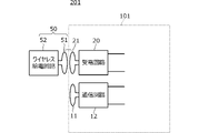
- FIG. 1 is a block diagram showing a configuration of an electronic card 101 and an electronic card system 201 according to the first embodiment.
- FIG. 2 is a block diagram showing another configuration of the electronic card 101 and the electronic card system 201 according to the first embodiment.
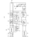
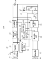
- FIG. 3 is a block diagram showing the configuration of the electronic card 101 according to the first embodiment.
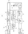
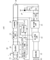
- FIG. 4 is a block diagram showing the configuration of the electronic card 102 according to the second embodiment.
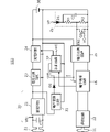
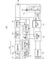
- FIG. 5 is a block diagram showing the configuration of the electronic card 103 according to the third embodiment.
- FIG. 6 is a block diagram showing the configuration of the electronic card 104 according to the fourth embodiment.
- FIG. 7 is a block diagram showing the configuration of the electronic card 105 according to the fifth embodiment.
- FIG. 8 is a block diagram showing the configuration of the electronic card 106 according to the sixth embodiment.
- 1 and 2 are block diagrams showing the configurations of the electronic card 101 and the electronic card system 201 according to the first embodiment.
- the electronic card system 201 includes an electronic card 101 and a reader / writer device 40. Further, the electronic card system 201 is composed of an electronic card 101 and a wireless power feeding device 50.
- the electronic card 101 is an example of the "wireless communication charging circuit system" according to the present invention, and the entire circuit is housed in an electronic card type housing.
- the electronic card 101 includes a power receiving coil 21, a power receiving circuit 20 connected to the power receiving coil 21, a communication antenna 11, and a communication circuit 12 connected to the communication antenna 11.
- the wireless power feeding device 50 includes a wireless power feeding coil 51 and a wireless power feeding circuit 52.
- the wireless power feeding device 50 is, for example, a smartphone when a wireless power feeding device of DC resonance technology, a smartphone having an NFC communication function, or the like is used as a charging device.
- the wireless power supply circuit 52 supplies alternating power to the wireless power supply coil 51 in the frequency band of the ISM band (industrial science and medical band) such as 2.4 GHz band, 5.7 GHz band, and 920 MHz band, or the frequency band of 6.78 MHz and 13.56 MHz. do.
- ISM band industrial science and medical band
- 2.4 GHz band 2.4 GHz band
- 5.7 GHz band 5.7 GHz band
- 920 MHz band or the frequency band of 6.78 MHz and 13.56 MHz. do.
- the power receiving coil 21 is magnetically coupled to the wireless power feeding coil 51, and the electronic card 101 wirelessly receives power from the wireless power feeding device 50.
- the reader / writer device 40 is composed of a reader / writer antenna 41 and a reader / writer circuit 42.
- the reader / writer antenna 41 is magnetically coupled to the communication antenna 11, and the electronic card 101 wirelessly communicates with the reader / writer device 40.
- NFC communication near field communication
- the communication circuit 12 is performed with the communication circuit 12 at a frequency in the 13.56 MHz band.
- the power receiving coil 21 is magnetically coupled to the reader / writer antenna 41, and the electronic card 101 wirelessly receives power from the reader / writer device 40.
- the electronic card 101 is, for example, a credit card-sized electronic device having a thickness of 0.76 mm.
- the electronic card 101 is, for example, a card-sized smartphone (a mobile phone equipped with a mobile operating system), a transportation IC card for displaying a balance, a one-time password card, a biometric authentication card, or the like.
- FIG. 3 is a block diagram showing the configuration of the electronic card 101.
- the electronic card 101 includes a power receiving coil 21, a power receiving circuit 20 connected to the power receiving coil 21, a communication antenna 11, a communication circuit 12 connected to the communication antenna 11, a power storage device 30, and a power receiving circuit 20.
- a charging circuit 24 connected to the power storage device 30, an electronic function circuit 16 connected to the communication circuit 12, a voltage conversion circuit 15 connected between the power storage device 30 and the electronic function circuit 16, and rectification.
- a voltage conversion circuit 31 connected to the output unit of the circuit 22 and a control circuit 32 for controlling the charging circuit 24 and the voltage conversion circuit 15 are provided.
- the control circuit 32 is composed of a microcomputer or a circuit including a microcomputer.
- the electronic card 101 actively operates using the power storage device 30 as a power source.
- the power receiving circuit 20 includes a power receiving resonance capacitor C1 connected to the power receiving coil 21 and a rectifier circuit 22.
- the power receiving coil 21 and the power receiving resonance capacitor C1 form a resonance circuit.
- the voltage conversion circuit 23 converts the output voltage (received voltage) of the power receiving circuit 20 into the voltage required for charging the power storage device 30.
- the control circuit 32 controls the operation of the charging circuit 24 and the operation of the voltage conversion circuit 15.
- the voltage conversion circuit 31 converts the output voltage of the rectifier circuit 22 into a voltage and outputs it as a power supply voltage for the control circuit 32.
- a switch SW is provided between the output unit of the voltage conversion circuit 31 and the power input unit of the control circuit 32.
- the output unit of the voltage conversion circuit 15 is connected to the power input unit of the electronic function circuit 16 and the control circuit 32.
- the switch SW is controlled by the output signal of the control circuit 32.
- the enable signal EN1 for the voltage conversion circuit 15 is connected to the power receiving detection circuit 25 by the diode D1, the capacitor C2, and the resistors R1 and R2.
- a switch element Q1 is provided in the output unit of the power receiving detection circuit 25.
- the switch element Q1 is composed of a MOS-FET.
- the switch element Q1 is controlled by the output signal of the control circuit 32.
- the voltage of the resonance circuit by the power receiving coil 21 and the power receiving resonance capacitor C1 is applied to the voltage input unit VP of the power receiving detection circuit 25.
- the diode D1 of the power receiving detection circuit 25 rectifies the voltage of the resonance circuit by the power receiving coil 21 and the power receiving resonance capacitor C1, and the capacitor C2 is smoothed. This rectified voltage is divided by the resistances R1 and R2.
- the enable signal EN1 for the voltage conversion circuit 15 becomes a high level.
- the switch element Q1 is on, this enable signal EN1 becomes low level.
- the operation of the electronic card 101 is as follows.
- the power receiving coil 21 receives power from the reader / writer antenna 41 of the reader / writer device 40.
- the voltage conversion circuit 23 converts the output voltage of the power receiving circuit 20 into a voltage and gives it to the charging circuit 24.
- the power receiving detection circuit 25 sets the enable signal EN1 for the voltage conversion circuit 15 to a high level.
- the voltage conversion circuit 15 converts the voltage of the power storage device 30 and supplies the power supply voltage to the electronic function circuit 16 and the control circuit 32.
- the electronic function circuit 16 operates using the output voltage of the voltage conversion circuit 15 as a power source.
- the communication antenna 11 is magnetically coupled to the reader / writer antenna 41, and the communication circuit 12 communicates with the reader / writer circuit 42.
- the electronic function circuit 16 inputs / outputs signals or data to / from the communication circuit 12.
- the communication circuit 12 causes the reader / writer device 40 to recognize (recognize the NFC-IC) and perform communication, and the control circuit 32 communicates with the reader / writer device 40.
- the power path is set so that the power used by the microcomputer of the control circuit 32 is supplied from the power storage device 30.
- the electronic function circuit 16 gives a communication completion signal to the control circuit 32 after the communication is completed.
- the control circuit 32 raises the control signal VC to a high level and turns on the switch element Q1.
- the enable signal EN1 for the voltage conversion circuit 15 becomes low level, so that the voltage conversion circuit 15 stops operating.
- the communication circuit 12 continues dummy communication with the reader / writer circuit 42 of the reader / writer device 40.
- the communication circuit 12 is an IC that performs NFC communication and does not require the power supply voltage supplied from the voltage conversion circuit 15.
- the reader / writer circuit 42 communicates for the recognition operation of the electronic card 101. Is.
- the power receiving circuit 20 wirelessly receives power from the reader / writer device 40.
- control circuit 32 activates the operation of the charging circuit 24.
- the charging circuit 24 starts charging the power storage device 30 with the output voltage of the voltage conversion circuit 23. This charging continues until the electronic card 101 is removed from the reader / writer device 40 and the dummy communication ends.
- the communication circuit 12 causes the reader / writer device 40 to recognize (recognize the NFC-IC) and operate the reader / writer device 40 to generate a magnetic field from the reader / writer device 40.
- the control circuit 32 sets the power path so that the power used by the microcomputer of the control circuit 32 is supplied from the power receiving circuit 20.
- the power receiving coil 21 receives power from the wireless power feeding coil 51 of the wireless power feeding device 50.
- the voltage conversion circuit 23 converts the output voltage of the power receiving circuit 20 into a voltage and gives it to the charging circuit 24.
- the power receiving detection circuit 25 sets the enable signal EN1 for the voltage conversion circuit 15 to a high level.
- the voltage conversion circuit 15 converts the voltage of the power storage device 30 and supplies the power supply voltage to the electronic function circuit 16 and the control circuit 32.
- the electronic function circuit 16 operates using the output voltage of the voltage conversion circuit 15 as a power source, and operates the control circuit 32.
- the control circuit 32 raises the control signal VC to a high level. As a result, the switch element Q1 is turned on and the enable signal EN1 for the voltage conversion circuit 15 becomes low level, so that the voltage conversion circuit 15 stops operating.
- control circuit 32 activates the operation of the charging circuit 24.
- the charging circuit 24 charges the power storage device 30 with the output voltage of the voltage conversion circuit 23.
- the electronic function circuit 16 gives a communication completion signal to the control circuit 32 after the communication is completed, but after a certain period of time from the start of the communication (after the elapse of the time required for the communication).
- a communication completion signal may be given to the control circuit 32.
- Second Embodiment a wireless communication charging circuit system in which the configuration for setting the power path is different from the example shown in the first embodiment will be illustrated.
- FIG. 4 is a block diagram showing the configuration of the electronic card 102 according to the second embodiment.
- the configuration of the voltage conversion circuit 31 and the control circuit 32 is different from that of the electronic card 101 shown in FIG.
- the voltage conversion circuit 31 includes an input terminal for the enable signal EN2.
- the control circuit 32 outputs an enable signal EN2 for the voltage conversion circuit 31.
- a power supply voltage is supplied to the control circuit 32 from the voltage conversion circuit 31 or the voltage conversion circuit 15.
- the operation of the electronic card 102 is as follows.
- the power receiving coil 21 receives power from the reader / writer antenna 41 of the reader / writer device 40.
- the voltage conversion circuit 23 converts the output voltage of the power receiving circuit 20 into a voltage and gives it to the charging circuit 24.
- the power receiving detection circuit 25 sets the enable signal EN1 for the voltage conversion circuit 15 to a high level.
- the voltage conversion circuit 15 converts the voltage of the power storage device 30 and supplies the power supply voltage to the electronic function circuit 16 and the control circuit 32.
- the electronic function circuit 16 operates using the output voltage of the voltage conversion circuit 15 as a power source.
- the communication antenna 11 is magnetically coupled to the reader / writer antenna 41, and the communication circuit 12 communicates with the reader / writer circuit 42.
- the electronic function circuit 16 inputs / outputs signals or data to / from the communication circuit 12.
- the electronic function circuit 16 gives a communication completion signal to the control circuit 32 after the communication is completed.
- the control circuit 32 raises the control signal VC to a high level and turns on the switch element Q1.
- the enable signal EN1 for the voltage conversion circuit 15 becomes low level, so that the voltage conversion circuit 15 stops operating.
- the communication circuit 12 continues dummy communication with the reader / writer circuit 42 of the reader / writer device 40.
- This dummy communication is communication for the reader / writer circuit 42 to recognize the electronic card 101.
- the power receiving circuit 20 wirelessly receives power from the reader / writer device 40. Therefore, the control circuit 32 operates using the output voltage of the voltage conversion circuit 31 as a power source.
- control circuit 32 activates the operation of the charging circuit 24. Then, the charging circuit 24 charges the power storage device 30 with the output voltage of the voltage conversion circuit 23.
- the power receiving coil 21 receives power from the wireless power feeding coil 51 of the wireless power feeding device 50.
- the voltage conversion circuit 23 converts the output voltage of the power receiving circuit 20 into a voltage and gives it to the charging circuit 24.
- the power receiving detection circuit 25 sets the enable signal EN1 for the voltage conversion circuit 15 to a high level.
- the voltage conversion circuit 15 converts the voltage of the power storage device 30 and supplies the power supply voltage to the electronic function circuit 16 and the control circuit 32.
- the electronic function circuit 16 operates using the output voltage of the voltage conversion circuit 15 as a power source, and operates the control circuit 32.
- the control circuit 32 sets the enable signal EN2 for the voltage conversion circuit 31 to a high level (valid). As a result, the output voltage of the voltage conversion circuit 31 is supplied as the power supply voltage to the control circuit 32.
- the control circuit 32 raises the control signal VC to a high level. As a result, the switch element Q1 is turned on and the enable signal EN1 for the voltage conversion circuit 15 becomes low level, so that the voltage conversion circuit 15 stops operating.
- control circuit 32 activates the operation of the charging circuit 24.
- the charging circuit 24 charges the power storage device 30 with the output voltage of the voltage conversion circuit 23.
- FIG. 5 is a block diagram showing the configuration of the electronic card 103 according to the third embodiment.
- the configuration of the switch SW is different from that of the electronic card 101 shown in FIG.
- the switch portion is composed of the diode D2.
- Other configurations are as shown in the first embodiment.
- the outline operation of the electronic card 103 is as follows.
- the power receiving coil 21 receives power from the wireless power feeding coil 51 of the wireless power feeding device 50.
- the voltage conversion circuit 23 converts the output voltage of the power receiving circuit 20 into a voltage and gives it to the charging circuit 24.
- the power receiving detection circuit 25 sets the enable signal EN1 for the voltage conversion circuit 15 to a high level.
- the voltage conversion circuit 15 converts the voltage of the power storage device 30 and supplies the power supply voltage to the electronic function circuit 16 and the control circuit 32.
- the output voltage of the voltage conversion circuit 31 is lower than the output voltage of the voltage conversion circuit 15.
- the output voltage of the voltage conversion circuit 31 is 3.0V
- the output voltage of the voltage conversion circuit 15 is 3.3V. Therefore, the electronic function circuit 16 operates using the output voltage of the voltage conversion circuit 15 as a power source. Further, the control circuit 32 operates at the output voltage of the voltage conversion circuit 15.
- the control circuit 32 raises the control signal VC to a high level. As a result, the switch element Q1 is turned on and the enable signal EN1 for the voltage conversion circuit 15 becomes low level, so that the voltage conversion circuit 15 stops operating.
- control circuit 32 activates the operation of the charging circuit 24.
- the charging circuit 24 charges the power storage device 30 with the output voltage of the voltage conversion circuit 23.
- FIG. 6 is a block diagram showing the configuration of the electronic card 104 according to the fourth embodiment. Unlike the electronic card 103 shown in FIG. 5, this electronic card 104 is a switch circuit using switch elements Q2 and Q3 and a resistor R3 between the output unit of the voltage conversion circuit 15 and the power supply voltage input unit of the control circuit 32. Is configured. Further, the output of the power receiving detection circuit 25 is connected to the gate of the switch element Q2.
- the outline operation of the electronic card 104 is as follows.
- the power receiving coil 21 receives power from the reader / writer antenna 41 of the reader / writer device 40.
- the voltage conversion circuit 23 converts the output voltage of the power receiving circuit 20 into a voltage and gives it to the charging circuit 24.
- the output voltage of the voltage conversion circuit 31 is lower than the output voltage of the voltage conversion circuit 15.
- the output voltage of the voltage conversion circuit 31 is 3.0V
- the output voltage of the voltage conversion circuit 15 is 3.3V. Therefore, the electronic function circuit 16 operates using the output voltage of the voltage conversion circuit 15 as a power source, and inputs / outputs a signal to / from the communication circuit 12. Further, the control circuit 32 operates at the output voltage of the voltage conversion circuit 15.
- the communication antenna 11 is magnetically coupled to the reader / writer antenna 41, and the communication circuit 12 communicates with the reader / writer circuit 42.
- the electronic function circuit 16 gives a communication completion signal to the control circuit 32 after the communication is completed. As a result, the control circuit 32 stops the operation of the voltage conversion circuit 15. Further, the control circuit 32 sets the control signal VC to a high level and turns on the switch element Q1. As a result, the switch elements Q2 and Q3 are turned off, and the power supply from the voltage conversion circuit 15 to the control circuit 32 is stopped.
- the communication circuit 12 continues dummy communication with the reader / writer circuit 42 of the reader / writer device 40.
- This dummy communication is communication for the reader / writer circuit 42 to recognize the electronic card 101.
- the power receiving circuit 20 wirelessly receives power from the reader / writer device 40. Therefore, the control circuit 32 operates using the output voltage of the voltage conversion circuit 31 as a power source.
- control circuit 32 activates the operation of the charging circuit 24.
- the charging circuit 24 charges the power storage device 30 with the output voltage of the voltage conversion circuit 23.
- the power receiving coil 21 receives power from the wireless power feeding coil 51 of the wireless power feeding device 50.
- the voltage conversion circuit 23 converts the output voltage of the power receiving circuit 20 into a voltage and gives it to the charging circuit 24.
- the electronic function circuit 16 operates using the output voltage of the voltage conversion circuit 15 as a power source, and operates the control circuit 32.
- the output voltage of the voltage conversion circuit 31 is lower than the output voltage of the voltage conversion circuit 15.
- the output voltage of the voltage conversion circuit 31 is 3.0V
- the output voltage of the voltage conversion circuit 15 is 3.3V. Therefore, the electronic function circuit 16 operates using the output voltage of the voltage conversion circuit 15 as a power source, and inputs / outputs a signal to / from the communication circuit 12. Further, the control circuit 32 operates at the output voltage of the voltage conversion circuit 15.
- the control circuit 32 raises the control signal VC to a high level. As a result, the switch element Q1 is turned on and the switch elements Q2 and Q3 are turned off, so that the power supply from the voltage conversion circuit 15 to the control circuit 32 is stopped.
- control circuit 32 activates the operation of the charging circuit 24.
- the charging circuit 24 charges the power storage device 30 with the output voltage of the voltage conversion circuit 23.
- FIG. 7 is a block diagram showing the configuration of the electronic card 105 according to the fifth embodiment.
- the supply power switching circuit 33 for controlling the switch SW is provided.
- the switch SW is controlled not only by the control circuit 32 but also by the supply power switching circuit 33.
- Other configurations are as shown in the first embodiment.
- the supply power switching circuit 33 controls the switch SW according to the output voltage of the charging circuit 24 and the voltage of the power storage device 30. Further, the supply power switching circuit 33 detects the remaining amount of the power storage device 30. During the communication period by the communication circuit 12, if the remaining amount of the power storage device 30 is a predetermined amount or more, the supply power switching circuit 33 shuts off the switch SW1. As a result, the power supply voltage for the control circuit 32 is supplied from the voltage conversion circuit 15 (from the power storage device 30). When the remaining amount of the power storage device 30 is less than a predetermined amount, the supply power switching circuit 33 conducts the switch SW. As a result, the power supply voltage for the control circuit 32 is supplied from the power receiving circuit 20 (from the voltage conversion circuit 31).
- the supply power switching circuit 33 corresponds to the power storage device remaining amount detecting means for detecting the remaining amount of the power storage device 30.
- the function of the control circuit 32 can be maintained, and if the remaining amount of the power storage device 30 is sufficient, the alternating magnetic field used for communication is used. Even if the energy of the above is coupled to the power receiving coil 21, the power is not consumed by the control circuit 32, so that the shortening of the communication distance and the deterioration of the communication quality are suppressed.
- ⁇ 6th Embodiment a wireless communication charging circuit system in which the configuration of the power supply switching means for the control circuit 32 is different from that of the embodiments shown so far will be exemplified.
- FIG. 8 is a block diagram showing the configuration of the electronic card 106 according to the sixth embodiment.
- the supply power switching circuit 33 and the diode D2 are provided.
- Other configurations are as shown in the third embodiment.
- the supply power switching circuit 33 detects the received voltage of the power receiving circuit 20.
- the supply power switching circuit 33 supplies power to the control circuit 32 from the power receiving circuit 20 when the power received voltage by the power receiving circuit 20 exceeds a predetermined value, and controls when the power received voltage by the power receiving circuit 20 does not reach the predetermined value.
- the electric power to the circuit 32 is supplied from the power storage device 30.
- the enable signal EN1 of the voltage conversion circuit 15 is enabled by the output signal of the power reception detection circuit 25, and the voltage conversion circuit 15 operates. Since the output voltage of the voltage conversion circuit 15 is higher than the output voltage of the voltage conversion circuit 31, the control circuit 32 operates with the power of the power storage device 30. At this time, if the supply power switching circuit 33 detects that the received voltage by the power receiving circuit 20 is equal to or higher than the threshold value, a control signal is given to the control circuit 32. As a result, the control circuit 32 sets the control signal VC to a high level. As a result, the voltage conversion circuit 15 stops operating, and the control circuit 32 operates with the power received from the power receiving circuit 20.
- the control circuit 32 activates the operation of the charging circuit 24. Then, the charging circuit 24 charges the power storage device 30 with the output voltage of the voltage conversion circuit 23.
- the received energy is used as the power to the control circuit 32, so that the power consumption of the battery can be reduced and the energy of the alternating magnetic field can be effectively utilized. ..
- the energy of the storage device 30 is used as the electric power to the control circuit 32, so that the shortening of the communication distance and the deterioration of the communication quality are suppressed.
Landscapes
- Engineering & Computer Science (AREA)
- Computer Networks & Wireless Communication (AREA)
- Power Engineering (AREA)
- Signal Processing (AREA)
- Near-Field Transmission Systems (AREA)
- Charge And Discharge Circuits For Batteries Or The Like (AREA)
Abstract
ワイヤレス通信充電回路システムを構成する電子カード(101)は、受電コイル(21)と、受電回路(20)と、蓄電デバイス(30)と、充電回路(24)と、蓄電デバイス(30)に接続されて所定の電源電圧を発生する電圧変換回路(15)と、通信アンテナ(11)と、電圧変換回路(15)の出力電力で通信を行う通信回路(12)と、電圧変換回路(15)及び充電回路(24)の制御を行う制御回路(32)を備える。制御回路(32)は、通信期間では通信回路(12)が通信を行い、マイコンが使用する電力を蓄電デバイス(30)から供給するように電力経路を設定し、充電期間では通信回路(12)が認識させたリーダライタ装置が磁界を発生させ、マイコンが使用する電力を受電回路(20)から供給するように電力経路を設定する。
Description
本発明は、ワイヤレスで電力を受電するとともに内部の回路への電力供給及び内部の蓄電デバイスへの充電制御を行う機能及びワイヤレスで通信を行う機能を備えるワイヤレス通信充電回路システムに関する。
二次電池を備えるICカードの例として、特許文献1に指紋認証付ICカードが示されている。このICカードは、指紋読取りセンサを備え、リーダーから供給される電力を蓄電回路で蓄電し、蓄電回路の出力電圧が既定値に達すると装置制御回路と指紋処理回路に放電し、指紋認証が成功した場合に、リーダーとの間の送受信を許可し、その後は、リーダーとの間の送受信を禁止し、装置制御回路及び指紋処理回路への放電をオフするように構成されている。
近距離無線通信機能を備えたワイヤレス充電電子カードでは、カード内の制御回路は二次電池の充放電や通信回路への電力供給の管理を行う。その制御回路は受電電力によって動作し、二次電池を充電する場合に充電回路を動作させる。また、その制御回路は、近距離無線通信を行う場合に、充電回路の動作を停止させ、通信回路を動作させる。この様に、制御回路を用いて、充電回路の動作と通信回路の動作は切り替えられる。
近距離無線通信を行う場合において、制御回路が受電電力によって動作すると、制御回路は近距離無線通信に用いる交番磁界のエネルギーを消費するので、近距離無線通信における通信距離や通信品質の低下を招いてしまう。二次電池から制御回路に電力を供給する構成とすれば通信特性は改善されるが、通信特性が十分に担保されている場合においても、制御回路は常に二次電池の電力を消費することとなり、充電時間や待機電力が増加してしまい、受電電力が十分に活用されない。
そこで、本発明の目的は、通信距離の短縮化や通信品質の低下を抑制し、かつ受電電力を有効に活用できるようにしたワイヤレス通信充電回路システムを提供することにある。
本開示の一例としてのワイヤレス通信充電回路システムは、リーダライタ装置の送信アンテナ又はワイヤレス送電コイルに磁界結合する受電コイルと、前記受電コイルに電気的に接続され、前記受電コイルに誘導される電力を受ける受電回路と、蓄電デバイスと、前記蓄電デバイスに接続され、前記受電回路から供給される電力により前記蓄電デバイスを充電する充電回路と、前記蓄電デバイスに接続されて所定の電圧に変換する電圧変換回路と、前記電圧変換回路に電気的に接続され、電力を消費する負荷と、通信アンテナと、前記通信アンテナに電気的に接続され、前記通信アンテナを用いて通信を行う通信回路と、前記電圧変換回路の動作と停止及び前記充電回路の動作と停止の制御を行うマイコンを備えた制御回路と、を備える。そして、前記リーダライタ装置と前記通信アンテナを用いて通信を行う期間では、前記通信回路は、前記リーダライタ装置に認識させて通信を行い、前記制御回路は、前記蓄電デバイスから前記マイコンが使用する電力を供給するように電力経路を設定し、前記リーダライタ装置により前記蓄電デバイスの充電を行う期間では、前記通信回路は、前記リーダライタ装置に認識させて動作させることで磁界を発生させ、前記制御回路は、前記マイコンが使用する電力を前記受電回路から供給するように電力経路を設定する。
上記構成により、通信期間では蓄電デバイスから制御回路に電力が供給され、充電期間では受電回路から制御回路に電力が供給される。
本発明によれば、通信期間における通信距離の短縮化や通信品質の低下が抑制され、かつ充電期間における受電電力が有効に活用されるワイヤレス通信充電回路システムが得られる。
《第1の実施形態》
図1、図2は、第1の実施形態に係る電子カード101及び電子カードシステム201の構成を示すブロック図である。この電子カードシステム201は、電子カード101とリーダライタ装置40とで構成される。また、電子カードシステム201は、電子カード101とワイヤレス給電装置50とで構成される。電子カード101は本発明に係る「ワイヤレス通信充電回路システム」の一例であり、全体の回路が電子カード型の筐体に収められている。
図1、図2は、第1の実施形態に係る電子カード101及び電子カードシステム201の構成を示すブロック図である。この電子カードシステム201は、電子カード101とリーダライタ装置40とで構成される。また、電子カードシステム201は、電子カード101とワイヤレス給電装置50とで構成される。電子カード101は本発明に係る「ワイヤレス通信充電回路システム」の一例であり、全体の回路が電子カード型の筐体に収められている。
図1において、電子カード101内の構成は一部のみを表れている。電子カード101は、受電コイル21と、この受電コイル21に接続された受電回路20と、通信アンテナ11と、この通信アンテナ11に接続された通信回路12と、を備える。ワイヤレス給電装置50はワイヤレス給電コイル51とワイヤレス給電回路52とで構成されている。
ワイヤレス給電装置50は、例えば直流共鳴技術のワイヤレス給電装置や、NFC通信機能を有するスマートフォン等を充電装置として利用する場合のスマートフォンである。
ワイヤレス給電回路52は、2.4GHz帯、5.7GHz帯、920MHz帯などのISMバンド(産業科学医療用バンド)の周波数帯、または6.78MHz、13.56MHzの周波数帯でワイヤレス給電コイル51に交番電力を供給する。
図1に示す例では、受電コイル21はワイヤレス給電コイル51と磁界結合して、電子カード101は、ワイヤレス給電装置50からワイヤレスで電力を受電する。
図2において、リーダライタ装置40はリーダライタアンテナ41とリーダライタ回路42とで構成されている。
図2に示す例では、リーダライタアンテナ41は通信アンテナ11と磁界結合して、電子カード101は、リーダライタ装置40とワイヤレスで通信する。例えば13.56MHz帯の周波数で通信回路12とNFC通信(近距離無線通信)を行う。
また、受電コイル21はリーダライタアンテナ41と磁界結合して、電子カード101は、リーダライタ装置40からワイヤレスで電力を受電する。
電子カード101は例えば厚み0.76mmのクレジットカードサイズの電子機器である。この電子カード101は、例えばカードサイズのスマートフォン(モバイル向けオペレーティングシステムを備えた携帯電話)、残高表示を行う交通系ICカード、ワンタイムパスワードカード、生体認証カード等である。
図3は電子カード101の構成を示すブロック図である。電子カード101は、受電コイル21と、この受電コイル21に接続された受電回路20と、通信アンテナ11と、この通信アンテナ11に接続された通信回路12と、蓄電デバイス30と、受電回路20と蓄電デバイス30との間に接続された充電回路24と、通信回路12に接続された電子機能回路16と、蓄電デバイス30と電子機能回路16との間に接続された電圧変換回路15と、整流回路22の出力部に接続された電圧変換回路31と、充電回路24及び電圧変換回路15を制御する制御回路32と、を備える。制御回路32はマイコン又はマイコンを備える回路で構成される。電子カード101は、蓄電デバイス30を電源としてアクティブ動作する。
受電回路20は、受電コイル21に接続された受電共振キャパシタC1と整流回路22とを含む。受電コイル21と受電共振キャパシタC1とは共振回路を構成する。
電圧変換回路23は、受電回路20の出力電圧(受電電圧)を、蓄電デバイス30の充電に要する電圧に変換する。
制御回路32は充電回路24の動作及び電圧変換回路15の動作を制御する。電圧変換回路31は整流回路22の出力電圧を電圧変換して制御回路32に対する電源電圧として出力する。
電圧変換回路31の出力部と制御回路32の電源入力部との間にはスイッチSWが設けられている。電圧変換回路15の出力部は電子機能回路16及び制御回路32の電源入力部に接続されている。スイッチSWは制御回路32の出力信号によって制御される。
電圧変換回路15に対するイネーブル信号EN1には、ダイオードD1、キャパシタC2及び抵抗R1,R2による受電検出回路25が接続されている。この受電検出回路25の出力部にはスイッチ素子Q1が設けられている。スイッチ素子Q1はMOS-FETで構成されている。このスイッチ素子Q1は制御回路32の出力信号によって制御される。受電検出回路25の電圧入力部VPには、受電コイル21と受電共振キャパシタC1による共振回路の電圧が印加される。
上記受電検出回路25のダイオードD1は受電コイル21と受電共振キャパシタC1による共振回路の電圧を整流し、キャパシタC2は平滑する。この整流電圧は抵抗R1,R2で分圧される。電圧入力部VPの電圧が所定値以上であるとき、電圧変換回路15に対するイネーブル信号EN1はハイレベルとなる。スイッチ素子Q1がオンのとき、このイネーブル信号EN1はローレベルとなる。
電子カード101の動作は次のとおりである。
[電子カード101をリーダライタ装置40へ近接させた場合]
(a)受電コイル21はリーダライタ装置40のリーダライタアンテナ41から電力を受ける。電圧変換回路23は受電回路20の出力電圧を電圧変換して充電回路24へ与える。
(a)受電コイル21はリーダライタ装置40のリーダライタアンテナ41から電力を受ける。電圧変換回路23は受電回路20の出力電圧を電圧変換して充電回路24へ与える。
(b)受電コイル21がリーダライタ装置40のリーダライタアンテナ41から電力を受けることによって、受電検出回路25は電圧変換回路15に対するイネーブル信号EN1をハイレベルとする。これにより、電圧変換回路15は蓄電デバイス30の電圧を変換して電子機能回路16及び制御回路32へ電源電圧を供給する。
(c)電子機能回路16は電圧変換回路15の出力電圧を電源として動作する。
(d)通信アンテナ11はリーダライタアンテナ41と磁界結合し、通信回路12はリーダライタ回路42と通信する。電子機能回路16は通信回路12との間で信号又はデータを入出力する。
このように、通信アンテナ11を用いてリーダライタ装置40と通信を行う期間では、通信回路12は、リーダライタ装置40に認識(NFC-ICを認識)させて通信を行い、制御回路32は、制御回路32のマイコンが使用する電力を蓄電デバイス30から供給するように電力経路を設定する。
(e)電子機能回路16は、通信の完了後、制御回路32へ通信完了信号を与える。これにより、制御回路32は制御信号VCをハイレベルにしてスイッチ素子Q1をオンさせる。これにより、電圧変換回路15に対するイネーブル信号EN1がローレベルになるので、電圧変換回路15は動作を停止する。
ただし、通信回路12は、リーダライタ装置40のリーダライタ回路42とのダミーの通信を継続する。(通信回路12はNFC通信を行うICであり、電圧変換回路15から供給される電源電圧は必要としない。)このダミーの通信は、リーダライタ回路42が電子カード101の認識動作のための通信である。このダミーの通信を行うことにより、受電回路20はリーダライタ装置40からワイヤレスで電力を受電する。
(f)その後、制御回路32は充電回路24の動作を有効化する。これにより、充電回路24は電圧変換回路23の出力電圧で蓄電デバイス30の充電を開始する。この充電は、電子カード101がリーダライタ装置40から取り除かれて上記ダミーの通信が終了するまで継続される。
したがって、充電期間では、電圧変換回路15、電子機能回路16及び制御回路32による電力消費が殆ど無くなる。
このように、リーダライタ装置40により蓄電デバイス30の充電を行う期間では、通信回路12は、リーダライタ装置40に認識(NFC-ICを認識)させて動作させることでリーダライタ装置40から磁界を発生させ、制御回路32は、制御回路32のマイコンが使用する電力を受電回路20から供給するように電力経路を設定する。
[電子カード101をワイヤレス給電装置50へ載置した場合]
(a)受電コイル21はワイヤレス給電装置50のワイヤレス給電コイル51から電力を受ける。電圧変換回路23は受電回路20の出力電圧を電圧変換して充電回路24へ与える。
(a)受電コイル21はワイヤレス給電装置50のワイヤレス給電コイル51から電力を受ける。電圧変換回路23は受電回路20の出力電圧を電圧変換して充電回路24へ与える。
(b)受電コイル21がワイヤレス給電装置50のワイヤレス給電コイル51から電力を受けることによって、受電検出回路25は電圧変換回路15に対するイネーブル信号EN1をハイレベルとする。これにより、電圧変換回路15は蓄電デバイス30の電圧を変換して電子機能回路16及び制御回路32へ電源電圧を供給する。
(c)電子機能回路16は電圧変換回路15の出力電圧を電源として動作し、制御回路32を動作させる。
(d)制御回路32はスイッチSWを導通させる。これにより、電圧変換回路31の出力電圧が制御回路32に対する電源電圧として供給される。
(e)制御回路32は制御信号VCをハイレベルにする。これにより、スイッチ素子Q1がオンして、電圧変換回路15に対するイネーブル信号EN1がローレベルになるので、電圧変換回路15は動作を停止する。
(f)その後、制御回路32は充電回路24の動作を有効化する。これにより、充電回路24は電圧変換回路23の出力電圧で蓄電デバイス30を充電する。
したがって、充電期間では、電圧変換回路15、電子機能回路16及び制御回路32による電力消費が殆ど無くなる。
上記構成により、通信期間では蓄電デバイス30から制御回路32に電力が供給され、充電期間では受電回路20から制御回路32に電力が供給される。電子機能回路16の情報を通信する通信期間では、通信に用いる交番磁界のエネルギーが受電コイル21に結合しても、その電力は制御回路32で消費されない。その結果、通信距離の短縮化や通信品質の低下が抑制される。一方、充電期間においては、電圧変換回路15、電子機能回路16及び制御回路32による電力消費が殆ど無くなる。そのため、待機電力が低減されて受電電力が有効に利用され、蓄電デバイス30の充電時間が短縮化される。
なお、以上に示した例では、電子機能回路16は、通信の完了後に制御回路32へ通信完了信号を与えるようにしたが、通信の開始から一定時間後(通信に要する時間の経過後)に制御回路32へ通信完了信号を与えるようにしてもよい。
上記構成により、通信期間では蓄電デバイス30から制御回路32に電力が供給され、充電期間では受電回路20から制御回路32に電力が供給される。通信期間では、通信に用いる交番磁界のエネルギーが受電コイル21に結合しても、その電力は制御回路32で消費されない。その結果、通信期間において、通信距離の短縮化や通信品質の低下が抑制される。一方、充電期間においては、電圧変換回路15、電子機能回路16及び制御回路32が蓄電デバイス30の電力を消費しない。そのため、待機電力が低減されて受電電力が有効に利用され、蓄電デバイス30の充電時間が短縮化される。
《第2の実施形態》
第2の実施形態では、電力経路を設定する構成が第1の実施形態で示した例とは異なるワイヤレス通信充電回路システムについて例示する。
第2の実施形態では、電力経路を設定する構成が第1の実施形態で示した例とは異なるワイヤレス通信充電回路システムについて例示する。
図4は第2の実施形態に係る電子カード102の構成を示すブロック図である。図3に示した電子カード101とは、電圧変換回路31及び制御回路32の構成が異なる。電圧変換回路31はイネーブル信号EN2の入力端子を備える。制御回路32は電圧変換回路31に対するイネーブル信号EN2を出力する。制御回路32には電圧変換回路31又は電圧変換回路15から電源電圧が供給される。
電子カード102の動作は次のとおりである。
[電子カード102をリーダライタ装置40へ近接させた場合]
(a)受電コイル21はリーダライタ装置40のリーダライタアンテナ41から電力を受ける。電圧変換回路23は受電回路20の出力電圧を電圧変換して充電回路24へ与える。
(a)受電コイル21はリーダライタ装置40のリーダライタアンテナ41から電力を受ける。電圧変換回路23は受電回路20の出力電圧を電圧変換して充電回路24へ与える。
(b)受電コイル21がリーダライタ装置40のリーダライタアンテナ41から電力を受けることによって、受電検出回路25は電圧変換回路15に対するイネーブル信号EN1をハイレベルとする。これにより、電圧変換回路15は蓄電デバイス30の電圧を変換して電子機能回路16及び制御回路32へ電源電圧を供給する。
(c)電子機能回路16は電圧変換回路15の出力電圧を電源として動作する。
(d)通信アンテナ11はリーダライタアンテナ41と磁界結合し、通信回路12はリーダライタ回路42と通信する。電子機能回路16は通信回路12との間で信号又はデータを入出力する。
(e)電子機能回路16は、通信の完了後、制御回路32へ通信完了信号を与える。これにより、制御回路32は制御信号VCをハイレベルにしてスイッチ素子Q1をオンさせる。これにより、電圧変換回路15に対するイネーブル信号EN1がローレベルになるので、電圧変換回路15は動作を停止する。
ただし、通信回路12は、リーダライタ装置40のリーダライタ回路42とのダミーの通信を継続する。このダミーの通信は、リーダライタ回路42が電子カード101の認識動作のための通信である。このダミーの通信を行うことにより、受電回路20はリーダライタ装置40からワイヤレスで電力を受電する。したがって、制御回路32は電圧変換回路31の出力電圧を電源にして動作する。
(f)その後、制御回路32は充電回路24の動作を有効化する。そして、充電回路24は電圧変換回路23の出力電圧で蓄電デバイス30を充電する。
したがって、充電期間では、電圧変換回路15、電子機能回路16及び制御回路32による電力消費が殆ど無くなる。
[電子カード102をワイヤレス給電装置50へ載置した場合]
(a)受電コイル21はワイヤレス給電装置50のワイヤレス給電コイル51から電力を受ける。電圧変換回路23は受電回路20の出力電圧を電圧変換して充電回路24へ与える。
(a)受電コイル21はワイヤレス給電装置50のワイヤレス給電コイル51から電力を受ける。電圧変換回路23は受電回路20の出力電圧を電圧変換して充電回路24へ与える。
(b)受電コイル21がワイヤレス給電装置50のワイヤレス給電コイル51から電力を受けることによって、受電検出回路25は電圧変換回路15に対するイネーブル信号EN1をハイレベルとする。これにより、電圧変換回路15は蓄電デバイス30の電圧を変換して電子機能回路16及び制御回路32へ電源電圧を供給する。
(c)電子機能回路16は電圧変換回路15の出力電圧を電源として動作し、制御回路32を動作させる。
(d)制御回路32は電圧変換回路31に対するイネーブル信号EN2をハイレベル(有効)にする。これにより、電圧変換回路31の出力電圧が制御回路32に対する電源電圧として供給される。
(e)制御回路32は制御信号VCをハイレベルにする。これにより、スイッチ素子Q1がオンして、電圧変換回路15に対するイネーブル信号EN1がローレベルになるので、電圧変換回路15は動作を停止する。
(f)その後、制御回路32は充電回路24の動作を有効化する。これにより、充電回路24は電圧変換回路23の出力電圧で蓄電デバイス30を充電する。
したがって、充電期間では、電圧変換回路15、電子機能回路16及び制御回路32による電力消費が殆ど無くなる。
以上の構成により、第1の実施形態で示した例と同様の作用効果を奏する。
《第3の実施形態》
第3の実施形態では、電力経路を設定する構成が第1の実施形態で示した例とは異なるワイヤレス通信充電回路システムについて例示する。
第3の実施形態では、電力経路を設定する構成が第1の実施形態で示した例とは異なるワイヤレス通信充電回路システムについて例示する。
図5は第3の実施形態に係る電子カード103の構成を示すブロック図である。
図1に示した電子カード101とはスイッチSWの構成が異なる。図5に示す例では、スイッチ部分をダイオードD2で構成している。その他の構成は第1の実施形態で示したとおりである。
電子カード103の概略動作は次のとおりである。
[電子カード103をリーダライタ装置40へ近接させた場合]
第1の実施形態で示した電子カード101又は第2の実施形態で示した電子カード102の動作を同様である。
第1の実施形態で示した電子カード101又は第2の実施形態で示した電子カード102の動作を同様である。
[電子カード103をワイヤレス給電装置50へ載置した場合]
(a)受電コイル21はワイヤレス給電装置50のワイヤレス給電コイル51から電力を受ける。電圧変換回路23は受電回路20の出力電圧を電圧変換して充電回路24へ与える。
(a)受電コイル21はワイヤレス給電装置50のワイヤレス給電コイル51から電力を受ける。電圧変換回路23は受電回路20の出力電圧を電圧変換して充電回路24へ与える。
(b)受電コイル21がワイヤレス給電装置50のワイヤレス給電コイル51から電力を受けることによって、受電検出回路25は電圧変換回路15に対するイネーブル信号EN1をハイレベルとする。これにより、電圧変換回路15は蓄電デバイス30の電圧を変換して電子機能回路16及び制御回路32へ電源電圧を供給する。
(c)電圧変換回路31の出力電圧は電圧変換回路15の出力電圧より低い。例えば、電圧変換回路31の出力電圧は3.0V、電圧変換回路15の出力電圧は3.3Vである。そのため、電子機能回路16は電圧変換回路15の出力電圧を電源として動作する。また、制御回路32は電圧変換回路15の出力電圧で動作する。
(d)制御回路32は制御信号VCをハイレベルにする。これにより、スイッチ素子Q1がオンして、電圧変換回路15に対するイネーブル信号EN1がローレベルになるので、電圧変換回路15は動作を停止する。
(e)その後、制御回路32は充電回路24の動作を有効化する。これにより、充電回路24は電圧変換回路23の出力電圧で蓄電デバイス30を充電する。
したがって、充電期間では、電圧変換回路15、電子機能回路16及び制御回路32による電力消費が殆ど無くなり、制御回路32は電圧変換回路31の出力電圧によって動作する。
以上の構成により、第1、第2の実施形態で示した例と同様の作用効果を奏する。
《第4の実施形態》
第4の実施形態では、電力経路を設定する構成がこれまでの実施形態で示した例とは異なるワイヤレス通信充電回路システムについて例示する。
第4の実施形態では、電力経路を設定する構成がこれまでの実施形態で示した例とは異なるワイヤレス通信充電回路システムについて例示する。
図6は第4の実施形態に係る電子カード104の構成を示すブロック図である。この電子カード104は、図5に示した電子カード103とは異なり、電圧変換回路15の出力部と制御回路32の電源電圧入力部との間に、スイッチ素子Q2,Q3及び抵抗R3によるスイッチ回路が構成されている。また、受電検出回路25の出力はスイッチ素子Q2のゲートに接続されている。
電子カード104の概略動作は次のとおりである。
[電子カード104をリーダライタ装置40へ近接させた場合]
(a)受電コイル21はリーダライタ装置40のリーダライタアンテナ41から電力を受ける。電圧変換回路23は受電回路20の出力電圧を電圧変換して充電回路24へ与える。
(a)受電コイル21はリーダライタ装置40のリーダライタアンテナ41から電力を受ける。電圧変換回路23は受電回路20の出力電圧を電圧変換して充電回路24へ与える。
(b)受電コイル21がリーダライタ装置40のリーダライタアンテナ41から電力を受けることによって、受電検出回路25はスイッチ素子Q2にゲートに対する電圧をハイレベルとする。これにより、スイッチ素子Q3は導通し、電圧変換回路15の出力電圧は電子機能回路16及び制御回路32へ電源電圧として供給される。
(c)電圧変換回路31の出力電圧は電圧変換回路15の出力電圧より低い。例えば、電圧変換回路31の出力電圧は3.0V、電圧変換回路15の出力電圧は3.3Vである。そのため、電子機能回路16は電圧変換回路15の出力電圧を電源として動作し、通信回路12との間で信号を入出力する。また、制御回路32は電圧変換回路15の出力電圧で動作する。
(d)通信アンテナ11はリーダライタアンテナ41と磁界結合し、通信回路12はリーダライタ回路42と通信する。
(e)電子機能回路16は、通信の完了後、制御回路32へ通信完了信号を与える。これにより、制御回路32は電圧変換回路15の動作を停止させる。また、制御回路32は制御信号VCをハイレベルにしてスイッチ素子Q1をオンさせる。これにより、スイッチ素子Q2,Q3はオフして、電圧変換回路15から制御回路32への電力供給は停止する。
ただし、通信回路12は、リーダライタ装置40のリーダライタ回路42とのダミーの通信を継続する。このダミーの通信は、リーダライタ回路42が電子カード101の認識動作のための通信である。このダミーの通信を行うことにより、受電回路20はリーダライタ装置40からワイヤレスで電力を受電する。したがって、制御回路32は電圧変換回路31の出力電圧を電源にして動作する。
(f)その後、制御回路32は充電回路24の動作を有効化する。これにより、充電回路24は電圧変換回路23の出力電圧で蓄電デバイス30を充電する。
したがって、充電期間では制御回路32及び電圧変換回路15による電力消費が殆ど無くなる。
[電子カード104をワイヤレス給電装置50へ載置した場合]
(a)受電コイル21はワイヤレス給電装置50のワイヤレス給電コイル51から電力を受ける。電圧変換回路23は受電回路20の出力電圧を電圧変換して充電回路24へ与える。
(a)受電コイル21はワイヤレス給電装置50のワイヤレス給電コイル51から電力を受ける。電圧変換回路23は受電回路20の出力電圧を電圧変換して充電回路24へ与える。
(b)受電コイル21がワイヤレス給電装置50のワイヤレス給電コイル51から電力を受けることによって、受電検出回路25はスイッチ素子Q2にゲートに対する電圧をハイレベルとする。これにより、スイッチ素子Q3は導通し、電圧変換回路15の出力電圧は電子機能回路16及び制御回路32へ電源電圧として供給される。
(c)電子機能回路16は電圧変換回路15の出力電圧を電源として動作し、制御回路32を動作させる。
(d)電圧変換回路31の出力電圧は電圧変換回路15の出力電圧より低い。例えば、電圧変換回路31の出力電圧は3.0V、電圧変換回路15の出力電圧は3.3Vである。そのため、電子機能回路16は電圧変換回路15の出力電圧を電源として動作し、通信回路12との間で信号を入出力する。また、制御回路32は電圧変換回路15の出力電圧で動作する。
(e)制御回路32は制御信号VCをハイレベルにする。これにより、スイッチ素子Q1がオンして、スイッチ素子Q2,Q3がオフするので、電圧変換回路15から制御回路32への電源供給は停止する。
(f)その後、制御回路32は充電回路24の動作を有効化する。これにより、充電回路24は電圧変換回路23の出力電圧で蓄電デバイス30を充電する。
以上の構成により、第1の実施形態で示した例と同様の作用効果を奏する。
《第5の実施形態》
第5の実施形態では、電力経路を設定する構成がこれまでの実施形態で示した例とは異なるワイヤレス通信充電回路システムについて例示する。
第5の実施形態では、電力経路を設定する構成がこれまでの実施形態で示した例とは異なるワイヤレス通信充電回路システムについて例示する。
図7は第5の実施形態に係る電子カード105の構成を示すブロック図である。第5の実施形態では、スイッチSWを制御する供給電力切替回路33を備える。スイッチSWは制御回路32からだけでなく、供給電力切替回路33によっても制御される。その他の構成は第1の実施形態で示したとおりである。
供給電力切替回路33は、充電回路24の出力電圧及び蓄電デバイス30の電圧に応じてスイッチSWを制御する。また、供給電力切替回路33は、蓄電デバイス30の残量を検出する。通信回路12による通信期間中において、蓄電デバイス30の残量が所定量以上の場合は、供給電力切替回路33は、スイッチSW1を遮断する。これにより、制御回路32に対する電源電圧が電圧変換回路15から(蓄電デバイス30から)供給される。蓄電デバイス30の残量が所定量未満の場合は、供給電力切替回路33は、スイッチSWを導通させる。これにより、制御回路32に対する電源電圧が受電回路20から(電圧変換回路31から)供給される。
本実施形態において、供給電力切替回路33は、蓄電デバイス30の残量を検出する蓄電デバイス残量検出手段に相当する。
本実施形態によれば、蓄電デバイス30の残量が不足する場合であっても、制御回路32の機能を維持でき、蓄電デバイス30の残量に余裕がある場合には、通信に用いる交番磁界のエネルギーが受電コイル21に結合しても、その電力は制御回路32で消費されないので、通信距離の短縮化や通信品質の低下が抑制される。
《第6の実施形態》
第6の実施形態では、制御回路32に対する供給電力切替手段の構成がこれまでに示した実施形態とは異なるワイヤレス通信充電回路システムについて例示する。
第6の実施形態では、制御回路32に対する供給電力切替手段の構成がこれまでに示した実施形態とは異なるワイヤレス通信充電回路システムについて例示する。
図8は第6の実施形態に係る電子カード106の構成を示すブロック図である。
第6の実施形態では、供給電力切替回路33及びダイオードD2を備える。その他の構成は第3の実施形態で示したとおりである。
図8に示す例では、供給電力切替回路33は、受電回路20の受電電圧を検出する。供給電力切替回路33は、受電回路20による受電電圧が所定値を超える場合に制御回路32への電力を受電回路20から供給し、受電回路20による受電電圧が所定値に満たない場合には制御回路32への電力を蓄電デバイス30から供給する。
通信回路12による通信期間中において、受電検出回路25の出力信号によって電圧変換回路15のイネーブル信号EN1が有効になって、電圧変換回路15が動作する。電圧変換回路15の出力電圧は電圧変換回路31の出力電圧より高いので、蓄電デバイス30の電力で制御回路32が動作する。このとき、供給電力切替回路33が、受電回路20による受電電圧が閾値以上であることを検出すれば、制御回路32へ制御信号を与える。これにより、制御回路32は制御信号VCをハイレベルとする。これにより、電圧変換回路15は動作を停止し、制御回路32は受電回路20からの受電電力で動作する。
充電期間においては、制御回路32は充電回路24の動作を有効化する。そして、充電回路24は電圧変換回路23の出力電圧で蓄電デバイス30を充電する。
本実施形態によれば、交番磁界のエネルギーが十分にある場合に、制御回路32への電力として受電エネルギーが利用されるので、バッテリの電力消費を低減でき、交番磁界のエネルギーを有効に活用できる。逆に、交番磁界のエネルギーが十分にない場合には制御回路32への電力として蓄電デバイス30のエネルギーが利用されるので、通信距離の短縮化や通信品質の低下が抑制される。
最後に、本発明は上述した実施形態に限られるものではない。当業者によって適宜変形及び変更が可能である。本発明の範囲は、上述の実施形態ではなく、特許請求の範囲によって示される。さらに、本発明の範囲には、特許請求の範囲内と均等の範囲内での実施形態からの変形及び変更が含まれる。
C1…受電共振キャパシタ
C2…キャパシタ
D1,D2…ダイオード
Q1,Q2,Q3…スイッチ素子
SW…スイッチ
11…通信アンテナ
12…通信回路
15…電圧変換回路
16…電子機能回路
20…受電回路
21…受電コイル
22…整流回路
23…電圧変換回路
24…充電回路
25…受電検出回路
30…蓄電デバイス
31…電圧変換回路
32…制御回路
33…供給電力切替回路
40…リーダライタ装置
41…リーダライタアンテナ
42…リーダライタ回路
50…ワイヤレス給電装置
51…ワイヤレス給電コイル
52…ワイヤレス給電回路
101,102,103,104,105,106…電子カード
201…電子カードシステム
C2…キャパシタ
D1,D2…ダイオード
Q1,Q2,Q3…スイッチ素子
SW…スイッチ
11…通信アンテナ
12…通信回路
15…電圧変換回路
16…電子機能回路
20…受電回路
21…受電コイル
22…整流回路
23…電圧変換回路
24…充電回路
25…受電検出回路
30…蓄電デバイス
31…電圧変換回路
32…制御回路
33…供給電力切替回路
40…リーダライタ装置
41…リーダライタアンテナ
42…リーダライタ回路
50…ワイヤレス給電装置
51…ワイヤレス給電コイル
52…ワイヤレス給電回路
101,102,103,104,105,106…電子カード
201…電子カードシステム
Claims (7)
- リーダライタ装置の送信アンテナ又はワイヤレス送電コイルに磁界結合する受電コイルと、
前記受電コイルに電気的に接続され、前記受電コイルに誘導される電力を受ける受電回路と、
蓄電デバイスと、
前記蓄電デバイスに接続され、前記受電回路から供給される電力により前記蓄電デバイスを充電する充電回路と、
前記蓄電デバイスに接続されて所定の電圧に変換する電圧変換回路と、
前記電圧変換回路に電気的に接続され、電力を消費する負荷と、
通信アンテナと、
前記通信アンテナに電気的に接続され、前記通信アンテナを用いて通信を行う通信回路と、
前記電圧変換回路の動作と停止及び前記充電回路の動作と停止の制御を行うマイコンを備えた制御回路と、を備え、
前記リーダライタ装置と前記通信アンテナを用いて通信を行う期間では、前記通信回路は、前記リーダライタ装置に認識させて通信を行い、前記制御回路は、前記蓄電デバイスから前記マイコンが使用する電力を供給するように電力経路を設定し、
前記リーダライタ装置により前記蓄電デバイスの充電を行う期間では、前記通信回路は、前記リーダライタ装置に認識させて動作させることで磁界を発生させ、前記制御回路は、前記マイコンが使用する電力を前記受電回路から供給するように電力経路を設定する、
ワイヤレス通信充電回路システム。 - 前記制御回路は、前記通信期間の終了後又は前記通信の開始から一定時間後、前記マイコンが使用する電力を前記受電回路から供給するように切り替える、
請求項1に記載のワイヤレス通信充電回路システム。 - 前記通信回路による通信状態を検出する通信検出手段を備え、
前記制御回路は、前記通信状態でないとき、前記蓄電デバイスから前記マイコンが使用する電力供給を停止する、
請求項1に記載のワイヤレス通信充電回路システム。 - 前記蓄電デバイスの残量を検出する蓄電デバイス残量検出手段を備え、
前記制御回路は、前記通信回路による通信期間において、前記蓄電デバイスの残量が所定量以上の場合に前記マイコンが使用する電力を前記蓄電デバイスから供給するように電力経路を設定し、前記蓄電デバイスの残量が前記所定量未満の場合には前記制御回路が使用する電力を前記受電回路から供給するように電力経路を設定する、
請求項1から3のいずれかに記載のワイヤレス通信充電回路システム。 - 前記負荷は、電子機能回路を備え、前記通信回路は前記電子機能回路の情報に基づいて通信する、
請求項1から4のいずれかに記載のワイヤレス通信充電回路システム。 - 前記制御回路は、前記通信回路により前記電子機能回路の情報を通信する通信期間において、前記受電回路による受電電圧が所定値を超える場合に前記マイコンが使用する電力を前記受電回路から供給するように電力経路を設定し、前記受電回路による受電電圧が前記所定値に満たない場合には前記マイコンが使用する電力を前記蓄電デバイスから供給するように電力経路を設定する、
請求項5に記載のワイヤレス通信充電回路システム。 - 前記受電コイル、前記受電回路、前記蓄電デバイス、前記充電回路、前記電圧変換回路、前記負荷、前記通信アンテナ、前記通信回路、および、前記制御回路は、
カード型の筐体に収められている、
請求項1から6のいずれかに記載のワイヤレス通信充電回路システム。
Priority Applications (2)
| Application Number | Priority Date | Filing Date | Title |
|---|---|---|---|
| JP2022561847A JP7544143B2 (ja) | 2020-11-16 | 2021-11-03 | ワイヤレス通信充電回路システム |
| US18/311,193 US20230268776A1 (en) | 2020-11-16 | 2023-05-02 | Wireless communication charging circuit system |
Applications Claiming Priority (2)
| Application Number | Priority Date | Filing Date | Title |
|---|---|---|---|
| JP2020190074 | 2020-11-16 | ||
| JP2020-190074 | 2020-11-16 |
Related Child Applications (1)
| Application Number | Title | Priority Date | Filing Date |
|---|---|---|---|
| US18/311,193 Continuation US20230268776A1 (en) | 2020-11-16 | 2023-05-02 | Wireless communication charging circuit system |
Publications (1)
| Publication Number | Publication Date |
|---|---|
| WO2022102482A1 true WO2022102482A1 (ja) | 2022-05-19 |
Family
ID=81601228
Family Applications (1)
| Application Number | Title | Priority Date | Filing Date |
|---|---|---|---|
| PCT/JP2021/040475 Ceased WO2022102482A1 (ja) | 2020-11-16 | 2021-11-03 | ワイヤレス通信充電回路システム |
Country Status (3)
| Country | Link |
|---|---|
| US (1) | US20230268776A1 (ja) |
| JP (1) | JP7544143B2 (ja) |
| WO (1) | WO2022102482A1 (ja) |
Families Citing this family (3)
| Publication number | Priority date | Publication date | Assignee | Title |
|---|---|---|---|---|
| JP7459940B2 (ja) * | 2020-06-02 | 2024-04-02 | 株式会社村田製作所 | Icカード及びicカードシステム |
| JP7517418B2 (ja) * | 2020-06-05 | 2024-07-17 | 株式会社村田製作所 | 生体認証機能付き電子カード |
| JP7464119B2 (ja) * | 2020-06-05 | 2024-04-09 | 株式会社村田製作所 | 電子機能回路付き電子カード |
Citations (2)
| Publication number | Priority date | Publication date | Assignee | Title |
|---|---|---|---|---|
| JP2016118029A (ja) * | 2014-12-19 | 2016-06-30 | 日立マクセル株式会社 | スタンドアローン型の入室管理システム |
| JP2019103327A (ja) * | 2017-12-06 | 2019-06-24 | キヤノン株式会社 | 給電装置、受電装置、およびそれらの制御方法、並びにプログラム |
Family Cites Families (4)
| Publication number | Priority date | Publication date | Assignee | Title |
|---|---|---|---|---|
| JP2019115148A (ja) * | 2017-12-22 | 2019-07-11 | 株式会社Soken | 非接触受電装置 |
| JP7459940B2 (ja) * | 2020-06-02 | 2024-04-02 | 株式会社村田製作所 | Icカード及びicカードシステム |
| WO2022097412A1 (ja) * | 2020-11-05 | 2022-05-12 | 株式会社村田製作所 | ワイヤレス受電装置 |
| WO2022102481A1 (ja) * | 2020-11-16 | 2022-05-19 | 株式会社村田製作所 | ワイヤレス受電回路システム |
-
2021
- 2021-11-03 WO PCT/JP2021/040475 patent/WO2022102482A1/ja not_active Ceased
- 2021-11-03 JP JP2022561847A patent/JP7544143B2/ja active Active
-
2023
- 2023-05-02 US US18/311,193 patent/US20230268776A1/en active Pending
Patent Citations (2)
| Publication number | Priority date | Publication date | Assignee | Title |
|---|---|---|---|---|
| JP2016118029A (ja) * | 2014-12-19 | 2016-06-30 | 日立マクセル株式会社 | スタンドアローン型の入室管理システム |
| JP2019103327A (ja) * | 2017-12-06 | 2019-06-24 | キヤノン株式会社 | 給電装置、受電装置、およびそれらの制御方法、並びにプログラム |
Also Published As
| Publication number | Publication date |
|---|---|
| JP7544143B2 (ja) | 2024-09-03 |
| JPWO2022102482A1 (ja) | 2022-05-19 |
| US20230268776A1 (en) | 2023-08-24 |
Similar Documents
| Publication | Publication Date | Title |
|---|---|---|
| US20230268776A1 (en) | Wireless communication charging circuit system | |
| JP5245690B2 (ja) | 無接点受電回路および無接点電力伝送システム | |
| EP2235839B1 (en) | Near field rf communicators | |
| US9041517B2 (en) | RFID reading device, RFID system, method for controlling the transmitting power of an RFID reading device, and computer program product | |
| US9362782B2 (en) | Electronic apparatus, control method, and recording medium | |
| US9819213B2 (en) | Power reception apparatus, power transmission apparatus, non-contact power supply system, power reception method, and power transmission method | |
| TWI590563B (zh) | 無線充電電路、無線充電系統及半導體裝置 | |
| JP5780894B2 (ja) | 非接触給電システム | |
| US20070246546A1 (en) | Information Processing Terminal, IC Card, Portable Communication Device, Wireless Communication Method, and Program | |
| US11409381B2 (en) | Digital pen for charging battery and method for operating same | |
| US11995499B2 (en) | IC card and IC card system | |
| US20090127934A1 (en) | Emergency capacitor for a contactless device | |
| US10411762B2 (en) | Electronic apparatus | |
| JP7464119B2 (ja) | 電子機能回路付き電子カード | |
| CA2959850A1 (en) | Smart rfid electrical power charger/adapter system | |
| JP2016059115A (ja) | 非接触電力伝送装置 | |
| US12039387B2 (en) | IC card and IC card system | |
| US8532603B2 (en) | Transponder power supply, a transponder and a method for providing a transponder power supply current | |
| KR20190024435A (ko) | 전원 공급 방법 및 이를 이용한 전자 카드 | |
| JP2005173862A (ja) | 非接触式icカード | |
| KR101876431B1 (ko) | Ess 기능과 페이퍼 배터리로 이루어진 nfc·rfid 무선전자카드용 스마트충전장치 | |
| US12282374B2 (en) | Electronic card | |
| JP2015177389A (ja) | 無線通信装置及び携帯機器 | |
| EP2175566A2 (en) | Radio transmitter | |
| CN113965513A (zh) | 用于激活nfc设备的电路和方法 |
Legal Events
| Date | Code | Title | Description |
|---|---|---|---|
| 121 | Ep: the epo has been informed by wipo that ep was designated in this application |
Ref document number: 21891728 Country of ref document: EP Kind code of ref document: A1 |
|
| ENP | Entry into the national phase |
Ref document number: 2022561847 Country of ref document: JP Kind code of ref document: A |
|
| NENP | Non-entry into the national phase |
Ref country code: DE |
|
| 122 | Ep: pct application non-entry in european phase |
Ref document number: 21891728 Country of ref document: EP Kind code of ref document: A1 |